

Page 1

DSP96002
32-BIT
DIGITAL SIGNAL PROCESSOR
USER’S MANUAL
Motorola, Inc.
Semiconductor Products Sector
DSP Division
6501 William Cannon Drive, West
Austin, Texas 78735-8598
Page 2

SECTION 1
DSP96002 INTRODUCTION
This manual describes the first member of a family of dual-port IEEE floating point programmable CMOS
processors. The family concept defines a core as the Data ALU, Address Generation Unit, Program Controller and associated Instruction Set. The On-Chip Program Memory, Data Memories and Peripherals support many numerically intensive applications and minimize system size and power dissipation; however,
they are not considered part of the core.
The first family member is the DSP96002. The main characteristics of the DSP96002 are support of IEEE
754 Single Precision (8 bit Exponent and 24 bit Mantissa) and Single Extended Precision (11 bit Exponent
and 32 bit Mantissa) Floating-Point and 32 bit signed and unsigned fixed point arithmetic, coupled with two
identical external memory expansion ports. Its features are listed below.
DSP96002 Features
• IEEE 745 Standard SP (32-bit) and SEP (44 bit) Arithmetic
• 16.5 Million Instructions per Second (Mips) with a 33 Mhz clock
• 49.5 Million Floating Point Instructions per Second (MFLOPS) peak with a 33 Mhz
clock
• Single-Cycle 32 x 32 Bit Parallel Multiplier
• Highly Parallel Instruction Set with Unique DSP Addressing Modes
• Nested Hardware Do Loops
• Fast Auto-Return Interrupts
• 2 Independent On-Chip 512 x 32 Bit Data RAMs
• 2 Independent On-Chip 1024 x 32 Bit Data ROMs
32
• Off-Chip Expansion to 2 x 2
• On-Chip 1,024 x 32 Bit Program RAM
• On-Chip 64 x 32 Bit Bootstrap ROM
• Off-Chip Expansion to 2
• Two Identical External Memory Expansion Ports
• Two 32-Bit Parallel Host MPU/DMA Interfaces
• On-Chip Two-Channel DMA Controller
• On-Chip Emulator
32-Bit Words of Data Memory
32
32-Bit Words of Program Memory
MOTOROLA DSP96002 USER’S MANUAL 1 - 1
Page 3

1 - 2 DSP96002 USER’S MANUAL MOTOROLA
Page 4

SECTION 2
SIGNAL DESCRIPTION AND BUS OPERATION
2.1 PINOUT
The functional signal groups of the DSP96002 are shown in Figure 2-2, and are described in the following
sections. A pin allocation summary is shown in Figure 2-1. Specific pinout and timing information is available in the DSP96002 Technical Data Sheet (DSP96002/D).
2.1.1 Package
The DSP96002 is available in a 223 pin PGA package. There are 176 signal pins (including 5 spares), 17
power pins and 30 ground pins. All packaging information is available in the data sheet.
2.1.2 Interrupt And Mode Control (4 Pins)
—R—E—S—E–T(Reset) - active low, Schmitt trigger input. —R—E—S—E–T is internally synchronized
to the input clock (CLK). When asserted, the chip is placed in the reset state and the
internal phase generator is reset. The Schmitt trigger input allows a slowly rising input
(such as a capacitor charging) to reliably reset the chip. If —R—E—S—E–T is deasserted synchronous to the input clock (CLK), exact startup timing is guaranteed, allowing multiple processors to startup synchronously and operate together in "lock-step".
When the —R—E—S—E–T pin is deasserted, the initial chip operating mode is latched
from the MODA, MODB and MODC pins.
MODA/—I—R—Q–A(Mode Select A/External Interrupt Request A) - active low input, internally
synchronized to the input clock (CLK). MODA/—I—R—Q–A selects the initial chip
operating mode during hardware reset and becomes a level sensitive or negative edge
triggered, maskable interrupt request input during normal instruction processing.
MODA, MODB and MODC select one of 8 initial chip operating modes, latched into the
operating mode register (OMR) when the —R—E—S—E–T pin is deasserted. If —I
—
R—Q–A is asserted synchronous to the input clock (CLK), multiple processors can be
resynchronized using the WAIT instruction and asserting —I—R—Q–A to exit the wait
state. If the processor is in the STOP standby state and —I—R—Q–A is asserted, the
processor will exit the STOP state.
MOTOROLA DSP96002 USER’S MANUAL 2 - 1
Page 5

CPU Pins Pins
Reset and IRQs 4
Clock Input 1
OnCE Port 4
CPU Spare 1
Quiet Power 4
Quiet Ground 4
CPU Subtotal 18
Power/Ground Planes Pins
Package Noisy Power Plane 2
Package Noisy Ground Plane 5
Package Quiet Power Plane 1
Package Quiet Ground Plane 1
Power/Ground Plane Subtotal 9
Each Port Both Ports
Port A/B Pins Pins
Data Bus 32 64
Address Bus 32 64
Data Power 2 4
Data Ground 4 8
Address Power 2 4
Address Ground 4 8
Addr/Data Subtotal 76 152
Each Port Both Ports
Port A/B Pins Pins
Bus Control Signals 17 34
Bus Control Spare 2 4
Bus Control Power 1 2
Bus Control Ground 2 4
Control Subtotal 22 44
Pinout Summary Pins
CPU Pins 18
Package Power/Ground Planes 9
Port A/B Pins
Data and Address 152
Bus Control 44
TOTALS 223
Figure 2-1. DSP96002 Functional Group Pin Allocation
MODB/—I—R—Q–B(Mode Select B/External Interrupt Request B) - active low input, internally synchronized
to the input clock (CLK). MODB/—I—R—Q–B selects the initial chip operating mode during hardware reset and becomes a level sensitive or negative edge triggered, maskable
interrupt request input during normal instruction processing. MODA, MODB and MODC
select one of 8 initial chip operating modes, latched into the operating mode register
(OMR) when the —R—E—S—E–T pin is deasserted. If —I—R—Q–B is asserted synchronous to the input clock (CLK), multiple processors can be resynchronized using the
WAIT instruction and asserting —I—R—Q–B to exit the wait state.
MODC/—I—R—Q–C(Mode Select C/External Interrupt Request C) - active low input, internally synchronized
to the input clock (CLK). MODC/—I—R—Q–C selects the initial chip operating mode dur-
2 - 2 DSP96002 USER’S MANUAL MOTOROLA
Page 6

ADDRESS BUS A
aA0-aA31 bA0-bA31
V
cc
V
ss
(2) (2) V
(4) (4) V
DATA BUS A
aD0-aD31 bD0-bD31
V
cc
V
ss
(2) (2) V
(4) (4) V
32 32
32 32
ADDRESS BUS B
cc
ss
DATA BUS B
cc
ss
PORT A BUS CONTROL PORT B BUS CONTROL
aS1 bS1
aS0 bS0
aR/—W bR/—W
a—B–S
a—B–L b—B–L
a—T–T b—T–T
a—T–S b—T–S
a—T–A b—T–A
a—A–E b—A–E
a—D–E b—D–E
a—H–S b—H–S
a—H–A b—H–A
a—H–R b—H–R
DSP96002
223 PINS
—B–
S
a—B–R b—B–R
a—B–G b—B–G
a—B–B b—B–B
a—B–A b—B–A
aNC (2) (2) bNC
V
cc
V
ss
(1) (1) V
(2) (2) V
cc
ss
INTERRUPT AND OnCE ON-CHIP
MODE CONTROL EMULATION PORT
MODA/—I—R—Q–A DSO
MODB/—I—R—Q–B DSI/OS0
MODC/—I—R—Q–C DSCK/OS1
—R—E—S—E–
T
—–D–
R
CLOCK INPUT NOISY POWER PLANE
CLK (2) V
NC (5) V
cc
ss
QUIET POWER QUIET POWER PLANE
V
cc
V
ss
(4) (1) V
(4) (1) V
cc
ss
Figure 2-2. DSP96002 Functional Signal Groups
OnCE
is a trademark of Motorola Inc.
MOTOROLA DSP96002 USER’S MANUAL 2 - 3
Page 7
ing hardware reset and becomes a level sensitive or negative edge triggered, maskable
interrupt request input during normal instruction processing. MODA, MODB and MODC
select one of 8 initial chip operating modes, latched into the operating mode register
(OMR) when the —R—E—S—E–T pin is deasserted. If —I—R—Q–C is asserted synchronous to the input clock (CLK), multiple processors can be resynchronized using the
WAIT instruction and asserting —I—R—Q–C to exit the wait state.
2.1.3 Power and Clock (39 Pins)
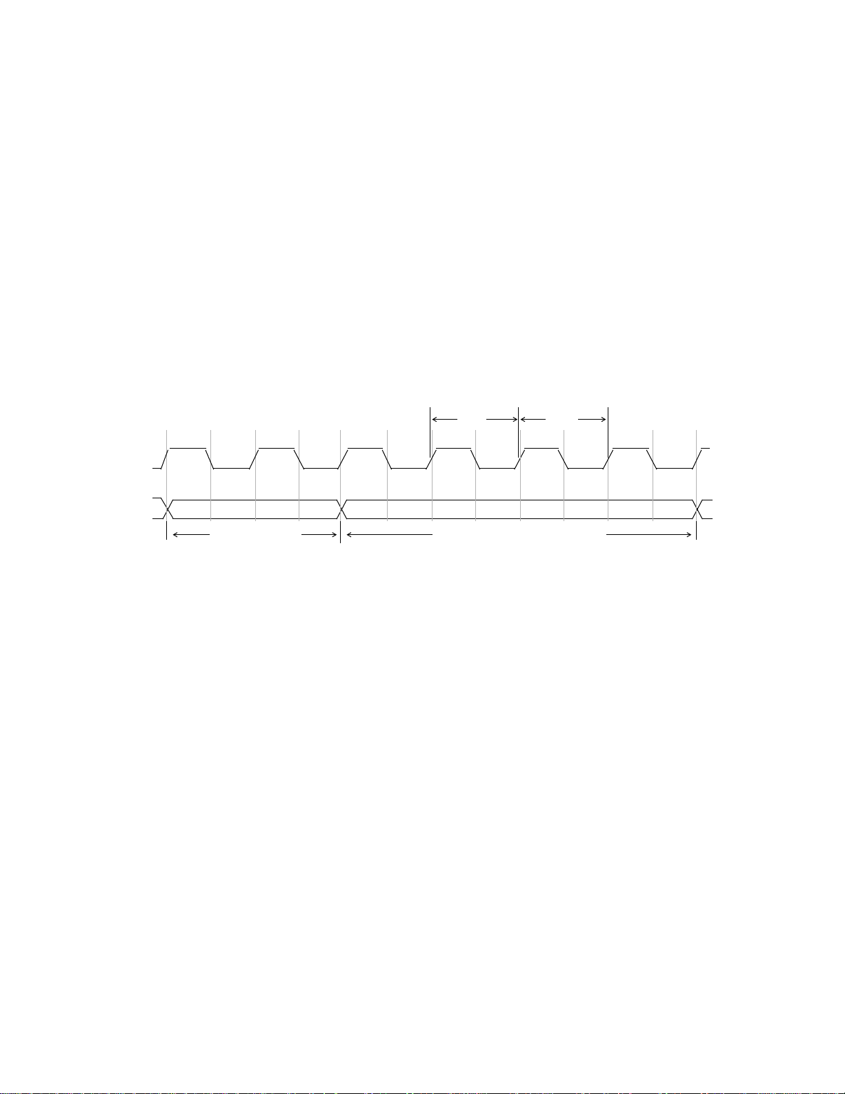
CLK (Clock Input) - active high input, high frequency processor clock. Frequency is twice the
instruction rate. An internal phase generator divides CLK into four phases (t0, t1, t2 and
t3) which is the basic instruction execution cycle. Additional tw phases are optionally
generated to insert wait states (WS) into instruction execution. A wait state is formed by
pairing a t2 and tw phase. CLK should be continuous with a 46-54% duty cycle.
WS WS
t0 t1 t2 t3 t0 t1 t2 tw t2 tw t2 t3
CLK
No Wait State
Instruction
Quiet VCC (4) (Power) - isolated power for the CPU logic. Must be tied to all other chip power pins ex-
ternally. User must provide adequate external decoupling capacitors.
Quiet VSS (4) (Ground) - isolated ground for the CPU logic. Must be tied to all other chip ground pins
externally. User must provide adequate external decoupling capacitors.
Address Bus VCC(4) (Power) - isolated power for sections of address bus I/O drivers. Must be tied to
all other chip power pins externally. User must provide adequate external decoupling
capacitors.
Address Bus VSS(8) (Ground) - isolated ground for sections of address bus I/O drivers. Must be tied
to all other chip ground pins externally. User must provide adequate external decoupling
capacitors.
Two Wait State Instruction
Data Bus VCC(4) (Power) - isolated power for sections of data bus I/O drivers. Must be tied to all
other chip power pins externally. User must provide adequate external decoupling capacitors.
Data Bus VSS(8) (Ground) - isolated ground for sections of data bus I/O drivers. Must be tied to
all other chip ground pins externally. User must provide adequate external decoupling
capacitors.
2 - 4 DSP96002 USER’S MANUAL MOTOROLA
Page 8

Bus Control VCC(2) (Power) - isolated power for the bus control I/O drivers. Must be tied to all other
chip power pins externally. User must provide adequate external decoupling capacitors.
Bus Control VSS(4) (Ground) - isolated ground for the bus control I/O drivers. Must be tied to all oth-
er chip ground pins externally. User must provide adequate external decoupling capacitors.
2.1.4 On-chip Emulator Interface (OnCE) (4 Pins)
—D–
R (Debug Request) - The debug enable input provides a means of entering the debug
mode of operation from the external command controller. This pin when asserted causes
the DSP96002 to finish the current instruction being executed, save the instruction pipeline information, enter the debug mode and wait for commands to be entered from the
debug serial input line.
DSCK/OS1 (Debug Serial Clock/Chip Status 1) - The DSCK/OS1 pin, when configured as an input,
is the pin through which the serial clock is supplied to the OnCE. The serial clock provides pulses required to shift data into and out of the OnCE serial port. When output (not
in Debug Mode), this pin in conjunction with the OS0 pin, provides information about the
chip status.
DSI/OS0 (Debug Serial Input/Chip Status 0) - The DSI/OS0 pin, when configured as an input, is
the pin through which serial data or commands are provided to the OnCE controller. The
data received on the DSI pin will be recognized only when the DSP 96002 has entered
the debug mode of operation. When configured as an output (not in Debug Mode), this
pin in conjunction with the OS1 pin, provides information about the chip status.
DSO (Debug Serial Output)
OnCE controller registers as specified by the last command received from the external
command controller. When a trace or breakpoint occurs this line will be asserted for one
T cycle to indicate that the chip has entered the debug mode and is waiting for commands.
The debug serial output provides the data contained in one of the
2.1.5 Port A and Port B (162 Pins)
Port A and Port B are identical in pinout and function. The following pin descriptions apply to both ports.
Each port may be a bus master and each port has a host interface which can be accessed on demand.
The pins are specified for a 50 pf load and two external TTL loads. Derating curves will be provided specifying performance up to 250 pf capacitive loads.
A0-A31 (Address Bus) - three-state, active high outputs when a bus master. When not a bus
master, A2-A5 are active high inputs, A0-A1 and A6-A31 are three-stated. As inputs,
A2-A5 may change asynchronous relative to the input clock (CLK). A2-A5 are host interface address inputs which are used to select the host interface register. When a bus
master, A0-A31 specify the address for external program and data memory accesses.
If there is no external bus activity, A0-A31 remain at their previous values. When a bus
master, the Address Enable (—A–E) input acts as an output enable control for A0-A31.
When a bus master, A0-A31 are stable whenever the transfer strobe —T–S is asserted
MOTOROLA DSP96002 USER’S MANUAL 2 - 5
Page 9

and may change only when —T–S is deasserted. A0-A31 are three-stated during hardware reset.
D0-D31 (Data Bus) - three-state, active high, bidirectional input/outputs when a bus master or
not a bus master. The Data Enable (—D–E) input acts as an output enable control for
D0-D31. As a bus master, the data lines are controlled by the CPU instruction execution
or the DMA controller. D0-D31 are also the Host Interface data lines. If there is no external bus activity, D0-D31 are three-stated. D0-D31 are also three-stated during hardware reset.
S1,S0 (Space Select) - three-state, active low outputs when a bus master, three-stated when
not a bus master. Timing is the same as the address lines A0-A31. S1 and S0 are threestated during hardware reset.
These signals can be viewed in different ways, depending on how the external memories are mapped. They support the trend toward splitting memory spaces among ports
and mapping multiple memory spaces into the same physical memory locations. Sev-
S1 S0 MEMORY SPACE
1 1 No access
1 0 P access
0 1 X access
0 0 Y access
eral examples are given in Figure 2-3 . The encoding S1:S0=11 may be used to place
external memories in their low power standby mode.
R/—W (Read/Write)- three-state, active low output when a bus master, active low input when
not a bus master. Bus master timing is the same as the DSP96002 address lines, giving
EXTERNAL MEMORY AND MAPPING S1 FUNCTION S0 FUNCTION
P only —
X only
Y only
X and Y mapped as 1 or 2 spaces
P and X mapped as 2 spaces
P and Y mapped as 1 space
P, X, and Y mapped as 1 space
—D–
—D–
—D–
—D–
—P–S/—D–S—P–
—P–S/—D–
S—
S—
SX/
S
S—
—P–
S
–
Y
—P–
S
S and —D–S
Figure 2-3. Program and Data Memory Select Encoding
2 - 6 DSP96002 USER’S MANUAL MOTOROLA
Page 10

an "early write" signal for DRAM interfacing. R/—W is high for a read access and is low
for a write access. The R/—W pin is also the Host Interface read/write input. As an input, R/—W may change asynchronous relative to the input clock. R/—W goes high if
the external bus is not used during an instruction cycle. R/—W is three-stated during
hardware reset.
—B–
S (Bus Strobe) - three-state, active low output when a bus master, three-stated when not
a bus master. Asserted at the start of a bus cycle (providing an "early bus start" signal
for DRAM interfacing) and deasserted at the end of the bus cycle. The early negation
provides an "early bus end" signal useful for external bus control. If the external bus is
not used during an instruction cycle, —B–S remains deasserted until the next external
bus cycle. —B–S is three-stated during hardware reset.
—T–
T (Transfer Type) - three-state, active low output when a bus master, three-stated when
not a bus master. When a bus master, —T–T is controlled by an on-chip page circuit
(see Section seven). —T–T is asserted when a fast access memory mode (page, static
column, nibble or serial shift register) is detected. If the external bus is not used during
an instruction cycle or a fault is detected by the page circuit during an external access,
—T–
T remains deasserted. The parameters of the page circuit fault detection are user
programmable. —T–T is three-stated during hardware reset.
—T–
S (Transfer Strobe) - three-state, active low output when a bus master, active low input
when not a bus master. When a bus master, —T–S is asserted to indicate that the address lines A0-A31, S1, S0, —B–S, —B–L and R/—W are stable and that a bus read or
bus write transfer is taking place. During a read cycle, input data is latched inside the
DSP96002 on the rising edge of —T–S. During a write cycle, output data is placed on
the data bus after —T–S is asserted. Therefore —T–S can be used as an output enable
control for external data bus buffers if they are present. If the external bus is not used
during an instruction cycle, —T–S remains deasserted until the next external bus cycle.
An external flip-flop can delay —T–S if required for slow devices or more address decoding time. The —T–S pin is also the Host Interface transfer strobe input used to en-
able the data bus output drivers during host read operations and to latch data inside the
Host Interface during host write operations. As an input, —T–S may change asynchro-
nous relative to the input clock. Write data is latched inside the Host Interface on the
rising edge of —T–S. —T–S is three-stated during hardware reset.
MOTOROLA DSP96002 USER’S MANUAL 2 - 7
Page 11
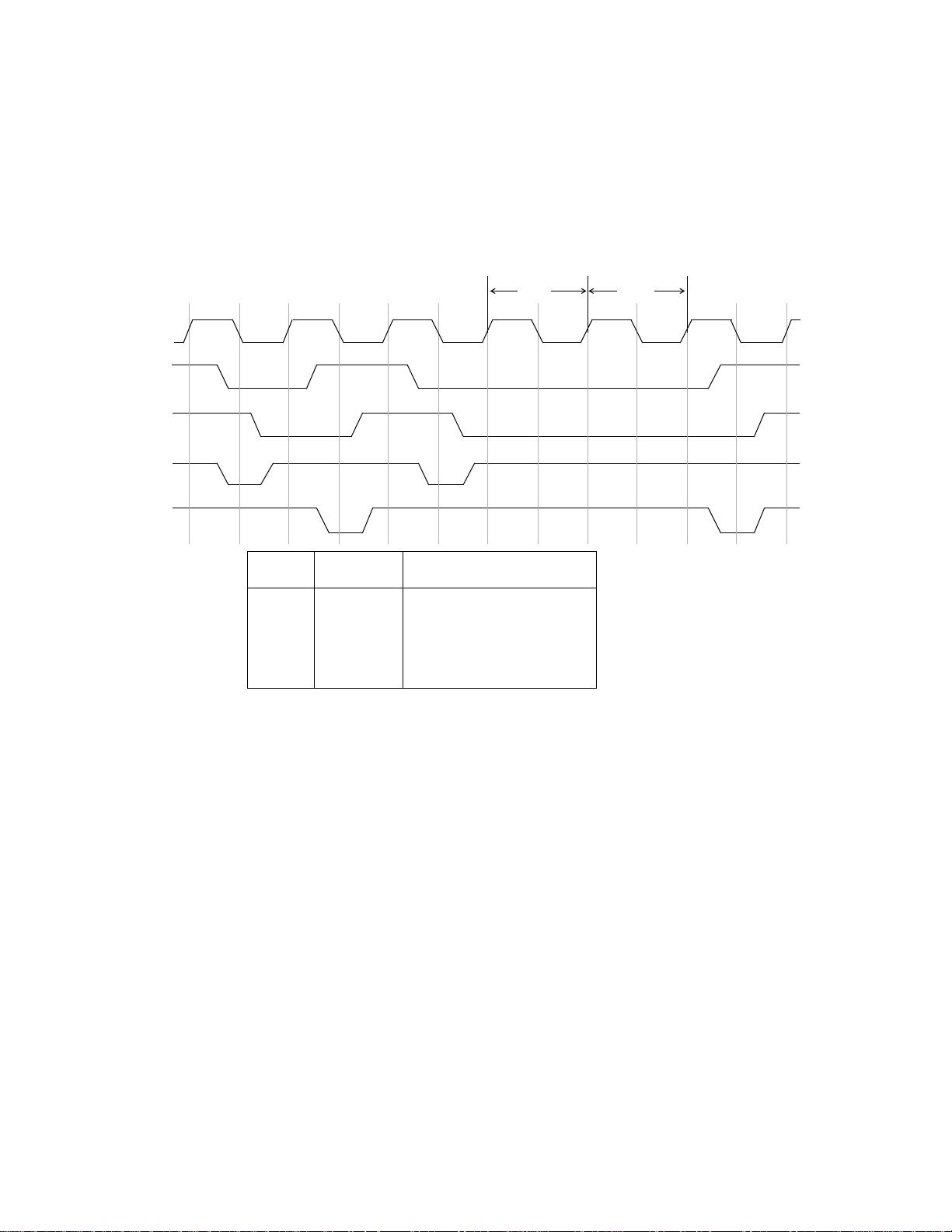
CLK
—B–
—T–
When a bus master, the combination of —B–S and —T–S can be decoded externally to
determine the status of the current bus cycle and to generate hardware strobes useful
for latching address and data signals. The encoding is shown in Figure 2-4.
WS WS
t0 t1 t2 t3 t0 t1 t2 tw t2 tw t2 t3
S
—A–
—D–
—B–S—T–
1 1 Idle
0 1 Cycle Start Address Strobe (—A–S)
0 0 Wait
1 0 Cycle End Data Strobe (—D–S)
S Bus Status Strobe Generation Application
Figure 2-4. Bus Status Encoding
—T–
A (Transfer Acknowledge) - active low input. If the DSP96002 is the bus master and either
there is no external bus activity or the DSP96002 is not the bus master, the —T––A input
is ignored by the core. The —T–A input is a synchronous "DTACK" function which can
extend an external bus cycle indefinitely. —T–A must be asserted and deasserted synchronous to the input clock (CLK) for proper operation. —T–A is sampled on the falling
edge of the input clock (CLK). Any number of wait states (0, 1, 2, ..., infinity) may be
inserted by keeping —T–A deasserted. In typical operation, —T–A is deasserted at the
start of a bus cycle, is asserted to enable completion of the bus cycle and is deasserted
before the next bus cycle. The current bus cycle completes one clock period after —T
A is asserted synchronous to CLK. The number of wait states is determined by the
T–A input or by the Bus Control Register (BCR), whichever is longer. The BCR can be
used to set the minimum number of wait states in external bus cycles. If —T–A is tied
low (asserted) and no wait states are specified in the BCR register, zero wait states will
be inserted into external bus cycles.
2 - 8 DSP96002 USER’S MANUAL MOTOROLA
–
—
Page 12

—A–
E (Address Enable) - active low input, must be asserted and deasserted synchronous to
the input clock (CLK) for proper operation. If a bus master, —A–E is asserted to enable
the A0-A31 address output drivers. If —A–E is deasserted, the address output drivers
are three-stated. If not a bus master, the address output drivers are three-stated regardless of whether —A–E is asserted or deasserted. The function of —A–E is to allow mul-
tiplexed bus systems to be implemented. Examples are a multiplexed address/data bus
such as the NuBus used in the Macintosh II or a multiplexed address1/address2 bus
used with dual port memories such as dynamic VRAMs. Note that there must be at least
one undriven CLK period between enables for multiplexed buses to allow one bus to
three-state before another bus is enabled. External control is responsible for this timing.
For non-multiplexed systems, —A–E should be tied low.
—D–
E (Data Enable) - active low input, must be asserted and deasserted synchronous to the
input clock (CLK) for proper operation. If a bus master or the Host interface is being read,
—D–
E is asserted to enable the D0-D31 data bus output drivers. If —D–E is deassert-
ed, the data bus output drivers are three-stated. If not a bus master, the data bus output
drivers are three-stated regardless of whether —D–E is asserted or deasserted. Readonly bus cycles may be performed even though —D–E is deasserted. The function of
—D–
E is to allow multiplexed bus systems to be implemented. Examples are a multi-
plexed address/data bus such as the NuBus used in the Macintosh II or a multiplexed data1/data2 bus used for long word transfers with one 32 bit wide memory. Note
that there must be at least one undriven CLK period between enables for multiplexed
buses to allow one bus to three-state before another bus is enabled. External control is
responsible for this timing. For non-multiplexed systems, —D–E should be tied low.
—H–
S (Host Select) - active low input, may change asynchronous to the input clock. —H–S is
asserted low to enable selection of the Host Interface functions by the address lines A2A5. If —T–S is asserted when —H–S is asserted, a data transfer will take place with the
Host Interface. Note that both —H–S and —H–A must be tied high to disable the Host
Interface. When —H–A is asserted, —H–S is ignored.
—H–
A (Host Acknowledge) - active low input, may change asynchronous to the input clock.
H–A is used to acknowledge either an interrupt request or a DMA request to the host
—
interface. When the host interface is not in DMA mode, asserting —T–S when —H–A
and —H–R are asserted will enable the contents of the host interface interrupt vector
NuBus is a trademark of Texas Instruments, Inc.
Macintosh II is a trademark of Apple Computer, Inc.
MOTOROLA DSP96002 USER’S MANUAL 2 - 9
Page 13

register (IVR) onto the data bus outputs D0-D31. This provides an interrupt acknowledge capability compatible with MC68000 family processors.
If the host interface is in DMA mode, —H–A is used as a DMA transfer acknowledge input and it is asserted by an external device to transfer data between the Host Interface
registers and an external device. In DMA read mode, —H–A is asserted to read the Host
Interface RX register on the data bus outputs D0-D31. In DMA write mode, —H–A is as-
serted to strobe external data into the Host Interface TX register. Write data is latched
into the TX register on the rising edge of —H–A.
—H–
R (Host Request) - active low output, never three-stated. The host request —H–R is as-
serted to indicate that the host interface is requesting service - either an interrupt request
or a DMA request - from an external device.
The —H–R output may be connected to interrupt request input —I—R—Q–A, —I—R
Q–B, or —I—R—Q–C of another DSP96002. The DSP96002 on-chip DMA Controller
channel can select the interrupt request input as a DMA transfer request input.
—B–
R (Bus Request) - active low output, never three-stated. —B–R is asserted when the CPU
or DMA is requesting bus mastership. —B–R is deasserted when the CPU or DMA no
longer needs the bus. —B–R may be asserted or deasserted independent of whether
the DSP96002 is a bus master or a bus slave. Bus "parking" allows —B–R to be
deasserted even though the DSP96002 is the bus master. See the description of bus
"parking" in the —B–A pin description. The RH bit in the Bus Control Register (see
Section seven) allows —B–R to be asserted under software control even though the
CPU or DMA does not need the bus. —B–R is typically sent to an external bus arbitrator
which controls the priority, parking and tenure of each DSP96002 on the same external
bus. —B–R is only affected by CPU or DMA requests for the external bus, never for the
internal bus. During hardware reset, —B–R is deasserted and the arbitration is reset
to the bus slave state.
—
—B–
G (Bus Grant) – active low input. —B–G must be asserted/ deasserted synchronous to the
input clock (CLK) for proper operation. —B–G is asserted by an external bus arbitration
circuit when the DSP96002 may become the next bus master. When —B–G is asserted,
the DSP96002 must wait until —B–B is deasserted before taking bus mastership. When
—B–
G is deasserted, bus mastership is typically given up at the end of the current bus
cycle. This may occur in the middle of an instruction which requires more than one external bus cycle for execution. Note that indivisible read-modify-write instructions
2 - 10 DSP96002 USER’S MANUAL MOTOROLA
Page 14

(BSET, BCLR, BCHG) will not give up bus mastership until the end of the current instruc-
——B–
tion.
—B–
A (Bus Acknowledge) - Open drain, active low output. When deasserting —B–A, the
DSP96002 drives —B–A high during half a CLK cycle and then disables the active pullup. In this way, only a weak external pull-up resistor is required to hold the line high.
G is ignored during hardware reset.
—
B–A may be directly connected to —B–B
MC68040 —B–B pin. When —B–G is asserted, the DSP96002 becomes the pending
bus master. It waits until —B–B is negated by the previous bus master, indicating that
the previous bus master is off the bus. The pending bus master asserts —B–A to become the current bus master. —B–A is asserted when the CPU or DMA has taken the
bus and is the bus master. While —B–A is asserted, the DSP96002 is the owner of the
bus (the bus master). When —B–A is negated, the DSP96002 is a bus slave. —B–A
may be used as a three-state enable control for external address, data and bus control
signal buffers. —B–A is three-stated during hardware reset.
Note that a current bus master may keep —B–A asserted after ceasing bus activity, regardless of whether —B–R is asserted or deasserted. This is called "bus parking" and
allows the current bus master to use the bus repeatedly without re-arbitration until some
other device wants the bus.
The current bus master keeps —B–A asserted during indivisible read-modify-write bus
cycles, regardless of whether —B–G has been deasserted by the external bus arbitra-
tion unit. This form of "bus locking" allows the current bus master to perform atomic operations on shared variables in multitasking and multiprocessor systems. Current instructions which perform indivisible read-modify-write bus cycles are BCLR, BCHG and
BSET.
in order to obtain the same functionality as the
—B–
B (Bus Busy) - active low input, must be asserted and deasserted synchronous to the input
clock (CLK) for proper operation. —B–B is deasserted when there is no bus master on
the external bus. In multiple DSP96002 systems, all —B–B inputs are tied together and
are driven by the logical AND of all —B–A outputs. —B–B is asserted by a pending bus
master (directly or indirectly by —B–A assertion) to indicate that it is now the current bus
master. —B–B is deasserted by the current bus master (directly or indirectly by —B–A
negation) to indicate that it is off the bus and is no longer the bus master. The pending
bus master monitors the —B–B signal until it is deasserted. Then the pending bus master asserts —B–A to become the current bus master, which asserts —B–B directly or
indirectly.
MOTOROLA DSP96002 USER’S MANUAL 2 - 11
Page 15

—B–
L (Bus Lock) - active low output, never three-stated. Asserted at the start of an external
indivisible Read-Modify-Write (RMW) bus cycle (providing an "early bus start" signal for
DRAM interfacing) and deasserted at the end of the write bus cycle. —B–L remains asserted between the read and write bus cycles of the RMW bus sequence. —B–L can
be used to indicate that special memory timing (such as RMW timing for DRAMs) may
be used or to "resource lock" an external multi-port memory for secure semaphore updates. The early negation provides an "early bus end" signal useful for external bus con-
trol. If the external bus is not used during an instruction cycle, —B–L remains deasserted until the next external indivisible RMW bus cycle. —B–L also remains deasserted if
the external bus cycle is not an indivisible RMW bus cycle or if there is an internal RMW
bus cycle. The only instructions which automatically assert —B–L are a BSET, BCLR
or BCHG instruction which accesses external memory. —B–L can also be asserted by
setting the LH bit in the BCR register (see Section seven). —B–L is deasserted during
hardware reset.
2.1.6 Reserved Pins
There are 5 spare pins reserved for future use.
2.2 BUS OPERATION
The external bus timing is defined by the operation of the Address Bus, Data Bus and Bus Control pins
described in paragraph 2.1.5. The DSP96002 external ports are designed to interface with a wide variety
of memory and peripheral devices, high speed static RAMs, dynamic RAMs and video RAMs as well as
slower memory devices. External bus timing is controlled by the —T–A control signal and by the Bus Control Registers (BCR) which are described in Section seven. The BCR and —T–A control the timing of the
bus interface signals. Insertion of wait states is controlled by the BCR to provide constant bus access timing, and by —T–A to provide dynamic bus access timing. The number of wait states is determined by the
—T–
A input or by the BCR, whichever is longer.
2.2.1 Synchronous Bus Operation
Synchronous external bus cycle consists of at least 4 internal clock phases. See the DSP96002 Technical
Data Sheet (DSP96002/D) for the specification of the internal clock phases. Each synchronous external
memory access requires the following procedure:
3:3. The external memory address is defined by the Address Bus A0-A31 and the Memory Ref-
erence Select signals S1 and S0. These signals change in the first phase of the external bus
cycle. The Memory Reference Select signals have the same timing as the Address Bus and
may be used as additional address lines. The Address and Memory Reference signals are
also used to generate chip select signals for the appropriate memory chips. These chip select signals change the memory chips from low power standby mode to active mode and begin the read access time. This allows slower memories to be used since the chip select signals are address-based rather than read or write enable-based.
2 - 12 DSP96002 USER’S MANUAL MOTOROLA
Page 16

3:4. When the Address and Memory Reference signals are stable, the data transfer is enabled by
the Transfer Strobe —T–S signal. —T–S is asserted to "qualify" the Address and Memory
Reference signals as stable and to perform the read or write data transfer. —T–S is asserted
in the second phase of the bus cycle.
3:5. Wait states are inserted into the bus cycle controlled by a wait state counter or by —T–A,
whichever is longer. The wait state counter is loaded from the Bus Control Register. If the
wait state number determined by these two factors is zero, no wait states are inserted into
the bus cycle and —T–S is deasserted in the fourth phase. If the wait state number determined is W, then W wait states are inserted into the instruction cycle. Each wait state introduces one Tc delay.
3:6. When the Transfer Strobe —T–S is deasserted at the end of a bus cycle, the data is latched
in the destination device. At the end of a read cycle, the DSP96002 latches the data internally. At the end of a write cycle, the external memory latches the data. The Address signals
remain stable until the first phase of the next external bus cycle to minimize power dissipation. The Memory Reference signals S1 and S0 are deasserted during periods of no bus activity and the data signals are three-stated.
3.6.1 Static RAM Support
Static RAM devices can be easily interfaced to the DSP96002 bus timing. There are two basic techniques
- —C–S controlled writes and —W–E controlled writes.
—C–
3. 6.1.1
This form of static interface uses the memory chip select (—C–S) as the write strobe. The DSP96002 R/
—
W signal is used as an early read/write direction indication. Proper data buffer enable control on RAMs
without a separate output enable (—O–E) input must use this form to avoid multiple data buffers colliding
on the data bus. The interface schematic is shown in Figure 2-5.
DSP96002
S Controlled Writes
—T–
—C–
—W–
S
ER/—W
STATIC RAM
Figure 2-5. —C–S Controlled Writes Interface to Static RAM
MOTOROLA DSP96002 USER’S MANUAL 2 - 13
Page 17
The disadvantage of this technique is that access time is measured from —T–S instead of from the address
or —B–S. Hence faster memories are required.
DSP96002
S1 or S0
R/
—
—
STATIC RAM
—
—O–
—C–
Figure 2-6. —W–E Controlled Writes Interface To Static RAM
—W–
3. 6.1.2
This form of static interface uses the memory write enable (—W–E) as the write strobe. The DSP96002
R/—W signal is used to form a late read/write indication by gating it with —T–S. This form is the one used
by the 56000/1 bus interface. Proper data buffer enable control requires a separate output enable (—O
E) input on the memory to avoid multiple data buffers colliding on the data bus. The interface schematic
is shown in Figure 2-6.
E Controlled Writes
–
The advantage of this technique is that access time is measured from S1, S0 or addresses instead of
T–S. Hence slower memories can be used. The disadvantage of this technique is that the write data hold
will be shortened because the —W–E signal is delayed by the OR gate.
3.6.2 Dynamic RAM and Video RAM Support
Modern dynamic memory (DRAM) and video memory (VRAM) are becoming the preferred choice for a
wide variety of computing systems based on
4:7. Cost per bit due to dynamic storage cell density.
4:8. Packaging density due to multiplexed address and control pins.
4:9. Improved performance relative to static RAMs due to fast access modes (page, static col-
umn, nibble and serial shift (VRAM)).
4:10. Commodity pricing due to high volume production.
2 - 14 DSP96002 USER’S MANUAL MOTOROLA
—
Page 18

The Port A/B bus control signals are designed for efficient interface to DRAM/VRAM devices in both random read/write cycles and fast access modes such as those listed above. The bus control signal timing
is specified relative to the external clock (CLK) to enable synchronous control by an external state ma-
chine. An on-chip page circuit controls the —T–T pin, indicating to the external state machine when a slow
or fast access is being made. The page circuit operation and programming is described in Section seven.
4.11 BUS HANDSHAKE AND ARBITRATION
Bus transactions are governed by a single bus master. Bus arbitration determines which device becomes
the bus master. The arbitration logic implementation is system dependent, but must result in at most one
device becoming the bus master (even if multiple devices request bus ownership). The arbitration signals
permit simple implementation of a variety of bus arbitration schemes (e.g. fairness, priority, etc.). External
logic must be provided by the system designer to implement the arbitration scheme.
4.11.1Bus Arbitration Signals
Four signals are provided for bus arbitration. Three of them are considered as local arbitration signals and
one as system arbitration signal. The local arbitration signals run between a potential bus master and the
arbitration logic. The local signals are —B–R, —B–G, and —B–A; —B–B is a system arbitration signal.
These signals are described below.
—B–
R Bus Request - Asserted by the requesting device to indicate that it wants to use the bus,
and is held asserted until it no longer needs the bus. This includes time when it is the
bus master as well as when it is not the bus master.
—B–
G Bus Grant - Asserted by the bus arbitration controller to signal the requesting device that
it is the bus master elect. —B–G is valid only when the bus is not busy (Bus Busy signal
described below).
—B–
A Bus Acknowledge - Asserted by the device (bus master) that received the bus owner-
ship from the bus arbitration controller. The master holds —B–A asserted for the duration of its bus possession. —B–A indicates whether the device is a bus master or a bus
slave. When asserted, —B–A indicates that the device is the bus master. —B–A may
be used as a three-state enable control for external address, data and bus control signal
buffers.
—B–
B Bus Busy - The system arbitration signal —B–B is monitored by all potential bus masters
and is derived from the local bus signal —B–A. This signal controls the hand-over of
bus ownership by the bus master at the end of bus possession. Typically —B–B is the
wired-OR of all bus acknowledgments. —B–B is asserted if the Bus Acknowledge signal
is asserted by the bus master.
MOTOROLA DSP96002 USER’S MANUAL 2 - 15
Page 19

4.11.2The Arbitration Protocol
The bus is arbitrated by a central bus arbitrator, using individual request/grant lines to each bus master.
The arbitration protocol can operate in parallel with bus transfer activity so that the bus hand-over can be
made without much performance penalty.
The arbitration sequence occurs as follows:
5:12. All candidates for bus ownership assert their respective —B–R signals as soon as they need
the bus.
5:13. The arbitration logic designates a bus master-elect by asserting the —B–G signal for that de-
vice.
5:14. The master-elect tests —B–B to ensure that the previous master has relinquished the bus.
If —B–B is deasserted, then the master-elect asserts —B–A, which designates the device as
the new bus master. If a higher priority bus request occurs before the —B–B signal was
deasserted, then the arbitration logic may replace the current master-elect with the higher
priority candidate. However, only one —B–G signal must be asserted at one time.
5:15. The new bus master begins its bus transfers after the assertion of —B–A.
5:16. The arbitration logic signals the current bus master to relinquish the bus by deasserting —B
G at any time. A DSP96002 bus master releases its ownership (deasserts —B–A) after
completing the current external bus access. If an instruction is executing a Read-Modify-
Write external access, a DSP96002 master asserts the —B–L signal and will only relinquish
the bus (and deassert —B–L) after completing the entire Read-Modify-Write sequence.
When the current bus master deasserts —B–A, the —B–B signal must also be deasserted
because the next bus master-elect has received its —B–G signal and is waiting for —B–B to
be deasserted before claiming ownership.
The DSP96002 has 2 control bits and one status bit, located in the Bus Control Registers (see Section 7)
to permit software control of the —B–R and —B–L signals, and to verify when the chip is the bus master.
If the RH bit in the BCR register is cleared, the DSP96002 asserts its —B–R signal only as long as requests
for bus transfers are pending or being attempted. If the RH bit is set, —B–R will remain asserted. If the
LH bit in the BCR register is cleared, the DSP96002 asserts its —B–L signal only during a read-modify-
–
write bus access. If the LH bit is set, —B–L will remain asserted.
5.16.1Arbitration Scheme
The bus arbitration scheme is implementation dependent. The diagram in Figure 2-7 illustrates a common
method of implementing the bus arbitration scheme. The arbitration logic determines the device priorities
and assigns bus ownership depending on those priorities.
2 - 16 DSP96002 USER’S MANUAL MOTOROLA
Page 20
An implementation of a bus arbitration scheme may hold —B–G asserted, for example, to the current bus
owner if none of the other devices are requesting the bus. As a consequence, the current bus master may
keep —B–A asserted after ceasing bus activity, regardless of whether —B–R is asserted or deasserted.
This situation is called "bus parking" and allows the current bus master to use the bus repeatedly without
re-arbitration until some other device requests the bus.
V
cc
DSP96002
DSP96002
—B–
—B–
—B–
—B–
—B–
ARBITRATION
LOGIC
L
—B–
—B–
—B–
—B–
—B–
L
Figure 2-7. Bus Arbitration Scheme
5.16.2Bus Handshake Unit
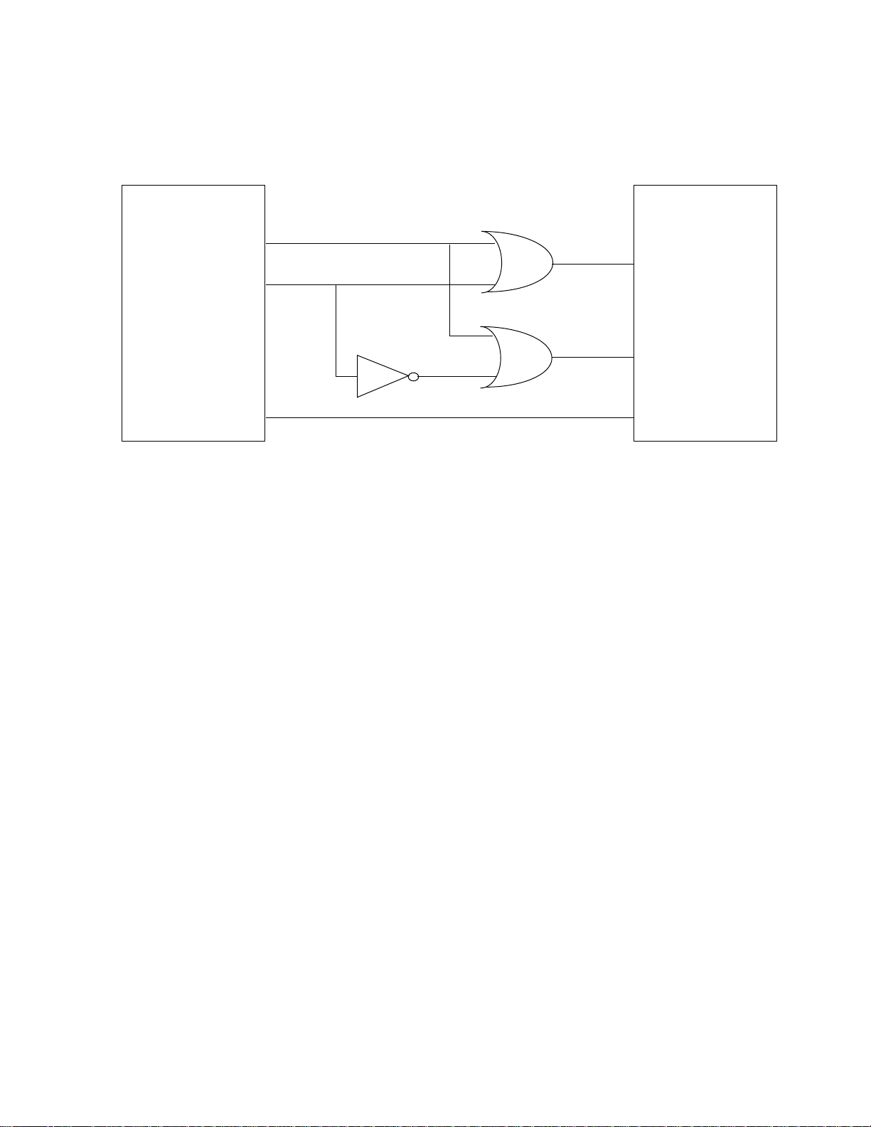
The bus handshake unit in the DSP96002 is implemented within a finite state machine. It consists of two
external outputs (—B–R, —B–A), two external inputs (—B–G, —B–B) and three internal inputs
(ext_acc_req, end_of_sequence, RH) (see Figure 2-8). The ext_acc_req signal is asserted when one or
more requests for external bus access are pending, and remains asserted as long as the transfers are
being executed. The end_of_sequence signal is asserted at the last bus cycle of the current sequence.
—B–
ext_acc_req
end_of_sequence
Request Hold (RH)
BUS
HANDSHAKE
UNIT
—B–
—B–
—B–
B
R
A
Figure 2-8. Bus Handshake Unit
MOTOROLA DSP96002 USER’S MANUAL 2 - 17
Page 21

YY
(delayed
ZZ
(delayed)
REQUEST_BUS
(Y)
—B–R = 0
—B–A = 1
ZY
)
ACTIVE_
MASTER
(Z)
—B–R = 0
—B–A = 0
YZ
WY
(non-existant)
XZ
YX (illegal)
XY
ZW
WZ
ZX
YW (illegal)
IDLE
(X)
—B–R = —R
H
WX
PARKING_
MASTER
(W)
—B–R =
R–H
XW
XX
–
—
WW
Figure 2-9. Bus Handshake State Diagram
Likewise, when executing the read part of a RMW access, the end_of_sequence signal is deasserted.
This signal is used to give up bus ownership if —B–G is deasserted during bus transfers. The state ma-
chine which controls the bus handshake is illustrated in Figure 2.9.
The transition arcs are labeled by two letters which denote its source and destination states. The equa-
tions of the transition arcs are described as follows:
XX = ^ext_acc_req & ^( ^—B–G & —B–B )
XY = ext_acc_req & ^( ^—B–G & —B–B )
XZ = ext_acc_req & ( ^—B–G & —B–B )
XW = ^ext_acc_req & ( ^—B–G & —B–B )
YX = ^ext_acc_req & ^( ^—B–G & —B–B ) (note 1)
YY = ext_acc_req & ^( ^—B–G & —B–B )
YZ = ext_acc_req & ( ^—B–G & —B–B )
YW = ^ext_acc_req & ( ^—B–G & —B–B ) (note 1)
ZX = ^ext_acc_req & —B–G
ZY = ext_acc_req & —D—B–G & end_of_sequence (note 3)
2 - 18 DSP96002 USER’S MANUAL MOTOROLA
Page 22

ZZ = ^end_of_sequence v ( ext_acc_req & ^—D—B–G ) (note 3)
ZW = ^ext_acc_req & ^—B–G
WX = ^ext_acc_req & —B–G
WY = NON-EXISTENT ARC (note 2)
WZ = ext_acc_req
WW = ^ext_acc_req & ^—B–G
Notes: 1. Illegal arcs in DSP96002 since once the request of the bus is pending, it will not be canceled
before the execution of the access.
2. Non-existent arc since if ext_acc_req arrives together with the negation of —B–G, the device
becomes active master and begins its bus transfers.
3.—D—B–G is —B–G delayed by one phase. This is done to provide a response to the
ext_acc_req signal when it is asserted at the same phase together with —B–G negation.
5.16.3Bus Arbitration Example Cases
5.16.3.1 Case 1 – Normal
If the device requesting mastership asserts —B–R: the arbiter asserts the requesting devices’ —B–G and
—B–
B is deasserted indicating the bus is not busy. The requesting device will assert —B–A.
5.16.3.2 Case 2 – Bus Busy
If the device requesting mastership asserts —B–R: the arbiter responds by asserting the requesting devices’ —B–G; however, the bus is busy because —B–B is asserted. The requesting device will not assert
B–A until —B–B is deasserted.
5.16.3.3 Case 3 – Low Priority
If the device requesting mastership asserts —B–R: the arbiter withholds asserting the requesting devices’
—B–
G because a higher priority device requested the bus. —B–A of the requesting device will not be as-
serted.
—
5.16.3.4 Case 4 – Default
If a device does not request the bus and it is not in the bus parking state but rather it is in the idle state: the
arbiter, by design (i. e., default), asserts —B–G. —B–A will remain deasserted.
MOTOROLA DSP96002 USER’S MANUAL 2 - 19
Page 23
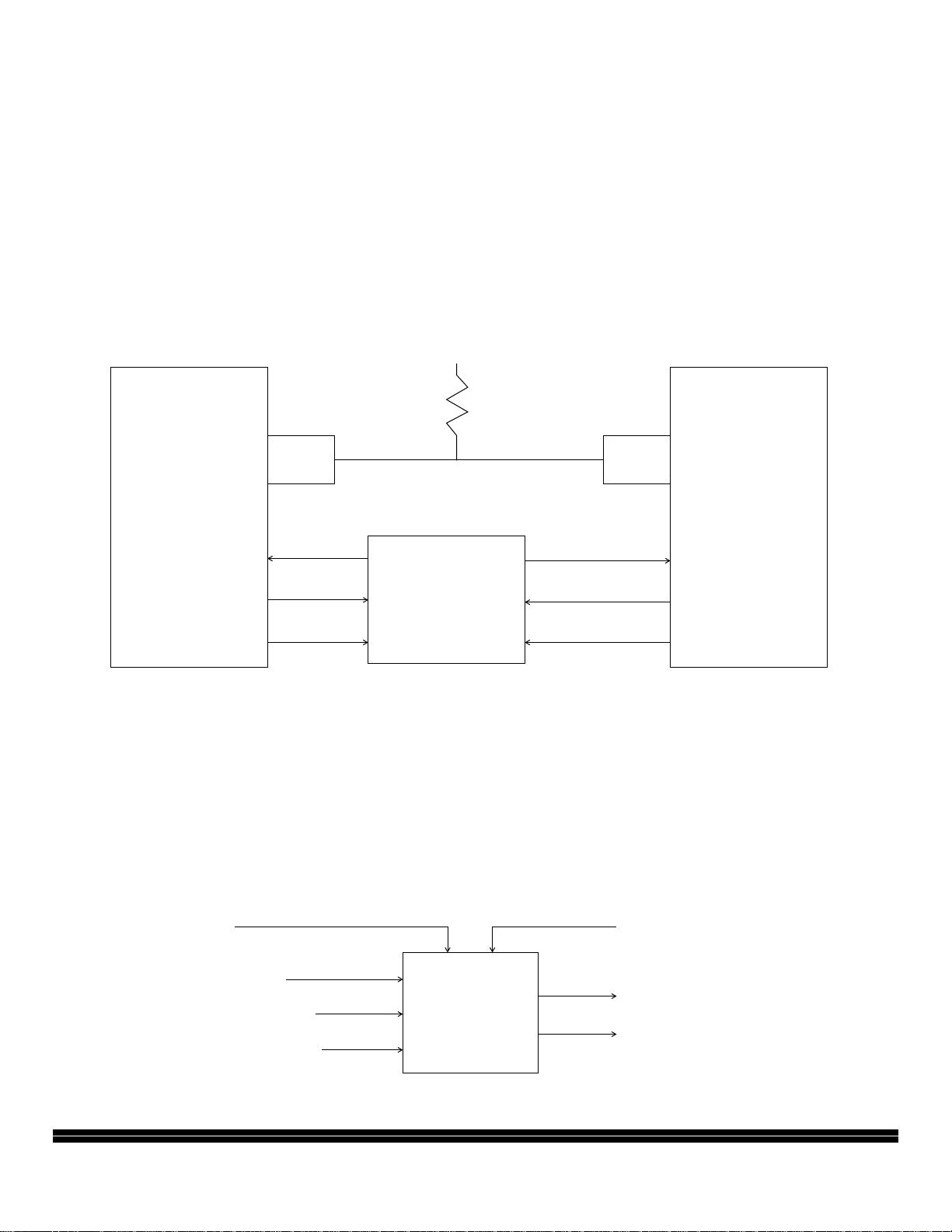
5.16.3.5 Case 5 – Bus Lock during RMW
If the device requesting mastership asserts —B–R and the arbiter asserts the requesting devices’ —B–G
and —B–B is deasserted, then the requesting device will assert —B–A. If a read-modify-write (RMW) instruction which accesses external memory is being executed, and the bus arbiter deasserts —B–G, then
—B–
A will remain asserted until the entire RMW instruction completes execution. —B–A will then be deasserted thereby relinquishing the bus. Note that during external RMW instruction execution, —B–L is asserted. In general, the —B–L signal can be used to ensure that a multiport memory can only be written by one
master at a time. That is, referring to Figure 2-10, —B–L can be input from DSP #1to the memory controller
which prevents —T–A from being asserted by the controller (thereby suspending the memory access by
DSP #2) until DSP #1 completes its RMW access.
DSP96002
RMW
—B–
Dual Port
Memory
Controller
L
—T–
A
DSP96002
#2#1
Figure 2-10. Bus Lock During RMW
5.16.3.6 Case 6 – Bus Park
The device requesting mastership asserts —B–R; the arbiter asserts the requesting devices’ —B–G and
—B–
B is deasserted indicating the bus is not busy – the requesting device will assert —B–A. When the
requesting device no longer requires the bus it will deassert —B–R; if the bus arbiter leaves —B–G asserted because other requests are not pending, then —B–A will remain asserted. This condition is called bus
parking and eliminates the need for the last bus master to rearbitrate for the bus during its next external
access.
2 - 20 DSP96002 USER’S MANUAL MOTOROLA
Page 24

SECTION 3
CHIP ARCHITECTURE
3.1 INTRODUCTION
The DSP96002 architecture is a 32-bit highly-parallel multiple-bus IEEE floating-point processor. The architecture is designed to accommodate various IC family members with different memory and on-chip peripheral requirements while maintaining a standard programmable core. The overall chip architecture is
presented and detailed block diagrams of the Data ALU and Address Generation Unit AGU) core architecture are described.
3.2 DSP96002 BLOCK DIAGRAM
The major components of the DSP96002 are
• Data Buses
• Address Buses
• Data ALU
• Address Generation Unit
• X Data Memory
• Y Data Memory
• Program Control and System Stack
• Program Memory
• Port A and Port B External Bus Interfaces
• Internal Bus Switch and Bit Manipulation Unit
• I/O Interfaces
An overall block diagram of the DSP96002 architecture is shown in Figure 3-1.
3.2.1 Data Buses
Data movement on the chip occurs over five bidirectional 32-bit buses, X Data Bus (XDB), Y Data Bus
(YDB), Global Data Bus (GDB), the DMA Data Bus (DDB) and the Program Data Bus (PDB). The X and Y
data buses may also be treated by certain instructions as one 64-bit data bus by concatenation of XDB and
YDB. Data transfer between the Data ALU and the X Data Memory and Y Data Memory occur over the X
Data Bus and Y Data Bus. These are kept local on the chip to maximize speed and minimize power. The
direct memory access data transfers occur over the DMA Data Bus. Program memory data transfers and
instruction fetches occur over the Program Data Bus. All other data transfers occur over the Global Data
Bus.
MOTOROLA DSP96002 USER’S MANUAL 3 - 1
Page 25

Figure 3-1. DSP96002 Block Diagram
3.2.2 Address Buses
Addresses are specified for internal X Data Memory and Y Data Memory on two unidirectional 32-bit buses,
X Address Bus (XAB) and Y Address Bus (YAB). Internal address bus sizes depend on the amount of internal memory implemented. External memory spaces for each port, A and B, are addressed via a single
32-bit unidirectional address bus driven by a three input multiplexer that can select the X Address Bus
(XAB), the Y Address Bus (YAB) or the Program Address Bus (PAB). On-chip peripherals and the DMA
Controller are memory mapped in the internal X memory space. When zero wait state external memory is
used, one instruction cycle is needed for each external memory access.
The XAB, YAB and PAB are dual access buses in the sense that one instruction cycle contains two slots,
the one slot is dedicated to the on-chip DMA transfers and the second is used for the core transfers.
3 - 2 DSP96002 USER’S MANUAL MOTOROLA
Page 26

3.2.3 Data ALU
The Data ALU performs all of the arithmetic and logical operations on data operands. The Data ALU consists of ten 96-bit general purpose registers, a 32-bit barrel shifter, a 32-bit adder, and a 32-bit parallel multiplier. Data ALU registers may be read or written over the XDB and YDB as 32 or 64-bit operands. The
Data ALU is capable of multiplication, addition, subtraction, format conversion, shifting and logical operations in one instruction cycle. Data ALU source operands may be 32 or 96-bits and originate from the general purpose register file. Data ALU results are always stored in one of the general purpose registers. Floating-point Data ALU operations always have a 96-bit result. Integer (fixed-point) Data ALU operations have
a 32 or 64-bit result.
The Data ALU fully implements the IEEE Standard 754 for binary floating-point arithmetic. The operations
are supported in three data formats: 32-bit two’s-complement fixed-point, 32-bit unsigned-magnitude fixedpoint and 44-bit IEEE single extended precision floating-point. All the floating-point computations are performed using the single extended precision format and the results are automatically rounded to single precision or single extended precision numbers as programmed. All four IEEE rounding modes (round to zero,
round to nearest, round to plus infinity and round to minus infinity) are supported for all floating-point operations and conversions. The IEEE gradual underflow with denormalized numbers is supported by the IEEE
mode. In the IEEE mode, if input operand(s) or output result(s) are denormalized numbers, additional instruction cycles are required to process these numbers per the IEEE standard. A "Flush to Zero" mode is
also provided which forces all floating point result underflows to zero (all denormalized input operands are
considered as being zero). The Flush to Zero mode never requires any additional instruction cycles.
Refer to Section 3.3 for a detailed description of the Data ALU architecture.
3.2.4 AGU
The AGU performs all of the address storage and effective address calculations necessary to address data
operands in memory and it is used by both the core and the on-chip DMA Controller. The AGU operates in
parallel with other chip resources to minimize address generation overhead. The AGU contains eight Address Registers (R0-R7), eight Offset Registers (N0-N7), and eight Modifier Registers (M0-M7). The Address Registers are 32-bit registers which may contain any address or data. Each Address Register may
be accessed for output to the XAB, YAB, and PAB. The modifier and offset registers are 32-bit registers
which are normally used to control updating of the address registers.
AGU registers may be read or written over the Global Data Bus as 32-bit operands. The AGU can generate
two 32-bit addresses every instruction cycle - one for any two of the XAB, YAB or PAB. The AGU can directly address 4,294,967,296 locations on the XAB and 4,294,967,296 locations on the YAB - a total capability of 8,589,934,592 32-bit data words. Refer to Section 3.4 for a detailed description of the AGU architecture.
3.2.5 X Data Memory
The X Data Memory may contain both data RAM and ROM. The X Data RAM is a 32-bit wide internal memory and occupies the lowest 512 locations in X Memory Space. The X Data ROM is also a 32-bit wide internal memory and occupies 1024 locations in X Memory Space. Addresses are received from the XAB
and data transfers occur on the XDB. The X memory is a dual-access memory in the sense that it may be
accessed twice during a cycle: once by the core and once by the DMA. X memory may be expanded off
chip.
MOTOROLA DSP96002 USER’S MANUAL 3 - 3
Page 27

3.2.6 Y Data Memory
The Y Data Memory may contain both data RAM and ROM. The Y Data RAM is a 32-bit wide internal memory and occupies the lowest 512 locations in Y Memory Space. The Y Data ROM is also a 32-bit wide internal memory and occupies 1024 locations in Y Memory Space. Addresses are received from the YAB
and data transfers occur on the YDB. The Y memory is dual-access memory in the sense that it may be
accessed twice during a cycle: once by the core and once by the DMA. Y memory may be expanded off
chip.
3.2.7 Program Control and System Stack
The Program Control logic performs instruction prefetch, instruction decoding and exception processing. A
32-bit program counter (PC) register can address 4,294,967,296 locations in Program Memory Space.
The System Stack is a separate internal RAM which stores the PC and the status register (SR) for subroutine calls and long interrupts. The stack will also store the loop counter (LC) and the loop address register
(LA) in addition to the PC and SR registers for program looping. The System Stack is in Stack Memory
Space and its address is always inherent and implied by the current instruction. The stack RAM is 64-bits
wide and 15 locations "deep". When a subroutine call or long interrupt occurs, the contents of the PC and
SR registers are stored (pushed) on the "top" location in the System Stack. When a return from subroutine
occurs, the contents of the "top" location in the System Stack are copied (pulled) to the PC. When a return
from interrupt occurs, the contents of the "top" location in the System Stack are copied (pulled) to the PC
and SR.
An interrupt will cause the processor to enter the exception processing state. Upon entering this state, the
current instruction in decode will execute normally, unless it is the first word of a two-word instruction, in
which case it will be aborted, and re-fetched at the completion of exception processing. The next two fetch
addresses are supplied by the interrupt controller. During these fetches the PC is not updated.
If one of the words fetched by the interrupt controller is a jump to subroutine, a long interrupt routine is
formed, and a context switch is performed using the stack. If neither interrupt instruction word causes a
change of control flow, then the two interrupt instructions fetched constitute a fast interrupt routine. In this
case, the stack is not used, and interrupt service concludes with the execution of the instructions contained
within the two words. Fetching then resumes using the PC. The fast interrupt routine provides minimum
overhead exception processing. This mechanism is commonly used to move data between memory and
an I/O device.
For more details on the behavior of interrupts, see Section 8.
The system stack is also used to implement no-overhead hardware program loops. When a program loop
is initiated with the execution of a DO instruction, the following events occur:
• the current 32-bit loop counter (LC) and 32-bit loop address register (LA) are pushed onto the
system stack to allow nested loops.
• the LC and LA registers are initialized with values specified in the DO instruction.
• the address of the first instruction in the program loop and the current status register contents
are transferred onto the system stack.
• the loop flag bit in the status register is set.
The loop flag bit is set when a program loop is in progress and enables the end of loop detection (comparison between the PC and LA registers, discussed below). The loop flag bit is pulled from the system stack
when a loop is terminated and indicates if the terminated loop was a nested loop.
3 - 4 DSP96002 USER’S MANUAL MOTOROLA
Page 28

A program loop begins execution after the DO instruction and continues until the program address fetched
equals the loop address register contents (last address of program loop). The contents of the loop counter
are then tested for one. If the loop counter is not one, the loop counter is decremented and the top location
in the stack RAM is read (but not pulled) into the PC to return to the start of the loop. If the loop counter is
one, the program loop is terminated by incrementing the PC, reading the previous loop flag bit from the top
location in the stack into the status register, purging the stack (pulling the top location and discarding the
contents) and pulling the LA and LC registers off the stack and restoring the respective registers. When
terminating a loop the loop flag, LA and LC registers as well as the system stack pointer are restored.
3.2.8 Program Memory
The Program Memory consists of a 1,024 location by 32-bit RAM. Addresses are received from the program control logic (usually the PC). The Program Memory may contain instructions, constants, and data
tables which are fixed at assembly time. The Program Memory is a dual-access memory in the sense that
it may be accessed twice during a cycle: once by the core and once by the DMA. Program Memory may
be expanded off-chip. Program RAM may be written to download instructions. The bootstrap ROM also appears in Program Memory space during the bootstrap mode. See Section 9.
3.2.9 External Bus Interfaces
The DSP96002 has two identical external bus interfaces. Each bus interface has a 32-bit wide address bus
and a 32-bit wide data bus, and may be used to access external Data Memory, Program Memory or I/O
devices. Separate select lines control access to the memory spaces. A Port Select control register permits
assigning sections of each memory space to each external bus interface port. Refer to Section 2 and Section 9 for a detailed description of the external bus interface.
3.2.10 Internal Bus Switch and Bit Manipulation Unit
The Internal Bus Switch performs data transfers from one internal bus to another.
The Bit Manipulation Unit performs bit manipulation operations on memory and register operands on the
XDB, YDB, and GDB.
3.2.11 I/O Interfaces
The on-chip I/O interfaces are intended to minimize system chip count and "glue" logic in many DSP96002
applications. Each I/O interface has its own control, status and data registers and is treated as memorymapped I/O by the DSP96002. Each interface has several dedicated interrupt vector addresses and control
bits to enable/disable interrupts. This minimizes the overhead associated with servicing the device since
each interrupt source has its own service routine.
The DSP96002 provides the following I/O interfaces: two identical 32-bit parallel Host MPU/DMA Interface
peripherals are provided on the DSP96002, one connected to External Bus Interface A and the other to
External Bus Interface B; a two-channel DMA Controller.
3.2.11.1 Host Interfaces
The DSP96002 provides a Host MPU/DMA Interface for each of its external bus interface ports. Each Host
Interface (HI) is a 8-, 16-, 24- or 32-bit wide parallel port which may be connected directly to the data bus
of a host processor. The host processor may be any of a number of popular microcomputers or micropro-
MOTOROLA DSP96002 USER’S MANUAL 3 - 5
Page 29

cessors, another DSP96002 or DMA hardware. The HI appears as a memory mapped peripheral occupying 16 words in the host processor address space. Separate transmit and receive data registers are doublebuffered to allow the DSP96002 and host processor to efficiently transfer data at high speed. Host processor communication with the HI is accomplished using standard Host processor data move instructions and
addressing modes. Handshake flags are provided for polled or interrupt-driven data transfers.
3.2.11.2 DMA Controller
The DMA Controller performs all the address storage and effective address calculations necessary to address the DMA source and destination operands. The DMA controller operates in parallel with other chip
resources to minimize data or program transfers overhead. The DMA controller contains one Source Address Register, one Source Offset Register, one Source Modifier Register, one Destination Address Register, one Destination Offset Register and one Destination Modifier Register for each channel.
In addition there are two control registers per channel. The Transfer Count down counter, decremented after each transfer, contains the number of DMA transfers remaining to be done. The DMA Control/Status
Register controls the DMA activities and contains the DMA status. All DMA registers are mapped into the
X memory space. The AGU is shared by the DMA for the source and destination address calculations. The
DMA addressing modes are: linear, bit reversed and modulo. For more details see Section 7.5.
3.3 DATA ALU BLOCK DIAGRAM
The major components of the Data ALU are
• Data ALU Register File
• Multiply Unit
• Adder Unit
• Logic Unit
• Format Converter
• Divide and Square Root Unit
• Controller and Arbitrator
A block diagram of the Data ALU architecture is shown in Figure 3-2.
D0, D1, D2, D3, D4, D5, D6, D7, D8 and D9 are 96-bit registers which serve as the Data ALU general pur-
pose register file. Every register is divided into three portions: high, middle, and low, each 32-bits wide. The
registers may be treated as ten 96-bit registers Dn (Dn.H:Dn.M:Dn.L), n=0,1,..,9 for floating-point source
and/or destination operands. These floating point registers receive inputs from the Multiplier, the Adder,
and the Subtracter and supply a source data register of the same form. Most Data ALU floating-point operations specify the 96-bit registers as source and/or destination operands. However, D8 and D9 are never
destinations of a Data ALU operation.
The data is stored in the registers in double precision floating-point format. Each register may be read or
written over the XDB or YDB as a floating-point operand. A format conversion is automatically performed
when a Dn register is written with an operand of a different floating-point format. This can occur when writing Dn from the XDB or YDB as a result of a single precision floating-point MOVE. If a single precision operand is written to a floating point data register, the middle portion of the data register is written with the
mantissa portion of the word operand, the low portion is zeroed and the high portion is written with the exponent portion of the word operand.
3 - 6 DSP96002 USER’S MANUAL MOTOROLA
Page 30

Figure 3-2. Data ALU Block Diagram Data ALU Register File (D0-D9)
The registers may also be treated as thirty 32-bit registers Dn.H, Dn.M, Dn.L, n=0,1,..,9. Each register may
be read or written over the XDB or YDB as a word operand. When an individual 32-bit register is written
over the XDB or YDB, no format conversion takes place and only the designated register is affected. The
low portion of the registers, Dn.L, is used as source and/or destination for most integer operations. In this
case the integer registers supply an operand for the Multiplier and the Adder/Subtracter while receiving an
input from the Multiplier and the Adder/subtracter. Note that in the case of integer multiplication the result
will be 64-bits wide and will be stored in both middle and low portions of the destination register.
3.3.1 Multiply Unit
The Multiplier is one of the two arithmetic processing units of the Data ALU and performs all the floatingpoint multiplications as well as signed/unsigned fixed-point (integer) multiplications on the data operands.
MOTOROLA DSP96002 USER’S MANUAL 3 - 7
Page 31

For the floating-point multiplication the Multiplier accepts two 44-bit input operands, and outputs one 44-bit
result. The operation of the floating-point Multiplier occurs independently and in parallel with the operation
of the floating-point Adder and with the XDB and YDB activity. For the fixed-point multiplication the Multiplier accepts two 32-bit input operands, and outputs one 64-bit result. The operation of the fixed point Multiplier occurs independently and in parallel with the XDB and YDB activity. The Data ALU registers can be
used by the programmer to implement Data ALU pipelines.
The Multiplier is implemented in asynchronous logic and all multiplication operations occur in one instruction cycle. Latches are provided on the Multiplier input operand buses to avoid race conditions. The major
components of the Multiply Unit are listed below.
• Multiplier Array
• Multiplier Control Recoder
• Exponent Adder
3.3.1.1 Multiplier Array
The multiplier array is a 32 X 32-bit asynchronous, parallel multiplier with 64-bit result. The multiplier array
is based on the modified Booth’s algorithm. The array performs signed/unsigned fixed-point multiplications
with an integer data representation and floating-point multiplications using a 32-bit mantissa. The multiplier
array performs automatic rounding to 32-bit result mantissa for the floating-point multiplications according
to the IEEE Standard 754 for single extended precision. If rounding to IEEE single precision is specified
(explicitly by the instruction or implicitly by the MR register), the result is rounded to 24-bit mantissa according to IEEE Standard 754 for single precision. The four IEEE rounding modes are supported; the rounding
mode is specified by the rounding mode bits R1, R0 in the IER register.
3.3.1.2 Multiplier Control Recoder
The multiplier control decoder directs the operation of the Multiplier array and performs multiplier operand
recoding for the modified Booth’s algorithm multiplication.
3.3.1.3 Exponent Adder
The Exponent Adder is an 11-bit adder which serves as an adder for the exponents of the two operands of
the multiplication. It actually computes the sum between the two input exponents and subtracts the bias.
The resultant exponent is stored in the high portion of the destination register.
3.3.2 Adder Unit
The Adder is the second arithmetic processing unit of the Data ALU and performs all signed/unsigned integer fixed-point add, subtract and shift operations on the data operands as well as floating-point add, subtract and add-subtract. The floating-point add-subtract operation consists of a simultaneous add and subtract performed on the same input operands. This operation is useful for implementing FFT’s (any Radix or
type) and other transforms.
The operation of the floating-point Adder/Subtracter occurs independently and in parallel with the operation
of the floating-point Multiplier and with the XDB and YDB activity.
The operation of the fixed-point Adder occurs independently and in parallel with the XDB and YDB activity.
The Data ALU registers provide pipelining for both Data ALU Adder inputs and outputs.
3 - 8 DSP96002 USER’S MANUAL MOTOROLA
Page 32

All operations inside the Adder occur in one instruction cycle. Latches are provided on the Adder input operand buses to avoid race conditions. The major components of the Adder are
• Add Unit
• Subtract Unit
• Barrel Shifter and Normalization Unit
• Exponent Comparator and Update Unit
• Special Function Unit
3.3.2.1 Add Unit
The Add Unit is a high speed 32-bit asynchronous adder used in all floating-point non-multiply operations
delivering a 32-bit result. The Add Unit performs automatic rounding to 32-bit result mantissa for the floating-point add/subtract according to the IEEE Standard for single extended precision arithmetic. If rounding
to IEEE single precision is specified, the result is rounded to 24-bit mantissa according to the IEEE Standard for single precision arithmetic. The type of rounding is specified by the rounding mode bits in the MR
register.
Two input operands are received on two internal data buses which are the 32-bit mantissas and are supplied to the Add Unit after the process of mantissa alignment required by a floating-point addition. The output of the Add Unit is delivered to the rounding unit which produces the result that is stored in the destination register.
3.3.2.2 Subtract Unit
The Subtract Unit is a high speed 32-bit asynchronous adder/subtracter used in all floating-point non-multiply operations as well as all fixed-point operations delivering a 32-bit result. The Subtract Unit performs
automatic rounding to 32-bit result mantissa for the floating-point add/subtract according to the IEEE Standard for single extended precision arithmetic. If rounding to IEEE single precision is specified, the result is
rounded to 24-bit mantissa according to the IEEE Standard for single precision arithmetic. The type of
rounding is specified by the rounding mode bits in the MR register.
Two input operands are received on two internal data buses which are the 32-bit mantissas and are supplied to the Subtract Unit after the process of mantissa alignment required by a floating-point subtraction.
For fixed-point operations the two input operands are supplied on the same data buses. The output of the
Subtract Unit is delivered, in case of floating-point operations, to the rounding unit.
The Subtract Unit delivers the result in the middle portion of the destination register in case of floating-point
operations and in the low portion of the destination register in case of integer operations.
3.3.2.3 Barrel Shifter and Normalization Unit
The Barrel Shifter is a 32-bit asynchronous parallel bidirectional (left-right) multibit shifter used in most floating-point operations and in arithmetic and logical shifting operations delivering a 32-bit result. When used
in floating-point operations its main task is to provide operand alignment for add/subtract operations and
post normalization of the final result. When used in fixed-point shifts the Barrel Shifter performs the following operations:
• single and multibit arithmetic shift left or right (ASL #n, ASR #n)
• single and multibit logical shift left or right (LSL #n, LSR #n)
MOTOROLA DSP96002 USER’S MANUAL 3 - 9
Page 33

Linkages are provided to shift in/out the condition code carry (C) bit.
3.3.2.4 Exponent Comparator and Update Unit
EXC is an 11-bit subtracter which compares the exponents of the two operands of the add/subtract operations. It receives its inputs on the AEIA and AEIB buses from the high portion of the registers and delivers
as result the largest exponent and the difference between the exponents. The exponent difference is delivered to the barrel shifter which uses this information for the mantissa alignment process required by the
floating point add/subtract operations. The largest exponent is delivered to exponent update units which
may update it according to the result of the postnormalization process. The final result is supplied on the
AEOA and/or AEOS buses and stored in the high portion of the destination register(s).
3.3.3 Logic Unit
The logic unit in the Data ALU performs the logical operations AND, ANDC, OR, ORC, EOR, NOT, ROR
and ROL on Data ALU integer registers. It also performs the SPLIT, SPLITB, JOIN, JOINB, EXT and EXTB
field manipulation instructions. The logic unit is 32-bits wide and operates on data in the low portion of the
registers. The high and middle portions of the registers are not affected.
3.3.4 Divide and Square Root Unit
The Divide and Square Root Unit supports execution of the divide and square root operations. These operations are done using iterative algorithms that require an initial seed (first approximation) of 1/x and sqr(1/
x).
3.3.5 Controller and Arbitrator
The controller and arbitrator unit (CA) supplies the control signals required by the processing units of the
Data ALU and register file and is responsible for the full implementation of the IEEE standard. For the latter
task the actions taken by the controller and arbitrator are determined by the FZ bit in the SR register. In the
"Flush-to-Zero" mode, all denormalized input operands are considered as being zero and all denormalized
results are "flushed to zero". Denormalized numbers include floating point zero. In the "IEEE" mode, all denormalized input operands are correctly used in calculations and denormalized results are computed and
stored correctly, according to the IEEE standard. The DSP96002 is not able to perform operations on denormalized numbers in a single cycle when in IEEE mode, except for operations done in the floating point
adder when the operand is a denormalized number in SEP. The controller and arbitrator unit is responsible
for generating the appropriate sequence that deals with such situations.
When detecting denormalized numbers as input operands, the controller and arbitrator unit will add one
extra cycle for entering the IEEE Mode procedure and afterwards it will add extra cycles, one for each denormalized input operand(s). These extra cycles are used for normalizing the input operand. After the normalization, the operand is stored in a temporary format which has a negative biased exponent ("wrapped
format") but which is not available to the user. The original value of the operand in the source register is
however not affected. During the IEEE Mode procedure the activity of the chip is suspended and it is resumed after all the input operands have been normalized. When detecting denormalized numbers as output results, the controller and arbitrator unit will enter the IEEE Mode Procedure and will add extra cycles,
one for each denormalized output result.
3 - 10 DSP96002 USER’S MANUAL MOTOROLA
Page 34

3.4 AGU
The major components of the AGU are
• Address Register Files
• Offset Register Files
• Modifier Register Files
• Temporary Address Registers
• Modulo Arithmetic Units
• Address Output Multiplexers
A block diagram of the AGU is shown in Figure 3-3.
3.4.1 Address Register Files
Each of two Address Register Files consists of four 32-bit registers. The two files contain the address registers R0-R3 and R4-R7 respectively, which usually contain addresses used as pointers to memory. Each
register may be read or written by the Global Data Bus. High speed access to the XAB and YAB is required
to allow maximum access time for the internal and external X Data Memory, Y Data Memory, and Program
Memory. Each address register may be used as input to its associated modulo arithmetic unit for a register
update calculation. Each register may be written by the Global Data Bus or by the output of its respective
modulo arithmetic unit. The registers accessed by the Global Data Bus and the Modulo Arithmetic Unit are
not required to be the same. A separate write enable is provided for each register.
CAUTION
Due to pipelining, if an address register R is the destination of a MOVE instruction,
the new contents will not be available for use as a pointer until the second following
instruction.
3.4.2 Offset Register Files
Each of two Offset Register Files consists of four 32-bit registers. The two files contain the offset registers
N0-N3 and N4-N7 respectively, and usually hold offset values used to update address pointers but can hold
data. Each offset register may be read or written by the Global Data Bus. Each offset register is read when
the same number address register is read and used as input to its associated modulo arithmetic unit. A
read address selects the offset register to be read to the Modulo Arithmetic Unit during an instruction cycle.
The registers accessed by the Global Data Bus and the Modulo Arithmetic Unit are not required to be the
same. A separate write enable is provided for each register.
CAUTION
Due to pipelining, if an offset register N is the destination of a MOVE instruction, the
new contents will not be available for use in address calculations until the second following instruction.
3.4.3 Modifier Register Files
Each of two Modifier Register Files consists of four 32-bit registers. The two files contain the modifier registers M0-M3 and M4-M7 respectively, and usually specify the type of modification made to an address reg-
MOTOROLA DSP96002 USER’S MANUAL 3 - 11
Page 35

Figure 3-3. AGU Block Diagram
ister during address register update calculations but they can hold data. Each modifier register may be read
or written by the Global Data Bus. Each modifier register is automatically read when the same number address register is read and used as input to its associated modulo arithmetic unit. The registers accessed
by the Global Data Bus and the Modulo Arithmetic Unit are not required to be the same. A separate write
enable is provided for each register. Each modifier register is set to $FFFFFFFF during a processor reset.
CAUTION
Due to pipelining, if a modifier register M is the destination of a MOVE instruction,
the new contents will not be available for use in address calculations until the second
following instruction.
3.4.4 Temporary Address Registers
There are two kinds of temporary registers in the AGU: TempR (high and low) and TempN (high and low).
The temporary address registers, TempR Low and TempR High, are 32-bit registers which provide temporary storage for an absolute address loaded from the Program Data Bus or for the output of the respective
modulo arithmetic units. The modulo arithmetic unit output is loaded into the TempR registers during the
pre-update cycle of the indexed by offset addressing mode and the LEA instruction. In each of these cases,
an address register is accessed, updated by its respective modulo arithmetic unit, and stored in TempR in
3 - 12 DSP96002 USER’S MANUAL MOTOROLA
Page 36

one instruction cycle. In the following cycle, the contents of TempR are used to address X or Y memory.
For all absolute addressing modes, the address of the operand is written into TempR and then used to address X, Y, or P memory.
The temporary address registers TempN Low and TempN High are 32-bit registers which provide temporary storage for the PC loaded from the Program Address Bus and it is used in case of the PC relative addressing mode. They may also be loaded from the Program Data Bus in case of Long or Short Displacement addressing mode.
3.4.5 Modulo Arithmetic Units
A block diagram of one modulo arithmetic unit is shown in Figure 3-4. The two modulo arithmetic units are
identical. Each contains a 32-bit full adder (called offset adder) which may add one, minus one, the contents
of the respective offset register N or the two’s complement of N, to the contents of the selected address
register. A second full adder (called modulo adder) adds the summed result of the first full adder to a modulo value M or minus M, where M is stored in the respective modifier register. A third full adder (called reverse carry adder) adds the constant one, minus one, the offset N (stored in the respective offset register)
or minus N to the selected address register with the carry propagating in the reverse direction, i. e. from the
most significant bit to the least. The offset adder and the reverse carry adder are in parallel and share common inputs. The only difference between them is that the carry propagates in opposite directions. Test logic, which consists of a modifier decoder, two carry multiplexers, and some control logic, determines which
of the three summed outputs of the full adders is output to its associated address register file or temporary
register.
Each modulo arithmetic unit can update one address register, Rn, from its respective address register file
during one instruction cycle. It is capable of performing linear, reverse carry, and modulo arithmetic. The
contents of the selected modifier register specifies the type of arithmetic to be used in an address register
update calculation. The modifier value is decoded in the modulo arithmetic unit and affects the unit’s operation. The modulo arithmetic unit’s operation is data-dependent and requires execution cycle decoding of
the selected modifier register contents. The modulo arithmetic unit performs three operations in parallel:
1. The output of the offset adder gives the result of linear arithmetic (e.g. Rn+1; Rn+Nn) and is
selected as the modulo arithmetic unit’s output for linear arithmetic addressing modifiers and
PC relative addressing modes.
2. The reverse carry adder performs the required operation for reverse carry arithmetic and its
output is selected as the modulo arithmetic unit’s output for reverse carry addressing modifiers.
Reverse carry arithmetic is useful for 2**K point Radix 2 FFT addressing. For modulo arithmetic, the modulo arithmetic unit will perform the function (Rn+/-N) modulo M where N can be
one, minus one, or the contents of the offset register Nn.
3. If the modulo operation requires wraparound for modulo arithmetic, the summed output of the
modulo adder will give the correct updated address register value; otherwise, if wraparound is
not necessary, the output of the offset adder gives the correct result.
The test logic determines which output address to select. Modulo arithmetic units are shared by the DMA
and the AGU and they are time multiplexed.
3.4.6 Address Output Multiplexers
The address output multiplexers select the source for the XAB, YAB, and PAB. They allow the XAB, YAB,
or PAB address outputs to originate from either R0-R3, R4-R7, or from TempR Low or TempR High. The
MOTOROLA DSP96002 USER’S MANUAL 3 - 13
Page 37

address output multiplexers are shared by the DMA and the AGU. The output multiplexers are time multiplexed – the first half instruction cycle is assigned to DMA transfers while the second half cycle is assigned
to core transfers.
3 - 14 DSP96002 USER’S MANUAL MOTOROLA
Page 38

Figure 3-4. Modulo Arithmetic Unit Block Diagram
MOTOROLA DSP96002 USER’S MANUAL 3 - 15
Page 39

3 - 16 DSP96002 USER’S MANUAL MOTOROLA
Page 40

SECTION 4
SOFTWARE ARCHITECTURE
4.1 PROGRAMMING MODEL
The programmer can view the DSP96002 architecture as three execution units operating in parallel. The
three execution units are the
• Data ALU
• Address Generation Unit
• Program Controller
The DSP96002 instruction set has been designed to allow flexible control of these parallel processing resources. Many instructions allow the programmer to keep each unit busy, thus enhancing program execution speed. The programming model is shown in Figure 4-1 and Figure 4-2, and is described in the following
sections.
31 0
PC MR ERIER CCR * OMR
31 0
LA LC
31 0 0 31
SYSTEM STACK
Program Controller* - Reserved bits: always read as zero, should be written with zero for future compatibil-
ity.
31 0 31 0
23 15
31 0
(SS)
7
1
31 5 0
15
7
SP*
Figure 4-1. DSP96002 Programming Model - Program Controller
MOTOROLA DSP96002 USER’S MANUAL 4 - 1
Page 41

DATA ALU
95 0
D9.H
D9.M
D9.L
D9
D8.H
D7.H
D6.H
D5.H
D4.H
D3.H
D2.H
D1.H
D0.H
31 0 31 0 31 0
31 0 31 0 31 0
M7
M6
M5
M4
M3
M2
M1
M0
ADDRESS GENERATION UNIT
D8.M
D7.M
D6.M
D5.M
D4.M
D3.M
D2.M
D1.M
D0.M
N7
N6
N5
N4
N3
N2
N1
N0
D8.L
D7.L
D6.L
D5.L
D4.L
D3.L
D2.L
D1.L
D0.L
D8
D7
D6
D5
D4
D3
D2
D1
D0
R7
R6
R5
R4
R3
R2
R1
R0
Figure 4-2. DSP96002 Programming Model –
Data ALU and Address Generation Unit
4.2 DATA ALU REGISTER FILE (D0-D9)
The ten registers, D0-D9, are 96-bits wide and may be treated as thirty independent 32-bit registers or as
ten 96-bit floating-point registers. Each 96-bit register is divided into three sub-registers: high, middle and
low. Each sub-registers may be addressed individually by specifying the register number and the name of
the sub-registers (e.g. D0.H, D0.M, D0.L). The low sub-register is used as source and destination for the
integer operations. When writing to or reading from a sub-register no format conversion is performed.
The 96-bit registers Dn (n=0,...,9) are developed by the concatenation of Dn.H:Dn.M:Dn.L forming a floating-point data register. The data representation in a floating-point data register is always in an internal representation of the IEEE double precision format. When writing a register with a single or double precision
4 - 2 DSP96002 USER’S MANUAL MOTOROLA
Page 42

floating point number a format conversion to/from the internal representation takes place. The format conversion is performed automatically and is transparent to the user.
The registers serve as input pipeline registers between the XDB and YDB and the multiplier and/or adder.
They are used as Data ALU source and/or destination operands allowing also new operands to be loaded
for the next instruction while the register contents are used by the current instruction. They may also be read
back out to the appropriate data bus to implement memory delay operations and save/restore operations
for interrupt service routines.
4.2.1 Data ALU Auxiliary Registers (D8, D9)
D8 and D9 are two 96-bit data registers which are mainly present to permit a four instruction Radix-2 FFT
butterfly. Operations with these registers are limited. They may be source operands only in multiply operations and source or destination operands in MOVE instructions. These registers are useful for extra multiplier input registers, pipelining registers, holding constants for compilers and temporary storage.
4.2.2 Data ALU General Purpose Registers (D0-D7)
D0, D1, D2, D3, D4, D5, D6 and D7 are eight general purpose data registers in the sense that MOVE instructions and arithmetic operations do not differentiate between them. They are used as Data ALU source
and destination operands for most of the Data ALU instructions.
4.3 ADDRESS REGISTER FILES (R0-R3 AND R4-R7)
The eight address registers, R0-R7, are 32-bits wide and may contain addresses or general purpose data.
The 32-bit address in a selected address register is used in the calculation of the effective address of an
operand. This address may point to data directly or may be modified by a register offset. Most addressing
modes modify the selected address register in a read-modify-write fashion. Typically, the address register
is accessed, used as input to its associated modulo arithmetic unit, modified by the arithmetic unit and written back into the selected register. The form of address register modification performed by the modulo arithmetic unit is controlled by the contents of the offset and modifier registers discussed below. The contents
of an address register may be transferred to/from an effective address held in a temporary address register.
4.4 OFFSET REGISTER FILES (N0-N3 AND N4-N7)
The eight offset registers, N0-N7, are 32-bits wide and may contain offset values used to increment and
decrement address registers in address register update calculations or they may be used for general purpose storage. In addition, the contents of an offset register may be used to step through a table at some
rate for waveform generation or may specify the offset into a table or the base of the table. An offset register
will be accessed for an address register update calculation involving an address register of the same number (i.e., N0 is accessed when R0 is to be updated, N1 for R1, etc.).
4.5 MODIFIER REGISTER FILES (M0-M3 AND M4-M7)
The eight modifier registers, M0-M7, are 32-bits wide and may contain values which specify address arithmetic types used in address register update calculations (i.e., linear, reverse carry, and modulo) or they may
be used for general purpose storage. When specifying modulo arithmetic, a modifier register will also specify the modulo value to be used. Refer to Section 5.8 for a description of the modifier types. A modifier reg-
MOTOROLA DSP96002 USER’S MANUAL 4 - 3
Page 43

ister will be accessed for an address register update calculation involving an address register of the same
number (i.e., M0 is accessed when R0 is to be updated, M1 for R1, etc.). Each modifier register is set to
$FFFFFFFF on processor reset which specifies the default value for linear arithmetic register update calculations.
4.6 PROGRAM COUNTER (PC)
This 32-bit register contains the address of the next location to be fetched from Program Memory Space.
The PC may point to instructions, data operands or addresses of operands. References to this register are
always inherent and are implied by most instructions. This special purpose address register is stacked when
program looping is initiated, jump to subroutine is performed, and when interrupts occur except for fast interrupts (refer to Section 8.3).
4.7 STATUS REGISTER (SR)
The SR is a 32-bit register consisting of an 8-bit Mode register (MR), an 8-bit IEEE Exception register (IER),
an 8-bit Exception register (ER) and an 8-bit Condition Code register (CCR).
The MR bits are only affected by processor reset, exception processing, the DO, DOR, ENDDO, ILLEGAL,
RTI, RTR, FTRAPcc and TRAPcc instructions and by instructions which directly reference the MR register.
The IER bits are affected by processor reset, by instructions which directly reference the IER register and
by the Data ALU floating-point operations. The IER contains the IEEE Rounding Mode control and the five
exceptions flags as defined by the IEEE 754 standard. The five exception flags are "sticky" and the only way
in which they can be cleared is by hardware reset or by the user writing the IER register. The purpose of
making bits sticky is to prevent them from accidentally being cleared before being processed or used later
by other instructions. The standard definition of the IER bits and the complete IER exception flag computation rules are given in Section A.5. It is strongly recommended that users of the DSP96002 obtain and comprehend the ANSI/IEEE Standard 754-1985 so that the full advantage of the standard can be realized.
The ER bits are affected by processor reset, by instructions which directly reference the ER register and by
the Data ALU floating-point operations. The ER reflects the exceptions produced as a result of the execution
of the last instruction. The standard definition of the ER bits and the complete ER bit computation rules are
given in Section A.4.
The CCR contains flags that reflect the status produced by Data ALU instructions currently executing. The
CCR bits are affected by Data ALU operations and by instructions which directly reference the CCR register.
The standard definition of the CCR bits and the complete CCR bit computation rules are given in Section
A.3.
The SR register is stacked when program looping is initialized, jump or branch to subroutine is performed,
and when interrupts occur except for fast interrupts (refer to Section 8). The SR format is shown in Figure
4-3, and is described below.
4.7.1 CCR Carry (C) Bit 0
The carry bit is set if a carry is generated in an integer addition or if a borrow is generated in an integer
subtraction. The carry bit is also modified by bit manipulation, rotate, and shift integer instructions as well
as by the Address Generation Unit operation when executing MOVETA instructions. The carry bit is not affected by floating-point instructions. The C bit is cleared during processor reset.
4 - 4 DSP96002 USER’S MANUAL MOTOROLA
Page 44

31 30 29 28 27 26 25 24
LF
23 22 21 20 19 18 17 16
*
*
R1 R0 SIOP SOVF SUNF SDZ SINX
I1 I0 FZ MP
**
MR
Reserved
Multiply
Flush to Zero
Interrupt Mask
Reserved
Loop Flag
IER
IEEE Inexact
IEEE Divide-by Zero
IEEE Underflow
IEEE Overflow
IEEE Invalid Operation
Rounding Mode
Reserved
15 14 13 12 11 10 9 8
UN S OP
CC NAN NAN ERR OVF UNF DZ INX
7 6 5 4 3 2 1 0
A R LR I N Z V C
ER
Inexact
Divide-by Zero
Underflow
Overflow
Operand error
Signaling NaN
Not-A-Number
Unordered Condition
CCR
Carry
Overflow
Zero
Negative
Infinity
Local Reject
Reject
Accept
Figure 4-3. SR Format
MOTOROLA DSP96002 USER’S MANUAL 4 - 5
Page 45

4.7.2 CCR Overflow (V) Bit 1
The integer overflow bit is set if an arithmetic overflow occurred in a fixed point operation. This means that
the result is not representable in the destination size. The V bit is not affected by floating point operations
unless they have a fixed point result. The overflow bit is also modified by Address Generation Unit operation
when executing MOVETA instructions. The V bit is cleared during processor reset.
4.7.3 CCR Zero (Z) Bit 2
The zero bit is set if the result equals plus or minus zero in a floating point or zero in a fixed point operation.
The zero bit is also modified by Address Generation Unit operation when executing MOVETA instructions.
The Z bit is cleared during processor reset.
4.7.4 CCR Negative (N) Bit 3
The negative bit is set if the result is negative in a floating point or zero in a fixed point operation. The negative bit is also modified by Address Generation Unit operation when executing MOVETA instructions. The
N bit is cleared during processor reset.
4.7.5 CCR Infinity (I) Bit 4
The infinity bit is set if the result of a floating-point operation is infinity. The I bit is not affected by fixed point
operations. The I bit is cleared during processor reset.
4.7.6 CCR Local Reject (LR) Bit 5
The local reject bit is used for trivial reject testing of floating point or fixed point operands in graphics applications. The LR bit is cleared during processor reset.
4.7.7 CCR Reject (–R) Bit 6
The global reject bit is used for trivial reject testing of floating point or fixed point operands in graphics applications. The –R bit is cleared during processor reset.
4.7.8 CCR Accept (A) Bit 7
The accept bit is used for trivial accept testing of floating point or fixed point operands of floating point or
fixed point operands in graphics applications. The A bit is cleared during processor reset.
4.7.9 ER Inexact (INX) Bit 8
The inexact bit is set if a floating-point result is inexact. This occurs when the mantissa of the intermediate
result from the Data ALU operation is rounded to the specified precision. If the rounded mantissa transferred
to the Dn register differs from the unrounded intermediate result mantissa, a loss of accuracy has occurred
and the INX bit will be set. The INX bit is not affected by fixed point operations. The INX bit is cleared during
processor reset.
4 - 6 DSP96002 USER’S MANUAL MOTOROLA
Page 46

4.7.10 ER Divide-by-Zero (DZ) Bit 9
The DZ flag in the DSP96002 can be set by software as part ofo an FDIV routine. No single DSP96002 instruction can set the DZ flag. The DZ bit is cleared during processor reset and during all floating-point instructions.
4.7.11 ER Underflow (UNF) Bit 10
The underflow bit is set if a result of a floating-point operation is too small to be represented in a floating-
E
min
). The test is done on the exponent before rounding. A de-
point data register (i. e., strictly between +
normalized result will set the UNF bit. The UNF bit is not affected by fixed point operations. The UNF bit is
cleared during processor reset.
2
4.7.12 ER Overflow (OVF) Bit 11
The overflow bit is set if a floating-point result is too large to be represented in a floating-point data register
with the specified rounding precision as a normalized result. The test is done on the exponent after round-
E
+1
ing the mantissa (i. e., the result with its mantissa rounded > 1.0 x 2
mode and the sign of the result, a decision is made as to what the returned result will be. This returned result
is the final rounded result. For example, the largest positive SP result which does not set OVF is $7F7FFFFF
for all rounding modes. Note that a positive overflow of a finite number with round to minus infinity also returns $7F7FFFFF but sets OVF (see Section C.1.5.1 – General for additional information on the rounding
modes) . The OVF bit is not affected by fixed point operations. The OVF bit is cleared during processor reset.
max
). Depending on the rounding
4.7.13 ER Operand Error (OPERR) Bit 12
The operand error bit is set if an operation has no mathematical interpretation for the given operands.
Examples of operations which set the OPERR bit are (+ ∞ )+(- ∞ ), 0 ×∞ , and √
affected by fixed point operations. The OPERR bit is cleared during processor reset.
—
-n. The OPERR bit is not
4.7.14 ER Signaling NaN (SNAN) Bit 13
The signaling NaN bit is set when a signaling NaN is involved in an arithmetic floating-point operation. For
example, “FABS.S D” where D is an SNaN will set the SNaN bit and return a quiet NaN. The SNAN bit is
not affected by fixed point operations. The SNAN bit is cleared during processor reset. One example of
where signaling NaN can be used is to give a known value to uninitialized memory which can be used to
flag the user.
4.7.15 ER Not-a-Number (NAN) Bit 14
The Not-a-Number bit is set if the result of a floating-point operation is a NaN. For example, the DSP96002
sets the NaN bit as the result of operations which set the OPERR bit (i. e., the default result of invalid operations). The NAN bit is not affected by fixed point operations but is affected by some conversion instructions.
For example, “INT D” where D is a NaN will return the fixed point value $FFFFFFFF and set the NaN bit.
The NAN bit is cleared during processor reset.
MOTOROLA DSP96002 USER’S MANUAL 4 - 7
Page 47

4.7.16 ER Unordered Condition (UNCC) Bit 15
The unordered condition bit is set if a non-aware floating-point conditional instruction (FBcc, FJcc, FIFcc,
etc) is executed when the NaN bit is set (the unordered condition). The result of the condition tested by an
instruction depends on being able to represent the operand on the real number line. By definition, if the operand is a NaN, it cannot be ordered or represented on the real number line and therefore the UNCC bit will
be set. UNCC is not affected by fixed point operations. The UNCC bit is cleared during processor reset.
4.7.17 IER IEEE Inexact Flag (SINX) Bit 16
The IEEE inexact flag is the IEEE flag for trap disabled operations that is set when the rounded result of an
operation is not exact or if it overflows without an overflow trap (i. e., the INX bit is set by the current or a
previous instruction). The SINX flag is cleared during processor reset.
4.7.18 IER IEEE Divide-by-Zero Flag (SDZ) Bit 17
The IEEE division by zero flag is the IEEE flag for trap disabled operations and is set if the dividend is a
finite nonzero number and the divisor is zero (i. e., the DZ bit is set by the current or a previous instruction).
The SDZ flag is cleared during processor reset.
4.7.19 IER IEEE Underflow Flag (SUNF) Bit 18
The IEEE underflow flag is the IEEE flag for trap disabled operations and is set when both tininess (UNF is
set) and loss of accuracy (INX is set) have been detected (i. e., the INX bit and the UNF bit were set simultaneously in the current or a previous instruction). The SUNF flag is cleared during processor reset.
4.7.20 IER IEEE Overflow Flag (SOVF) Bit 19
The IEEE overflow flag is the IEEE flag for trap disabled operations and is set when the destination format’s
largest finite number is exceeded in magnitude by what would have been the rounded floating-point result
if the exponent range were unbounded (i. e., the OVF bit is set by the current or a previous instruction). The
SOVF flag is cleared during processor reset.
4.7.21 IER IEEE Invalid Operation Flag (SIOP) Bit 20
The IEEE invalid operation flag is the IEEE flag for trap disabled operations and is set if an operand is invalid
for the operation to be performed (i. e., the OPERR bit is set by the current or a previous instruction). The
SIOP flag is cleared during processor reset.
4.7.22 IER Rounding Mode (R0-R1) Bits 21,22
The rounding mode bits R1 and R0 specify the way in which inexact results should be rounded in floating
point operations. The rounding mode bits are cleared during processor reset.
R1 R0 Rounding Mode
0 0 Round to Nearest Even (default)
0 1 Round toward Zero
1 0 Round toward -Infinity
1 1 Round toward +Infinity
4 - 8 DSP96002 USER’S MANUAL MOTOROLA
Page 48

RN
RZ
RM
RP
The Data ALU performs rounding of the result to the precision specified by the instruction. The DSP96002
supports only single extended and single precision results. The DSP96002 implements all four rounding
modes specified by the IEEE standard. These modes are round to nearest (RN), round toward zero (RZ),
round toward plus infinity (RP) and round toward minus infinity (RM). The rounding definitions are listed below.
Round to Nearest Even (default) - In this mode the representable value nearest to the infinitely precise value will be delivered as result. If the two nearest values are equally near, the one with the least
significand bit equal to zero (even) will be the result – e. g., 1.65 rounds to 1.6 whereas 1.75 rounds
to 1.8.
Round Toward Zero - In this mode the result will be the value closest to, and no greater in magnitude
than the infinitely precise result. This mode is sometimes called "truncation mode" or "chopped
mode" since the bits to the right of the rounding point are discarded – e. g., 1.65 rounds to 1.6 and -
1.65 rounds to -1.6.
Round Toward Minus Infinity - In this mode the result will be the value closest to, and no greater than
the infinitely precise result (possibly minus infinity) – e. g., 1.65 rounds to 1.6 and -1.65 rounds
to -1.7.
Round Toward Plus Infinity - In this mode the result will be the value closest to, and no less than the
infinitely precise result (possibly plus infinity) – e. g., 1.65 rounds to 1.7 and -1.65 rounds to -1.6.
4.7.23 Reserved Status (Bits 23,24,25)
These bits are reserved for future expansion and will read as zero during read operations. They should be
written with zero for future compatibility.
4.7.24 MR Multiply Precision Control (MP) Bit 26
The multiply precision control bit specifies the output precision of the multiply operation in the FMPY//FADD,
FMPY//FADDSUB and FMPY//FSUB instructions. If MP is cleared, then the output precision of the multiply
operation is determined by the accompanying instruction (FADD, FADDSUB or FSUB). If MP is set, then
the output precision of the multiply operation is the maximum precision supported by the hardware (single
extended precision in theDSP96002). MP is cleared during processor reset.
For example, if MP=0 and the accompanying instruction is FADD.S, then the multiply output precision will
be single precision. If MP=1 and the accompanying instruction is FADD.S, then the multiply output precision
will be single extended precision. If the accompanying instruction is FADD.X, then the multiply output precision will be single extended precision independently of the state of MP.
MP Multiply Precision Control
0 Output Precision Determined By The Accompanying Instruction
1 Maximum Output Precision (SEP in theDSP96002)
4.7.25 Flush to Zero (FZ) Bit 27
The Flush to Zero bit specifies one of two modes for handling floating-point underflow - the IEEE gradual
underflow mode using denormalized numbers and the Flush to Zero mode. If FZ is cleared, floating-point
underflows are processed in full conformance to the IEEE 754-1985 floating-point standard, resulting in the
possible generation of denormalized numbers. If a Data ALU source operand or result is a denormalized
number, the IEEE underflow mode may insert additional instruction cycles for normalization and denormal-
MOTOROLA DSP96002 USER’S MANUAL 4 - 9
Page 49

ization, respectively. If FZ is set, floating-point underflows are flushed to zero. Any denormalized source operand is considered as zero (with the sign of the denormalized source operand) and any underflowed results
are flushed to zero (with the sign of the original underflowed result). Cleared during processor reset.
FZ Description
0 IEEE Gradual Underflow with Denormalized Numbers (default)
1 Flush to Zero
4.7.26 MR Interrupt Masks (I1-I0) Bits 28,29
The interrupt mask bits I1 and I0 reflect the current priority level of the processor and indicate the interrupt
priority level (IPL) needed for an interrupt source to interrupt the processor. The current priority level of the
processor may be changed under software control. The interrupt mask bits are set during processor reset.
I1 I0 Exceptions Permitted Exceptions masked
0 0 IPL 0,1,2,3 None
0 1 IPL 1,2,3 IPL 0
1 0 IPL 2,3 IPL 0,1
1 1 IPL 3 IPL 0,1,2
4.7.27 Reserved Status (Bit 30)
This bit is reserved for future expansion and will read as one during read operations. It should be written
with one for future compatibility.
4.7.28 MR Loop Flag (LF) Bit 31
The loop flag bit is set when a program loop is in progress and enables the circuitry which detects the end
of a program loop. The loop flag is the only SR bit which is restored when terminating a program loop. Stacking and restoring the loop flag when initiating and exiting a program loop, respectively, allow the nesting of
program loops. The loop flag is cleared during a processor reset.
4.8 LOOP COUNTER (LC)
The loop counter is a special 32-bit counter used to specify the number of times to repeat a hardware program loop. This register is stacked by a DO instruction and unstacked by end of loop processing or by execution of an ENDDO instruction. When the end of a hardware program loop is reached, the contents of the
loop counter register are tested for one. If the loop counter is one, the program loop is terminated and the
LC register is loaded with the previous LC contents stored on the stack. If the counter is not one, it is decremented by 1 and the program loop is repeated. The loop counter may be read under program control. This
allows the number of times a loop has been executed to be determined during execution. LC is also used
in the REP instruction.
4.9 LOOP ADDRESS REGISTER (LA)
The loop address register indicates the location of the last instruction word in a program loop. This register
is stacked by a DO instruction and unstacked by end of loop processing or by execution of an ENDDO instruction. When the instruction word at the address contained in this register is fetched, the contents of LC
4 - 10 DSP96002 USER’S MANUAL MOTOROLA
Page 50

are checked. If it is not one, the LC is decremented, and the next instruction is taken from the address at
the top of the system stack; otherwise the PC is incremented, the loop flag is restored (pulled from stack),
the stack is purged, the LA and LC registers are pulled from the stack and restored and instruction execution
continues normally. The LA register is a 32-bit read/write register written into by a DO instruction and is read
by the system stack for stacking the register.
4.10 SYSTEM STACK (SS)
The system stack is a separate internal RAM 15 locations "deep" and divided into two banks: High (SSH)
and Low (SSL) each 32-bits wide. SSH stores the PC or LA contents; SSL stores the LC or SR contents.
The PC and SR registers are pushed on the stack for subroutine calls and long interrupts (see Section 8).
These registers are pulled from the stack for subroutine returns using the RTS instruction and for interrupt
returns that use the RTI instruction. The system stack is also used for storing the address of the beginning
instruction of a hardware program loop as well as the SR, LA and LC register contents just prior to the start
of the loop. This allows nesting of DO loops.
Up to 15 long interrupts, 7 DO loops, or 15 JSRs or combinations of these can be accommodated by the
Stack. Care must be taken when approaching the stack limit. When the Stack limit is exceeded the data to
be stacked will be lost and a non-maskable Stack Error interrupt will occur.
4.11 STACK POINTER (SP)
The stack pointer register (SP) is a 32-bit register that indicates the location of the top of the system stack
and the status of the stack (underflow and overflow error conditions). The stack pointer is referenced implicitly by some instructions (DO, ENDDO, REP, JSR, RTI, etc.) or directly by the MOVEC, MOVEI, MOVEM,
MOVEP and MOVES instructions. The stack pointer register format is shown in Figure 4-4. Note that the
stack pointer register is implemented as a six bit counter which addresses (selects) a fifteen location stack
with its four least significant bits. The possible stack values are shown in Figure 4-5 and are described below.
4.11.1 Stack Pointer (SP) Bits 0,1,2,3
The stack pointer (SP) points to the last used place on the stack. Immediately after hardware reset these
bits are cleared (SP=0), indicating that the stack is empty.
31 6543210
*
UF SE P3 P2 P1 P0
Stack Pointer
Stack Error Flag
Underflow Flag
Reserved
Figure 4-4. Stack Pointer Format
MOTOROLA DSP96002 USER’S MANUAL 4 - 11
Page 51

UF SE P3 P2 P1 P0 Description
1 1 1 1 1 0 Stack Underflow condition after double pull.
1 1 1 1 1 1 Stack Underflow condition.
0 0 0 0 0 0 Stack Empty (reset). Pull causes underflow.
0 0 0 0 0 1 Stack location 1. Double pull causes underflow.
0 0 0 0 1 0 Stack location 2.
......
......
......
0 0 1 1 0 1 Stack location 13.
0 0 1 1 1 0 Stack location 14. Double push causes overflow.
0 0 1 1 1 1 Stack location 15. (Stack full). Push causes overflow.
0 1 0 0 0 0 Stack overflow condition.
0 1 0 0 0 1 Stack overflow condition after double push.
Figure 4-5. Stack Pointer Values
Data is pushed onto the stack by incrementing SP by one then writing the item at the new stack location SP.
An item is pulled off the stack by copying it from location SP and then decrementing SP by one. Move instructions that read the SSH implicitly decrement the SP, and move instructions that write the SSH implicitly
increment the SP. This facilitates managing the stack under software control. Since each location that the
stack points to is 64 bits wide, it must be accessed by two move instructions. The first move should be to/
from the SSL and then the second move should be to/from the SSH to automatically trigger a SP increment/
decrement.
4.11.2 Stack Error flag (SE) Bit 4
The Stack Error flag (SE) indicates that a stack error has occurred. The transition of SE from 0 to 1 causes
the priority level 3 Stack Error exception (see Section 8).
When the stack is completely full, the Stack Pointer reads 001111, and any operation that pushes data to
the stack will cause a stack error exception to occur and the stack register will read 010000 (or 010001 if
an implied double push occurs).
Any implied pull operation with SP=0 will cause a Stack Error exception (see Section 8), and the SP will
read all ones (or 111110 if an implied double pull occurs). As shown in Figure 4-5, the SE bit is set.
Once set, the SE flag remains so until a move or bit instruction that directly references the Stack Pointer
explicitly clears the SE flag. The SE flag is also cleared by hardware reset. When SP=0 (stack empty), no
stack level is selected. Instructions which read the stack without SP post-decrement (REP SSL, MOVEC
when SSL is specified as source, etc.) do not cause a stack error exception and the data read will be indeterminate. Instructions which write the stack without SP pre-increment (MOVEC when SSL is specified as
destination, etc.) do not cause a stack error exception and no stack registers are altered.
4 - 12 DSP96002 USER’S MANUAL MOTOROLA
Page 52

4.11.3 Underflow flag (UF) Bit 5
The Underflow flag (UF) is set when a stack underflow occurs. The UF flag is cleared when a stack overflow
occurs. While the SE flag remains set, the UF flag does not change with Stack Pointer operations caused
by instructions that refer implicitly to the Stack Pointer such as RTI, RTS, DO, ENDDO, JSR, etc. The UF
flag is cleared by hardware reset (see Figure 4-5). Implicit stack pointer operations that do not produce a
stack error (i.e. do not set SE) will always clear UF as long as SE is not set.
4.11.4 Unimplemented Stack Pointer Register bits (Bits 6-31)
Any unimplemented stack pointer register bits are reserved for future expansion and read as zero during
DSP96002 read operations. They should be written with zero for future compatibility.
4.12 OPERATING MODE REGISTER (OMR)
The operating mode register (OMR) is a 32-bit register which defines the current chip operating mode of the
processor. The OMR bits are only affected by processor reset and by instructions which directly reference
the OMR.
The operating mode register format is shown in Figure 4-6 and is described below.
31 43210
*
DE MC MB MA
Operating Mode
Data Rom Enable
Reserved
Figure 4-6. Operating Mode Register Format
4.12.1 Chip Operating Mode (Bits 0,1,2)
The operating mode bits MA, MB and MC determine if the internal program RAM is enabled and the startup
procedure when the chip leaves the RESET state. These bits are loaded from the external Mode Select pins
MODC, MODB and MODA respectively when the —R—E—S—E–T pin is negated. After the DSP96002
leaves the RESET state, MC, MB and MA may be changed under program control. See Section 9 for more
details on the chip operating modes.
4.12.2 Data ROM Enable (Bit 3)
The Data ROM Enable (DE) bit enables the two on-chip 512x32 Data ROMs located at address $00000400
to $000007FF in the X and Y memory spaces. When DE is cleared, the $00000200 to $000007FF space is
part of the external X and Y data spaces and the on-chip Data ROMs are disabled (see the DSP96002 data
memory maps in Section 9.2 for additional details).
4.12.3 Reserved Operating Mode Register (Bits 4-31)
These operating mode register bits are reserved for future expansion and will read as zero during
DSP96002 read operations. They should be written with zero for future compatibility.
MOTOROLA DSP96002 USER’S MANUAL 4 - 13
Page 53

4 - 14 DSP96002 USER’S MANUAL MOTOROLA
Page 54

SECTION 5
DATA ORGANIZATION AND ADDRESSING MODES
5.1 OPERAND SIZES
Operand sizes are defined as follows: a byte is 8 bits long, a short word is 16 bits long, a word is 32 bits
long and a long word is 64 bits long. For floating-point operations the operand sizes are defined as follows:
a single real is 32 bits long, a double real is 64 bits long and a register operand is 96 bits long. The operand
size for each instruction is either explicitly encoded in the instruction or implicitly defined by the instruction
operation.
5.2 DATA ORGANIZATION IN MEMORY
Program memory is 32 bits wide and supports 32-bit instruction words and instruction extension words.
The X and Y data memories are each 32 bits wide and support word and single real operands. The X and
Y memories may be referenced as a single 64-bit wide memory space (the "L" space) to support long word
and double real operands.
5.2.1 Integer Memory Data Formats
The DSP96002 supports four integer memory data formats:
• Signed Word Integer - 32 bits wide with two’s complement representation.
• Signed Long Word Integer - 64 bits wide with two’s complement representation.
• Unsigned Word Integer - 32 bits wide with unsigned magnitude representation.
• Unsigned Long Word Integer - 64 bits wide with unsigned magnitude representation.
The bit weighting for signed integers is presented in Figure 5-1. The bit weighting for unsigned integers is
presented in Figure 5-2.
The DSP96002 does not support direct operations on Long Word Integers but they can be produced as
result of some ALU operations or as a result of a Long Move.
5.2.2 Floating-point Memory Data Formats
The DSP96002 supports two floating-point memory data formats: Single Precision (32 bits) and Double
Precision (64 bits), both fully complying with the IEEE Standard 754 for Binary Floating-Point Arithmetic.
The memory formats for floating-point operands supported by DSP96002 are shown in Figure 5-3. The
memory format for single and double real operands which conform to the IEEE 754 standard are shown
below. Note that the stored exponent (e) is unsigned (i. e., biased positive) and positioned in the significant
bits above those for the mantissa. By doing this, data can be ordered (sorted) by an integer machine which
MOTOROLA DSP96002 USER’S MANUAL 5 - 1
Page 55

31
63
31 30 1 0
63 62 1 0
SIGNED WORD INTEGER
2
2
30
2
-2
SIGNED LONG WORD INTEGER
2
2
62
2
-2
0
1
0
1
Figure 5-1. Bit Weighting and Alignment of Signed Integer Operands
31 30 1 0
63 62 1 0
UNSIGNED WORD INTEGER
2
2
30
2
31
2
UNSIGNED LONG WORD INTEGER
2
2
62
2
63
2
0
1
0
1
Figure 5-2. Bit Weighting and Alignment of Unsigned Integer Operands
5 - 2 DSP96002 USER’S MANUAL MOTOROLA
Page 56

is not aware that the data is represented in a floating point format. The range of the unbiased exponent, E,
is every integer between E
while E
= +127; for double precision (DP), E
max
min
and E
, inclusive (-E
max
= -1022 while E
min
1 is reserved to encode ± 0 and denormalized numbers while E
min
<
E<E
). For single precision (SP), E
max
= +1023. For both SP and DP, E
max
+1 is used to encode ±∞ and NaN’s.
max
min
= -126
min
31 30 23 22 0
S
8-Bit
Exponent
23-Bit
Fraction
SINGLE REAL
Sign of Significand
63 62 52 51 0
S
11-Bit
Exponent
52-Bit
Fraction
DOUBLE REAL
-
Figure 5-3. Memory Format for floating-point Operands
5.2.2.1
31 0
S
Exponent
31 30 23 22 0
IEEE Single Precision Real Memory Format Summary
Biased
Fraction
Field Size (in bits):
s = Sign ............... 1
e = Biased Exponent .... 8
f = Fraction ........... 23
Interpretation of Sign:
Positive Mantissa: s = 0
Negative Mantissa: s = 1
Normalized Numbers:
Represents real numbers in the form (-1)sx 2
E ........................ unbiased exponent -126 <
Bias of e .............. +127 ($7F)
e = E + bias .......... 0 < e < 254 ($FE)
f ...................... Zero or Non-Zero
Mantissa................ 1.f
(E+127)
E < +127
Sign of Significand
x 1.f
MOTOROLA DSP96002 USER’S MANUAL 5 - 3
Page 57

Denormalized Numbers:
Represents real numbers in the form (-1)sx 2
Bias of e .............. +127 ($7E)
e ...................... 0 ($00)
f....................... Non-Zero
Mantissa................ 0.f
Signed Zeros:
Represents real zeroes in the form (-1)sx 2
(
Bias of e .............. +127 ($7F)
e ...................... 0 ($00)
f....................... Zero
Mantissa................ 0.f = 0.00...00
Signed Infinities:
Represents real infinities in the form (-1)sx 2
Bias of e .............. +127 ($7F)
e ...................... 255 ($FF)
f....................... Zero
Mantissa .......... 1.f+1.00...00
(
E
(
E
min
-1+127)
min
E
max
-1+127)
x 0.0
+1+127)
x 0.f
x 1.0
NaNs (Not-a-Number):
E
(
+1+127)
Represents NaNs as 2
max
x 1. f
s ...................... Don’t care
Bias of e .............. n.a.
e ...................... 255($FF)
f ...................... Non-Zero: 11...11 Internal (legal) QNaN
1x...xx recognized QNaN
0x...xx SNaN
5.2.2.2 Double Precision Real Memory Format Summary
63 0
Biased
S
Exponent
63 62 52 51 0
Field Size (in bits):
s = Sign ............... 1
e = Biased Exponent .... 11
f = Fraction ........... 52
Interpretation of Sign:
Positive Mantissa: s = 0
Negative Mantissa: s = 1
Fraction
5 - 4 DSP96002 USER’S MANUAL MOTOROLA
Page 58

Normalized Numbers:
Represents real numbers in the form (-1)s x 2
E ........................ unbiased exponent -1022 <
E < +1023
Bias of e .............. +1023 ($3FF)
e + E + bias ...................... 0 < e < 2046 ($7FE)
f ...................... Zero or Non-Zero
Mantissa................ 1.f
Denormalized Numbers:
Represents real numbers in the form (-1)sx 2
E
.................... -1022
min
(E
Bias of e .............. +1023 ($3FF)
e ...................... 0 ($000)
f ...................... Non-Zero
Mantissa................ 0.f
Signed Zeros:
(E
Represents real zeroes in the form (-1)sx 2
min
Bias of e .............. +1023 ($3FF)
e ...................... 0 ($000)
f ...................... Zero
Mantissa................ 0.f = 0.00...00
(E+1023)
-1+1023)
min
-1+1023)
x 1.f
x 0.0
x 0.f
Signed Infinities:
(E
+1+1023)
Represents infinities in the form (-1)s x 2
max
x 1.0
Bias of e .............. n.a.
e ...................... 2047 ($7FF)
f ...................... Zero
Mantissa................ 1.f = 1.00...00
NaNs (Not-a-Number):
(E
+1+1023)
Represents NaNs as 2
max
x 1.f
s ...................... Don’t care
Bias of e .............. n.a.
e ...................... 2047 ($7FF)
f ...................... Non-Zero: 11...11 Internal (legal) QNaN
1x...xx Recognized QNaN
0x...xx SNaN
5.3 DATA ORGANIZATION IN REGISTERS
5.3.1 Data ALU Registers
The thirty Data ALU registers are 32 bits wide and may be accessed as word operands. Sets of 2 Data
ALU registers may be concatenated to form ten 64 bits registers which may be accessed as long words.
The least significant bit (LSB) is the right-most bit (bit 0) and the most significant bit (MSB) is bit 31 or 63 for
integer operands.
MOTOROLA DSP96002 USER’S MANUAL 5 - 5
Page 59

Sets of 3 Data ALU registers may be concatenated to form ten 96 bit registers which may be accessed as
single real or double real operands. Floating-point operands are always represented in an internal double
precision format, described below.
5.3.1.1 Internal floating-point Data Format
All DSP96002 internal floating-point operations are performed using single extended precision. All operands are converted to the internal double precision format when written into a Data ALU register. The internal double precision floating-point format used in the ten floating-point data registers is shown in Figure
5-4.
95 94 93 92 75 74 64 11 10
Biased
Exponent
- S is the sign of the mantissa.
- U is the single precision unnormalized tag.
- V is the single extended precision unnormalized tag.
- Biased Exponent is a 11 bit number which is essentially the 11 bit double precision biased exponent.
- Zero are bits that are always cleared by floating-point operations and floating-point moves.
- I is the integer part of the mantissa.
- Fraction is a 52 bit field representing the fractional part of the mantissa.
63 62 0
FractionS
ZeroZero IUV
Figure 5-4. Data Format in the Floating Point Registers
When a result of an internal operations (which is a single extended precision number in the DSP96002) is
written into a Data ALU register or when writing single or double precision numbers represented in one of
the memory data formats to a Data ALU register as a result of a MOVE operation, automatic format conversion to the internal double precision representation is performed. Thus, mixed mode arithmetic is implicitly supported.
Since the DSP96002 implements single extended precision internal calculations, the Fraction part in the
register may contain actually only 31 significand bits for single extended precision results or 23 significand
bits for single precision results. However, if a double precision MOVE is performed, a 52 bit fraction will be
written into the register but, if the same register is used as a floating-point operand, only the 31 most significand bits of the fraction will actually be used while the remaining bits are ignored by the Data ALU, resulting in a truncation error toward zero. Therefore, for future compatibility, only single extended precision
data should be moved with the double precision data moves.
5.3.1.2 Internal Double Precision Format Summary
Field Size (in bits):
s = Sign ............... 1
5 - 6 DSP96002 USER’S MANUAL MOTOROLA
Page 60

e = Biased Exponent .... 11
95 94 93 92 75 74 64 11 10
S
u = U tag .............. 1
v = V tag .............. 1
i = Integer Part ....... 1
f = Fraction ........... 52
z = Unused bits......... 29
Interpretation of Unused Bits:
Input .................. Don’t Care
Output.................. All Zeros
Unused bits should be written with zero for future compatibility.
Interpretation of Sign:
Positive Mantissa: s = 0
Negative Mantissa: s = 1
Normalized Numbers:
Represents real numbers in the form (-1)sx 2
Bias of e .............. +1023 ($3FF)
e ...................... 0 < e < 2047 ($7FF)
i ...................... 1
f ...................... Zero or Non-Zero
Mantissa................ i.f = 1.f
Biased
Exponent
63 62 0
Fraction
(e-1023)
x 1.f
ZeroZero IUV
Denormalized Numbers:
Represents real numbers in the form (-1)sx 2
Bias of e .............. +1022 ($3FE)
e ...................... 0 ($000)
i ...................... 0
f ...................... Non-Zero
Mantissa................ i.f = 0.f
Signed Zeros:
Bias of e .............. n.a.
e ...................... 0 ($000)
i ...................... 0
f ...................... Zero
Mantissa................ i.f = 0.00...00
Signed Infinities:
Bias of e .............. n.a.
e ...................... 2047 ($7FF)
i ...................... 1
f ...................... Zero
(-1022)
x 0.f
MOTOROLA DSP96002 USER’S MANUAL 5 - 7
Page 61

Mantissa................ i.f = 1.00...00
NaNs (Not-a-Number):
s ...................... Don’t care
Bias of e .............. n.a.
e ...................... 2047 ($7FF)
i ...................... 1
f ...................... Non-Zero
Mantissa................ i.f: 1.11...11 Legal QNaN
1.1x...xx QNaN
1.0x...xx SNaN
5.3.2 Address Generation Unit (AGU) Registers
The notation Rn will be used to designate one of the 8 address registers R0-R7. The notation Nn will be
used to designate one of the 8 address offset registers N0-N7. The notation Mn will be used to designate
one of the 8 address modifier registers M0-M7. The eight AGU address registers R0-R7 support address
or data operands of 32 bits. The eight AGU offset registers N0-N7 support offsets of 32 bits or may support
address or data operands of 32 bits. The eight AGU modifier registers M0-M7 support modifiers of 32 bits
or may support address or data operands of 32 bits.
5.3.3 Program Control Registers
The operating mode register (OMR) is 32 bits wide and may be accessed as a byte or word operand. The
status register (SR) is 32 bits wide with the system mode register (MR) occupying the high-order 8 bits, the
IEEE exception register (IER) occupying the next 8 bits, the exception register (ER) occupying the following
8 bits and the user condition code register (CCR) occupying the low-order 8 bits. The SR register may be
accessed as a word operand. The MR, IER, ER and CCR registers may be accessed as byte operands.
The loop counter register (LC), loop address register (LA), system stack pointer (SP), system stack high
(SSH), and system stack low (SSL) are 32 bits wide and may be accessed as word operands.
The program counter register (PC) is a special 32-bit wide program control register. It is always referenced
implicitly as a word operand.
The system stack is 64 bits wide and supports the concatenated PC and SR registers (PC:SR) for subroutine calls, interrupts and program looping, and also supports the concatenated LA and LC registers (LA:LC)
for program looping.
5.4 NOT-A-NUMBER IMPLEMENTATION
When created by the DSP96002, Quiet Not-a-Numbers (QNaNs) represent the result of operations that
have no mathematical interpretation (e.g. zero multiplied by infinity) or the result of operations involving a
NaN operand as input.
Two different types of NaNs are implemented, differentiated by the most significand bit (MSB) of the fraction. NaNs with the most significant bit of the fraction set to one are quiet NaNs (QNaNs), also called nonsignaling NaNs. NaNs with the most significant fraction bit equal to zero are signaling NaNs (SNaNs). The
DSP96002 never creates a SNaN as a result of an operation.
The DSP96002 legal QNaN is defined as follows:
5 - 8 DSP96002 USER’S MANUAL MOTOROLA
Page 62

• It has the same pattern for all precisions.
• All bits of the fraction are set to one.
• The biased exponent is set to all ones.
• The sign bit is cleared.
• In the internal floating-point format, the I bit is always set to one; note that if the I bit is set to
zero, the pattern is not recognized as a legal pattern by the Data ALU hardware, and operations on these bit patterns may yield unexpected results.
The IEEE specification defines the manner in which NaNs are handled when used as inputs to an operation.
If a SNaN is used as an input, it requires that a QNaN be returned as the result if traps are disabled, which
is the case for the DSP96002. The DSP96002 handles operations with SNaNs by generating the legal
QNaN as a result. If QNaNs are used as input, it requires that one of the input QNaNs be returned as a
result. The DSP96002 can only return the legal QNaN, and therefore, to be fully IEEE compatible, the only
QNaN that should be used is the legal QNaN.
5.5 AUTOMATIC FLOATING-POINT FORMAT CONVERSIONS
There are two kinds of automatic floating-point format conversions within the DSP96002:
1. Conversion of a floating-point operand in any memory data format to the double precision in-
ternal data format of a floating-point data register. This is done when moving data from an external (to the Data ALU) location into a Data ALU floating-point register.
2. Conversion of a floating-point operand in the internal data format of a floating-point data reg-
ister to any memory data format. This is done when moving data from a Data ALU floatingpoint register to an external (to the Data ALU) location.
5.5.1 Conversion to the Double Precision Internal Data Format
Since the internal data format used by the DSP96002 Data ALU is double precision, all external floatingpoint operands are converted to double precision values before writing them into a Data ALU floating-point
register. The conversion is actually a "bit rearranging" operation using the procedure shown in Figure 5-5.
When converting a single precision number to the internal register data format, the implicit bit is revealed
and stored as an explicit bit in the register. If the number to be converted is a denormalized single precision
floating-point number, the U tag will be set indicating an unnormalized number. If such a number is to be
used as an operand for floating-point operations, two cases arise depending on the state of the FZ (Flushto-Zero) bit in the SR. In the Flush-to-Zero mode, the operand will be considered as zero in calculations.
However, the data stored in the register will not be affected (unless the register is also the destination of
the current operation). In the IEEE mode, the operand will be first "corrected" by adding to the execution
cycle extra cycles for normalization. However, the data stored in the register will not be affected (unless
the register is also the destination of the current operation).
When converting a double precision number to the internal register data format, the implicit bit is revealed
and stored as an explicit bit in the register. If the number to be converted is a denormalized double precision (SEP in the DSP96002) floating-point number, the V tag will be set. If such a number is to be used as
an operand for floating-point operations, two cases arise depending on the state of the FZ (Flush-to-Zero)
bit in the SR. In the Flush-to-Zero mode, the operand will be considered as zero in calculations. However,
the data stored in the register will not be affected (unless the register is also the destination of the current
operation). In the IEEE mode, multiply operands will be first "wrapped" by adding to the execution cycle
extra cycles for normalization. However, the data stored in the register will not be affected (unless the
MOTOROLA DSP96002 USER’S MANUAL 5 - 9
Page 63

Single Precision → Double Precision
Memory Format Internal Format
31 → 95 S
94 U - SET IF DENORMALIZED, CLEARED OTHERWISE
93 V - CLEARED
92 CLEARED
.
75 CLEARED
30 → 74
73 SET IF NAN OR INFINITY, CLEARED IF ZERO, INV(BIT 30) OTHERWISE
72 SET IF NAN OR INFINITY, CLEARED IF ZERO, INV(BIT 30) OTHERWISE
71 SET IF NAN OR INFINITY, CLEARED IF ZERO, INV(BIT 30) OTHERWISE
29 → 70
. → .
23 → 64
63 I - CLEARED IF DENORM. OR ZERO, SET OTHERWISE
22 → 62
. → .
0 → 40
39 CLEARED
. .
0 CLEARED
Double Precision → Double Precision
Memory Format Internal Format
63 → 95 S
94 U - CLEARED
93 V - SET IF DENORMALIZED, CLEARED OTHERWISE
92 CLEARED
.
75 CLEARED
62 → 74
. → .
52 → 64
63 I - CLEARED IF DENORM. OR ZERO, SET OTHERWISE
51 → 62
. → .
0 → 11
10 CLEARED
. .
0 CLEARED
Figure 5-5. Conversion to Double Precision Internal Data Format
5 - 10 DSP96002 USER’S MANUAL MOTOROLA
Page 64

register is also the destination of the current operation). The DSP96002 does not support double precision.
It does support single extended precision.
5.5.2 Conversion to the Memory Formats
Conversions from the internal double precision format to either of the two memory floating-point formats is
performed whenever a data register is to be stored in memory or any other location external to the Data
ALU. The conversion is actually a "bit rearranging" operation performed automatically by the MOVE instructions, and it is only responsible for collecting the required bits from the register and constructing the
32 or 64-bit data field to be stored in memory. This will produce correct results only if the data in the register
is in a precision equal to the specified MOVE precision. For example, for single precision MOVEs the data
must be already rounded to single precision.
Precision conversion to single precision (not format conversion) is accomplished by specifying an appropriate rounding operation (this may be an explicit instruction like FTFR.S or an implicit operation like
FADD.S). The result after rounding is still stored in the internal double precision format; however, MOVE
instructions that read it out of the Data ALU do not alter the value due to bit rearrangement. Figure 5-6
shows the bit rearrangement procedure performed by the MOVE instructions.
If a double precision value is to be rounded to single precision and the rounded result should yield a denormalized number, two different actions may be performed depending on FZ (Flush-to-Zero) bit in the SR. In
the Flush-to-Zero mode, the result will be stored as zero in the register. In the IEEE mode, the operand will
be first "corrected" by adding to the execution cycle extra cycles for denormalization. However, the data
stored in the register will be in the internal double precision format and the U-tag will be set. The U-tag
indicates that if another Data ALU operation will use this result as an operand, extra cycles should be added
for operand normalization before actually using it.
5.6 OPERAND REFERENCES
The DSP96002 separates operand references into four classes: program, stack, register, and memory references. The type of operand reference(s) required for an instruction is specified by both the opcode field
and the data bus movement field of the instruction (see Section 6.3). All operand reference types may not
be used with all instructions.
5.6.1 Program References
Program references (called P references) are references to 32-bit wide program memory space and are
usually instruction reads. Instructions or data operands may be read from or written to program memory
space using the Move Program Memory (MOVEM), Move Peripheral Data (MOVEP), and Move Absolute
Short (MOVES) instructions. Program references may be internal or external memory references depending on the address and the chip operating mode.
5.6.2 Stack References
Stack references (called S references) are references to a separate 64-bit wide internal memory space
(System Stack) used implicitly to store the PC and SR registers for subroutine calls, interrupts and returns.
In addition to the PC and SR registers, the LA and LC registers are stored on the stack when a program
loop is initiated. The stack space address is always implied by the instruction. Data is written to stack memory space to save the processor state and is read from the stack to restore the processor state.
MOTOROLA DSP96002 USER’S MANUAL 5 - 11
Page 65

Double Precision → Single Precision
Internal Format Memory Format
95 → 31
94
.
75
74 → 30
73
72
71
70 → 29
. → .
64 → 23
63
62 → 22
. → .
40 → 0
39
.
0
Double Precision → Double Precision
Internal Format Memory Format
95 → 63
94
75
74 → 62
. → .
64 → 52
63
62 → 51
. → .
11 → 0
10
0
Figure 5-6. Conversion from Internal Format to Memory Formats
5.6.3 R Register References
Register references (called R references) are references to the Data ALU, Address Generation Unit and
Program Controller registers. Data may be read from one register and written into another register.
5 - 12 DSP96002 USER’S MANUAL MOTOROLA
Page 66

5.6.4 Memory References
Memory references are references to the 32-bit wide X or Y memory spaces and may be internal or external
memory references depending on the effective address of the operand in the data bus movement field of
the instruction. Data may be read or written from any address in either memory space.
5.6.4.1 X Memory References
The operand is in X memory space and is a word reference. Data may be read from memory to a register
or from a register to memory.
5.6.4.2 Y Memory References
The operand is in Y memory space and is a word reference. Data may be read from memory to a register
or from a register to memory.
5.6.4.3 L Memory References
L memory space references both X and Y memory spaces with one operand address. L memory space is
developed by the concatenation (X:Y) of X and Y memory spaces. The data operand is a long word reference. The high-order word of the operand is in X memory; the low-order word of the operand is in Y memory. Data may be transferred between memory and concatenated registers (i.e., Dn.M:Dn.L) or double precision registers (i.e., Dn.D).
5.6.4.4 XY Memory References
XY memory space references both X and Y memory spaces with two operand addresses. One word operand is in X memory space and one word operand is in Y memory space.
5.6.4.4.1 Two independent addresses
Two independent addresses are used to access two word operands. Two effective addresses in the instruction are used to derive two independent operand addresses - one operand address may reference X
memory space or Y memory space and the other operand address must reference the other memory
space. One of the two effective addresses specified in the instruction must reference one of the address
registers R0-R3, and the other effective address must reference one of the address registers R4-R7. Addressing modes are restricted to no-update and post-update by +1, -1, and +N addressing modes. Refer
to Section 5.7 for a description of the addressing modes. Each effective address provides independent
read/write control for its memory space. Data may be read from memory to a register or from a register to
memory.
5.6.4.4.2 One common address
One common address is used to access two word operands. One effective address in the instruction is
used to derive two indentical operand addresses referencing X and Y memory spaces. The effective address specified in the instruction references one of the address registers R0-R7. All address register indirect addressing modes may be used. Refer to Section 5.7 for a description of the addressing modes. The
effective address provides a common read/write control for both memory spaces. Data may be read from
memory to a register or from a register to memory.
MOTOROLA DSP96002 USER’S MANUAL 5 - 13
Page 67

5.7 ADDRESSING MODES
The DSP96002 instruction set contains a full set of operand addressing modes. All address calculations
are performed in the Address Generation Unit to minimize execution time and loop overhead.
Addressing modes specify whether the operand(s) is in a register or memory and provide the specific address of the operand(s). An effective address in an instruction will specify an addressing mode, and for
some addressing modes the effective address will further specify an address register. In addition, address
register indirect modes require additional address modifier information which is not encoded in the instruction. The address modifier information is specified in the selected address modifier register(s). All memory
references require one address modifier and the XY memory reference requires one or two address modifiers. The definition of certain instructions implies the use of specific registers and the addressing modes
used.
Address register indirect modes require an offset and a modifier register for use in address calculations.
These registers are implied by the address register specified in an effective address in the instruction word.
Each offset register Nn and each modifier register Mn is assigned to an address register Rn having the
same register number n. Thus the assigned registers are M0;N0;R0, M1;N1;R1, M2;N2;R2, M3;N3;R3,
M4;N4;R4, M5;N5;R5, M6;N6;R6 and M7;N7;R7. The address register Rn is used as the address register,
the offset register Nn is used to specify an optional offset and the modifier register Mn is used to specify an
addressing mode modifier.
The addressing modes are grouped into three categories: register direct, address register indirect and special. These addressing modes are described below. Refer to Figure 5-7 for a summary of the addressing
modes and operand references.
5.7.1 Register Direct Modes
These effective addressing modes specify that the operand is in one (or more) of the 30 Data ALU registers,
10 floating-point registers, 24 address registers or 7 control registers.
5.7.1.1 Data or Control Register Direct
The operand is in one, two or three Data ALU register(s) as specified in a portion of the data bus movement
field in the instruction. This addressing mode is also used to specify a control register operand for special
instructions. This reference is classified as a register reference.
5.7.1.2 Address Register Direct
The operand is in one of the 24 address registers specified by an effective address in the instruction. This
reference is classified as a register reference.
CAUTION:
Due to pipelining, if an address register (Mn, Nn, or Rn) is changed with a MOVE
instruction, the new contents will not be available for use as a pointer until the second
following instruction.
5 - 14 DSP96002 USER’S MANUAL MOTOROLA
Page 68

5.7.2 Address Register Indirect Modes
The effective address in the instruction specifies the address register Rn and the address calculation to be
performed. These addressing modes specify that the operand(s) is in memory and provide the specific
address of the operand(s). When an address register is used to point to a memory location, the addressing
mode is called address register indirect. The term indirect is used because the operand is not the address
register itself, but the contents of the memory location pointed to by the address register. A portion of the
data bus movement field in the instruction specifies the memory reference to be performed. The type of
address arithmetic used is specified by the address modifier register Mn.
5.7.2.1 No Update (Rn)
The address of the operand is in the address register Rn. The contents of the Rn register are unchanged.
The Mn and Nn registers are ignored. This reference is classified as a memory reference.
5.7.2.2 Postincrement by 1 (Rn)+
The address of the operand is in the address register Rn. After the operand address is used, it is incremented by 1 and stored in the same address register. The type of arithmetic used to increment Rn is determined by Mn. The Nn register is ignored. This reference is classified as a memory reference.
5.7.2.3 Postdecrement by 1 (Rn)-
The address of the operand is in the address register Rn. After the operand address is used, it is decremented by 1 and stored in the same address register. The type of arithmetic used to increment Rn is determined by Mn. The Nn register is ignored. This reference is classified as a memory reference.
5.7.2.4 Postincrement by Offset Nn (Rn)+Nn
The address of the operand is in the address register Rn. After the operand address is used, it is incremented (added) by the contents of the Nn register and stored in the same address register. The content
of Nn is treated as a 2’s complement number and can therefore be interpreted as signed or unsigned (see
Section 5.8.1). The contents of the Nn register are unchanged. The type of arithmetic used to increment
Rn is determined by Mn. This reference is classified as a memory reference.
5.7.2.5 Postdecrement by Offset Nn (Rn)-Nn
The address of the operand is in the address register Rn. After the operand address is used, it is decremented (subtracted) by the contents of the Nn register and stored in the same address register. The content of Nn is treated as a 2’s complement number and can therefore be interpreted as signed or unsigned
(see Section 5.8.1). The contents of the Nn register are unchanged. The type of arithmetic used to incre-
ment Rn is determined by Mn. This reference is classified as a memory reference.
5.7.2.6 Indexed by Offset Nn (Rn+Nn)
The address of the operand is the sum of the contents of the address register Rn and the contents of the
address offset register Nn. The content of Nn is treated as a 2’s complement number and can therefore
be interpreted as signed or unsigned (see Section 5.8.1). The contents of the Rn and Nn registers are un-
MOTOROLA DSP96002 USER’S MANUAL 5 - 15
Page 69

changed. The type of arithmetic used to increment Rn is determined by Mn. This reference is classified as
a memory reference.
5.7.2.7 Predecrement by 1 -(Rn)
The address of the operand is the contents of the address register Rn decremented by 1. Before the operand address is used, it is decremented (subtracted) by 1 and stored in the same address register. The
type of arithmetic used to increment Rn is determined by Mn. The Nn register is ignored. This reference is
classified as a memory reference.
5.7.2.8 Long displacement (Rn+Label)
This addressing mode requires one word (label) of instruction extension. The address of the operand is
the sum of the contents of the address register Rn and the extension word. The contents of the Rn register
is unchanged. The type of arithmetic used to increment Rn is determined by Mn. The Nn register is ignored.
This reference is classified as a memory reference.
5.7.3 PC Relative Modes
In the PC relative addressing modes, the address of the operand is obtained by adding a displacement,
represented in two’s complement format, to the value of the program counter (PC). The PC always point
to the address of the next instruction, so PC relative addressing with zero displacement will produce the
address of the following instruction.
5.7.3.1 Long Displacement PC Relative
This addressing mode requires one word of instruction extension. The address of the operand is the sum
of the contents of the PC and the extension word.
5.7.3.2 Short Displacement PC Relative
The short displacement occupies 15 bits in the instruction operation word. The displacement is first sign
extended to 32 bits and then added to the PC to obtain the address of the operand.
5.7.3.3 Address Register PC Relative
The address of the operand is the sum of the contents of the address register Rn and the PC. The Mn and
Nn registers are ignored.
5.7.4 Special Address Modes
The special address modes do not use an address register in specifying an effective address. These
modes specify the operand or the address of the operand in a field of the instruction or they implicitly reference an operand.
5 - 16 DSP96002 USER’S MANUAL MOTOROLA
Page 70

5.7.4.1 Immediate Data
This addressing mode requires one word of instruction extension. The immediate data is a word operand
in the extension word of the instruction. This reference is classified as a program reference.
5.7.4.2 Immediate Short Data
The 8-, 16-, or 19-bit operand is in the instruction operation word. The 8-bit operand is used for ANDI and
ORI instructions and it is zero extended. The 16-bit operand is used for immediate move to register and it
is sign extended (interpreted as signed integer). The 19-bit operand is used for DO and REP instructions
and it is zero extended. This reference is classified as a program reference.
5.7.4.3 Absolute Address
This addressing mode requires one word of instruction extension. The address of the operand is in the extension word. This reference is classified as a memory reference and a program reference.
5.7.4.4 Absolute Short Address
For the Absolute Short addressing mode the address of the operand occupies 7 bits in the instruction operation word and it is zero extended. This reference is classified as a memory reference.
5.7.4.5 Short Jump Address
The operand occupies 15 bits in the instruction operation word. The address is sign extended to 32 bits to
use the same format for jumps and relative branches. This reference is classified as a program reference.
5.7.4.6 I/O Short Address
For the I/O short addressing mode the address of the operand occupies 7 bits in the instruction operation
word and it is one extended. I/O short is used with the bit manipulation and move peripheral data instructions.
5.7.4.7 Implicit Reference
Some instructions make implicit reference to the program counter (PC), system stack (SSH, SSL), loop address register (LA), loop counter (LC)or status register (SR). The registers implied and their use is defined
by the individual instruction descriptions (Appendix A).
5.7.5 Addressing Modes Summary
Figure 5-7 contains a summary of the addressing modes discussed in the previous paragraphs.
5.8 ADDRESS MODIFIER TYPES
The DSP96002 Address Generation Unit supports linear, modulo and bit-reversed address arithmetic for
all address register indirect modes. Address modifiers determine the type of arithmetic used to update addresses. Address modifiers allow the creation of data structures in memory for FIFOs (queues), delay lines,
circular buffers, stacks and bit-reversed FFT buffers. Data is manipulated by updating address registers
MOTOROLA DSP96002 USER’S MANUAL 5 - 17
Page 71

(pointers) rather than moving large blocks of data. The contents of the address modifier register Mn defines
the type of address arithmetic to be performed for addressing mode calculations, and for the case of modulo arithmetic, the contents of Mn also specifies the modulus. All address register indirect modes may be
used with any address modifier type. Each address register Rn has its own modifier register Mn associated
with it.
5.8.1 Linear Modifier
The address modification is performed using normal 32-bit (modulo 4,294,967,296) linear arithmetic (two’s
complement). A 32-bit offset Nn, or immediate data (+1, -1, or a displacement value) may be used in the
address calculations. The range of values may be considered as signed (Nn from -2,147,483,648 to
+2,147,483,647) or unsigned (Nn from 0 to +4,294,967,295). There is no arithmetic differences between
these two data representations. Addresses are normally considered unsigned, data is normally considered
signed.
5.8.2 Reverse Carry Modifier
The address modification is performed by propagating the carry in the reverse direction, i.e., from the MSB
to the LSB. This is equivalent to bit-reversing the contents of Rn and the offset value Nn, adding normally
and then bit-reversing the result. If the (Rn)+Nn addressing mode is used with this address modifier, and
K-1
Nn contains the value 2
K LSBs of Rn, incrementing Rn by 1, and bit-reversing the K LSBs of Rn. This address modification is use-
K
ful for 2
point FFT addressing. The range of values for Nn is 0 to +4,294,967,295. This allows bit-reversed
addressing for FFTs up to 8,589,934,592 points.
(a power of two), then postincrementing by Nn is equivalent to bit-reversing the
As an example, consider a 1024 point FFT with real data stored in X memory and imaginary data stored in
Y memory. Then Nn would contain the value 512 and postincrementing by +N would generate the address
sequence 0, 512, 256, 768, 128, 640, ... This is the scrambled FFT data order for sequential frequency
points from 0 to 2*pi. For proper operation the reverse carry modifier restricts the base address of the bit
K
reversed data buffer to an integer multiple of 2
, such as 1024, 2048, 3072, etc. The use of addressing
modes other than postincrement by Nn is possible but may not provide a useful result.
5.8.3 Modulo Modifier
The address modification is performed modulo M, where M is permitted to range from 2 to +16,777,216.
Modulo M arithmetic causes the address register value to remain within an address range of size M defined
by a lower and upper address boundary. The value M-1 is stored in the modifier register Mn, thus allowing
a modulo size range from 2 to 16,777,216. The lower boundary (base address) value must have zeroes in
k
the k LSBs, where 2
ary plus the modulo size minus one (base address plus M-1).
For example, to create a circular buffer of 24 stages, M is chosen as 24 and the lower address boundary
must have its 5 LSBs equal to zero (2
(m-1). The lower boundary may be chosen as 0, 32, 64, 96, 128, 160, etc. The upper boundary of the
buffer is then the lower boundary plus 23.
The address pointer is not required to start at the lower address boundary and may begin anywhere within
the defined modulo address range. In fact, the location of Rn determines the lower and upper boundaries.
>= M , and therefore must be a multiple of 2k. The upper boundary is the lower bound-
k
>= 24, thus k >= 5). The Mn register is loaded with the value 23
5 - 18 DSP96002 USER’S MANUAL MOTOROLA
Page 72

Addressing Mode Modifier Operand Reference
MMM P S C D A X Y L XY
Register Direct
Data or Control Register No x x
Address Register No x
Address Modifier Register No x
Address Offset Register No x
Address Register Indirect
No Update No x x x x x
Postincrement by 1 Yes x x x x x
Postdecrement by 1 Yes x x x x x
Postincrement by Offset Nn Yes x x x x x
Postdecrement by Offset Nn Yes x x x x
Indexed by Offset Nn Yes x x x x
Predecrement by 1 Yes x x x x
Long Displacement Yes x x x
PC Relative
Long Displacement No x
Short Displacement No x
Address Register No x
Special
Immediate Data No x
Absolute Address No x x x x
Absolute Short Address No x x x
Immediate Short Data No x
Short Jump Address No x
I/O Short Address No x x
Implicit No x x x
where MMM = address modifier
P = program reference
S = stack reference
C = Program Controller register reference
D = Data ALU register reference
A = Address Generation Unit register reference
X = X memory reference
Y = Y memory reference
L = L memory reference
XY = XY memory reference
Figure 5-7. Addressing Modes Summary
MOTOROLA DSP96002 USER’S MANUAL 5 - 19
Page 73

On the DSP96002, the upper and lower boundaries are not explicitly needed. If the address register pointer
increments past the upper boundary of the buffer (base address plus M-1) it will wrap around to the base
address. If the address decrements past the lower boundary (base address) it will wrap around to the base
address plus M-1.
If an offset Nn is used in the address calculations, the 32-bit value ∫Nn∫ must be less than or equal to M for
proper modulo addressing. This is because a single modulo wrap around is detected. If ∫Nn∫ is greater than
k
M, the result is data dependent and unpredictable except for the special case where Nn=L*(2
k
of the block size, 2
, where L is a positive integer. Note that the offset Nn must be a positive two’s comple-
), a multiple
ment integer. For this case the pointer Rn will be incremented using linear arithmetic to the same relative
address L blocks forward in memory. Similarly, for the (Rn)-Nn addressing mode the pointer Rn will be decremented, using linear arithmetic, L blocks backward in memory. For the normal case where ∫Nn∫ is less
than or equal to M, the modulo arithmetic unit will automatically wrap the address pointer around by the
required amount. This type of address modification is useful in creating circular buffers for FIFOs (queues),
delay lines and sample buffers up to 16,777,216 words long. It is also used for decimation, interpolation,
k
and waveform generation. The special case of (Rn)+/-Nn with Nn=L*(2
) is useful for performing the same
algorithm on multiple buffers, for example implementing a bank of parallel filters. The range of values for
Nn is -2,147,483,648 to +2,147,483,647 although all values are not useful when modulo addressing as described above.
5.8.4 Multiple Wrap-Around Modulo Modifier
The address modification is performed modulo M, where M may be any power of 2 in the range from 21 to
23
. Modulo M arithmetic causes the address register value to remain within an address range of size M
2
defined by a lower and upper address boundary. The value M-1 is stored in the modifier register Mn least
significant 24 bits while the 8 most significant bits are set to $FF. The lower boundary (base address) value
k
must have zeroes in the k LSBs, where 2
= M , and therefore must be a multiple of 2k. The upper boundary
is the lower boundary plus the modulo size minus one (base address plus M-1).
For example, to create a circular buffer of 32 stages, M is chosen as 32 and the lower address boundary
k
must have its 5 LSBs equal to zero (2
= 32, thus k = 5). The Mn register is loaded with the value
$FF00001F. The lower boundary may be chosen as 0, 32, 64, 96, 128, 160, etc. The upper boundary of
the buffer is then the lower boundary plus 31.
The address pointer is not required to start at the lower address boundary and may begin anywhere within
the defined modulo address range (between the lower and upper boundaries). If the address register
pointer increments past the upper boundary of the buffer (base address plus M-1) it will wrap around to the
base address. If the address decrements past the lower boundary (base address) it will wrap around to
the base address plus M-1. If an offset Nn is used in the address calculations, the 32-bit value ∫Nn∫ is not
required to be less than or equal to M for proper modulo addressing since multiple wrap around is supported for (Rn)+Nn, (Rn)-Nn and (Rn+Nn) address updates (multiple wrap-around cannot occur with (Rn)+,
(Rn)- and -(Rn) addressing modes). The range of values for Nn is -2,147,483,648 to +2,147,483,647.
This type of address modification is useful for decimation, interpolation and waveform generation since the
multiple wrap-around capability may be used for argument reduction.
5 - 20 DSP96002 USER’S MANUAL MOTOROLA
Page 74

5.8.5 Address Modifier Type Encoding Summary
Figure 5-8 contains a summary of the address modifier types discussed in the previous paragraphs.
MOTOROLA DSP96002 USER’S MANUAL 5 - 21
Page 75

Modifier
MMMMMMMM Address Calculation Arithmetic
00000000 Reverse Carry (Bit Reversed Update)
00000001 Modulo 2
00000002 Modulo 3
...
...
...
0 0 F F F F F E Modulo 16,777,215 ((2**24)-1)
0 0 F F F F F F Modulo 16,777,216 (2**24)
0 1 x x x x x x reserved
0 2 x x x x x x reserved
...
...
...
F D x x x x x x reserved
F E x x x x x x reserved
F F 0 0 0 0 0 0 reserved
F F 0 0 0 0 0 1 Multiple Wrap-Around Modulo 2
F F 0 0 0 0 0 3 Multiple Wrap-Around Modulo 4
F F 0 0 0 0 0 7 Multiple Wrap-Around Modulo 8
F F 3 F F F F F Multiple Wrap-Around Modulo 2**22
F F 7 F F F F F Multiple Wrap-Around Modulo 2**23
FFFFFFFF Linear (Modulo 2**32)
where MMMMMMMM = Modifier Register Contents in Hex
5 - 22 DSP96002 USER’S MANUAL MOTOROLA
Page 76

Figure 5-8. Address Modifier Summary
MOTOROLA DSP96002 USER’S MANUAL 5 - 23
Page 77

SECTION 6
INSTRUCTION SET AND EXECUTION
6.1 INTRODUCTION
This chapter introduces the DSP96002 instruction set and instruction format. The complete range of instruction capabilities combined with the flexible addressing modes described in Chapter 5 provide a very
powerful assembly language for digital signal processing and graphics algorithms. The instruction set has
been designed to allow efficient coding for high-level language compilers and yet be easily programmed in
assembly language.
As indicated by the programming model in Chapter 4, the DSP96002 architecture can be viewed as three
execution units operating in parallel (Data ALU, Address Generation Unit and Program Controller). The
goal of the instruction set is to keep each of these units busy during each instruction cycle. This achieves
maximum throughput and minimum use of program memory.
6.2 INSTRUCTION GROUPS
The instruction set is divided into the following groups:
• Floating-Point Arithmetic (38)
• Fixed-Point Arithmetic (30)
• Logical (13)
• Bit Manipulation (4)
• Loop (4)
• Move (9)
• Program Control (35)
Each instruction group is described in the following sections. Detailed information on each of the 133 instructions is given in Appendix A.
6.2.1 Floating-Point Arithmetic Instructions
All floating-point arithmetic instructions operate on the 96-bit Data ALU registers. The floating-point arithmetic instructions are register-based (register direct addressing modes used for operands) and execute
within the Data ALU. This means that the X Data Bus, Y Data Bus and the Global Data Bus are free for
optional parallel move operations. This allows new data to be pre-fetched for use in following instructions
and results calculated by previous instructions to be stored. Floating-point instructions always execute in
a single instruction cycle in the Flush-to-Zero mode. Floating-point instructions execute in a single instruc-
MOTOROLA DSP96002 USER’S MANUAL 6 - 1
Page 78

tion cycle in the IEEE mode if denormalized numbers are not detected, otherwise additional instruction cycles will be required. See Figure 6-1 for a list of the thirty eight floating point arithmetic instructions.
FABS.S Absolute Value (Single Precision)
FABS.X Absolute Value (Single Extended Precision)
FADD.S Add (Single Precision)
FADD.X Add (Single Extended Precision)
FADDSUB.S Add and Subtract (Single Precision)
FADDSUB.X Add and Subtract (Single Extended Precision)
FCLR Clear a Floating-Point Operand
FCMP Compare
FCMPG Graphics Compare with Trivial Accept/Reject Flags
FCMPM Compare Magnitude
FCOPYS.S Copy Sign (Single Precision)
FCOPYS.X Copy Sign (Single Extended Precision)
FGETMAN Get Mantissa
FINT Convert to Floating-Point Integer
FLOAT.S Integer to SP Floating-Point Conversion
FLOAT.X Integer to SEP Floating-Point Conversion
FLOATU.S Unsigned Integer to SP Floating-Point Conversion
FLOATU.X Unsigned Integer to SEPFloating-Point Conversion
FLOOR Convert to Floating-Point Integer Round to -Infinity
FMPY FADD.S Multiply and Add (Single Precision)
FMPY FADD.X Multiply and Add (Single Extended Precision)
FMPY FADDSUB.S Multiply, Add and Subtract (Single Precision)
FMPY FADDSUB.X Multiply, Add and Subtract (Single Extended Precision)
FMPY FSUB.S Multiply and Subtract (Single Precision)
FMPY FSUB.X Multiply and Subtract (Single Extended Precision)
FMPY.S Multiply (Single Precision)
FMPY.X Multiply (Single Extended Precision)
FNEG.S Change Sign (Single Precision)
FNEG.X Change Sign (Single Extended Precision)
FSCALE.S Scale a Floating-Point Operand (Single Precision)
FSCALE.X Scale a Floating-Point Operand (Single Extended Precision)
FSEEDD Reciprocal Approximation
FSEEDR Square Root Reciprocal Approximation
FSUB.S Subtract (Single Precision)
FSUB.X Subtract (Single Extended Precision)
FTFR.S Transfer Floating-Point Register (Single Precision)
FTFR.X Transfer Floating-Point Register (Single Extended Precision)
FTST Test a Floating-Point Operand
Figure 6-1. Floating-Point Arithmetic Instructions
6 - 2 DSP96002 USER’S MANUAL MOTOROLA
Page 79

6.2.2 Fixed-Point Arithmetic Instructions
The fixed-point arithmetic instructions perform all operations within the Data ALU. Arithmetic instructions
are register-based (register direct addressing modes used for operands) so that the Data ALU operation
indicated by the instruction does not use the X Data Bus, the Y Data Bus, or the Global Data Bus. This
allows for parallel data movement over these buses during most Data ALU operations. This allows new
data to be pre-fetched for use in following instructions and results calculated by previous instructions to be
stored. Fixed-point arithmetic instructions execute in one instruction cycle. See Figure 6-2 for a list of the
thirty fixed-point arithmetic instructions.
ABS Absolute Value
ADD Add
ADDC Add with Carry
ASL Arithmetic Shift Left
ASR Arithmetic Shift Right
CLR Clear an Operand
CMP Compare
CMPG Graphics Compare with Trivial Accept/Reject Flags
DEC Decrement by one
EXT Sign Extend 16-Bit To 32-Bit
EXTB Sign Extend 8-Bit To 32-Bit
GETEXP Get Exponent
INC Increment by One
INT Floating-Point to Integer Conversion
INTRZ Floating-Point to Integer Conversion Round to Zero
INTU Floating-Point to Unsigned Integer Conversion
INTURZ Floating-Point to Un. Integer Conversion Round to Zero
JOIN Join Two 16-Bit Integers
JOINB Join Two 8-Bit Integers
MPYS Signed Multiply
MPYU Unsigned Multiply
NEG Negate
NEGC Negate with Carry
SETW Set an Operand
SPLIT Extract a 16-Bit Integer
SPLITB Extract an 8-Bit Integer
SUB Subtract
SUBC Subtract with Carry
TFR Transfer Data ALU Register
TST Test an Operand
Figure 6-2. Fixed-Point Arithmetic Instructions
MOTOROLA DSP96002 USER’S MANUAL 6 - 3
Page 80

6.2.3 Logical Instructions
The logical instructions perform all of the logical operations, except ANDI and ORI, within the Data ALU.
Logical instructions are register-based like the arithmetic instructions discussed previously. Optional data
transfers may be specified in parallel with most logical instructions – over the X and Y data buses or over
the Global Data Bus. This allows new data to be pre-fetched for use in following instructions and results
calculated in previous instructions to be stored. These instructions execute in one instruction cycle. See
Figure 6-3 for a list of the thirteen logical instructions.
AND Logical AND
ANDC Logical AND with Complement
ANDI AND Immediate to Control Register *
BFIND Find Leading One
EOR Logical Exclusive OR
LSL Logical Shift Left
LSR Logical Shift Right
NOT Logical Complement
OR Logical Inclusive OR
ORC Logical Inclusive OR with Complement
ORI OR Immediate to Control Register *
ROL Rotate Left
ROR Rotate Right
* These instructions do not allow parallel data moves.
Figure 6-3. Logical Instructions
6.2.4 Bit Manipulation Instructions
The bit manipulation instructions test the state of any single bit in a data memory location or register and
then optionally sets, clears, or inverts the bit. The Carry bit in the CCR register will contain the result of
the bit test. Parallel moves are not allowed with any of these instructions. See Figure 6-4 for a list of the
four bit manipulation instructions.
BCLR Bit Test and Clear
BSET Bit Test and Set
BCHG Bit Test and Change
BTST Bit Test
Figure 6-4. Bit Manipulation Instructions
6 - 4 DSP96002 USER’S MANUAL MOTOROLA
Page 81

6.2.5 Loop Instructions
The loop instructions control hardware looping by initiating a program loop and setting up looping parameters, or by "cleaning" up the system stack when terminating a loop. Initialization includes saving registers
used by a program loop (LA and LC) on the system stack so that program loops can be nested. The address of the first instruction in a program loop is also saved to allow no-overhead looping. See Figure 65 for a list of the four loop instructions.
DO Start Hardware Loop
DOR Start PC Relative Hardware Loop
ENDDO Exit from Hardware Loop
REP Repeat Next Instruction
Figure 6-5. Loop Instructions
6.2.6 Move Instructions
The move instructions perform data movement over the X and Y Data Buses, over the Global Data Bus
and over the Program Data Bus. Address Generation Unit instructions are also included among the following move instructions. See Figure 6-6 for a list of the nine move instructions.
LEA Load Effective Address
LRA Load PC Relative Address
MOVE Move Data Register(s)
MOVETA Move Data Register(s) and Test Address
MOVEC Move Control Register
MOVEI Move Immediate
MOVEM Move Program Memory
MOVEP Move Peripheral Data
MOVES Move Absolute Short
Figure 6-6. Move Instructions
6.2.7 Program Control Instructions
The program control instructions include jumps, conditional jumps, branches, conditional branches and other instructions which affect the PC and system stack. Branch instructions allow PC relative displacements
needed for position independent code. See Figure 6-7 for a list of the thirty five program control instructions.
MOTOROLA DSP96002 USER’S MANUAL 6 - 5
Page 82

Bcc Branch Conditionally
BRA Branch Always
BRCLR Branch if Bit Clear
BRSET Branch if Bit Set
BScc Branch to Subroutine Conditionally
BSCLR Branch to Subroutine if Bit Clear
BSR Branch to Subroutine
BSSET Branch to Subroutine if Bit Set
DEBUG Enter Debug Mode
FBcc Branch Conditionally
FBScc Branch to Subroutine Conditionally (Floating-Point Condition)
FFcc Conditional Data ALU Operation without CCR Update
FFcc.U Conditional Data ALU Operation with CCR Update
FJcc Jump Conditionally
FJScc Jump to Subroutine Conditionally
FTRAPcc Conditional Software Interrupt
IFcc Conditional Data ALU Operation without CCR Update
IFcc.U Conditional Data ALU Operation with CCR Update
ILLEGAL Illegal Instruction Interrupt
Jcc Jump Conditionally
JCLR Jump if Bit Clear
JMP Jump
JScc Jump to Subroutine Conditionally
JSCLR Jump to Subroutine if Bit Clear
JSET Jump if Bit Set
JSR Jump to Subroutine
JSSET Jump to Subroutine if Bit Set
NOP No Operation
RESET Reset Peripheral Devices
RTI Return from Interrupt
RTR Return from Subroutine and Restore Status Register
RTS Return from Subroutine
STOP Stop Processing (low power stand-by)
TRAPcc Conditional Software Interrupt
WAIT Wait for Interrupt (low power stand-by)
Figure 6-7. Program Control Instructions
6.3 INSTRUCTION FORMAT
Because of the multiple bus structure and the parallelism of the DSP96002, up to 3 data transfers may be
specified in the instruction word - one on the X Data Bus, one on the Y Data Bus and one within the Data
ALU. A fourth data transfer is generally implied and occurs in the Program Controller (instruction word
fetch, program looping control, etc.). Each data transfer will involve a source and a destination.
6 - 6 DSP96002 USER’S MANUAL MOTOROLA
Page 83

In an instruction word, one or more "effective addresses" may be specified. An effective address defines
the way in which an operand location is derived. The effective address will include an addressing mode
and may also include a selected register. The addressing mode selects the address update to be used
(see Section 5.7). The register specified may be the location of an operand or it may be an address register
used to calculate the address of an operand. Certain instructions imply the use of specific registers and do
not specify effective addresses for these registers.
The DSP96002 instructions consist of one or two 32-bit words - an operation word and an optional effective
address extension word. The instruction and its length are specified by the first word of the instruction. The
general format of the operation word is shown in Figure 6-8.
Most instructions specify data movement on the X and Y data buses and Data ALU operations in the same
operation word. The DSP96002 is designed to perform each of these operations in parallel. The data bus
movement field provides the operand reference type, the direction of transfer and the effective address(es)
for data movement on the X and Y data buses. The operand reference type selects the type of memory or
register reference to be made. The data bus movement field may require additional information to fully
specify the operand for certain addressing modes. An effective address extension word following the operation word is used to provide immediate data, an absolute address or a displacement if required.
The opcode field of the operation word specifies the Data ALU operation or the Program Controller operation to be performed and any additional operands required by the instruction. Only those Data ALU and
Program Controller operations which can accompany data bus movement activity will be specified in the
opcode field of the instruction. Other Data ALU and Program Controller operations and all Address Generation Unit operations will be specified in an instruction word with a different format. These include operation words which contain short immediate data or short absolute addresses.
The assembly language source code for a typical one word instruction is shown below. The source code
is organized into up to six fields.
(Multiplier) (Adder/Subtracter)
31 14 13 0
DATA BUS MOVE FIELD
OPTIONAL EFFECTIVE ADDRESS EXTENSION
OPCODE
Figure 6-8. Instruction Word - General Format
Opcode Operands Opcode Operands X Bus Data Y Bus Data
FMPY D0,D5,D2 FSUB.S D7,D3 X:(R0)+,D0.S Y:(R4)+,D5.S
The first Opcode field indicates the Data ALU, Address Generation Unit, Bit Manipulation Unit, or Program
Controller operation to be performed. The first Operands field specifies the operands to be used by the
opcode specified in the first Opcode field.
The second Opcode field indicates a floating-point adder/subtracter operation in the Data ALU whenever
parallel operation of the floating point adder/subtracter and multiplier is required. The second Operands
MOTOROLA DSP96002 USER’S MANUAL 6 - 7
Page 84

field specifies the operands to be used by the adder/subtracter opcode. One of the Opcode fields must always be included in the source code.
The X Bus Data field specifies an optional data transfer over the X Bus and the addressing mode to be
used. The Y Bus Data field specifies an optional data transfer over the Y Bus and the addressing mode to
be used. The address space qualifiers X:, Y: and L: indicate which address space is being referenced.
The DSP96002 offers parallel processing of the Data ALU, Address Generation Unit and Program Controller. For the instruction word above, the DSP96002 will perform the designated floating-point multiplier operation (Data ALU), the designated floating-point adder/subtracter operation (Data ALU), the data transfers
specified with address register updates (Address Generation Unit), and will also decode the next instruction
and fetch an instruction from program memory (Program Controller) all in one instruction cycle. When an
instruction is more than one word in length, an additional instruction execution cycle is required.
Most instructions involving the Data ALU are register-based (all operands are in Data ALU registers) and
allow the programmer to keep each parallel processing unit busy. An instruction which is memory-oriented
(such as a bit manipulation instruction) or that causes a control flow change (such as a jump) prevents the
use of parallel processing resources during its execution.
6.4 INSTRUCTION EXECUTION
Instruction execution is pipelined to allow most instructions to execute at a rate of one instruction every
instruction cycle. However, certain instructions will require additional time to execute. These include instructions which are longer than one word, instructions which use an addressing mode that requires more
than one cycle, instructions which make use of the global data bus more than once, and instructions which
cause a control flow change. In the latter case a cycle is needed to clear the pipeline.
6.4.1 Instruction Processing
Pipelining allows the fetch-decode-execute operations of an instruction to occur during the fetch-decodeexecute operations of other instructions. While an instruction is executing, the next instruction to be executed is decoded, and the instruction to follow the instruction being decoded is fetched from program memory. If an instruction is two words in length, the additional word will be fetched before the next instruction
is fetched. Figure 6-9 demonstrates pipelining; F1, D1 and E1 refer to the fetch, decode and execute operations, respectively, of the first instruction. The third instruction contains an instruction extension word
and takes two cycles to execute.
Each instruction requires a minimum of 12 clock phases to be fetched, decoded, and executed. A new
instruction may be started after four phases. Two word instructions require a minimum of 16 phases to
execute and a new instruction may start after eight phases.
F1 F2 F3 F3e F4 F5 F6 . . .
D1 D2 D3 D3e D4 D5 . . .
E1 E2 E3 E3e E4 . . .
Instruction Cycle: 1 2 3 4 5 6 7 . . .
Figure 6-9. Instruction Pipelining
6 - 8 DSP96002 USER’S MANUAL MOTOROLA
Page 85

6.4.2 Memory Access Processing
One or more of the DSP96002 memory sources (X data memory, Y data memory and program memory)
may be accessed during the execution of an instruction. Each of these memory sources may be internal or
external to the DSP96002. Three address buses (XAB, YAB and PAB) and four data buses (XDB, YDB,
PDB and GDB) are available for internal memory core (as opposed to DMA) accesses during one instruction cycle.
The DSP96002 has two external expansion ports (Port A and Port B), that function as extensions of the
internal address and data buses for external memory accesses. If all memory sources are internal to the
DSP96002, one or more of the three memory sources may be accessed in one instruction cycle (i.e., program memory access or program memory access plus an X, Y, XY or L memory reference; refer to Section
5.6 for a description of operand references). However, when one or more of the memories are external to
the DSP96002, and the external memories are located in the same expansion port, memory references
may require additional instruction cycles.
If, in one instruction cycle, more than one external access is required on the same port, the accesses will
be made with the following priority:
1. X memory.
2. Y memory.
3. Program memory.
4. DMA.
MOTOROLA DSP96002 USER’S MANUAL 6 - 9
Page 86

6 - 10 DSP96002 USER’S MANUAL MOTOROLA
Page 87

SECTION 7
EXPANSION PORTS AND I/O PERIPHERALS
7.1 INTRODUCTION
The upper 128 locations of the X and Y Data memories are defined as the I/O space. The Y memory I/O
space is wholly external, while the X memory I/O space is internal. The X memory I/O space is used to address the I/O Interface registers as well as the bus, port select and interrupt control registers. Both I/O spaces may be accessed by regular X and Y memory MOVE instructions. The MOVEP instructions offer I/O
short addressing and memory to memory move capability for easy data transfers with the I/O mapped registers.
The on-chip I/O peripherals are intended to minimize system chip count and "glue" logic in many applications. Each I/O interface has its own control, status and data registers memory-mapped into the X memory
I/O space. Each interface has several dedicated interrupt vector addresses and control bits to enable/disable interrupts. This minimizes the overhead associated with servicing the device since each interrupt
source has its own service routine.
Three on-chip peripherals are provided in the DSP96002:
• a 32-bit parallel Host MPU/DMA Interface connected to Port A.
• a 32-bit parallel Host MPU/DMA Interface connected to Port B.
• a two-channel DMA Controller.
7.2 EXPANSION PORTS CONTROL
The DSP96002 has two external expansion ports (Port A and Port B). Each port has a bus control register
where memory wait states may be specified, parameter and control bits for a page circuit dedicated to
DRAM/VRAM memory support are located, and control bits for direct software control of —B–R and —B
L pins are found.
7.2.1 Bus Control Registers (BCRA and BCRB)
There are 2 identical BCR registers, one for each port. The Bus Control Registers (BCRx) may be programmed to insert wait states in a bus cycle during external memory accesses. They are also used to pro-
–
gram the Page Fault circuitry and for direct software control of the —B–R and —B–L pins.
MOTOROLA DSP96002 USER’S MANUAL 7 - 1
Page 88

31 16
RH LH BS XE YE PE SF1 SF0 MF NS ** ** P3 P2 P1 P0
15 12 11 8 7 4 3 0
External X Memory
Wait Control
31 16
External Y Memory
Wait Control
External Prog Memory
Wait Control
External I/O Memory
Wait Control
RH LH BS XE YE PE SF1 SF0 MF NS ** ** P3 P2 P1 P0
15 12 11 8 7 4 3 0
External X Memory
Wait Control
** – reserved, read as zero, should be written with zero for future compatibility.
External Y Memory
Wait Control
External Prog Memory
Wait Control
External I/O Memory
Wait Control
Port A
Bus Control
Register (BCRA)
X:$FFFFFFFE
Port B
Bus Control
Register (BCRB)
X:$FFFFFFFD
Figure 7-1. DSP96002 Bus Control Registers (BCRA and BCRB)
7.2.1.1 BCRx Wait Control Fields (Bits 0-15)
The BCRx Wait Control fields specify the number of wait states to be inserted in the bus cycle for an external
X memory, Y memory, program memory or I/O access. Four bits are available in the control register for each
type of external memory access. Each 4 bit field can specify up to 15 wait states. The Wait Control fields
are set to ’$F’ (15 wait states) during hardware reset. See Section 2 for a description of the interaction be-
tween the wait states determined by the BCR and wait states generated due to the —T–A pin. Neither software reset, nor page circuit personal reset, affect BCRx.
7.2.1.2 BCRx Page Size (P3–P0) Bits 16-19
These bits define the page size for page fault operation. P3-P0 are set to ’1010’ by hardware reset. See
Section 7.2.2 on Page Circuit Operation.
P3-P0 Page Size
0000 1
0001 2
0010 4
0011 8
0100 16
0101 32
0110 64
0111 128
1000 256
1001 512
1010 1,024 (Reset value)
1011 2,048
1000 4,096
1101 8,192
1110 16,384
1111 32,768
7 - 2 DSP96002 USER’S MANUAL MOTOROLA
Page 89

7.2.1.3 BCRx Reserved bits (Bits 20, 21)
These reserved bits read as zero and should be written with zero for future compatibility.
7.2.1.4 BCRx Non-Sequential Fault Enable (NS) Bit 22
Non-sequential fault detection is enabled if the NS control bit is set. Non-sequential faults are ignored by
the page circuit if the NS control bit is cleared. See Section 7.2.2 on Page Circuit Operation. Cleared by
hardware reset.
7.2.1.5 BCRx Bus Mastership Fault Enable (MF) Bit 23
Bus mastership fault detection is enabled if the MF control bit is set. Bus mastership faults are ignored by
the page circuit if the MF control bit is cleared. See Section 7.2.2 on Page Circuit Operation. Cleared by
hardware reset.
7.2.1.6 BCRx Memory Space Fault Enable (SF1-SF0) Bits 24-25
Memory space faults based on changes in S1 and/or S0 are enabled by SF1 and SF0, respectively. If
SF1(SF0) is set, changes in S1(S0) will cause a memory space fault. If SF1(SF0) is cleared, changes in
S1(S0) are ignored by the page circuit. See Section 7.2.2 on Page Circuit Operation. SF1 and SF0 are
cleared by hardware reset.
7.2.1.7 BCRx Program Memory Fault Enable (PE) Bit 26
If the Program Memory Fault Enable bit PE is set, the page fault circuit will monitor program memory bus
cycles. If PE is set and a fault is detected during a program memory bus cycle, —T–T will be deasserted. If
PE is set and no fault is detected during a program memory bus cycle, —T–T will be asserted. If PE is
cleared, the page fault circuit will be inactive for program memory bus cycles and —T–T will remain deas-
serted. PE is cleared by hardware reset.
PE —T–T Pin Activity for P Space
0 Deasserted
1 Active
7.2.1.8 BCRx Y Data Memory Fault Enable (YE) Bit 27
If the Y Data Memory Fault Enable bit YE is set, the page fault circuit will monitor Y Data memory bus cycles.
If YE is set and a fault is detected during a Y Data memory bus cycle, —T–T will be deasserted. If YE is set
and no fault is detected during a Y Data memory bus cycle, —T–T will be asserted. If YE is cleared, the
page fault circuit will be inactive for Y Data memory bus cycles and —T–T will remain deasserted. YE is
cleared by hardware reset.
YE —T–T Pin Activity for Y Space
0 Deasserted
1 Active
MOTOROLA DSP96002 USER’S MANUAL 7 - 3
Page 90

7.2.1.9 BCRx X Data Memory Fault Enable (XE) Bit 28
If the X Data Memory Fault Enable bit XE is set, the page fault circuit will monitor X Data memory bus cycles.
If XE is set and a fault is detected during a X Data memory bus cycle, —T–T will be deasserted. If XE is set
and no fault is detected during a X Data memory bus cycle, —T–T will be asserted. If XE is cleared, the
page fault circuit will be inactive for X Data memory bus cycles and —T–T will remain deasserted. XE is
cleared by hardware reset.
XE —T–T Pin Activity for X Space
0 Deasserted
1 Active
7.2.1.10 BCRx Bus State (BS) Bit 29
The read-only Bus State status bit BS is set if the DSP96002 is currently the bus master. If the DSP96002
is not the bus master, BS is cleared. Cleared by hardware reset.
7.2.1.11 BCRx Bus Lock Hold Control (LH) Bit 30
If the Bus Lock Hold control bit LH is set, the —B–L pin is asserted even if no read-modify-write access is
occurring. If LH is cleared, the —B–L pin will only be asserted during a read-modify-write external access.
Cleared by hardware reset.
7.2.1.12 BCRx Bus Request Hold Control (RH) Bit 31
If the Bus Request Hold control bit RH is set, the —B–R pin is asserted even though the CPU or DMA does
not need the bus. If RH is cleared, the —B–R pin will only be asserted if an external access is being attempt-
ed or pending. Cleared by hardware reset.
7.2.2 Page Circuit Operation
The goal of the page circuit is to allow designers to achieve static RAM performance with low cost, dynamic
RAM memory systems. With its internal page detection circuitry, the DSP96002 can achieve zero wait state
performance using the fast access modes available on DRAM/VRAM devices. Without internal page detection circuitry, zero wait state performance would not be possible. Example memories are:
Device Size Mode
MCM514256A 256K x 4 Page
MCM51L1000A 1Meg x 1 Page
MCM514258A 256K x 4 Static Column
MCM511002A 1Meg x 1 Static Column
When a bus master, the page circuit is active when the CPU or DMA accesses the external bus using the
P, X or Y memory spaces (S1:S0=10, 01 or 00). The page circuit uses the transfer type (—T–T) output pin
to indicate the type of external bus access. The page circuit asserts the transfer type (—T–T) pin when an
7 - 4 DSP96002 USER’S MANUAL MOTOROLA
Page 91

external memory may use a fast access mode (page, static column, nibble or serial shift) during the current
bus cycle. The page circuit must be programmed with the characteristics of the external memory which allow
fast access modes. When the external memory cannot use a fast access mode in the current bus cycle,
T–T remains deasserted.
The page circuit selectively compares the address, memory space selection and bus mastership of a previously latched bus cycle C’ to the same attributes of the current bus cycle C based on the memory parameters programmed by the user in the Bus Control Register. Note that the previously latched bus cycle C’
may not be immediately prior to the current bus cycle, depending on the memory space mapping. The attributes of the current and previous bus cycle are defined in Figure 7-2, and the page circuit programming
parameters are defined in Figure 7-3. These parameters (or functional equivalents) are user programmable
in the Bus Control Register. Hardware, software, or page circuit personal reset (generated when PE, XE,
and YE are clear) will reset the page circuit.
C C’ Bus Access Attributes
A A’ Address A0-A31
S S’ Space Select S0-S1
M M’ Bus Mastership —B–A
—
Figure 7-2. Bus Access Attributes
Name Memory Parameter Random Port(D/VRAM) Serial Port (VRAM)
P3-P0 Log2(page size) number of rows serial reg. size
(4 if nibble mode)
NS Non-Sequential Fault yes if nibble mode yes
MF Bus Mastership Fault depends on system depends on system
SF1 Memory Space Fault 1 depends on system depends on system
SF0 Memory Space Fault 0 depends on system depends on system
PE P Space Enable depends on system depends on system
XE X Space Enable depends on system depends on system
YE Y Space Enable depends on system depends on system
Figure 7-3. Page Circuit Programming Parameters
Once the memory parameters are programmed in the page circuit, the —T–T pin will provide information
about the current external bus cycle based on information latched in the page circuit about a previous external bus cycle. The page circuit is capable of detecting the following faults:
Page Fault -—T–T is deasserted if the current address A is not in the same memory page as the latched
address A’. The page size for the random access port of a DRAM or VRAM is typically the number
of rows. The page size parameter P is equal to the number of row address lines latched into the memory when the row address strobe is asserted. Typical page sizes for page or static column mode
RAMs are 256, 1024, etc. The page size for nibble mode RAMs is 4.
MOTOROLA DSP96002 USER’S MANUAL 7 - 5
Page 92

Non-Sequential Fault -—T–T is deasserted if the current address A is not the increment (+1) of the
latched address A’. The non-sequential fault is enabled if the NS control bit is set, otherwise disabled.
Nibble mode accesses on the random port or serial accesses on the serial port can cause non-sequential faults. Page and static column mode RAMs cannot have non-sequential faults and NS
should be cleared. The page circuit checks for non-sequential faults for addresses that are inside the
defined page.
Bus Mastership Fault -—T–T is deasserted if the current bus cycle is the first external bus cycle since
becoming the bus master. The first external bus cycle by any bus master typically is not a fast access
mode since other bus masters may have accessed the same external memory. This also ensures
that the first external bus cycle after hardware reset deasserts —T–T. The bus mastership fault is
enabled if the MF control bit is set, otherwise disabled. It is possible that certain multiple processor
systems may want to disable this feature if the external memory is allocated to a particular processor.
Memory Space (Physical Memory) Faults - —T–T is deasserted if the current bus cycle accesses a dif-
ferent memory space than the previously latched bus cycle. This is useful if the space select pins S1
or S0 are used as address lines to the external memory. In this case, the user is mapping the same
address in different memory spaces to DIFFERENT physical memory locations. If the space select
pins S1 and S0 are not being used as address lines to the external memory, the user is mapping the
same address in different memory spaces to the SAME physical memory location so changes in
memory space should be ignored. This is an example of the "single memory space" mentality prevalent in systems executing high level languages like C.
Memory space faults based on changes in S1 and/or S0 are enabled by the SF1 and SF0 control
bits, respectively. If SF1(SF0) is set, changes in S1(S0) will cause a memory space fault and deas-
sert —T–T. If SF1(SF0) is cleared, changes in S1(S0) are ignored. The user memory mapping and
memory space change detection for each SF1 and SF0 combination are given in Figure 7-4a.
Note that both the current bus cycle C and the previously latched bus cycle C’ represent accesses
to one of the three memory spaces. The S1:S0=11 combination will never appear as a current or
latched memory space value, since it means that no access is being done (S1:S0 = 00 ⇒ Y, S1:S0
= 01 ⇒ X, S1:S0 = 10 ⇒ P).
There is one combination (PX) missing from this encoding - where P and X share the same addresses. Since this combination cannot directly use S1 or S0 as address lines, its use will not be as popular
and its implementation would require control on a "per-space" basis instead of the "per-pin" basis as
shown above.
This discussion assumes that if S1 and/or S0 are used as address lines, they are introduced as high
order address lines above the page size boundary. If S1 and/or S0 are introduced as low order addresses below the page size boundary, proper page fault operation can be achieved by adjusting the
page size but the non-sequential fault detection cannot be used. Therefore, it is recommended that
S1 and S0 only be used as high order address lines above the page size boundary. An example system with SF1:SF0 = 10 to detect shifts between program and data spaces is shown in Figure 7-4b.
7.2.2.1 Memory Space Enables and Page Fault Circuit Personal Reset
The page fault circuit is enabled if the current bus cycle is in a user selected memory space. Separate memory space enable control bits (PE, XE and YE) are provided so the user can select the memory space(s)
which the page fault circuit monitors. If a memory space enable bit (PE, XE and/or YE) is set, the page fault
circuit is active if the current bus cycle is in that memory space. If a memory space enable bit is cleared, the
page circuit is inactive for that bus cycle and —T–T remains deasserted. If all three memory space enables
are set, the page circuit is active for all external bus cycles.
7 - 6 DSP96002 USER’S MANUAL MOTOROLA
Page 93
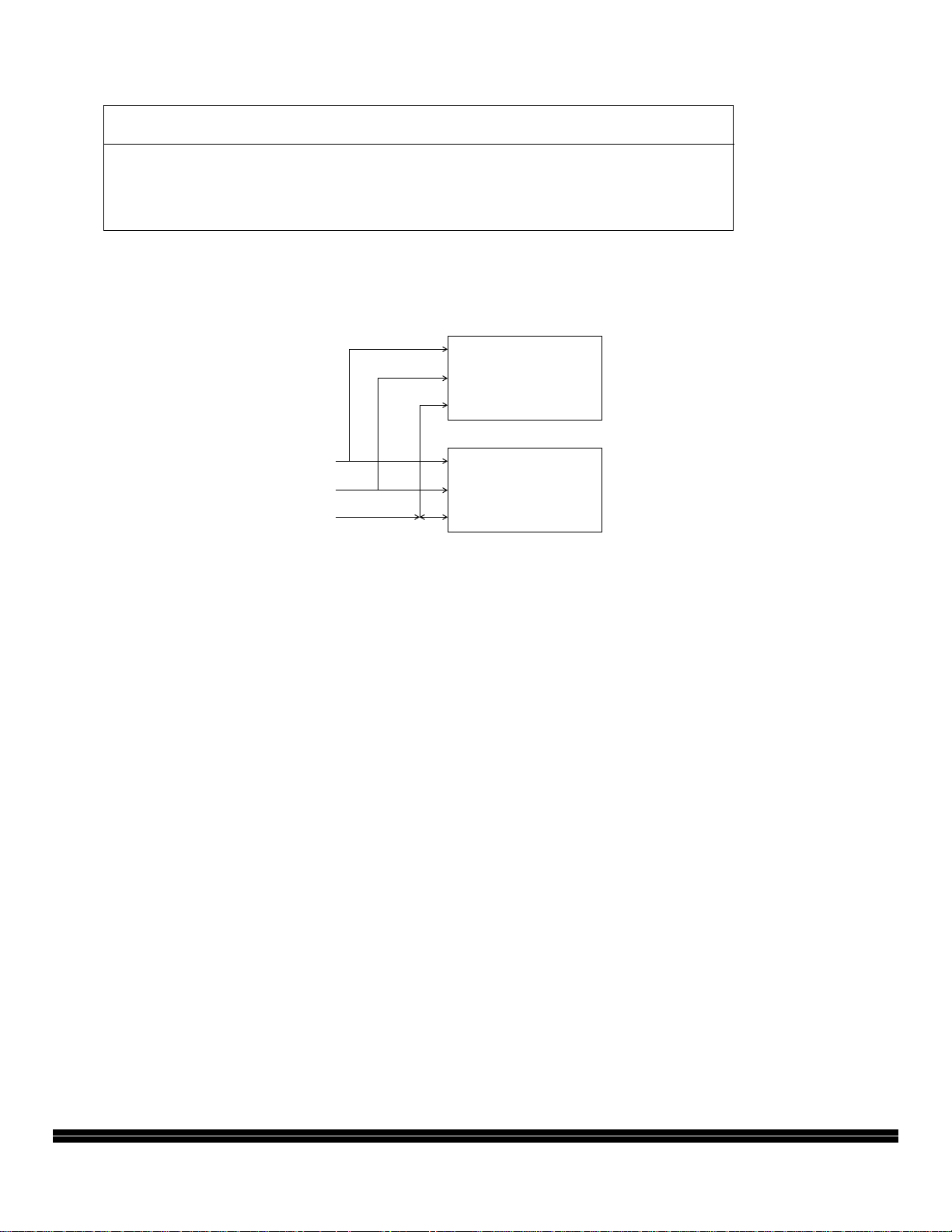
Memory Spaces Mapped To Memory Space Changes
SF1 SF0 Same Physical Address Detected as Faults
0 0 PXY share same addresses none
0 1 PY share same addresses P → X,X → P,X → Y,Y → X
1 0 XY share same addresses P → X,X → P,P → Y,Y → P
1 1 none, all addresses unique P → X,X → P,X → Y,Y → X,P → Y,Y → P
Figure 7-4a. Memory Space Change Detection
—
DATA
PROGRAM
SF1
Address
Data
A
D
CE
A
D
Figure 7-4b. Using SF1 to Physically separate Data and Program Spaces
If the current bus cycle is in an enabled memory space, the —T–T pin is controlled by comparison of the
current bus cycle and the previously latched bus cycle and the current bus cycle information (A, S) is latched
at the end of the bus cycle. Thus the current bus cycle information becomes the previously latched bus cycle
information for comparison in the next enabled external bus cycle. The encoding of the memory space enables is shown in Figure 7-5.
The page circuit normally monitors addresses intended for one external physical memory. However, if multiple memory spaces are mapped into one physical memory at either the same or different addresses, then
the page circuit must monitor multiple memory spaces. These memory space enable bits allow the user to
indicate which memory spaces should be monitored. Also if multiple memory spaces are mapped into different physical memories which are not accessed in an "interleaved" manner, one page circuit can serve
multiple external physical memories by being enabled for more than one memory space. Non-interleaved
accesses with multiple external physical memories are typical of systems where the main external bus activity is block-oriented DMA transfers.
If all three memory space enable bits are cleared, the page circuit is in the Personal Reset state. While in
the Personal Reset state, the page circuit is inactive, —T–T remains deasserted for all external bus cycles,
and no bus cycle information is latched. The first bus cycle after re-enabling the page circuit always has
T–T deasserted since no previous bus cycle information is available for comparison.
—
MOTOROLA DSP96002 USER’S MANUAL 7 - 7
Page 94

—T–T Pin Activity for Current Bus Cycle Latched for
PE XE YE P Space X Space Y Space P Space X Space Y Space
0 0 0 Deasserted Deasserted Deasserted No No No
0 0 1 Deasserted Deasserted Active No No Yes
0 1 0 Deasserted Active Deasserted No Yes No
0 1 1 Deasserted Active Active No Yes Yes
1 0 0 Active Deasserted Deasserted Yes No No
1 0 1 Active Deasserted Active Yes No Yes
1 1 0 Active Active Deasserted Yes Yes No
1 1 1 Active Active Active Yes Yes Yes
Figure 7-5. Memory Space Enables Encoding
7.2.2.2 Refresh Faults
There is no internal support for refresh timers, refresh address counters or refresh faults which should deassert —T–T. The page circuit assumes that refresh does not exist and therefore —T–T must be interpreted
by the external memory controller based on its knowledge of refresh timing and external bus activity. The
use of multiple processors with the same external DRAM/VRAM indicates that the memory controller is the
best place to enforce refresh priorities. With the variety of refresh techniques based on the expected memory activity, the external memory controller state machine is the best place to have global control over refresh timing and arbitration caused by multiple access conflicts. At the end of each external bus cycle, the
external memory controller should determine if it should begin a refresh cycle. If yes, it will disable the trans-
fer acknowledge —T–A signal to ensure that the DSP96002 waits if it begins an external access. Once the
refresh is completed, the external memory controller must remember to ignore the —T–T signal for the next
memory cycle so that a fast access mode is not used. The external state machine should cancel (ignores)
the effect of the —T–T signal in the next external bus cycle after any hardware refresh operation. Note that
if fast interrupts are used to implement a software refresh, refresh looks like a memory read cycle so no
special treatment of —T–T is needed.
—R—A–
7.2.2.3
Since DRAM/VRAM devices are dynamic, there are maximum limits on the —R—A–S and —C—A–S low
time which must be observed. To effectively use the fast access modes with the DSP96002, the external
S, —C—A–S and SC Timeout Faults
state machine must keep —R—A–S asserted between bus cycles for page, nibble and static column
modes. —C—A–S must remain asserted between bus cycles for static column mode only. However, if no
external access occurs after the external state machine is ready for a fast access mode, there is a possibility
that —R—A–S or —C—A–S may "timeout". This is because the idle memory state must be "—R—A–S ac-
tive" to use the fast access modes with the DSP96002 non-burst, random address bus cycles. The
DSP96002 does not provide any internal support for —R—A–S or —C—A–S timeouts. The external state
7 - 8 DSP96002 USER’S MANUAL MOTOROLA
Page 95

machine is responsible for ensuring that —R—A–S or —C—A–S timeouts do not occur. Since typical —R
A–S and —C—A–S timeouts are 10-100 µ sec, one of the simplest solutions is to perform a hardware refresh
which deasserts both —R—A–S and —C—A–S. If refresh is performed often enough, —R—A–S and
C—A–S timeout will never happen.
The serial port of VRAM devices is clocked by a serial clock SC. Since the serial shift register is dynamic,
there is a minimum frequency at which the shift register must be clocked to refresh its contents. This frequency is typically about 20 kHz (50 µ sec refresh period). The DSP96002 does not provide any internal support for SC timeouts. The external state machine is responsible for ensuring that SC timeouts do not occur.
If an SC timeout does occur, the external state machine cancels (ignores) the effect of the —T–T signal in
the next external bus cycle to force a reload of the serial shift register. Fortunately, future 1Mbit VRAMs are
being specified with static shift registers so the SC timeout problem should go away.
—
—
7.2.2.4 DMA Accesses
External DMA accesses to P, X or Y memory spaces are normal bus cycles and cannot be distinguished
from CPU read/write cycles. Therefore DMA accesses can use the —T–T pin and do not need any special
treatment by external hardware.
7.2.2.5 Multiple Memory Banks
Multiple memory banks exist when there are more external memories than needed just to cover the 32-bit
data bus size. In this case, the external memory controller typically selects between banks by enabling one
of several row address strobe (—R—A–S) signals or column address strobe (—C—A–S) signals based on
several address lines. Since changes from one memory bank to another will cause a page fault, multiple
memory banks are allowed and no special treatment is required.
7.2.2.6 Multiple Memory Controllers
Multiple memory controllers may exist to support fast access modes with multiple external physical memories. Since the page circuit can monitor multiple memory spaces and detect or ignore changes in memory
spaces, multiple memory controllers are allowed and no special treatment is required.
7.3 EXPANSION PORTS SELECTION
Every memory space (X, Y and P) is divided into 8 equal portions. The division is fixed, that is, the sizes of
the portions are fixed at 0.5 gigawords per portion and the address boundaries are fixed. Each portion of
each memory space may be individually assigned to one of the external expansion ports (Port A or B). The
mapping is controlled by the Port Select Register (PSR).
7.3.1 Port Select Register (PSR)
The Port Select Register is a 32-bit wide read/write register situated in the X I/O memory space. For each
portion of each memory space there is a bit in the Port Select Register (PSR): if the bit is cleared, the respective portion goes thorough Port A, and if the bit is set, then it goes thorough Port B. Any memory seg-
MOTOROLA DSP96002 USER’S MANUAL 7 - 9
Page 96

ment that is defined as internal remains internal. The Port Select Register format is shown in Figure 7-6 and
is described below.
31 24 23 16 15 8 7 0 PSR
X X X X X X X X Y Y Y Y Y Y Y Y P P P P P P P P Port Select
* 7 6 5 4 3 2 1 0 7 6 5 4 3 2 1 0 7 6 5 4 3 2 1 0 Register
X:$FFFFFFFC
* - reserved, read as zeros, should be written with
zeros for future compatibility.
$FFFFFF7F $FFFFFFFF $FFFFFFFF
X7 Y7 P7
$E0000000 $E0000000 $E0000000
X6 Y6 P6
$C0000000 $C0000000 $C0000000
X5 Y5 P5
$A0000000 $A0000000 $A0000000
X4 Y4 P4
$80000000 $80000000 $80000000
X3 Y3 P3
$60000000 $60000000 $60000000
X2 Y2 P2
$40000000 $40000000 $40000000
X1 Y1 P1
$20000000 $20000000 $20000000
X0 Y0 P0
$00000800 $00000800 $00000400
or or or
$00000200 $00000200 $00000000
Note: X and Y Data Memories lowest external address determined by DE bit in the OMR register. P
Memory lowest external address determined by MA, MB and MC bits in the OMR register.
X Y P
Figure 7-6. DSP96002 Port Select Register (PSR)
7.3.1.1 PSR Program Memory Port Select (P0-P7) Bits 0-7
The Program Memory Port Select control bits (P0-P7) determine the assignment of the 8 Program Memory
segments to Port A or B. If the segment bit is cleared, the Program Memory segment is assigned to Port A.
If the segment bit is set, the memory segment is assigned to Port B. The memory segment to control bit
correlation is shown in Figure 7-6. For example, if the P4 bit is set, then all memory traffic for addresses
P:$80000000 to P:$9FFFFFFF will go thorough Port B. During hardware reset, the P0-P7 bits are cleared
if the MODA pin was hold low when negating —R—E—S—E–T. P0-P7 are set if the MODA pin was hold
high when negating —R—E—S—E–T.
7.3.1.2 PSR Y Data Memory Port Select (Y0-Y7) Bits 8-15
The Y Data Memory Port Select control bits (Y0-Y7) determine the assignment of the 8 Y Data Memory segments to Port A or B. If the segment bit is cleared, the Y Data Memory segment is assigned to Port A. If the
segment bit is set, the memory segment is assigned to Port B. The memory segment to control bit correlation is shown in Figure 7-6. For example, if the Y4 bit is set, then all memory traffic for addresses
Y:$80000000 to Y:$9FFFFFFF will go thorough Port B. During hardware reset, the Y0-Y7 bits are cleared.
7 - 10 DSP96002 USER’S MANUAL MOTOROLA
Page 97

7.3.1.3 PSR X Data Memory Port Select (X0-X7) Bits 16-23
The X Data Memory Port Select control bits (X0-X7) determine the assignment of the 8 X Data Memory segments to Port A or B. If the segment bit is cleared, the X Data Memory segment is assigned to Port A. If the
segment bit is set, the memory segment is assigned to Port B. The memory segment to control bit correlation is shown in Figure 7-6. For example, if the X4 bit is set, then all memory traffic for addresses
X:$80000000 to X:$9FFFFFFF will go thorough Port B. During hardware reset, the X0-X7 bits are cleared.
7.3.1.4 PSR Reserved Bits (Bits 24-31)
These reserved bits read as zero and should be written with zero for future compatibility.
7.4 HOST INTERFACES
7.4.1 Introduction
The DSP96002 provides a Host MPU/DMA Interface for each of its ports. The Host MPU/DMA Interface
provides a 32-bit parallel port to a host processor or DMA controller.
These Host Interfaces (HI) are intended to minimize system chip count and "glue" logic in many computer
graphics and other multiprocessing applications. Each HI has its own control, status and data registers and
is treated as memory-mapped I/O by the DSP96002. Each interface has several dedicated interrupt vector
addresses and control bits to enable/disable interrupts. This minimizes the overhead associated with servicing the interface since each interrupt source has its own service routine.
The HI supports operation in a multiprocessor environment with a set of "host functions". The external device invoking these features is called the "host processor" and may be another DSP96002 processor or a
32-bit microprocessor such as the 68020, 68030, 68040 or 88000. Host processors with 32, 24 or 16-bit
data buses may access all status and control bits of the HI. Host processors with an 8-bit data bus should
add additional hardware to be able to access all status and control bits.
The HI functions allow:
• a host processor to transfer data having an arbitrary address to/from the DSP96002 without
using external shared memory.
• a host processor to interrupt the DSP96002 using multiple interrupt vectors without using external shared memory.
• a host processor (with DMA capability) to transfer data blocks to/from the DSP96002 without
using external shared memory.
• an external DMA controller to transfer data blocks to/from the DSP96002 without using external shared memory.
• unbuffered systems with minimum external logic as well as large buffered systems.
The HI connects to the external world thorough the external expansion port and a set of dedicated pins (described in Section 2):
• 32-bit bidirectional data bus D0-D31.
• 5 control lines: R/—W, —H–S, —H–A, —T–S, —H–R.
• address lines A2-A5.
MOTOROLA DSP96002 USER’S MANUAL 7 - 11
Page 98

The HI appears as a memory mapped peripheral occupying 16 locations in the host processor address
space. Separate transmit and receive data registers are double-buffered to allow the DSP96002 and host
processor to efficiently transfer data at high speed. Host processor communication with the HI registers is
accomplished using standard host processor instructions and addressing modes.
Handshake flags are provided for polled or interrupt-driven data transfers with a host processor.
External DMA controllers (e.g. MC68450) are able to perform block data transfers between the DSP96002
HI and the external host processor memory. For this purpose, a "DMA mode" is provided in the HI. In this
mode, the —H–A pin is used to enable access to the transmit/receive registers in the HI, without regard to
the status of the address lines A2-A5.
The host processor can also issue vectored exception requests to the DSP96002 with the host command
feature. The host processor may select any of the 256 DSP96002 exception routines to be executed by writing a vector address register. This flexibility allows the host processor programmer to execute a wide number of preprogrammed functions inside the DSP96002. Host exceptions can allow the host processor to
read or write DSP96002 registers, X, Y, or Program memory locations and perform control and debugging
operations if exception routines are implemented in the DSP96002 to do these tasks.
The DSP96002 views the HI as a memory mapped peripheral occupying four 32-bit words in X data memory
space. The DSP96002 may use the HI as a normal memory-mapped peripheral using standard polled or
interrupt programming techniques.
7.4.2 HI Reset
The HI is affected by the following types of reset:
HW/SW Reset Hardware (HW) reset, generated by asserting the —R—E—S—E–T pin, or Software
(SW) reset, generated by executing the RESET instruction. Status and control bits in
the HI are affected as defined in Figure 7-7 and Figure 7-8.
HOST Reset HI personal reset, generated when the HRES bit in the HCR register is set. Only HI sta-
tus bits are affected as defined in Figure 7-7 and 7-8. Only the DSP96002 may directly
activate the HOST Reset since HRES is located in the DSP96002 side. Note that the
HI remains in this state as long as the HRES bit is set. The HRES bit is not self-clearing.
INIT HI personal reset, generated when the INIT bit in the ICS register is set. Only HI status
bits are affected as defined in Figure 7-7 and Figure 7-8. Note that INIT may selectively
reset the transmit and/or the receive channel(s) according to the state of the TREQ and
RREQ control bits in the ICS register. Also, the INIT bit is self-clearing, in contrast to
the HRES bit which requires an explicit clear operation.
7.4.3 HI Operation During Stop
The host processor is able to read/write the HI registers when the DSP96002 is in the Stop state (see Section 8). If the clock is stopped in the middle of a host processor access, the flag setup and data transfer
across the HI will be frozen. The transfer and flag setup will finish after the clock is restarted.
7 - 12 DSP96002 USER’S MANUAL MOTOROLA
Page 99

If —H–R is used and the host processor reads RX or writes TX when the DSP96002 is in the Stop state,
then —H–R will only be deasserted after exiting the Stop state. .
Register Register HW/SW HOST INIT INIT INIT Comments
Name Contents Reset Reset TREQ=1 TREQ=0 TREQ=1
RREQ=0 RREQ=1 RREQ=1
ICS HMRC 0 0 0 - 0
HRST 1 1 - - DMAE 0 - - - HF3-HF2 0 - - - HF1-HF0 0 - - - HREQ 0 Note 1 1 Note 2 1
INIT 0 - 0 0 0
TYEQ 0 - - - TREQ 0 - 1 0 1
RREQ 0 - 0 1 1
TRDY 1 1 1 - 1
TXDE 1 1 1 - 1
RXDF 0 0 - 0 0
CVR HC 0 - - - -
HV7-HV0 $0E - - - - port A
$0F - - - - port B
IVR IV7-IV0 $0F - - - -
SEM SEM(15-0) $0000 - - - -
Notes:
1. HREQ = TYEQ + TREQ
2. HREQ = (TYEQ & TRDY) + (TREQ & TXDE)
Symbols:
HW - Hardware Reset caused by asserting the external pin —R—E—S—E–T.
SW - Software Reset caused by executing the RESET instruction.
HOST - Host Personal Reset caused when HRES=1.
INIT - Host Personal Reset caused when INIT=1.
"1" - The bit is set.
"0" - The bit is cleared.
"-" - The bit is not affected.
"+" - Logical OR operation.
"&" - Logical AND operation.
Figure 7-7. Host Interface Reset - Host Processor Side
MOTOROLA DSP96002 USER’S MANUAL 7 - 13
Page 100

Register Register HW/SW HOST INIT INIT INIT Comments
Name Contents Reset Reset TREQ=1 TREQ=0 TREQ=1
RREQ=0 RREQ=1 RREQ=1
HCR HYWE 0 - - - -
HYRE 0 - - - HXWE 0 - - - HXRE 0 - - - HPWE 0 - - - HPRE 0 - - - HRES 1 1 - - HF3-HF2 0 - - - HCIE 0 - - - HTIE 0 - - - HRIE 0 - - - -
HSR HYWP 0 0 0 - 0
HYRP 0 0 0 - 0
HXWP 0 0 0 - 0
HXRP 0 0 0 - 0
HPWP 0 0 0 - 0
HPRP 0 0 0 - 0
HDMA 0 - - - HF1-HF0 0 - - - HCP 0 - - - HTDE 1 1 - 1 1
HRDF 0 0 0 - 0
Figure 7-8. Host Interface Reset - DSP96002 Side
7.4.4 HI Programming Model
The HI block diagram is shown in Figure 7-9. The HI has two programming models - one for the DSP96002
programmer and one for the external host processor programmer. In most cases, the notation used reflects
the DSP96002 perspective. The HI - DSP96002 Programming Model is shown in Figure 7-10. The HI - External Host Processor Programming Model is shown in Figure 7-11. The HI Interrupt Structure is shown in
Figure 7-13. The DSP96002 has two HIs. The registers of the two HIs are identical except for the addresses.
Their names have an A or B suffix identifying the port they are connected to.
7.4.5 Host Transmit Data Register (HTX) - DSP96002 Side
The Host Transmit register (HTX) is used for DSP96002 to host processor data transfers. The HTX register
is viewed as a 32-bit write-only register by the DSP96002. Writing the HTX register clears HTDE. The
DSP96002 may program the HTIE bit to cause a Host Transmit Data interrupt when HTDE is set. The HTX
register is transferred as 32-bit data to the Receive Register RX if both the HTDE bit and the Receive Data
Full RXDF status bit are cleared. This transfer operation sets RXDF and HTDE.
7 - 14 DSP96002 USER’S MANUAL MOTOROLA
 Loading...