Motorola BUT11AF Datasheet

1
Motorola Bipolar Power Transistor Device Data
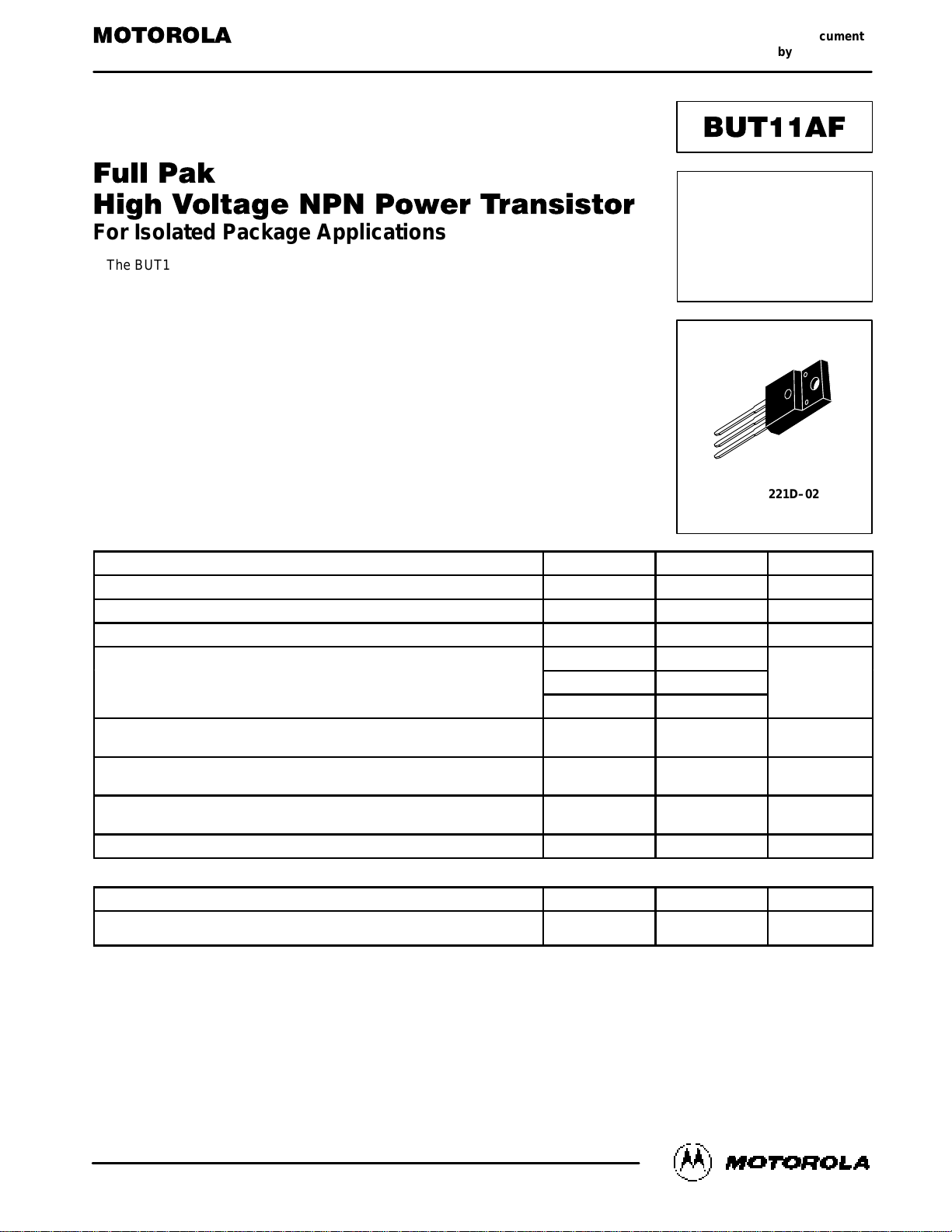
For Isolated Package Applications
The BUT11AF was designed for use in line operated switching power supplies in a
wide range of end use applications. This device combines the latest state of the art
bipolar fabrication techniques to provide excellent switching, high voltage capability
and low saturation voltage.
• 1000 Volt V
CES
Rating
• Low Base Drive Requirements
• Isolated Overmold Package
• Improved System Efficiency
• No Isolating Washers Required
• Reduced System Cost
• High Isolation Voltage Capability (4500 V
RMS
)
MAXIMUM RATINGS
Rating Symbol Value Unit
Collector–Emitter Sustaining Voltage V
CEO(sus)
450 Vdc
Collector–Emitter Breakdown Voltage V
CES
1000 Vdc
Emitter–Base Voltage V
EBO
9.0 Vdc
RMS Isolation Voltage (For 1 sec, Per Figure 7 V
ISOL1
4500
TA = 25°C, Rel. Humidity < 30%) Per Figure 8 V
ISOL2
3500 V
Per Figure 9 V
ISOL3
2500
Collector Current — Continuous
Collector Current — Pulsed (1)
I
C
I
CM
5.0
10
Adc
Base Current — Continuous
Base Current — Pulsed (1)
I
B
I
BM
2.0
4.0
Adc
Total Power Dissipation @ TC = 25°C*
Derated above 25°C
P
D
40
0.32
Watts
W/°C
Operating and Storage Temperature Range TJ, T
stg
– 65 to +150 °C
THERMAL CHARACTERISTICS
Thermal Resistance — Junction to Case* R
θJC
3.125 °C/W
Maximum Lead Temperature for soldering purposes
1/8″ from case for 5 sec.
T
L
260 °C
(1) Pulse Test: Pulse Width = 5.0 ms, Duty Cycle ≤ 10%.
*Measurement made with thermocouple contacting the bottom insulated mounting surface of the package (in a location beneath the die),
the device mounted on a heatsink, thermal grease applied, and a mounting torque of 6 to 8 in . lbs.
Full Pak is a registered trademark of Motorola Inc.
SEMICONDUCTOR TECHNICAL DATA
Order this document
by BUT11AF/D
Motorola, Inc. 1995
POWER TRANSISTOR
5.0 AMPERES
450 VOLTS
40 WATTS
CASE 221D–02
TO–220 TYPE
REV 2

BUT11AF
2
Motorola Bipolar Power Transistor Device Data
ELECTRICAL CHARACTERISTICS
(TC = 25°C unless otherwise noted)
Characteristic
Symbol Min Typ Max Unit
OFF CHARACTERISTICS (1)
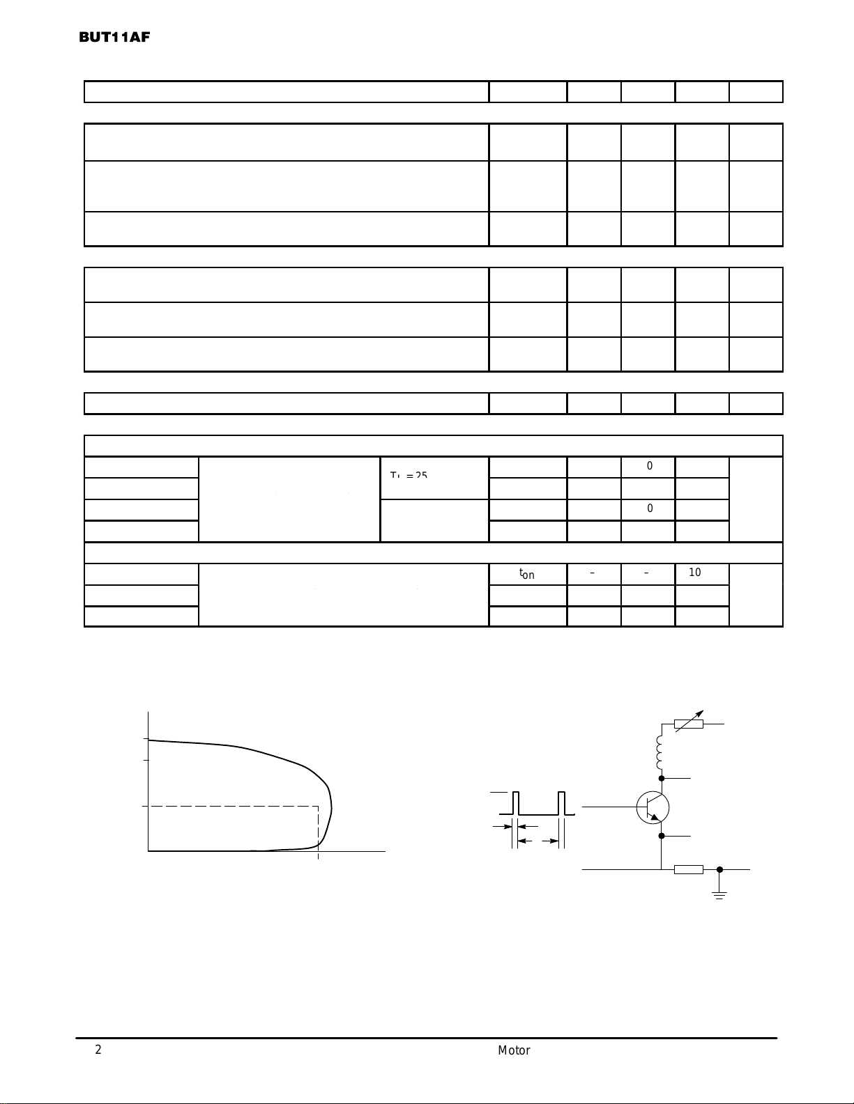
Collector-Emitter Sustaining Voltage (Figures 1 & 2)
(IC = 100 mAdc, IB = 0, L = 25
µH)
V
CEO(sus)
450 – – Vdc
Collector Cutoff Current
(VCE = 1000 Vdc, VBE = 0)
(VCE = 1000 Vdc, VBE = 0, TJ = 125
°C)
I
CES
–
–
–
–
1.0
2.0
mAdc
Emitter-Base Leakage
(VEB = 9.0 Vdc, IC = 0)
I
EBO
– – 10 mAdc
ON CHARACTERISTICS (1)
Collector-Emitter Saturation Voltage
(IC = 2.5 Adc, IB = 0.5 Adc)
V
CE(sat)
– – 1.5 Vdc
Base-Emitter Saturation Voltage
(IC = 2.5 Adc, IB = 0.5 Adc)
V
BE(sat)
– – 1.5 Vdc
DC Current Gain
(IC = 5.0 mAdc, VCE = 5.0 Vdc)
h
FE
10 –
–
–
–
–
DYNAMIC CHARACTERISTICS
Insulation Capacitance (Collector to External Heatsink) Cc-hs – 15 – pF
SWITCHING CHARACTERISTICS
Inductive Load (Figures 3 & 4)
Storage
t
s
– 1100 1400 ns
Fall Time
TJ = 25°C
t
fi
– 80 150
Storage
IC = 2.5 Adc, IB1 = 0.5 Adc
t
s
– 1200 1500
Fall Time
TJ = 100°C
t
fi
– 140 300
Resistive Load (Figures 5 & 6)
Turn-On Time
t
on
– – 1000 ns
Storage Time
t
s
– – 4000
Fall Time t
f
– – 800
(1) Pulse Test: Pulse Width = 300 µs, Duty Cycle ≤ 2.0%.
0
200
250
100
MIN
V
CEO(sus)
VCE (V)
Figure 1. Oscilloscope Display for Sustaining Voltage
I
C
(mA)
HOR.
OSCILLOSCOPE
VERT.
OSCILLOSCOPE
+50 V
L
V
IN
0
t
p
T
100 – 200
Ω
1
Ω
Figure 2. Test Circuit for V
CEO(sus)
IC = 2.5 Adc, IB1 = IB2 = 0.5 Adc
 Loading...