1
Motorola Small–Signal Transistors, FETs and Diodes Device Data
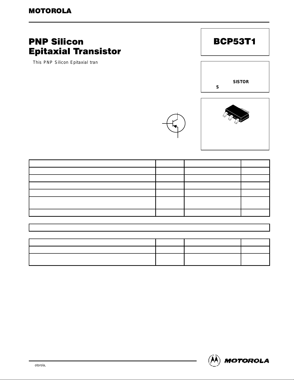
This PNP Silicon Epitaxial transistor i s designed for use in audio amplifier
applications. The device is housed in the SOT-223 package which is designed for
medium power surface mount applications.
• High Current: 1.5 Amps
• NPN Complement is BCP56
• The SOT-223 Package can be soldered using wave or reflow. The formed leads
absorb thermal stress during soldering, eliminating the possibility of damage to
the die
• Available in 12 mm Tape and Reel
Use BCP53T1 to order the 7 inch/1000 unit reel.
Use BCP53T3 to order the 13 inch/4000 unit reel.
MAXIMUM RATINGS
(T
C
= 25°C unless otherwise noted)
Rating Symbol Value Unit
Collector-Emitter Voltage V
CEO
–80 Vdc
Collector-Base Voltage V
CBO
–100 Vdc
Emitter-Base Voltage V
EBO
–5.0 Vdc
Collector Current I
C
1.5 Adc
Total Power Dissipation @ TA = 25°C
(1)
Derate above 25°C
P
D
1.5
12
Watts
mW/°C
Operating and Storage Temperature Range TJ, T
stg
–65 to 150 °C
DEVICE MARKING
AH
THERMAL CHARACTERISTICS
Characteristic Symbol Max Unit
Thermal Resistance — Junction-to-Ambient (surface mounted) R
θJA
83.3 °C/W
Lead Temperature for Soldering, 0.0625″ from case
Time in Solder Bath
T
L
260
10
°C
Sec
1. Device mounted on a glass epoxy printed circuit board 1.575 in. x 1.575 in. x 0.059 in.; mounting pad for the collector lead min. 0.93 sq. in.
Thermal Clad is a trademark of the Bergquist Company
Preferred devices are Motorola recommended choices for future use and best overall value.
Order this document
by BCP53T1/D
SEMICONDUCTOR TECHNICAL DATA
Motorola, Inc. 1996
MEDIUM POWER
PNP SILICON
HIGH CURRENT
TRANSISTOR
SURFACE MOUNT
Motorola Preferred Device
CASE 318E-04, STYLE 1
TO-261AA
1
2
3
4
COLLECTOR 2,4
BASE
1
EMITTER 3
REV 1

BCP53T1
2
Motorola Small–Signal Transistors, FETs and Diodes Device Data
ELECTRICAL CHARACTERISTICS
(T
A
= 25°C unless otherwise noted)
Characteristics
Symbol Min Typ Max Unit
OFF CHARACTERISTICS
Collector-Base Breakdown Voltage (IC = –100 µAdc, IE = 0) V
(BR)CBO
–100 — — Vdc
Collector-Emitter Breakdown Voltage (IC = –1.0 mAdc, IB = 0) V
(BR)CEO
–80 — — Vdc
Collector-Emitter Breakdown Voltage (IC = –100 µAdc, RBE = 1.0 kohm) V
(BR)CER
–100 — — Vdc
Emitter-Base Breakdown Voltage (IE = –10 µAdc, IC = 0) V
(BR)EBO
–5.0 — — Vdc
Collector-Base Cutoff Current (VCB = –30 Vdc, IE = 0) I
CBO
— — –100 nAdc
Emitter-Base Cutoff Current (VEB = –5.0 Vdc, IC = 0) I
EBO
— — –10 µAdc
ON CHARACTERISTICS
DC Current Gain
(IC = –5.0 mAdc, VCE = –2.0 Vdc)
(IC = –150 mAdc, VCE = –2.0 Vdc)
(IC = –500 mAdc, VCE = –2.0 Vdc)
h
FE
25
40
25
—
—
—
—
250
—
—
Collector-Emitter Saturation Voltage (IC = –500 mAdc, IB = –50 mAdc) V
CE(sat)
— — –0.5 Vdc
Base-Emitter On Voltage (IC = –500 mAdc, VCE = –2.0 Vdc) V
BE(on)
— — –1.0 Vdc
DYNAMIC CHARACTERISTICS
Current-Gain — Bandwidth Product
(IC = –10 mAdc, VCE = –5.0 Vdc, f = 35 MHz)
f
T
— 50 — MHz
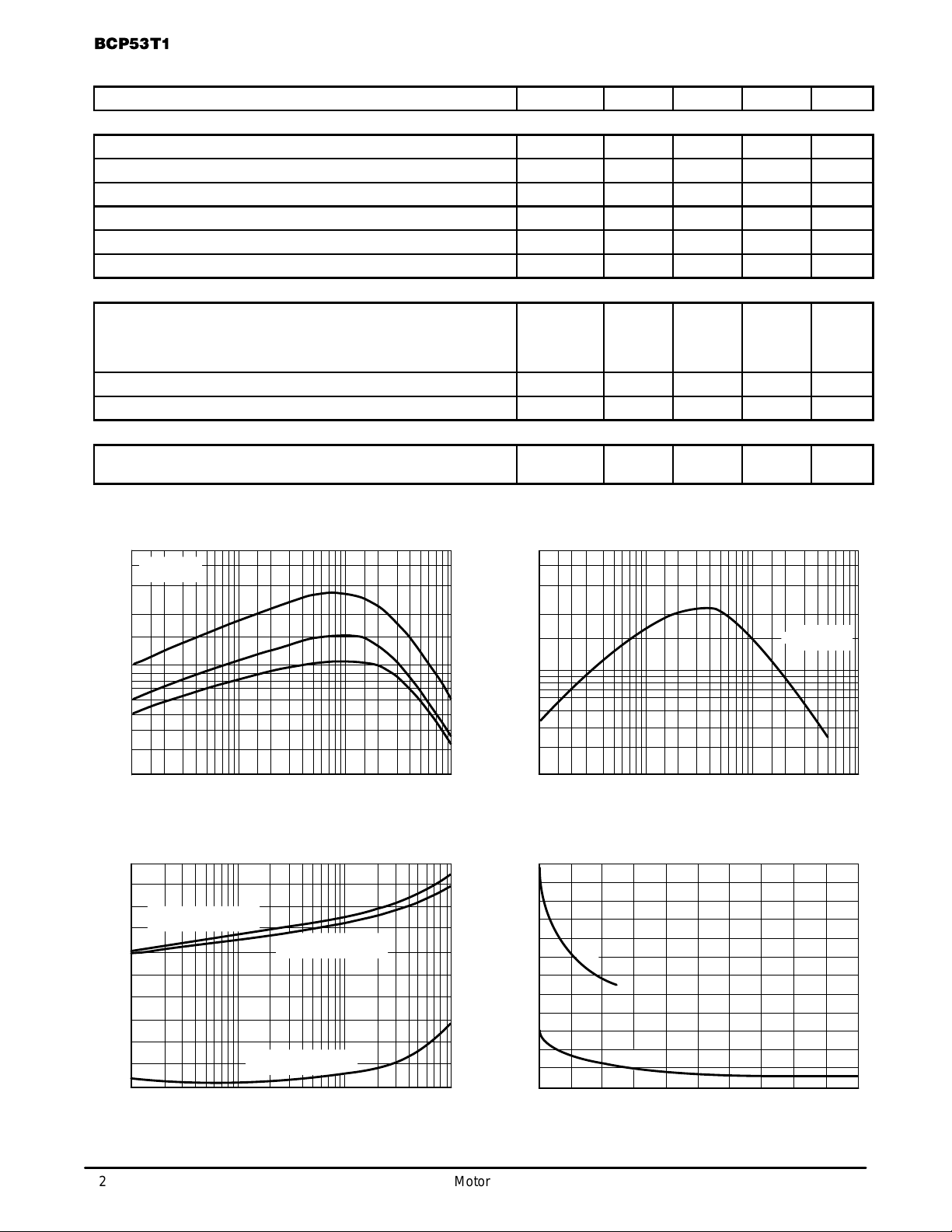
TYPICAL ELECTRICAL CHARACTERISTICS
500
200
100
50
20
1 3 5 10 30 50 100 300 500 1000
IC, COLLECTOR CURRENT (mA)
h , DC CURRENT GAIN
FE
Figure 1. DC Current Gain
IC, COLLECTOR CURRENT (mA)
f , CURRENT GAIN BANDWIDTH PRODUCT (MHz)
T
Figure 2. Current Gain Bandwidth Product
1000
1 10 100
500
300
100
20
50
IC, COLLECTOR CURRENT (mA)
V, VOLTAGE (VOLTS)
Figure 3. Saturation and “ON” Voltages
1000
1
1
0.8
0.6
0.4
0
0.2
10010
120
110
100
90
80
70
60
50
40
30
20
10
0
2018161412108642
0
V, VOLTAGE (VOLTS)
Figure 4. Capacitances
C, CAPACITANCE (pF)
VCE = 2 V
VCE = 2 V
V
(BE)sat
@ IC/IB = 10
V
(BE)on
@ VCE = 2 V
V
(CE)sat
@ IC/IB = 10
C
ib
C
ob
 Loading...