

Page 1

PDR 3500
Transportable Repeater
Basic Service Manual
1
Page 2

2
Page 3

A
Table of Contents
1 - Foreword . . . . . . . . . . . . . . . . . . . . . . . . . . . . . . . . . . . . . . . . . . . . . . . . . . . . . . . . . . . . . . . . . . . . . . . . . . . . . . . 1-1
General . . . . . . . . . . . . . . . . . . . . . . . . . . . . . . . . . . . . . . . . . . . . . . . . . . . . . . . . . . . . . . . . . . . . . . . . . . . . . . . . . 1-1
Safety Information . . . . . . . . . . . . . . . . . . . . . . . . . . . . . . . . . . . . . . . . . . . . . . . . . . . . . . . . . . . . . . . . . . . . . . . . 1-1
Manual Revisions. . . . . . . . . . . . . . . . . . . . . . . . . . . . . . . . . . . . . . . . . . . . . . . . . . . . . . . . . . . . . . . . . . . . . . . . . 1-1
Computer Software Copyrights . . . . . . . . . . . . . . . . . . . . . . . . . . . . . . . . . . . . . . . . . . . . . . . . . . . . . . . . . . . . . . 1-1
Replacement Parts Ordering. . . . . . . . . . . . . . . . . . . . . . . . . . . . . . . . . . . . . . . . . . . . . . . . . . . . . . . . . . . . . . . . . 1-1
Parts Ordering. . . . . . . . . . . . . . . . . . . . . . . . . . . . . . . . . . . . . . . . . . . . . . . . . . . . . . . . . . . . . . . . . . . . . . . . . 1-2
Motorola Parts . . . . . . . . . . . . . . . . . . . . . . . . . . . . . . . . . . . . . . . . . . . . . . . . . . . . . . . . . . . . . . . . . . . . . . . . 1-2
Parts Identification . . . . . . . . . . . . . . . . . . . . . . . . . . . . . . . . . . . . . . . . . . . . . . . . . . . . . . . . . . . . . . . . . . . . . 1-2
Related Documents. . . . . . . . . . . . . . . . . . . . . . . . . . . . . . . . . . . . . . . . . . . . . . . . . . . . . . . . . . . . . . . . . . . . . . . . 1-2
2 - Safety and General Information . . . . . . . . . . . . . . . . . . . . . . . . . . . . . . . . . . . . . . . . . . . . . . . . . . . . . . . . . . . . 2-1
Important Information . . . . . . . . . . . . . . . . . . . . . . . . . . . . . . . . . . . . . . . . . . . . . . . . . . . . . . . . . . . . . . . . . . . . . 2-1
RF Operational Characteristics . . . . . . . . . . . . . . . . . . . . . . . . . . . . . . . . . . . . . . . . . . . . . . . . . . . . . . . . . . . . . . 2-1
Exposure to Radio Frequency Energy . . . . . . . . . . . . . . . . . . . . . . . . . . . . . . . . . . . . . . . . . . . . . . . . . . . . . . . . . 2-1
Electromagnetic Interference/Compatibility . . . . . . . . . . . . . . . . . . . . . . . . . . . . . . . . . . . . . . . . . . . . . . . . . . . . 2-2
3 - Introduction. . . . . . . . . . . . . . . . . . . . . . . . . . . . . . . . . . . . . . . . . . . . . . . . . . . . . . . . . . . . . . . . . . . . . . . . . . . . . 3-1
General . . . . . . . . . . . . . . . . . . . . . . . . . . . . . . . . . . . . . . . . . . . . . . . . . . . . . . . . . . . . . . . . . . . . . . . . . . . . . . . . . 3-1
Compact Mechanical Design . . . . . . . . . . . . . . . . . . . . . . . . . . . . . . . . . . . . . . . . . . . . . . . . . . . . . . . . . . . . . 3-1
State-of-the-Art Electrical Design . . . . . . . . . . . . . . . . . . . . . . . . . . . . . . . . . . . . . . . . . . . . . . . . . . . . . . . . . . . . 3-1
Transmitter Circuitry . . . . . . . . . . . . . . . . . . . . . . . . . . . . . . . . . . . . . . . . . . . . . . . . . . . . . . . . . . . . . . . . . . . 3-1
Receiver Circuitry. . . . . . . . . . . . . . . . . . . . . . . . . . . . . . . . . . . . . . . . . . . . . . . . . . . . . . . . . . . . . . . . . . . . . . 3-1
Station Control Module . . . . . . . . . . . . . . . . . . . . . . . . . . . . . . . . . . . . . . . . . . . . . . . . . . . . . . . . . . . . . . . . . 3-1
Wireline Circuitry. . . . . . . . . . . . . . . . . . . . . . . . . . . . . . . . . . . . . . . . . . . . . . . . . . . . . . . . . . . . . . . . . . . . . . 3-2
Switching Power Supply . . . . . . . . . . . . . . . . . . . . . . . . . . . . . . . . . . . . . . . . . . . . . . . . . . . . . . . . . . . . . . . . 3-2
Standard Features. . . . . . . . . . . . . . . . . . . . . . . . . . . . . . . . . . . . . . . . . . . . . . . . . . . . . . . . . . . . . . . . . . . . . . . . . 3-2
Optional Hardware Features. . . . . . . . . . . . . . . . . . . . . . . . . . . . . . . . . . . . . . . . . . . . . . . . . . . . . . . . . . . . . . . . . 3-2
4 - System Applications . . . . . . . . . . . . . . . . . . . . . . . . . . . . . . . . . . . . . . . . . . . . . . . . . . . . . . . . . . . . . . . . . . . . . . 4-1
Local Control . . . . . . . . . . . . . . . . . . . . . . . . . . . . . . . . . . . . . . . . . . . . . . . . . . . . . . . . . . . . . . . . . . . . . . . . . . . . 4-1
External Duplexer Operation . . . . . . . . . . . . . . . . . . . . . . . . . . . . . . . . . . . . . . . . . . . . . . . . . . . . . . . . . . . . . . . . 4-1
Repeater RA or Cross Band Repeater Operation. . . . . . . . . . . . . . . . . . . . . . . . . . . . . . . . . . . . . . . . . . . . . . . . . 4-1
5 - Models and Specifications . . . . . . . . . . . . . . . . . . . . . . . . . . . . . . . . . . . . . . . . . . . . . . . . . . . . . . . . . . . . . . . . . 5-1
Model Chart . . . . . . . . . . . . . . . . . . . . . . . . . . . . . . . . . . . . . . . . . . . . . . . . . . . . . . . . . . . . . . . . . . . . . . . . . . . . . 5-1
Maintenance Specifications . . . . . . . . . . . . . . . . . . . . . . . . . . . . . . . . . . . . . . . . . . . . . . . . . . . . . . . . . . . . . . . . . 5-2
6 - Approved Accessories. . . . . . . . . . . . . . . . . . . . . . . . . . . . . . . . . . . . . . . . . . . . . . . . . . . . . . . . . . . . . . . . . . . . . 6-1
General . . . . . . . . . . . . . . . . . . . . . . . . . . . . . . . . . . . . . . . . . . . . . . . . . . . . . . . . . . . . . . . . . . . . . . . . . . . . . . . . . 6-1
Antenna . . . . . . . . . . . . . . . . . . . . . . . . . . . . . . . . . . . . . . . . . . . . . . . . . . . . . . . . . . . . . . . . . . . . . . . . . . . . . . . . 6-1
, Motorola, ASTRO, ASTRO CAI, and SECURENET are trademarks of Motorola, Inc.
Commercial, Government, Industrial Solutions Sector
8000 W. Sunrise Blvd., Fort Lauderdale, FL 33322
All Rights Reserved. Printed in U. S. A. 2/2001.
© 2000, 2001 Motorola
68P81093C75-O January 31, 2001 i
Page 4

7 - Setup and Connections . . . . . . . . . . . . . . . . . . . . . . . . . . . . . . . . . . . . . . . . . . . . . . . . . . . . . . . . . . . . . . . . . . . .7-1
Programming with RSS. . . . . . . . . . . . . . . . . . . . . . . . . . . . . . . . . . . . . . . . . . . . . . . . . . . . . . . . . . . . . . . . . . . . .7-1
Introduction . . . . . . . . . . . . . . . . . . . . . . . . . . . . . . . . . . . . . . . . . . . . . . . . . . . . . . . . . . . . . . . . . . . . . . . . . . .7-1
Connecting PC to PDR 3500 RSS Port . . . . . . . . . . . . . . . . . . . . . . . . . . . . . . . . . . . . . . . . . . . . . . . . . . . . . .7-1
Using the RSS . . . . . . . . . . . . . . . . . . . . . . . . . . . . . . . . . . . . . . . . . . . . . . . . . . . . . . . . . . . . . . . . . . . . . . . . .7-2
Hardware Configuration . . . . . . . . . . . . . . . . . . . . . . . . . . . . . . . . . . . . . . . . . . . . . . . . . . . . . . . . . . . . . .7-2
Alignment. . . . . . . . . . . . . . . . . . . . . . . . . . . . . . . . . . . . . . . . . . . . . . . . . . . . . . . . . . . . . . . . . . . . . . . . . .7-2
Channel Information . . . . . . . . . . . . . . . . . . . . . . . . . . . . . . . . . . . . . . . . . . . . . . . . . . . . . . . . . . . . . . . . .7-4
Electrical Connections. . . . . . . . . . . . . . . . . . . . . . . . . . . . . . . . . . . . . . . . . . . . . . . . . . . . . . . . . . . . . . . . . . . . . .7-5
Power Supply Connections . . . . . . . . . . . . . . . . . . . . . . . . . . . . . . . . . . . . . . . . . . . . . . . . . . . . . . . . . . . . . . .7-5
RF Cabling Connections . . . . . . . . . . . . . . . . . . . . . . . . . . . . . . . . . . . . . . . . . . . . . . . . . . . . . . . . . . . . . . . . .7-5
Introduction . . . . . . . . . . . . . . . . . . . . . . . . . . . . . . . . . . . . . . . . . . . . . . . . . . . . . . . . . . . . . . . . . . . . . . . .7-5
Separate RX and TX Connectors. . . . . . . . . . . . . . . . . . . . . . . . . . . . . . . . . . . . . . . . . . . . . . . . . . . . . . . .7-6
Duplexer. . . . . . . . . . . . . . . . . . . . . . . . . . . . . . . . . . . . . . . . . . . . . . . . . . . . . . . . . . . . . . . . . . . . . . . . . . .7-6
8 - Operation . . . . . . . . . . . . . . . . . . . . . . . . . . . . . . . . . . . . . . . . . . . . . . . . . . . . . . . . . . . . . . . . . . . . . . . . . . . . . . .8-1
Description . . . . . . . . . . . . . . . . . . . . . . . . . . . . . . . . . . . . . . . . . . . . . . . . . . . . . . . . . . . . . . . . . . . . . . . . . . . . . .8-1
Summary of Switches, Pushbuttons, and Connectors . . . . . . . . . . . . . . . . . . . . . . . . . . . . . . . . . . . . . . . . . . .8-1
Summary of LED Indicators . . . . . . . . . . . . . . . . . . . . . . . . . . . . . . . . . . . . . . . . . . . . . . . . . . . . . . . . . . . . . .8-1
9 - Troubleshooting . . . . . . . . . . . . . . . . . . . . . . . . . . . . . . . . . . . . . . . . . . . . . . . . . . . . . . . . . . . . . . . . . . . . . . . . . .9-1
Introduction . . . . . . . . . . . . . . . . . . . . . . . . . . . . . . . . . . . . . . . . . . . . . . . . . . . . . . . . . . . . . . . . . . . . . . . . . . . . . .9-1
Troubleshooting Overview . . . . . . . . . . . . . . . . . . . . . . . . . . . . . . . . . . . . . . . . . . . . . . . . . . . . . . . . . . . . . . .9-1
Recommended Test Equipment. . . . . . . . . . . . . . . . . . . . . . . . . . . . . . . . . . . . . . . . . . . . . . . . . . . . . . . . . . . . . . .9-1
Test Equipment List. . . . . . . . . . . . . . . . . . . . . . . . . . . . . . . . . . . . . . . . . . . . . . . . . . . . . . . . . . . . . . . . . . . . .9-1
Troubleshooting Procedures . . . . . . . . . . . . . . . . . . . . . . . . . . . . . . . . . . . . . . . . . . . . . . . . . . . . . . . . . . . . . . . . .9-1
Troubleshooting Overview . . . . . . . . . . . . . . . . . . . . . . . . . . . . . . . . . . . . . . . . . . . . . . . . . . . . . . . . . . . . . . .9-2
Introduction . . . . . . . . . . . . . . . . . . . . . . . . . . . . . . . . . . . . . . . . . . . . . . . . . . . . . . . . . . . . . . . . . . . . . . . .9-2
Procedure 1: Routine Maintenance Functional Checkout . . . . . . . . . . . . . . . . . . . . . . . . . . . . . . . . . . . . .9-2
Procedure 2: Troubleshooting A Reported/Suspected Problem . . . . . . . . . . . . . . . . . . . . . . . . . . . . . . . .9-2
How to Use These Troubleshooting Procedures . . . . . . . . . . . . . . . . . . . . . . . . . . . . . . . . . . . . . . . . . . . . 9-2
Interpreting LED Indicators. . . . . . . . . . . . . . . . . . . . . . . . . . . . . . . . . . . . . . . . . . . . . . . . . . . . . . . . . . . . . . .9-6
Interpreting Alarm Alert Tones . . . . . . . . . . . . . . . . . . . . . . . . . . . . . . . . . . . . . . . . . . . . . . . . . . . . . . . . . . .9-10
Introduction . . . . . . . . . . . . . . . . . . . . . . . . . . . . . . . . . . . . . . . . . . . . . . . . . . . . . . . . . . . . . . . . . . . . . . .9-10
Verifying Transmitter Circuitry. . . . . . . . . . . . . . . . . . . . . . . . . . . . . . . . . . . . . . . . . . . . . . . . . . . . . . . . . . .9-11
Required Test Equipment. . . . . . . . . . . . . . . . . . . . . . . . . . . . . . . . . . . . . . . . . . . . . . . . . . . . . . . . . . . . .9-11
Verifying Transmitter Circuitry Procedure . . . . . . . . . . . . . . . . . . . . . . . . . . . . . . . . . . . . . . . . . . . . . . . 9-11
Verifying Receiver Circuitry. . . . . . . . . . . . . . . . . . . . . . . . . . . . . . . . . . . . . . . . . . . . . . . . . . . . . . . . . . . . .9-15
Required Test Equipment. . . . . . . . . . . . . . . . . . . . . . . . . . . . . . . . . . . . . . . . . . . . . . . . . . . . . . . . . . . . .9-15
Verifying Receiver Circuitry Procedure . . . . . . . . . . . . . . . . . . . . . . . . . . . . . . . . . . . . . . . . . . . . . . . . .9-16
Verifying Receiver Circuitry (Digital-Capable Stations) . . . . . . . . . . . . . . . . . . . . . . . . . . . . . . . . . . . . . . . 9-21
Required Test Equipment. . . . . . . . . . . . . . . . . . . . . . . . . . . . . . . . . . . . . . . . . . . . . . . . . . . . . . . . . . . . .9-22
Wiring Diagram . . . . . . . . . . . . . . . . . . . . . . . . . . . . . . . . . . . . . . . . . . . . . . . . . . . . . . . . . . . . . . . . . . . .9-23
Module Replacement Procedures . . . . . . . . . . . . . . . . . . . . . . . . . . . . . . . . . . . . . . . . . . . . . . . . . . . . . . . . . . . .9-25
General Replacement Information. . . . . . . . . . . . . . . . . . . . . . . . . . . . . . . . . . . . . . . . . . . . . . . . . . . . . . . . .9-25
Anti-Static Precaution . . . . . . . . . . . . . . . . . . . . . . . . . . . . . . . . . . . . . . . . . . . . . . . . . . . . . . . . . . . . . . . . . .9-25
Care of Gold-Plated Connector Contacts. . . . . . . . . . . . . . . . . . . . . . . . . . . . . . . . . . . . . . . . . . . . . . . . . . . .9-26
Power Down Station Before Removing/Inserting Modules . . . . . . . . . . . . . . . . . . . . . . . . . . . . . . . . . . . . .9-26
Validating Repairs . . . . . . . . . . . . . . . . . . . . . . . . . . . . . . . . . . . . . . . . . . . . . . . . . . . . . . . . . . . . . . . . . . . . .9-26
Module Replacement. . . . . . . . . . . . . . . . . . . . . . . . . . . . . . . . . . . . . . . . . . . . . . . . . . . . . . . . . . . . . . . . . . .9-26
Station Control. . . . . . . . . . . . . . . . . . . . . . . . . . . . . . . . . . . . . . . . . . . . . . . . . . . . . . . . . . . . . . . . . . . . .9-27
Physical Replacement of the Station Control Module. . . . . . . . . . . . . . . . . . . . . . . . . . . . . . . . . . . . . . .9-27
After Installing the New Station Control Module . . . . . . . . . . . . . . . . . . . . . . . . . . . . . . . . . . . . . . . . . .9-27
Wireline . . . . . . . . . . . . . . . . . . . . . . . . . . . . . . . . . . . . . . . . . . . . . . . . . . . . . . . . . . . . . . . . . . . . . . . . . . . . .9-28
Physical Replacement of the Wireline Module . . . . . . . . . . . . . . . . . . . . . . . . . . . . . . . . . . . . . . . . . . . .9-28
After Installing the New Wireline Module . . . . . . . . . . . . . . . . . . . . . . . . . . . . . . . . . . . . . . . . . . . . . . .9-29
ASTRO Modem Card/V.24 Interface Card. . . . . . . . . . . . . . . . . . . . . . . . . . . . . . . . . . . . . . . . . . . . . . . . . .9-29
ii January 31, 2001 68P81093C75-O
Page 5

Physical Replacement of the Card . . . . . . . . . . . . . . . . . . . . . . . . . . . . . . . . . . . . . . . . . . . . . . . . . . . . . 9-29
After Installing the New Card. . . . . . . . . . . . . . . . . . . . . . . . . . . . . . . . . . . . . . . . . . . . . . . . . . . . . . . . . 9-29
Receiver . . . . . . . . . . . . . . . . . . . . . . . . . . . . . . . . . . . . . . . . . . . . . . . . . . . . . . . . . . . . . . . . . . . . . . . . . . . . 9-29
Physical Replacement of the Receiver Module . . . . . . . . . . . . . . . . . . . . . . . . . . . . . . . . . . . . . . . . . . . 9-29
After Installing the New Receiver Module. . . . . . . . . . . . . . . . . . . . . . . . . . . . . . . . . . . . . . . . . . . . . . . 9-30
Exciter. . . . . . . . . . . . . . . . . . . . . . . . . . . . . . . . . . . . . . . . . . . . . . . . . . . . . . . . . . . . . . . . . . . . . . . . . . . . . . 9-31
Frequency Band Considerations. . . . . . . . . . . . . . . . . . . . . . . . . . . . . . . . . . . . . . . . . . . . . . . . . . . . . . . 9-31
Physical Replacement of the Exciter Module. . . . . . . . . . . . . . . . . . . . . . . . . . . . . . . . . . . . . . . . . . . . . 9-31
After Installing the New Exciter Module . . . . . . . . . . . . . . . . . . . . . . . . . . . . . . . . . . . . . . . . . . . . . . . . 9-31
Power Amplifier. . . . . . . . . . . . . . . . . . . . . . . . . . . . . . . . . . . . . . . . . . . . . . . . . . . . . . . . . . . . . . . . . . . . . . 9-32
Frequency Band Considerations. . . . . . . . . . . . . . . . . . . . . . . . . . . . . . . . . . . . . . . . . . . . . . . . . . . . . . . 9-32
Physical Replacement of the Power Amplifier. . . . . . . . . . . . . . . . . . . . . . . . . . . . . . . . . . . . . . . . . . . . 9-32
After Installing the New Power Amplifier . . . . . . . . . . . . . . . . . . . . . . . . . . . . . . . . . . . . . . . . . . . . . . . 9-33
Power Supply . . . . . . . . . . . . . . . . . . . . . . . . . . . . . . . . . . . . . . . . . . . . . . . . . . . . . . . . . . . . . . . . . . . . . . . . 9-33
Physical Replacement of the Power Supply. . . . . . . . . . . . . . . . . . . . . . . . . . . . . . . . . . . . . . . . . . . . . . 9-33
Backplane . . . . . . . . . . . . . . . . . . . . . . . . . . . . . . . . . . . . . . . . . . . . . . . . . . . . . . . . . . . . . . . . . . . . . . . . . . . 9-34
Before Installing the New Backplane. . . . . . . . . . . . . . . . . . . . . . . . . . . . . . . . . . . . . . . . . . . . . . . . . . . 9-34
Physical Replacement of the Backplane. . . . . . . . . . . . . . . . . . . . . . . . . . . . . . . . . . . . . . . . . . . . . . . . . 9-34
After Installing the New Power Amplifier . . . . . . . . . . . . . . . . . . . . . . . . . . . . . . . . . . . . . . . . . . . . . . . 9-35
Preselector Field Tuning Procedure. . . . . . . . . . . . . . . . . . . . . . . . . . . . . . . . . . . . . . . . . . . . . . . . . . . . . . . . . . 9-35
Required Test Equipment. . . . . . . . . . . . . . . . . . . . . . . . . . . . . . . . . . . . . . . . . . . . . . . . . . . . . . . . . . . . . . . 9-36
VHF Tuning Procedure . . . . . . . . . . . . . . . . . . . . . . . . . . . . . . . . . . . . . . . . . . . . . . . . . . . . . . . . . . . . . . . . 9-36
Calculating Proper Alignment Frequency . . . . . . . . . . . . . . . . . . . . . . . . . . . . . . . . . . . . . . . . . . . . . . . 9-36
Preparing Equipment . . . . . . . . . . . . . . . . . . . . . . . . . . . . . . . . . . . . . . . . . . . . . . . . . . . . . . . . . . . . . . . 9-37
VHF Tuning Procedure. . . . . . . . . . . . . . . . . . . . . . . . . . . . . . . . . . . . . . . . . . . . . . . . . . . . . . . . . . . . . . 9-38
UHF Tuning Procedure . . . . . . . . . . . . . . . . . . . . . . . . . . . . . . . . . . . . . . . . . . . . . . . . . . . . . . . . . . . . . . . . 9-39
Calculating Proper Alignment Frequency . . . . . . . . . . . . . . . . . . . . . . . . . . . . . . . . . . . . . . . . . . . . . . . 9-39
Preparing Equipment . . . . . . . . . . . . . . . . . . . . . . . . . . . . . . . . . . . . . . . . . . . . . . . . . . . . . . . . . . . . . . . 9-40
Tuning Procedure . . . . . . . . . . . . . . . . . . . . . . . . . . . . . . . . . . . . . . . . . . . . . . . . . . . . . . . . . . . . . . . . . . 9-41
10 - Functional Theory of Operation . . . . . . . . . . . . . . . . . . . . . . . . . . . . . . . . . . . . . . . . . . . . . . . . . . . . . . . . . . 10-1
Transmitter Circuitry Operation. . . . . . . . . . . . . . . . . . . . . . . . . . . . . . . . . . . . . . . . . . . . . . . . . . . . . . . . . . . . . 10-1
Introduction . . . . . . . . . . . . . . . . . . . . . . . . . . . . . . . . . . . . . . . . . . . . . . . . . . . . . . . . . . . . . . . . . . . . . . . . . 10-1
Exciter Module Operation . . . . . . . . . . . . . . . . . . . . . . . . . . . . . . . . . . . . . . . . . . . . . . . . . . . . . . . . . . . . . . 10-1
Power Amplifier Module Operation. . . . . . . . . . . . . . . . . . . . . . . . . . . . . . . . . . . . . . . . . . . . . . . . . . . . . . . 10-2
Receiver Circuitry . . . . . . . . . . . . . . . . . . . . . . . . . . . . . . . . . . . . . . . . . . . . . . . . . . . . . . . . . . . . . . . . . . . . . . . 10-2
Introduction . . . . . . . . . . . . . . . . . . . . . . . . . . . . . . . . . . . . . . . . . . . . . . . . . . . . . . . . . . . . . . . . . . . . . . . . . 10-2
Receiver Module Operation . . . . . . . . . . . . . . . . . . . . . . . . . . . . . . . . . . . . . . . . . . . . . . . . . . . . . . . . . . . . . 10-2
Station Control Module . . . . . . . . . . . . . . . . . . . . . . . . . . . . . . . . . . . . . . . . . . . . . . . . . . . . . . . . . . . . . . . . . . . 10-3
Introduction . . . . . . . . . . . . . . . . . . . . . . . . . . . . . . . . . . . . . . . . . . . . . . . . . . . . . . . . . . . . . . . . . . . . . . . . . 10-3
Station Control Module Operation. . . . . . . . . . . . . . . . . . . . . . . . . . . . . . . . . . . . . . . . . . . . . . . . . . . . . . . . 10-3
Wireline Interface Board . . . . . . . . . . . . . . . . . . . . . . . . . . . . . . . . . . . . . . . . . . . . . . . . . . . . . . . . . . . . . . . . . . 10-3
Introduction . . . . . . . . . . . . . . . . . . . . . . . . . . . . . . . . . . . . . . . . . . . . . . . . . . . . . . . . . . . . . . . . . . . . . . . . . 10-3
Wireline Interface Board Operation. . . . . . . . . . . . . . . . . . . . . . . . . . . . . . . . . . . . . . . . . . . . . . . . . . . . . . . 10-3
Power Supply Module Operation. . . . . . . . . . . . . . . . . . . . . . . . . . . . . . . . . . . . . . . . . . . . . . . . . . . . . . . . . . . . 10-4
11 - Block Diagram, Schematics, Electrical Parts List, and Circuit Board Detail. . . . . . . . . . . . . . . . . . . . . . 11-1
68P81093C75-O January 31, 2001 iii
Page 6

List of Tables
Table 1: Model Structure . . . . . . . . . . . . . . . . . . . . . . . . . . . . . . . . . . . . . . . . . . . . . . . . . . . . . . . . . . . . . . . . . . . 5-1
Table 2: Options . . . . . . . . . . . . . . . . . . . . . . . . . . . . . . . . . . . . . . . . . . . . . . . . . . . . . . . . . . . . . . . . . . . . . . . . . . 5-2
Table 3: Specifications . . . . . . . . . . . . . . . . . . . . . . . . . . . . . . . . . . . . . . . . . . . . . . . . . . . . . . . . . . . . . . . . . . . . . 5-2
Table 4: Specifications, continued . . . . . . . . . . . . . . . . . . . . . . . . . . . . . . . . . . . . . . . . . . . . . . . . . . . . . . . . . . . . 5-3
Table 5: Switches, Pushbuttons, and Connectors. . . . . . . . . . . . . . . . . . . . . . . . . . . . . . . . . . . . . . . . . . . . . . . . . 8-1
Table 6: Summary of LED Indicators . . . . . . . . . . . . . . . . . . . . . . . . . . . . . . . . . . . . . . . . . . . . . . . . . . . . . . . . . 8-1
Table 7: Switches, Pushbuttons, and LED Indicators . . . . . . . . . . . . . . . . . . . . . . . . . . . . . . . . . . . . . . . . . . . . . 8-2
Table 8: PDR 3500 LED Indicator Functions . . . . . . . . . . . . . . . . . . . . . . . . . . . . . . . . . . . . . . . . . . . . . . . . . . 9-6
Table 9: Motherboard DIP Switch Settings . . . . . . . . . . . . . . . . . . . . . . . . . . . . . . . . . . . . . . . . . . . . . . . . . . . . 9-34
List of Figures
Figure 1. EIA-232 Wiring Diagram . . . . . . . . . . . . . . . . . . . . . . . . . . . . . . . . . . . . . . . . . . . . . . . . . . . . . . . . . . . . 7-1
Figure 2. Switches , Pushbuttons , Connectors, and LED Indicators for PDR 3500 . . . . . . . . . . . . . . . . . . . . . . . 8-2
Figure 3. PDR 3500 Troubleshooting Overview (Procedure 1: Routine Maintenance). . . . . . . . . . . . . . . . . . . . . 9-3
Figure 4. PDR 3500 Troubleshooting Overview
(Procedure 2: Reported or Suspected Problem) . . . . . . . . . . . . . . . . . . . . . . . . . . . . . . . . . . . . . . . . . . . 9-4
Figure 5. PDR 3500 LED Indicators and Front Panel Buttons and Connectors. . . . . . . . . . . . . . . . . . . . . . . . . . . 9-9
Figure 6. Test Equipment Setup for Verifying Transmitter Circuitry . . . . . . . . . . . . . . . . . . . . . . . . . . . . . . . . . 9-12
Figure 7. Test Equipment Setup for Verifying Receiver Circuitry . . . . . . . . . . . . . . . . . . . . . . . . . . . . . . . . . . . 9-17
Figure 8A. Coupled receiver connection. (Top) B. Coupled duplexer connection. (Bottom) . . . . . . . . . . . . . . . . 9-19
Figure 9. Disabling the Transmitter . . . . . . . . . . . . . . . . . . . . . . . . . . . . . . . . . . . . . . . . . . . . . . . . . . . . . . . . . . . 9-20
Figure 10. Interconnect Diagram . . . . . . . . . . . . . . . . . . . . . . . . . . . . . . . . . . . . . . . . . . . . . . . . . . . . . . . . . . . . . . 9-24
Figure 11. Chassis Ground Wiring Diagram . . . . . . . . . . . . . . . . . . . . . . . . . . . . . . . . . . . . . . . . . . . . . . . . . . . . . 9-25
Figure 12. Test Equipment Setup for Preselector Field Tuning. . . . . . . . . . . . . . . . . . . . . . . . . . . . . . . . . . . . . . . 9-38
Figure 13. Location of Tuning Screws and Cavity Probe Holes . . . . . . . . . . . . . . . . . . . . . . . . . . . . . . . . . . . . . . 9-39
Figure 14. Test Equipment Setup for Preselector Field Tuning. . . . . . . . . . . . . . . . . . . . . . . . . . . . . . . . . . . . . . . 9-41
Figure 15. Location of Tuning Screws and Cavity Probe Holes . . . . . . . . . . . . . . . . . . . . . . . . . . . . . . . . . . . . . . 9-42
Figure 16. PDR 3500 Functional Block Diagram . . . . . . . . . . . . . . . . . . . . . . . . . . . . . . . . . . . . . . . . . . . . . . . . . 11-2
Figure 17. PDR 3500 Schematic Sheet 1 . . . . . . . . . . . . . . . . . . . . . . . . . . . . . . . . . . . . . . . . . . . . . . . . . . . . . . . . 11-3
Figure 18. PDR 3500 Schematic Sheet 2 . . . . . . . . . . . . . . . . . . . . . . . . . . . . . . . . . . . . . . . . . . . . . . . . . . . . . . . . 11-4
Figure 19. PDR 3500 Backplane Circuit Board Detail. . . . . . . . . . . . . . . . . . . . . . . . . . . . . . . . . . . . . . . . . . . . . 11-6
Parts Lists
Electrical Parts List: Backplane Circuit Board......................................................................... 11-5
Mechanical Parts List: PLN1681A Main Chassis .................................................................... 11-7
iv January 31, 2001 68P81093C75-O
Page 7

Foreword
General
Safety Information
Manual Revisions
Computer Software Copyrights
1
The information contained in this manual supplement relates to all
PDR 3500s, unless otherwise specified. This manual provides
sufficient information to enable service shop personnel to
troubleshoot and repair a PDR 3500 to the module level.
Before operating a PDR 3500, please read the “Safety Information”
section in the front of this manual.
Changes which occur after this manual is printed are described in
“FMRs.” These FMRs provide complete information on changes,
including pertinent parts list data.
The Motorola products described in this manual may include
copyrighted Motorola computer programs stored in semiconductor
memories or other media. Laws in the United States and other
countries preserve for Motorola certain exclusive rights for
copyrighted computer programs, including the exclusive right to
copy or reproduce in any form the copyrighted computer program.
Accordingly, any copyrighted Motorola computer programs
contained in the Motorola products described in this manual may not
be copied or reproduced in any manner without the express written
permission of Motorola. Furthermore, the purchase of Motorola
products shall not be deemed to grant either directly or by
implication, estoppel, or otherwise, any license under the
copyrights, patents or patent applications of Motorola, except for the
normal non-exclusive royalty free license to use that arises by
operation of law in the sale of a product.
Replacement Parts Ordering
68P81093C75-O December 1, 2000 1-1
When ordering replacement parts or equipment information, the
complete identification number should be included. This applies to
all components, kits, and chassis. If the component part number is
not known, the order should include the number of the chassis or kit
of which it is a part, and sufficient description of the desired
component to identify it.
Page 8

Crystal and channel element orders should specify the crystal or
channel element type number, crystal and carrier frequency, and the
model number in which the part is used.
Parts Ordering
Motorola Parts
7:00 A. M. to 7:00 P. M. (Central Standard Time)
Monday through Friday (Chicago, U. S. A.)
Domestic (U. S. A.): 1-800-422-420, or 847-538-8023
1-800-826-1913, or 410-712-6200 (Federal Government)
TELEX: 280127
FAX: 1-847-538-8198
FAX: 1-410-712-4991 (Federal Government)
Domestic (U. S. A.) after hours or weekends:
1-800-925-4357
International: 1-847-538-8023
Accessories and Aftermarket Division
(United States and Canada)
Attention: Order Processing
1313 E. Algonquin Road
Schaumburg, IL 60196
Accessories and Aftermarket Division
Attention: International Order Processing
1313 E. Algonquin Road
Schaumburg, IL 60196
Parts Identification
Related Documents
1-847-538-0021 (Voice)
1-847-538-8194 (FAX)
Quantar User’s Guide (Motorola part number 68P81095E05)
RSS User’s Guide (Motorola part number 68P81085E35)
1-2 December 1, 2000 68P81093C75-O
Page 9

•
•
•
•
•
•
•
•
Safety and General Information
Important Information
RF Operational Characteristics
Exposure to Radio Frequency Energy
IMPORTANT INFORMATION ON SAFE AND EFFICIENT
OPERATION. READ THIS INFORMATION BEFORE USING
YOUR TRANSPORTABLE REPEATER.
Your transportable Repeater contains a transmitter and a receiver.
When it is ON, it receives and transmits radio frequency (RF)
energy.
Your Motorola transportable Repeater is designed to comply with
the following national and international standards and guidelines
regarding exposure of human beings to radio frequency
electromagnetic energy:
United States Federal Communications Commission, Code of
Federal Regulations; 47 CFR part 2 sub-part J
2
American National Standards Institute (ANSI) / Institute of
Electrical and Electronic Engineers (IEEE) C95. 1-1992
Institute of Electrical and Electronic Engineers (IEEE) C95.11999 Edition
National Council on Radiation Protection and Measurements
(NCRP) of the United States, Report 86, 1986
International Commission on Non-Ionizing Radiation Protection
(ICNIRP) 1998
National Radiological Protection Board of the United Kingdom
1995
Ministry of Health (Canada) Safety Code 6. Limits of Human
Exposure to Radiofrequency Electromagnetic Fields in the
Frequency Range from 3 kHz to 300 GHz, 1999
Australian Communications Authority Radiocommunications
(Electromagnetic Radiation - Human Exposure) Standard 1999
(applicable to wireless phones only)
68P81093C75-O December 1, 2000 2-1
Page 10

•
•
•
•
•
•
Electromagnetic Interference/ Compatibility
NOTE: Nearly every electronic device is susceptible to
electromagnetic interference (EMI) if inadequately
shielded, designed or otherwise configured for
electromagnetic compatibility.
FACILITIES
To avoid electromagnetic interference and/or compatibility
conflicts, turn off your radio in any facility where posted notices
instruct you to do so. Hospitals or health care facilities may be using
equipment that is sensitive to external RF energy.
FIXED SITE
ANTENNAS
Transportable Repeater equipment is transported to and then set up
at a fixed location and operated as a fixed control station or repeater .
The antenna installation must comply with the following
requirements in order to assure optimal performance and make sure
human exposure to radio frequency electromagnetic energy is within
the guidelines set forth in the above standards:
The antenna must be mounted outside the building.
Mount the antenna on a tower if at all possible. The lo west point
of the antenna must be elevated a minimum of 10 meters above
the ground. This may require the use of a coaxial cable extension
for the antenna.
If the antenna is to be mounted on a building, then it must be
mounted on the roof. If the antenna supplied with the repeater is
used and the repeater cannot be located within the 12 ft. cable
length, then a coaxial cable extension should be used.
As with all fixed site antenna installations, it is the responsibility
of the licensee to manage the site in accordance with applicable
regulatory requirements and may require additional compliance
actions such as site survey measurements, signage, and site
access restrictions in order to insure that exposure limits are not
exceeded.
2-2 December 1, 2000 68P81093C75-O
Page 11

Introduction
General
Compact Mechanical Design
State-of-the-Art Electrical Design
3
The Motorola PDR 3500 provides conventional analog, ASTRO™ ,
ASTRO CAI™ , and SECURENET™ capabilities in a compact,
software-controlled design. The station architecture and
microprocessor-controlled Station Control Module allow for fast
and reliable upgrading. FLASH memory in the Station Control
Module allows software updates to be performed locally (using
serial port), or remotely via modem.
The entire unit is housed in a lockable rugged, black aluminum
extruded case weighing approximately 4l lbs. Internal components
are mounted in a custom, removable chassis, designed to fit a 19"
rack.
Transmitter Circuitry
Receiver Circuitry
Station Control Module
The station transmitter circuitry is designed for 50% duty cycle
operation at full rated power. Output power is continuously
monitored by an internal calibrated wattmeter . The wattmeter output
feeds a power control loop, continually adjusting and maintaining
the desired output power. All adjustments are electronic, including
deviation and output power.
The station receive circuitry features multiple bandwidth capability
(12.5, 25, or 30 kHz, depending on band), as well as ASTRO digital
operation. Injection signals for the 1st and 2nd local mixers are
generated by frequency synthesizer circuitry and are electronically
controlled by the Station Control Module. All receive signals
(analog, SECURENET , ASTRO , and ASTRO CAI ) are detected and
digitized before being sent to the Station Control Module; this
provides improved audio quality , consistent throughout the cov erage
area.
The Station Control Module is microprocessor-based and features
extensive use of ASIC and digital signal processing technology . The
module serves as the main controller for the station, providing signal
processing and operational control for the station modules.
68P81093C75-O December 1, 2000 3-1
Page 12

•
•
•
•
•
•
•
•
•
•
•
Wireline Circuitry
Switching Power Supply
Standard Features
The station wireline circuitry provides a wide variety of telephone
interfaces, including analog, ASTRO , ASTRO CAI , SECURENET ,
Tone Remote Control, and DC Remote Control. Telephone line
connections are easily made to the wireline circuitry via connectors
on the top panel.
The station features a switching-type power supply, accepting a
wide range of A C inputs (85-265 VAC, 49-61 Hz). The po wer supply
generates 13.8 VDC for the station modules.
Compact single case design
Extensive Self-Test Diagnostics and Alarm Reporting
FRU maintenance philosophy
Easily programmed via Radio Service Software
Local or Remote Software downloading to FLASH memory
Upgrades performed by module replacement and/or software
upgrade
Compatible (with appropriate options) with analog,
SECURENET , ASTRO , and ASTRO CAI digital signaling
Optional Hardware Features
Versatile and reliable switching-type power supply
Wide operating temperature range: -30˚ C to + 60˚C (-22˚ F to
+140˚ F)
Duplexer Option – allows a single antenna to serve for both
transmitter and receiver circuitry for repeater applications.
Antenna Relay Option – allows a single antenna to be switched
between transmitter and receiver.
• ASTRO Modem – allows connection (for ASTRO digital
signaling) to a console through a Digital Interface Unit (DIU) in
an ASTRO system, also allows connection to another ASTRO
Modem for digital Cross-Patch.
3-2 December 1, 2000 68P81093C75-O
Page 13

System Applications 4
Local Control The PDR 3500 is an APCO 25 digital repeater. The station is
identical in operation to the Quantar station, hence there is no local
control capability . There is no digital-to-audio translation within the
station. Local control style operation can be accomplished in several
ways:
a. A portable radio may be used as an RF control station talking to
the repeater.
b. The station may be equipped with the wireline and the modem
options and routed through a DIU to a tone remote console. The
T one remote console controls the station via wireline through the
DIU. The wireline in this case is a local 4-wire cable.
External Duplexer Operation
Repeater RA or Cross Band Repeater Operation
The PDR 3500 must be used with an external duplexer when
frequency spacing is less than 3 MHz. The duplexer isolation
required for proper operation is approximately 60 dB. Doubleshielded coaxial cables must be used from the repeater to the
duplexer.
The PDR 3500 can be configured for Repeater RA or cross band
repeater operation by adding the wireline card and the Astro modem
to the each repeater. The repeaters are connected together using the
wireline port on each repeater. The cables are terminated in RJ-45
connectors.
Repeater 1 Repeater 2
Wireline A Wireline A
Wireline B Wireline B
68P81093C75-O December 1, 2000 4-1
Page 14

Notes
4-2 December 1, 2000 68P81093C75-O
Page 15

X
X
X
X
X
X
X
X
X
X
X
X
X
X
Models and Specifications
Model Chart
Table 1: Model Structure
Model Description
P2066B 132-154 MHz
P2067B 150-174 MHz
P2068B 403-433 MHz
P2069B 438-470 MHz
P2070B 470-494 MHz
P2071B 494-512 MHz
Kit Description
PLD1177_ Receiver VHF R1
PLD1178_ Exciter VHF R2
PLD1179_ Receiver VHF R2
PLD1180_ Exciter VHF R2
PLE1254 Receiver UHF R1
PLE1255 Exciter UHF R1
PLE1256 Receiver UHF R2
PLE1257 Exciter UHF R2
PLE1258 Receiver UHF R3
PLE1259 Exciter UHF R3
PLE1260 Receiver UHF R4
PLE1261 Exciter UHF R4
XXXXXX PLN1682_ Board, Control
X X X X X X PLN1681_ Chassis, main
XXXXXX PLN7776_ Case, portable
X X X X X X PLN7777_ Board, backplane
XXXXXX PPN6026_ Power supply
X X
X X
X X
XXXX PFE6060A Duplexer, UHF
X X X X X X PAN6003A Antenna, mag mount
XXXXXX PDR7778A Label
X X X X X X PBN6048A Packing
x = Indicates one of each is required.
PLD7981_ P A, VHF
PLE9367_ PA, UHF R1
PLE9369_ PA, UHF R3
PLE9372_ PA, UHF R4
PFD6060_ Duplexer, VHF
5
68P81093C75-O January 31, 2001 5-1
Page 16

Table 2: Options
OPTION
DESIGNATOR
Q245 Add: Duplexer Adds VHF or UHF duplexer. Requires customer frequency.
Q463 Add: Antenna Relay Adds VHF/UHF antenna relay for base station operation.
Q502 Add: Wireline Adds wireline remote control option.
Q504 Add: ASTRO 9.6 Kbps Modem Adds 9.6 Kbps modem card.
Q661 Add: DC Barry Cable Adds cable with alligator clip for external battery operation.
H338AC Add: Transit Case Adds a transit case for increased protection during transport.
Maintenance
Specifications
DESCRIPTION PURPOSE
The following are the PDR 3500 specifications for analog as
measured per the revised EIA/TIA 603 Standards and for digital as
measured per TIA TSB-102.CAAB:
Table 3: Specifications
GENERAL VHF UHF
Standard model numbers P2066A, P2067A P2068A, P2069A, P2070A, P2071A
Channel spacing 12.5, 25, 30 kHz 12.5, 25 kHz
Stability 0.0001% 0.0001%
Preselector bandwidth (3dB) 7 MHz 7 MHz
Squelch Carrier, PL, DPL Carrier, PL, DPL
Number of modes 1 1
TRANSMITTER VHF UHF
RF power (without duplexer) 30 watts 30 watts
RF power (with duplexer) 20 watts 20 watts
Maximum transmit duty cycle 50% 50%
TX spurs/harmonics -60 dB -60 dB
FM noise (EIA) -45 dB nominal -45 dB nominal
Audio response per EIA per EIA
TX distortion (1 kHz, clear audio) <5% <5%
RECEIVER VHF UHF
Sensitivity (20dBQ) 0.35 uV 0.5 uV
Sensitivity (12dB SINAD) 0.25 uV 0.35 uV
Selectivity (EIA SINAD) 85 dB (25/30 kHz) 85 dB (25 kHz)
75 dB (12.5 kHz) 75 dB (12.5 kHz)
Intermod (EIA SINAD) 80 dB (25/30 kHz)
75 dB (12.5 kHz)
Spurious and image 80 dB 80 dB
Note: Specifications are subject to change without notice.
75 dB
5-2 January 31, 2001 68P81093C75-O
Page 17

Table 4: Specifications, continued
DUPLEXER
Repeat frequency spread, TX/TX: 300 kHz
VHF minimum duplexer T-R separation 3 MHz: 132-174 MHz
UHF minimum duplexer T-R separation 3 MHz: 403-520 MHz
AC power voltage range: 80-265 Vac
AC power frequency input: 49-61 Hz
External DC power: 11-16 Vdc
CURRENT DRAIN
High power repeat: 10.0 A
Standby: 1.9 A
DIMENSIONS
Size (English): 20.00 x 15 x 7.75 inches
Size (metric): 508 X 381 X 197 mm
WEIGHT
Weight (English): 41 lbs
Weight (metric): 18.6 kg
Note: Specifications are subject to change without notice.
68P81093C75-O January 31, 2001 5-3
Page 18

Notes
5-4 January 31, 2001 68P81093C75-O
Page 19

Approved Accessories 6
General The following accessories are recommended by Motorola for use
with the PDR 3500.
Antenna One of the following antennas should be used:
• The magnetic-mount whip antenna (Motorola part number
PAN6003A) shipped with the PDR 3500.
NOTE: This antenna should be cut to frequency before use per the
manufacturer’s instructions enclosed with the antenna.
• An aftermarket antenna which meets these requirements:
- Monopole
- Unity gain
- Tuned to the frequency at which the antenna is to be used
- Minimum input power rating of 60W continuous
- VSWR of 1.5:1 or less
68P81093C75-O September 27, 2000 6-1
Page 20

Notes
Running H/F 6-# September 27, 2000 68P81093C75-O
Page 21

Setup and Connections 7
Programming with RSS
Introduction
Connecting PC to PDR 3500 RSS Port
EIA-232 Female
TXD
RXD
Connects
to COM Port
on PC
GND
RTS
CTS
9-Pin
D-Type
1
2
3
4
5
6
7
8
9
The PDR 3500 uses the same RSS (Radio Service Software) as the
Quantar/Quantro family. Some values shown in RSS screens may
not be valid due to hardware differences between the Quantar
Station and the PDR 3500. A thorough explanation of the
differences will be given in the following sections.
Once the RSS Program has been loaded onto the PC (refer to
Quantar RSS User’s Guide, 68P81085E35), the PC must be
electrically connected to the PDR 3500 via the RSS port located on
the top panel. For this connection, a 9-pin female to 9-pin male EIA232 cable is available (Motorola part number 30-80369E31) from
the Accessories and Aftermarket Product Division (AAD, formerly
known as Motorola National Parts). A cable can also be made using
the wiring diagram in Figure 1.
9-Pin
D-Type
EIA-232 Male
1
TXD
2
RXD
3
4
GND
5
6
RTS
7
CTS
8
9
Connects
to RSS Port
on Top Panel
MAEPF-27075-O
Figure 1. EIA-232 Wiring Diagram
68P81093C75-O December 1, 2000 7-1
Page 22

Connect one end of the cable to COM1 on the PC and the other end
to the 9-pin connector labeled “RSS” on the top panel of the
PDR 3500.
Using the RSS For information on starting the RSS, configuring screen colors,
setting up the PC serial port, and general RSS use, refer to the
Quantar RSS User’s Guide (68P81085E35).
Hardware Configuration From the Main Menu, press “F2-Service. ” Press F2 again to arrive at
the Hardware Configuration Screen.
1. The first field to verify is the Hardware Platform field. The
PDR 3500 is designed using the Quantar profile; it will not
operate properly in any other mode.
2. The next field to verify is the System Type field. This field
should be set to “Conventional.” The PDR 3500 does not operate
as an ASTRO-TAC Receiver or DBS Base Station.
3. Next verify that the Rx Freq Band 1 and Tx Freq Band fields
list the correct ranges for receiver and transmitter.
NOTE: Rx Freq Band 2 should be set to “NONE.”
4. The PA Power Rating field should be set to 25W (low power),
and the Power Supply field should show “AC LOW.” The
PDR 3500 was designed using a Quantar low power station
profile. It will not operate properly using any other
configuration.
5. If the unit is equipped with a Wireline Card, verify that the
Wireline field under the options is set to 4-wire.
Once the Hardware Configuration Screen matches the installed
station hardware, press F8 to validate the configuration. A popup
message will notify the user of any errors in the configuration. For
a complete description of the Hardware Configuration fields,
please refer to the Quantar RSS User’s Guide (68P81085E35).
Alignment From the Main Menu, press “F2-Service. ” No w press “F3” to arri ve
at the Alignment Menu. From this menu, the user may align the RF
Power Out, RSSI, Station Squelch, and BER.
For instructions on performing Rx or Tx Wireline Alignment, please
refer to the Quantar RSS User’s Guide (68P81085E35).
NOTE: Before performing any alignment procedures, first
dekey the station and “Access Disable” the repeater
as shown in step 1 below.
7-2 December 1, 2000 68P81093C75-O
Page 23

1. Access Disable:
1. From the main menu, press “F2-Service.”
2. Press “F6-Status Panel/Software Ver/Set Date and Time.”
3. Press F2 to arrive at the Status Panel Display Screen.
4. From this screen, press F6 to activate the Access Disable
function. In this mode, the station will not keyup in
response to a received signal. To deactivate the Access
Disable function, press shift+F6.
2. RSSI Calibrate:
1. In the Alignment Menu Screen, tab over to the RSSI
Calibrate field, and press F2 to perform the alignment.
2. Using an R2670 or equivalent Communications System
Analyzer, connect the RF out from the Analyzer to the Rx
UHF-type connector on the station top panel.
3. Set the RF output level from the Analyzer to –90 dBm with
no modulation, and set the frequency to PDR 3500 receive
frequency.
4. With the Analyzer RF turned on, make sure the v alue sho wn
in the RSS screen is –90 dBm. If it is not, type in “–90
dBm.”
5. Press F8 to save the calibration.
3. Power Out:
1. In the Alignment Menu Screen, tab over to the Tx Power
field and press F2 to perform the alignment.
2. For this procedure, connect the Tx UHF-type connector on
the station top panel to the RF input of either a Motorola
R-2670 Communications Analyzer, or to the input of an RF
power meter.
3. Press F6 to keyup the station, check the output power level
shown on the R2670 or RF power meter, and press F9 to
dekey the station.
4. Enter the power from the meter in the field shown in the
RSS, then hit F7 for the PDR 3500 to adjust the PA power
output level.
5. Once the unit adjusts the power, again keyup the station,
read the RF power from the meter, dekey the station, enter
the level in the RSS field, and hit F7 again to adjust.
6. Repeat this cycle until the power out is as close to 25 Watts
as possible. If the power output will not adjust properly, hit
F4 to initialize the PA and restart the alignment procedure.
68P81093C75-O December 1, 2000 7-3
Page 24

7. Once the power out is aligned, press F8 to save the settings
to the station codeplug.
4. Squelch:
1. From the Alignment Menu, tab over to the Squelch Adjust
field and press F2 to perform the alignment. The Squelch
control bar is shown in the center of the screen.
2. To open the squelch completely, press F2. To close the
squelch completely, press F4. To adjust the squelch
between fully open and fully closed, use the Pg Up/Pg Dn
keys on the PC.
3. Once the squelch is set, press F8 to save the setting to the
station codeplug.
5. ASTRO Bit Error Report:
1. From the Alignment Menu, tab ov er to the V.52 Rx BER and
RSSI Report, or PROJECT 25 Rx BER and RSSI Report.
2. Connect the R2670 Communications System Analyzer RF
“OUT” port to the Rx UHF-type connector on the station
top panel.
3. Set the generate frequency to the PDR 3500 receive
frequency, and the output level to –113 dBm, with
modulation either V.52 or Project 25 1011 Pattern
generation.
4. Press F2 to perform the alignment. The values for the report
will appear on the RSS screen.
Channel Information From the Main Menu, press F4. Press F4 again to arrive at the
Channel Information Screen. From this screen, the user may
configure the TX/RX frequencies, RF power out, modulation type,
and the various channel traits for up to 16 channels.
1. In this screen, first set the Rx1 and Tx frequency to the proper
values.
NOTE: The Rx2 frequency is set to 0.00000 MHz and cannot
be edited. This is because the PDR 3500 does not
allow for 2 receiv ers. The station will automatically
calculate the Tx Idle Frequency to be the same as the
Tx Frequency.
In most applications, the Tx Idle Frequency should remain the same
as the Tx Frequency. However, in case of portable or mobile radios
unsquelching near the PDR 3500, adjust the Tx Idle frequency to Tx
Frequency -6.25 kHz.
2. Set the modulation type to either Analog, ASTR O, ASTR O CAI,
7-4 December 1, 2000 68P81093C75-O
Page 25

Electrical Connections
Analog/ASTRO CAI, or CAI RX WIDE DEV.
3. Move to page 2 of the Channel Information Screen by pressing
the Pg Dn key. Set the Tx Po wer Out to the desired power lev el.
(The Battery Backup field has no effect on station operation
since there is no battery option for the PDR 3500.)
For a more complete description of the Channel Information fields,
please refer to the Quantar RSS User’s Guide.
Power Supply Connections
RF Cabling Connections
• AC Input Power Connection
Each PDR 3500 is shipped with an eight foot, 3-conductor line
cord. Attach the receptacle end of the cord to the AC input plug
located on the station top panel. Plug the 3-prong plug into a 110
V or 220 V AC grounded outlet.
NOTE: The Power Supply module automatically selects
between 110 V and 220 V.
• DC Input Power Connection
An optional six foot, fused 2-conductor DC power cord is
available. Attach the alligator clip leads (Red “+”, Black “-”) to
an external battery or some other DC source set to +12 V. Plug
the molded connector end to the external DC connector on the
top panel.
NOTE: The top panel external DC connector will not charge
an external battery.
Introduction The transmit and receive antenna RF connections may be made in
one of two fashions depending on the system application.
• Separate TX and RX antennas.
The PDR 3500 top panel has two UHF-type connectors: one for
RX, and one for TX. In this configuration there is a separate
antenna for each connector.
• Duplexer
68P81093C75-O December 1, 2000 7-5
Page 26

Using this configuration, only one antenna is required for both
transmit and receive. The duplexer is mounted to the station top
panel and has a single N-type connector for the antenna. An N-toUHF adapter is provided.
Separate RX and TX Connectors
In order to use two antennas, first disconnect the duplexer (if
equipped). Connect the Rx antenna to the UHF connector labeled
“RX” on the top panel, and the Tx antenna to the UHF connector
labeled “TX” (Figure 2).
Duplexer The duplexer allows the PDR 3500 to use a single antenna for both
transmit and receive.
1. Connect the UHF connector labeled “RX” on the station top
panel, to the N-type connector labeled “RX” on the duplexer.
2. Connect the top panel UHF connector, labeled “TX,” to the Ntype connector labeled “TX” on the duplexer .
3. Connect the antenna UHF-type connector to the connector
labeled “ANT” on the duplexer.
NOTE: To assure optimal performance and that human
exposure to radio frequency electromagnetic energy
is within guidelines, the antenna should be mounted
as described in Section 2, Safety and General
Information, under Fixed Site Antennas.
7-6 December 1, 2000 68P81093C75-O
Page 27

Operation 8
Description This section describes the switches, pushbuttons, connectors, and
LED indicators on the PDR 3500 used during local operation of the
station and servicing.
Summary of Switches, Pushbuttons, and Connectors
Summary of LED Indicators
The following switches, pushbuttons, and connectors allow the
station to be operated or serviced locally. See Figure 2 for the
location and function of these controls and connectors.
Table 5 Switches, Pushbuttons, and Connectors
Top Panel
Wireline connectors Transmit UHF connector
RSS port connector Receive UHF connector
DC connector
AC connector
Momentary PTT/Reset switch
NOTE: Refer to the Troubleshooting section of this manual
for the detailed descriptions and interpretation of the
LED indicators.
The following LED indicators are provided to show the operating
status of the station. See Figure 2 for the location of these indicators.
Table 6 Summary of LED Indicators
Top Panel Station Control Module
Power/Transmit LED Station On
Station Fail
Intcm/Acc D
Control Ch
Rx 1 Active
Rx2 Active
Rx Fail
Aux LED
68P81093C75-O December 1, 2000 8-1
Page 28

Duplexer
Wireline
Connections
(RJ-45)
A
B
C
D
E
Antenna
F
Receive
UHF Jack
Transmit
UHF Jack
MAEPF-27065-O
Figure 2 . Switches , Pushbuttons , Connectors, and LED Indicators for PDR 3500
Table 7 Switches, Pushbuttons, and LED Indicators
Item Name Purpose
A EIA-232 RSS Port Connector Used to connect an IBM® PC (or compatible PC), running
RSS software. Performs station alignment, optimization,
and diagnostics. Requires Null Modem Cable (Motorola part
number 30-80369E31).
B DC Connector External DC source (+12 Vdc)
C AC Connector and Fuses AC Inlet (110/220 Vac, 3 A)
D Power/Transmit LED The function of this LED indicator is described in the Trou-
bleshooting section of this manual.
E Momentary PTT/Reset Switch When set to “PTT,” its purpose is to test the station. When
set to “RESET,” its purpose is to reset the station.
F Control Module Status LEDs The function of these LED indicators is described in the
Troubleshooting section of this manual.
The LED indicators are (from right to left): Station On; Sta-
tion Fail; Intcm/Acc D; Control Ch; Rx 1 Active; Rx2 Active;
Rx Fail; Aux LED.
8-2 December 1, 2000 68P81093C75-O
Page 29

Troubleshooting 9
Introduction This section provides troubleshooting recommendations and
procedures for the PDR 3500 and associated ancillary equipment.
Troubleshooting Overview
Recommended T est Equipment
The troubleshooting procedures and supporting diagrams allow the
service technician to isolate station faults to the module/assembly
level, or to a limited portion of the motherboard circuitry.
The following information is included:
• Alarm indicators and their functions
• Troubleshooting flow charts
• Module replacement procedures
• Post-repair procedures: Performing alignment
after replacing defective modules
Follow this list of recommended test equipment when performing
troubleshooting procedures on the PDR 3500 and ancillary
equipment:
Test Equipment List • Motorola R2001 or R2600 Series
Communications Analyzer (or equivalent)
• PC with RSS program
• In-Line Wattmeter (Motorola S-1350, or
equivalent)
• Dummy Load (50Ω, station wattage or higher)
• Handset/Microphone with PTT switch
(TMN6164, or equivalent)
Troubleshooting Procedures
68P81093C75-O December 1, 2000 9-1
The troubleshooting and repair philosophy employs Field
Replaceable Unit (FRU) substitution. The PDR 3500 is comprised of
self-contained modules (FRUs). Replacing faulty modules should
bring the station back to normal operation.
Page 30

Many of the troubleshooting procedures require the use of the
Motorola-supplied Radio Service Software (RSS) since the PDR
3500 is computer-controlled, employing state-of-the-art signal
processing. The RSS operates on a PC (or compatible), with RS-232
communication port capability. The RSS allows the technician to
access alarm logs, run diagnostics, and set up the equipment for
various audio and RF tests. Complete details on the operation of the
RSS are provided in the RSS User’s Guide (manual number
68P81085E35).
Troubleshooting Overview
Introduction Two procedures are pro vided for troubleshooting the PDR 3500 and
ancillary equipment. Each procedure is designed to quickly identify
faulty modules, and replace them with known working modules.
Procedure 1: Routine Maintenance Functional Checkout
Procedure 2: Troubleshooting A Reported/Suspected Problem
How to Use These Troubleshooting Procedures
Procedure 1 is a series of non-intrusive tests, performed during a
routine maintenance. The technician verifies proper station
operation. An overview of the procedure is shown in the flowchart
(Figure 3).
Procedure 2 should be used when an equipment problem has been
either reported or is suspected. The procedure includes tests that
allow the technician to troubleshoot reported or suspected
equipment malfunctions. An overview of the procedure is shown in
the flow chart (Figure 4).
Perform the following basic steps in order to efficiently troubleshoot
the PDR 3500 equipment.
Step 1. Select the appropriate troubleshooting procedure flow
chart (Procedure 1 or Procedure 2).
Step 2. Perform the selected flow chart tasks. Tasks requiring
additional explanation are marked with page
references.
• Locate the additional information
• Perform the tasks (if any)
• Return to the flow chart
Step 3. Once the faulty module has been identified, proceed to
Module Replacement Procedures, beginning on
page 25.
9-2 December 1, 2000 68P81093C75-O
Page 31
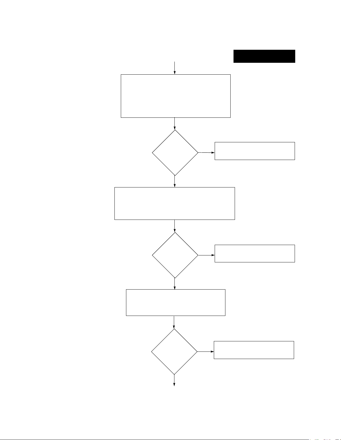
ROUTINE
MAINTENCE VISIT
OBSERVE LED INDICATORS and
MONITOR ALARM TONES (PAGES 6 AND 9)
• OBSERVE LED INDICATORS ON STATION
MODULE FRONT PANELS
• MONITOR ALARM ALERT TONES FROM
EXTERNAL SPEAKER
PROCEDURE 1
MODULE
SUSPECTED
OF BEING
FAULTY?
NO
INTERPRET STATUS REPORT
(RSS USER’S GUIDE–68P81085E35)
• USING RSS, ACCESS THE STATUS REPORT
SCREEN AND LOOK AT HISTORY OF ALARMS
AND TIME STAMPS
MODULE
SUSPECTED
OF BEING
FAULTY?
NO
RUN STATION DIAGNOSTICS
(RSS USER’S GUIDE–68P81085E35)
• USING RSS, RUN DIAGNOSTICS ON
STATION MODULES
YES
YES
GO TO TROUBLESHOO TING
PROCEDURE 2 FLOW CHART
GO TO TROUBLESHOO TING
PROCEDURE 2 FLOW CHART
MODULE
SUSPECTED
OF BEING
FAULTY?
NO
DONE
YES
GO TO TROUBLESHOO TING
PROCEDURE 2 FLOW CHART
Figure 3 PDR 3500 Troubleshooting Overview (Procedure 1: Routine Maintenance)
68P81093C75-O November 30, 2000 9-3
Page 32

REPORTED OR SUSPECTED
PROBLEM
OBSERVE LED INDICATORS and
MONITOR ALARM TONES (PAGES 6 AND 9)
• OBSERVE LED INDICATORS ON STATION
MODULE FRONT PANELS
• MONITOR ALARM ALERT TONES FROM
EXTERNAL SPEAKER
PROCEDURE 2
LED PATTERN
INDICATES STATION
IN SOFTWARE
DOWNLOAD MODE?
NO
MODULE
SUSPECTED
OF BEING
FAULTY?
NO
RUN STATION DIAGNOSTICS
(RSS USER’S GUIDE–68P81085E35)
• USING RSS, ACCESS DIAGNOSTICS SCREEN,
RUN DIAGNOSTICS, AND INTERPRET RESULTS
YES
USING RSS, ACCESS THE STATUS
YES
REPORT SCREEN. ANALYZE
MESSAGES TO DETERMINE IF
MODULE FAILURE HAS OCCURRED.
GO TO MODULE REPLA CEMENT
PROCEDURES ON page 25
MODULE
SUSPECTED
OF BEING
FAULTY?
YES
NO
USING RSS, DOWNLOAD STATION
SOFTWARE TO FLASH MEMORY
ON STATION CONTROL BOARD
MODULE
SUSPECTED
OF BEING
FAULTY?
NO
GO TO
YES
GO TO MODULE REPLACEMENT
PROCEDURES ON page 25
A
Figure 4 PDR 3500 Troubleshooting Overview (Procedure 2: Reported or Suspected Problem)
9-4 December 1, 2000 68P81093C75-O
Page 33

A
CHECK CODE PLUG PROGRAMMING
(RSS USER’S GUIDE – 68P81085E35)
• USING RSS, READ THE STATION CODE PLUG
AND VERIFY THA T PROGRAMMING IS
CORRECT (COMPARE TO CODE PLUG FILE ON
PC FOR PARTICULAR STATION)
PROCEDURE 2
(CONTINUED)
CODE
PLUG
PROGRAMMING
CORRECT?
YES
INTERPRET STATUS REPORT
(RSS USER’S GUIDE–68P81085E35)
• USING RSS, ACCESS THE STATUS REPORT
SCREEN AND LOOK AT HISTORY OF ALARMS
AND TIME STAMPS
MODULE
SUSPECTED
OF BEING
FAULTY?
NO
RUN TRANSMITTER AND RECEIVER TESTS:
• PERFORM VERIFYING TRANSMITTER CIRCUITRY
TESTS (Page 10) TO ISOLATE PROBLEM TO
TRANSMITER CIRCUITRY
• PERFORM VERIFYING RECEIVER CIRCUITRY TESTS
(Page 14) TO ISOLATE PROBLEM TO RECEIVER
CIRCUITRY
• RE-PROGRAM STATION CODE PLUG BY DOWNLOADING
CUSTOMER DATA FROM CODE PLUG FILE FOR
NO
PARTICULAR STATION (RSS GUIDE – 68P81085E35)
• IF PROBLEM STILL EXISTS, PROCEED TO INTERPRET
STATUS REPORT
YES
GO TO MODULE REPLACEMENT
PROCEDURES ON page 25
REPLACE FAULTY MODULE AS
DESCRIBED IN MODULE RELACEMENT
PROCEDURES BEGINNING ON page 25
Figure 4 PDR 3500 Troubleshooting Overview (Procedure 2: Reported or Suspected Problem) (Continued)
68P81093C75-O November 30, 2000 9-5
Page 34

Interpreting LED Indicators
Several LED indicators are provided on the front panels and on the
top panel of the chassis. These LEDs give a quick status indication
of the station equipment. The Station Control Module LEDs are
visible from the station’s top panel. Observing the other LEDs
requires the removal of the station’s chassis from the case. See
Figure 5 for the location of all LED indicators on the station’s
equipment. A listing of each LED indicator , along with a description
of the status indicated by each LED, is shown in Table 8.
Table 8: PDR 3500 LED Indicator Functions
LED Location LED Name Status Definition
Tx Lock – GREEN when Exciter synthesizer is locked; module fully functional.
– OFF when:
synthesizer is out of lock
or
+5V, +14.2V, or both are absent
PA Full – GREEN when transmitter is keyed and PA output power is at expected
power level (as set by technician via RSS during station alignment)
– OFF when:
PA not keyed
or
PA keyed, but PA output power is not at expected power level
(as set by technician via RSS during station alignment)
PA Low – YELLOW when transmitter is keyed and PA output power is less than
expected power level (as set by technician via RSS during station alignment) but
not shut down (for example, during power cutback mode)
– OFF when:
EXCITER MODULE
PA Fail – RED when:
TOP PANEL Pwr/Tx – GREEN when AC or DC input power is present
PA not keyed
or
PA keyed, and PA output power is at expected power level
(as set by technician via RSS during station alignment)
No PA output power (for example, during PA shutdown mode);
LED status is latched, thereby indicating status during current key or
for previous key
NOTE: Any component associated with the PA could cause LED to light.
These include the Exciter, PA, and transmitter circuitry on the backplane.
– FLASHING when PA is in the Test Mode (activated by technician via
RSS; when in Test Mode, power cutback, and open
power loop protection are disabled)
– OFF when PA output power is either at expected level, or at specific
cutback levels (any level other than shutdown); LED status is latched,
thereby indicating status during current key, or for previous key.
– RED when station is transmitting
– OFF when AC or DC input power is absent
9-6 December 1, 2000 68P81093C75-O
Page 35

Table 8: PDR 3500 LED Indicator Functions (Continued)
LED Location LED Name Status Definition
STATION ON – GREEN when SCM fully functional
– FLASHING when front panel switch press detected
– OFF for SCM failure
Station Fail – RED for SCM failure
– OFF when SCM fully functional (no failure)
Intcm/Acc D –YELLOW when station is in Intercom mode
– FLASHING when station is in Access Disable mode
– OFF when station is not in Intercom mode
Control Ch – GREEN when station is control channel (trunking systems only)
– FLASHES each time station decodes IWS (IntelliRepeater systems only)
Rx 1 Active – GREEN when Station Control Board is passing audio/data (receive path unmuted)
from Receiver #1; The following conditions must be met:
Carrier at proper frequency being received
Carrier signal level is above threshold set in codeplug
Squelch criteria met (carrier, PL, DPL,ASTRO, secure, etc.)
(Note that squelch criteria can be manually altered via RSS for
testing purposes)
STATION CONTROL
MODULE (SCM)
Rx 2 Active – Unused in PDR 3500
Rx Fail – RED when receiver is non-functional*
– OFF when above conditions are not met for Receiver #1
– BLINKING ONCE PER SECOND when Receiver #1 is non-functional*
– BLINKING TWICE PER SECOND when Receiver #2 is non-functional* or when
SAM module, or UHSO Module, is non-functional (unused in PDR 3500)
– OFF when RECEIVER is functional* (or no receiver module installed)
*A receive module is considered non-functional if a failure is detected during
diagnostics run at time of power-up, or during normal operation
Aux LED – GREEN LED available for special application function
All LEDs
Flashing On
and Off in
Unison
LEDs
Flashing Up
and Down in
Sequential
Pattern
WL On – GREEN when WIB fully functional
WIRELINE
INTERFACE BOARD
(WIB)
Notes:
1. All LEDs momentarily light following station reset (Volume Up, Volume Down, and Intercom buttons on SCM front panel
pressed simultaneously), or on station power-up.
2. If no LED indicators are on, make sure that AC or DC power to the station power supply is present. If using A C power, check top
panel fuses. Check the circuit breaker at the source. Check the AC or DC line cord. If no problem is found and AC power is used,
suspect the power supply.
Both LEDs
Blinking
Rapidly
– Station is in Software download mode, either initiated by the RSS, or due to
software failure.
– Station received software files from RSS and is in process of downloading the
software to FLASH memory in the Station Control Module
– OFF for WIB failure
– WIB is in Software Download mode (operating software is being downloaded into
the FLASH memory on WIB from Station Control Module)
68P81093C75-O November 30, 2000 9-7
Page 36

9-8 December 1, 2000 68P81093C75-O
Page 37

STATION CONTROL MODULE
(Front Panel - Cover Plate Removed)
Handset
Speaker
RSS Port
Intercom/Shift
CSQ/PL/Off
Vol Down/
Access Disable
Vol Up/Local PTT
Station On
Station Fail
Intrem/AccD
Control Ch
Rx 1 Active
Rx 2 Active
Rx Fail
Aux LED
TOP PANEL
OF STATION
PWR/Tx
PTT/Reset
Switch
WL On
WL Fail
WIRELINE INTERFACE
MODULE
(Front Panel)
Tx Lock
PA Full
PA Low
PA Fail
EXCITER MODULE
(Front Panel)
MAEPF-27030-O
Figure 5 PDR 3500 LED Indicators and Front Panel Buttons and Connectors
68P81093C75-O November 30, 2000 9-9
Page 38
Interpreting Alarm Alert T ones
Introduction Four station alarm conditions are reported with audio alert tones
which are routed to the external speaker connector (RJ-11) on the
front of the control module. (Pin 4 on the RJ-11 is Speaker High; Pin
1 is Speaker Ground.) The alarms are also entered into the alarm log
which can be accessed using the RSS. Refer to the RSS User’s
Guide, part number 68P81085E35.
NOTE: The alarm tones may also be routed to the console
(via the wireline) and transmitted over the air. Refer
to the RSS User’s Guide (part number 68P81085E35)
for details on enabling or disabling these two alarm
routing options.
The four alarm conditions are represented by a series of alarm tones,
from a single beep, to four beeps. Each beep is a 1200 Hz tone,
lasting 125 msec. The alarm tones occur during a repeating 10
second window , with two seconds between successi ve alarms (when
more than one alarm is active). The following two examples
illustrate the timing of the alarm tones.
Example 1: Single Alarm (#3)
beep...beep....beep.................................................................................................[repeats]
Alarm #3
10 Second Window
Example 2: Multiple Alarms (#1 and #4)
beep...........................beep....beep ... beep....beep................................................[repeats]
2 seconds
Alarm #1 Alarm #4
10 Second Window
The alarm tone definitions are as follows:
Number of
Beeps
1 Battery Revert Alarm is reported when station loses AC/DC line power and
2 PA Fail Alarm is reported when PA fails to keyup to full ouput power.
3 Synthesizer Alarm is reported when either Tx or Rx synthesizers fail to
4 Overvoltage Alarm is reported when battery charging voltage is above
Alarm Condition
Name
Alarm Condition Description
reverts to battery backup. Alarm is cleared when station
receives AC/DC power. Should not occur in PDR 3500.
Alarm is cleared upon successful keyup to full power.
lock. Alarm is cleared when both sythesizers lock.
+34.5 V (100 W stations), or +17.25 V (20 W stations). Alarm
is cleared when voltage returns to normal range.
9-10 December 1, 2000 68P81093C75-O
Page 39

V erifying Transmitter Circuitry
Introduction
While most module faults can be detected by running the station
diagnostics provided by the RSS, the following procedure provides
a more traditional method of troubleshooting the transmitter
circuitry . This procedure is useful in the event that the RSS is not at
hand or for some reason cannot be utilized (PC malfunction, etc.)
This procedure allows the service technician to make minor
adjustments and verify the proper operation of the station transmit
circuitry, including:
• Exciter Module
• Power Amplifier Module
• Power Supply Module
• 2.1 MHz Reference Oscillator Circuitry
• Transmitter-related circuitry on the Station
Control Module (SCM)
In general, the transmitter circuitry is exercised by injecting and
measuring signals using a Motorola R2001 Communications
Analyzer (or equivalent). Measured values outside the acceptable
range indicate a faulty module; values within range verify proper
operation of the above listed modules and circuitry.
Required T est Equipment The following test equipment is required to perform the procedure:
• Motorola R2001 Communications Analyzer (or
equivalent)
• Telephone-style handset with PTT switch
(TMN6164, or equivalent)
• In-line Wattmeter (Motorola Model S-1350, or
equivalent)
• Dummy Load (50Ω, station wattage or higher)
Verifying T ransmitter Circuitry Procedure
Step 1. Connect test equipment by performing Step 1 through
3 shown in Figure 6.
Step 2. Connect handset to RJ-11 connector on SCM front
panel, as shown. The co ver plate o ver the SCM side of
the chassis must be removed to access this connector.
Handset
PTT
Button
MEPF-27031-O
68P81093C75-O November 30, 2000 9-11
Page 40

To
Antenna
If duplexer or antenna relay is used,
connect N-to-N cable from antenna
port to in-line wattmeter, otherwise
2
connect UHF-to-N cable from top
panel transmit jack to in-line wattmeter.
Connect wattmeter to dummy load.
Duplexer or
Antenna Relay
Antenna Port
Disconnect cable from antenna port of
duplexer or antenna relaly. If duplexer
1
or relay not used, disconnect cable
from top panel transmit output port.
Antenna
RF SECTION
COMMUNICATIONS
SYSTEM ANALYZER
RF Port Select Knob
789
456
1023
OSCILLOSCOPE
(Pull Out)
In-line
Wattmeter
Motorola
R2001 Communications
Analyzer
MONITOR
Dummy
Load
Connect antenna to R2001 antenna input.
Be sure to pull RF Port Select Knob
3
out to select antenna rf input.
MAEPF-27032-O
Figure 6 Test Equipment Setup for Verifying Transmitter Circuitry
9-12 December 1, 2000 68P81093C75-O
Page 41

Step 3. Press the PTT button and observe the LED indicators
on the Exciter Module front panel.
• If PA Low or PA Fail LED is lit, suspect the
following:
- Power Amplifier Module failure
- Exciter Module failure
- Loose or bad Exciter-to-PA RF cable
- DIP switches on backplane are set for incorrect
station frequency band. DIP switches should
be set as described in the backplane portion of
the Module Replacement section.
- Faulty forward voltage, control voltage, or
temperature voltage translation circuitry on
backplane.
• If TX Lock LED is off, suspect the following:
- Faulty Station Control Module
- Faulty Exciter Module
- Faulty backplane
Step 4. Measure output power by pressing the PTT button and
observing the reading on the in-line wattmeter.
• If the PA output is not at the proper power (as set
for the particular station), adjust the output power
as described in the Setup and Connections
section of this manual.
• If the station will not output the rated power, and
the output is being measured through a duplexer or
antenna relay, the duplexer could be set for the
incorrect frequency, or it could be malfunctioning,
or the antenna relay could be faulty. Connect the
wattmeter directly to the transmit port (UHF
connector) on the station top panel, bypassing the
duplexer or antenna relay. If the station generates
rated power directly from the PA, suspect the
following:
- Faulty duplexer or transmit frequency
mismatch
- Loose or faulty PA-to-duplexer/antenna relay
cable
- Improperly connected or faulty antenna relay
68P81093C75-O November 30, 2000 9-13
Page 42

If the station still does not generate rated power , suspect the
following:
- Power Amplifier Module failure
- Exciter Module failure
- Loose or faulty Exciter-to-PA RF cable
- Faulty forward voltage or control voltage
translation circuitry on backplane
Step 5. If the PA power out is okay, setup R2001 for
spectrum analyzer display. Press the PTT
button and observe the display. The display
should look similar to:
• If the display shows multiple carriers, evenly
spaced about the station transmit frequency,
suspect a faulty PA module.
• If the display shows a solid carrier, but off
frequency, suspect the following:
- Faulty Exciter or Station Control Module
• If the display shows a single carrier moving
erratically, suspect the following:
- Faulty Station Control Module
- Faulty Exciter Module
- Faulty PA Module
Step 6. If the display is okay, setup R2001 to display
modulation. Using the handset, push the PTT
button and speak into the mouthpiece. Verify
that the display shows:
• If the proper display is not obtained, suspect faulty
SCM or Exciter Module
Step 7. Set the R2001 for GEN/MON MTR. Press the PTT
button and speak loudly into the mouthpiece to cause
maximum deviation. Display should read ±5 kHz
maximum.
• If the proper display is not obtained, suspect faulty
SCM or Exciter Module
Step 8. This completes the Verifying Transmitter Circuitry
test procedure. If all displays and measurements are
correct, the transmitter circuitry may be considered to
be operating properly.
9-14 December 1, 2000 68P81093C75-O
Page 43

• Remove test equipment.
• Restore the station to normal service.
• Return to the trouble shooting flow chart to resume
the troubleshooting sequence.
Verifying Receiver Circuitry
Introduction
While most module faults can be detected by running the station
diagnostics provided by the RSS, the following procedure provides
a more traditional method of troubleshooting the receiver circuitry.
This procedure is useful in the event that the RSS is not at hand, or,
for some reason, cannot be utilized (PC malfunction, etc.)
This procedure allows the service technician to make minor
adjustments and verify the proper operation of the station receive
circuitry, including:
• Receiver Module
• Power Supply Module
• 2.1 MHz Reference Oscillator Circuitry
• Receiver-related circuitry in the Station Control
Module (SCM)
In general, the receiver circuitry is exercised by injecting and
measuring signals using a Motorola R2001 Communications
Analyzer (or equivalent). Measured values outside the acceptable
range indicate a faulty module; values within range verify proper
operation of the above listed modules and circuitry.
Required T est Equipment The following test equipment is required to perform the procedure:
• Motorola R2001 Communications Analyzer (or
equivalent)
• Telephone-style handset with PTT switch
(TMN6164, or equivalent)
• RJ-11 to BNC cable
• Dummy Load (50Ω, station wattage, or higher)
IMPOR
TANT! If the station operates as a repeater, the transmit output from
the station must be connected to a dummy load to prevent overthe-air broadcast during receiver testing.
68P81093C75-O November 30, 2000 9-15
Page 44

Verifying Receiver Circuitry Procedure
Step 1. Connect test equipment by performing Step 1 through
3 shown in Figure 7.
NOTE: The cover plate over the SCM side of the chassis
must be removed to perform these tests.
Step 2. Disable PL and carrier squelch by repeatedly pressing
the PL/CSQ/Off button until receiver noise is heard
through the handset (or external speaker). Refer to
Figure 5 for the location of the PL/CSQ/Off button. If
no audio is heard, suspect the following:
• Faulty Receiver Module
• Faulty Station Control Module
• R2001 is outputting a carrier signal
Step 3. Set R2001 to generate a 0.5 µV (-13 dBm) FM signal
at the PDR 3500 receiver frequency, modulated by a 1
kHz tone at 3 kHz deviation. The 1 kHz tone should be
audible through the handset (or external speaker). If
no audio is heard, suspect the following:
• Faulty Station Control Module (2.1 MHz
reference)
• Faulty Receiver Module
• Faulty antenna-to-Receiver preselector RF cable
• Faulty R2001-to-station RF cable
• Duplexer/station receive frequency mismatch, or
faulty duplexer
9-16 December 1, 2000 68P81093C75-O
Page 45

Disconnect cables from top
panel transmit and
1
receive ports.
To
Antenna
Connect handset to RJ-11 jack on
front panel of Station Control Module
3
(or External Speaker to RJ-11 jack).
RF SECTION
COMMUNICATIONS
SYSTEM ANALYZER
RF In/Out
Connect UHF-to-N cable from station top panel
receive port to R2001 RF in/out. Connect UHF-to-N
2
cable from top panel transmit port to dummy load.
Motorola
R2001 Communications
Analyzer
789
456
1023
MONITOR
OSCILLOSCOPE
Handset
PTT
Button
PDR 3500
Top Panel
Dummy
Load
MAEPF-27033-O
Figure 7 Test Equipment Setup for Verifying Receiver Circuitry
Step 4. If audio is heard, connect the HANDSET RJ-11 jack
to the Oscilloscope input BNC connector, as shown
below.
COMMUNICATIONS
SYSTEM ANALYZER
789
456
1023
RF SECTION
To
Station
Receive
Connector
RJ-11 to BNC Test Cable
Motorola Part No. 01-82069W01
(Available from Motorola WASPD)
OSCILLOSCOPE
Oscilloscope
Input
Station Control
Module
Front Panel
MONITOR
Volume
Up Button
MAEPF-27034-O
68P81093C75-O November 30, 2000 9-17
Page 46

Step 5. Use the Volume Up button to increase the volume to
maximum. Measure the audio level using the R2001.
• Audio level should measure approximately 0.75 to
1.5 V p-p. If not, suspect faulty SCM.
Step 6. Change R2001 injection signal to
• VHF: 0.25 µV (-119 dBm)
• UHF: 0.35 µV (-116 dBm).
Step 7. Measure the receiver 12 dB SINAD sensitivity. The
value should read 12 dB, or greater. If not, tune the
preselector (VHF and UHF only) and re-check 12 dB
SINAD. If 12 dB SINAD cannot be achieved, suspect
the following:
• Damaged cable from top panel receive port to
preselector
• Faulty receiver
• Excessive loss in the R2001-to-station RF cable
NOTE: To measure 12 dB SINAD, the station must be
programmed for mixed mode Analog/Digital
operation. Incorrect reading will result if
programmed for Digital Only operation.
NOTE: For VHF and UHF stations only, refer to
5. Preselector Field Tuning Procedure in this
section. Procedures for tuning the receiver
preselector are described.
Step 8. If the station is configured with a duplexer, continue
with Step 9 to test the duplexer’s performance. If the
station is not configured with a duplexer, go to Step
16.
Step 9. Steps 9 through 13 describe a method of measuring
the effect of insertion loss from the duplexer on
receiver sensitivity. Connect the dummy load to the
station’s top panel receive port through a capacitive
coupler (isolated T). Connect the R2001 to the isolated
side of the coupler. (See Figure 8.)
9-18 December 1, 2000 68P81093C75-O
Page 47

Duplexer
RX
PDR 3500
Top Panel
TX
PDR 3500
Top Panel
Capacitive
Coupler
(Isolated T)
RF SECTION
RF Output
RF SECTION
COMMUNICATIONS
SYSTEM ANALYZER
COMMUNICATIONS
SYSTEM ANALYZER
789
456
1023
OSCILLOSCOPE
R2001 Communications
MAEPF-27035-O
789
456
1023
OSCILLOSCOPE
Motorola
Analyzer
Dummy
Load
MONITOR
MONITOR
Duplexer
RF Output
TX
RX
Capacitive
Coupler
(Isolated T)
Motorola
R2001 Communications
Analyzer
Dummy
Load
MAEPF-27036-O
Figure 8 A. Coupled receiver connection. (Top) B. Coupled duplexer connection. (Bottom)
Step 10. Disable the transmitter by holding the Shift button and
then pressing the Access Disable button on the Station
Control Module, as shown in Figure 9. When the
transmitter is disabled, the yellow Access disable light
on the SCM will flash. This step is very important.
With the transmitter disabled, the PA Full LED on the
Exciter Module should not light, even when the station
is receiving.
68P81093C75-O November 30, 2000 9-19
Page 48

Station Control
Module
Press and hold
1
Shift Button.
Intcm/Acc D LED
3
should Flash yellow.
Press Vol Down/
2
Access Disable
Exciter
Module
Figure 9 Disabling the Transmitter
PA Full LED should
4
NOT illuminate.
MAEPF-27037-O
Step 11. Measure the 12dB SINAD sensitivity and make a note
of the level. This level will serve as a baseline for the
receiver sensitivity. If 12 dB SINAD cannot be
achieved, suspect the following:
• Test configuration used does not match that sho wn
in Figure 8B.
• Excessive loss in the coaxial cables or coupler.
Step 12. Remove the cable connecting the coupler to the top
panel receive port. Connect the coupler to the
duplexer’s antenna port. Connect the duplexer’s
receive port to the station’s top panel receive port, as
in normal station operation. (See Figure 8B.)
Step 13. Measure the 12 dB SINAD once again, and note the
result. The difference between this 12 dB SIN AD le vel
and the level measured in Step 11 reflects the insertion
loss of the duplexer. The difference should be no
greater than approximately
• VHF: 1.3 dB
• UHF: 1.6 dB
If the difference is greater, suspect the following:
• Duplexer receive and transmit ports are reversed
• Loose or damaged cables between the duplexer
and the station
• Station receive frequency does not match the
duplexer receive frequency. Use a different
frequency or replace the duplexer. (Field tuning of
duplexers is not recommended.)
9-20 December 1, 2000 68P81093C75-O
Page 49

Step 14. Steps 14 and 15 will test the effect of duplexer
quieting on receive sensitivity. Re-enable the
transmitter by holding down the Shift button again
and pressing the Access Disable button on the SCM.
The following lights should indicate that the station is
now operating as a repeater:
• Yellow Access Disable light stops flashing
• PA Full LED on the Exciter Module lights when
the station is receiving.
Step 15. Test the 12 dB SINAD sensitivity. Depending on the
duplexer frequency spacing, this level should be no
more than 1 to 2 dB greater than the Step 13 reading
(with the transmitter disabled). If the reading is greater
than 1 to 2 dB, the station transmit frequency does not
match the duplexer receive frequency. Use a different
frequency or replace the duplexer. (Field tuning of
duplexers is not recommended.)
Step 16. If the station is not digital-capable, the Verifying
Receiver Circuitry test procedure is complete. The
receiver circuitry is considered to be operating
properly if all displays and measurements are correct.
Verifying Receiver
Circuitry (DigitalCapable Stations)
1. Remove the test equipment.
2. Restore the station to normal service.
3. Return to the troubleshooting flow chart to resume
the troubleshooting sequence.
If the station is digital-capable, continue with the
Digital Only portion of the Verifying Receiver
Circuitry test procedure.
Introduction
While most module faults can be detected by running the station
diagnostics provided by the RSS, the following procedure provides
a more traditional method of troubleshooting the receiver circuitry.
This procedure allows the service technician to make minor
adjustments and verify the proper operation of the station receive
circuitry, including:
• Receiver Module
• Power Supply Module
• 2.1 MHz Reference Oscillator Circuitry
• Receiver-related circuitry in the Station Control
Module (SCM)
68P81093C75-O November 30, 2000 9-21
Page 50

The transmitter circuitry is exercised by injecting and measuring
signals using a Motorola R2670 Communications Analyzer (or
equivalent), and analyzing the Bit Error Rate using the RSS.
Measured values outside the acceptable range indicate a faulty
module; values within range verify proper operation of the above
modules and circuitry.
Required T est Equipment The following test equipment is required to perform the procedure:
• Motorola R2670 Communications Analyzer with
ASTRO CAI Option (or equivalent)
• PC running Radio Service Software (RSS)
program
• Female N-type to Female N-type coaxial cable
• Dummy Load (50Ω, station wattage, or higher).
Required for repeater stations only.
IMPOR
TANT! If the station operates as a repeater, the transmit output from
the station must be connected to a dummy load to prevent overthe-air broadcast during receiver testing.
Step 1. Proceed to ASTRO Bit Error Rate Report (located in
Chapter 4 of the RSS User’s Guide, part number
68P81085E35). Follow the instructions for setting up
the test equipment and initiating a BER report using
the RSS.
Step 2. If the BER reading is above 5%, suspect the
following:
• Faulty Station Control Module (2.1 MHz
reference)
• Faulty Receiver Module
• Faulty antenna-to-receiver preselector RF cable
• Faulty top panel-to-preselector RF cable
• Faulty R2670-to-station RF cable
Step 3. If you are injecting RF directly into the top panel
receiver port, change the R2670 injection signal level
to:
• VHF: 0.25 µV (-119 dBm)
• UHF: 0.35 µV (-116 dBm)
If you are injecting RF through a duplexer , change the
R2670 injection signal level to:
9-22 December 1, 2000 68P81093C75-O
Page 51

• VHF: 0.29 µV (-117.7 dBm)
• UHF: 0.43 µV (-114.4 dBm)
NOTE: For VHF and UHF stations only, refer to
5. Preselector Field Tuning Procedure in this
section, for procedures to tune the receiver
preselector.
Step 4. Note the receiver BER reading. The BER reading
should be 5% or less. If not, and if a duplexer is being
used, repeat the BER test, bypassing the duplexer. If
the BER is 5% or less after bypassing the duplexer , the
station frequencies do not match the duplexer
frequencies, or the duplexer-to-top panel cables are
faulty.
If the BER, as tested straight into the top panel, is
greater than 5%, tune the preselector and re-check the
BER reading. If a reading of 5%, or less, cannot be
achieved, replace the Receiver Module.
Step 5. This completes the Verifying Receiver Circuitry test
procedure. If all displays and measurements are
correct, the receiver circuitry may be considered to be
operating properly.
1. Remove test equipment.
2. Restore the station to normal service.
3. Return to the trouble shooting flow chart to resume
the troubleshooting sequence.
Wiring Diagram Please refer to Figure 10 for a conceptual line drawing of the
motherboard, modules, and other components set flat outside of the
chassis and properly interconnected.
Please refer to Figure 11 on page 25 for a detailed diagram of the
connections from the AC inlet connector to the power supply and
chassis ground.
68P81093C75-O November 30, 2000 9-23
Page 52

Rx
Power
Supply
AC Jack
DC
B
D
C
SwitchLED
Motherboard
Terminal
Tabs
J20 P10
P5
P9
F
F
G
A
RSS
E
I
H
Tx
Fan Fan
J
MAEPF-27080-O
Receiver
K
Exciter
PA
Figure 10 Interconnect Diagram
Reference From To Description
A Top panel UHF Receiver mini-UHF Receive RF coaxial cable
B Top panel AC connector Power supply terminals H, N, GND 120/240 VAC to power supply
C Power supply terminals POS,
NEG
D Top panel DC connector Backplane terminals BLU, BLK 14 VDC input to station
E Top panel DB-9 connector Backplane connector J20 RSS interface ribbon cable assembly
F Top panel LED/Switch Backplane Molex P5/P9 LED/Switch assembly
G Chassis cooling fans Backplane 3-pin Molex P5 Cooling fan assembly
H Backplane terminals RED,
BLK
I Backplane connector P10 PA Control/feedback ribbon cable
J PA mini-UHF Top panel UHF Transmit RF coaxial cable
K Exciter mini-UHF PA RF drive coaxial cable
Backplane terminals WHT, BLK 14 VDC from power supply
PA 14 VDC input 14 VDC to PA
9-24 December 1, 2000 68P81093C75-O
Page 53

AC Inlet
(Viewed from
Underside)
Power Supply
Output Input
Pos
HN
Neg
BROWN
ORANGE
Nuts
Ring Lugs
Chassis
Ground Stud
GRN/YEL
GRN/YEL
Lock
Washers
Figure 11 Chassis Ground Wiring Diagram
Gnd
MAEPF-27099-O
Module Replacement Procedures
General Replacement Information
WARNING: When wearing a Conductive Wrist Strap, be careful near sources of high voltage.
The good ground provided by the wrist strap will also increase the danger of lethal shock
!
from accidentally touching high voltage sources.
Anti-Static Precaution
Station modules suspected of being faulty must be replaced with
modules known to be in good condition in order to restore the station
to proper operation. The following procedures provide instructions
for replacing each of the station modules and performing any
required post-replacement adjustments or programming.
The station circuitry contains many C-MOS and other staticsensitive devices. When servicing the equipment, you must take
precautionary steps to prevent damage to the modules from static
discharge. Complete information on prevention of static protection
is provided in Motorola publication number 68P81106E84,
available through the Accessories and Aftermarket Division.
Some additional precautions are as follows:
• A wrist strap (Motorola part number RSX4015A,
or equivalent) should be worn while servicing the
equipment to minimize static buildup.
CAUTION: DO NOT insert or remove station modules with power applied. This may result in
damage to the modules.
!
68P81093C75-O November 30, 2000 9-25
Page 54

• Do not insert or remove modules with power
applied. Al w ays turn of f the station by unplugging
the AC and DC cords from the top panel before
inserting or removing modules.
• All spare modules should be kept in a conductive
bag for storage and transporting. When shipping
modules to the repair depot, always pack them in
conductive material.
Care of Gold-Plated Connector Contacts
Power Down Station Before Removing/ Inserting Modules
The connectors between the modules and the station backplane
board are made with gold-plated card edge connector contacts to
provide maximum reliability. Gold-plated materials do not form a
non-conductive oxide layer and therefore should not require
cleaning under normal conditions.
When the modules have been subjected to many e xtraction/insertion
cycles, or if the station is operated in a dusty environment, the
contacts may require cleaning. Do not use an eraser or any type of
abrasive substance to clean either the module card edge connectors,
or the backplane connector contacts.
If the cleaning of gold-plated contacts is required, use a soft cloth
dampened with alcohol to lightly wipe the contacts. Be sure not to
touch the contact surfaces with your fingers; finger oils and salts can
contaminate the contact surfaces.
Before removing or inserting a module into the station chassis and
engaging the backplane connector, be sure to turn off the station
power by unplugging the AC or DC power cord, or both.
Validating Repairs After replacing a faulty module with a module that is known to be in
good condition, perform the following tests to validate the repair.
• If the faulty module was detected as the result of
running station diagnostics via the RSS, run the
diagnostics again after the repair is made to ensure
that the replacement module passes all diagnostic
tests.
• If the faulty module was detected by an
operational failure, perform the operation to
ensure that the repair corrected the reported or
detected failure.
Module Replacement This section discusses the replacement of each of the PDR 3500’s
modules and related requirements and considerations.
9-26 December 1, 2000 68P81093C75-O
Page 55

Station Control Before Removing the Old Station Control Module
A new SCM contains settings in a codeplug (EEPROM). Those
settings can be configured, using the RSS, after the module has been
installed.
If the old SCM is capable of communicating with the RSS, the old
codeplug can be read from the SCM and saved to disk to be
programmed into the new SCM. This is described in the Setup and
Connections section of this manual, and in the RSS User’s Guide
(68P81085E35).
If the old SCM is incapable of communicating with the RSS, an
archival codeplug (one saved on disk) can be used to program the
new SCM. If an archiv al codeplug is una vailable, the new codeplug
will have to be manually configured after installation.
Physical Replacement of the Station Control Module
1. Turn off the station’s power by unplugging the AC and DC
power cords from the top panel.
2. Remove the 8 Phillips screws from the edges of the station’s top
panel and lift the chassis out of the case.
3. Remove the cover plate on the left end of the front of the station
by removing two Torx screws from the front of the plate.
Remove the four Phillips screws from the side and bottom
edges of the plate.
4. Pull out the old Control Module by gripping behind its DB-9,
RJ-11, and RJ-45 connectors, distributing pressure equally
among the connectors.
5. Insert the new module. Make sure it is in the cardguides; push it
firmly into the chassis until it seats into the card-edge
connectors on the backplane. (Do not slam the board against the
backplane or push any harder than necessary to seat the
connectors.)
6. If desired, power up the station while it is still out of the case to
make sure the module is securely in place. If the LEDs do not
light, are dim, or flash rapidly, one or more modules are not
seated properly. Unplug the station before continuing to the
next step.
7. Reassemble the station by reversing steps 2 and 3.
After Installing the New Station Control Module
1. If the codeplug from the old SCM was saved to disk, or if an
archival codeplug exists on disk, it should be programmed into
the new SCM.
68P81093C75-O November 30, 2000 9-27
Page 56

If no preexisting codeplug is available, the new codeplug must
be configured manually using the RSS. See the Setup and
Connections section of this manual or the RSS User’s Guide
(68P81085E35) for details.
2. Perform the following alignment procedures as described in the
RSS User’s Guide (68P81085E35) or the Setup and
Connections section of this manual, or both.
• Reference Oscillator Calibration
• Squelch Adjust
• Power Output
• Tx Deviation Gain Adjust
• Reference Modulation
• RSSI Calibrate
For Wireline-equipped stations only:
• Tx Wireline
• Rx Wireline
Wireline
Physical Replacement of the Wireline Module
For ASTRO stations only:
• Simulcast/ASTRO Launch Time Offset
For 6809 Trunking stations only:
• TDATA
1. Turn off the station’s power by unplugging the AC and DC
power cords from the top panel.
2. Remove the eight Phillips screws from the edges of the station’s
top panel and lift the chassis out of the case.
3. Remove the cover plate on the left end of the front of the station
by removing two Torx screws from the front of the plate.
Remove the four Phillips screws from the side and bottom
edges of the plate.
4. Pull out the old Wireline Module by gripping its front, right
corner (where there are no parts on the board).
5. Set all jumpers on the replacement board to match those on the
faulty board. These include the following:
• Input/ouput impedance matching jumpers
9-28 December 1, 2000 68P81093C75-O
Page 57

• Two-wire/four-wire select jumper
• DC remote control selection jumpers
6. Insert the new module. Make sure it is in the cardguides; push it
firmly into the chassis until it seats into the card-edge
connectors on the backplane. (Do not slam the board against the
backplane or push any harder than necessary to seat the
connectors.)
7. If desired, power up the station while it is still out of the case to
make sure the module is securely in place. The LEDs on the
Wireline should blink rapidly, indicating that firmware is
transferring from the SCM to the Wireline Module. When the
blinking stops, the transfer is complete.
If any of the LEDs do not light or are dim, one or more of the
modules are not seated properly. Unplug the station before
continuing to the next step.
8. Reassemble the station by reversing Steps 2 and 3.
After Installing the New Wireline Module
ASTRO Modem Card/ V.24 Interface Card
Physical Replacement of the Card
After Installing the New Card
Perform the following alignment procedures as described in the RSS
User’s Guide (part number 68P81085E35):
• Rx Wireline
• Tx Wireline
1. Remove the Wireline Module as described above.
2. Unplug the faulty ASTRO Modem Card or the V.24 Interface
Card from the Wireline board by pressing the mounting posts
through the back of the board.
Install the replacement card by pressing it onto the W ireline board
and locking all mounting posts and connectors.
3. Re-install the Wireline Module as described above.
No alignments or adjustments are required. The card is configured
by the Station Control Module on power-up.
Receiver
Physical Replacement of the Receiver Module
68P81093C75-O November 30, 2000 9-29
1. Turn off the station’s power by unplugging the AC and DC
power cords from the top panel.
2. Remove the eight Phillips screws from the edges of the station’s
top panel and lift the chassis out of the case.
Page 58

3. Remove the cover plate on the left end of the front of the station
by removing two Torx screws from the front of the plate.
Remove the four Phillips screws from the side and bottom
edges of the plate. Remove two more Phillips screws from the
bottom of the chassis under the preselector.
4. A coaxial cable runs from the receiver’ s preselector , through the
center wall of the chassis, and to the top panel UHF connector.
Disconnect the cable from the preselector and push the loose end
of the cable through the center wall so that it is completely clear
of the receiver.
5. Pull the old receiver out by gripping the tabs protruding past
each end of the preselector.
6. Insert the new module. Make sure it fits under the metal rails
inside the chassis. Push it firmly into the chassis until it seats
into the card-edge connectors on the backplane. (Do not slam
the board against the backplane or push any harder than
necessary to seat the connectors.)
7. If desired, power up the station while it is still out of the case to
make sure the module is securely in place.
After Installing the New Receiver Module
If any of the LEDs do not light, are dim, or flash rapidly, one or
more of the modules are not seated properly.
8. For VHF and UHF stations, tune the preselector using the
procedure in the Maintenance subsection, Preselector Field
Tuning Procedure. Before continuing to the next step, be sure
to unplug the station.
9. Feed the coaxial cable detached in Step 3 back through the
opening in the center wall of the chassis and reconnect it to the
mini-UHF connector on the preselector.
10. Reassemble the station by reversing Steps 2 and 3.
Perform the following alignment procedures as described in the RSS
User’s Guide (part number 68P81085E35), or in the RSS section of
this manual, or in both:
• Squelch Adjust
• RSSI Calibrate
Preselector tuning is required for proper performance of the
Receiver Module and it should ha ve been performed when installing
the module, as described under “Physical Replacement of the
Receiver Module. ” If the tuning was not performed when the module
was installed, perform it now.
9-30 December 1, 2000 68P81093C75-O
Page 59

Exciter
Frequency Band Considerations
Physical Replacement of the Exciter Module
When replacing the Exciter Module, it is important to remember the
frequency-sensitive nature of the Exciter/Power Amplifier
combination. The Exciter and the PA must match according to the
model breakdown table in this manual. If an Exciter with a new
frequency band is being installed, the corresponding PA must be
installed, as described in the Power Amplifier subsection of “Module
Replacement. ”
1. Turn off the station’s power by unplugging the AC and DC
power cords from the top panel.
2. Remove the eight Phillips screws from the edges of the station’s
top panel and lift the chassis out of the case.
3. Disconnect the coaxial cable running to a mini-UHF connector
at the front of the Exciter.
4. Tilt the chassis up on its back edge; then, from the bottom of the
chassis, remove the six Phillips screws holding the Exciter’s
mounting plate. Slide the mounting plate out of the front of the
chassis.
5. Pull out the old Exciter Module by gripping behind the mini-
UHF connector and pulling gently.
After Installing the New Exciter Module
6. Insert the new module. Make sure it is flat on the bottom of the
chassis. Push it firmly into the chassis until it seats into the cardedge connectors on the backplane. (Do not slam the board
against the backplane or push any harder than necessary to seat
the connectors.)
7. If desired, power up the station while it is still out of the case to
make sure the module is securely in place. If the LEDs do not
light, are dim, or flash rapidly, one or more modules are not
seated properly. Unplug the station before continuing to the
next step.
8. Reassemble the station by reversing Steps 2 through 4.
Perform the following alignment procedures as described in the RSS
User’s Guide (part number 68P81085E35):
• Tx Deviation Gain Adjust
• Reference Modulation
For ASTRO Simulcast systems only:
• ASTRO/Simulcast Launch Time Offset
68P81093C75-O November 30, 2000 9-31
Page 60

Power Amplifier
Frequency Band Considerations
When replacing the Power Amplifier, it is important to remember the
frequency-sensitive nature of the Exciter/Power Amplifier
combination. The Exciter and the PA must match according to the
model breakdown table in this manual. If a PA with a new frequency
band is being installed, the corresponding Exciter must be installed,
as described in the Exciter subsection of “Module Replacement.”
Of equal importance, the PDR 3500 motherboard contains circuitry
which translates between the Exciter from the original Quantar and
the PA from the Spectra™ mobile radio. Since the translations
depend upon the frequency band of the Exciter and the PA, this
circuitry is also frequency-sensitive.
The DIP switches on the motherboard must be set according to the
frequency of the station in order for the proper translation path to be
selected. The DIP switch settings can remain intact if
• The band of the new PA matches the one being
replaced, and
• The Exciter is not being changed.
If the PA band or the Exciter band is being changed, the DIP
switches must be configured to match the new frequency of the PA
and Exciter. Detach the motherboard from the chassis and set the
switches as described in the Backplane subsection of “Module
Replacement.”
Physical Replacement of
the Power Amplifier
1. Turn off the station’s power by unplugging the AC and DC
power cords from the top panel.
2. Remove the eight Phillips screws from the edges of the station’s
top panel and lift the chassis out of the case.
3. Remove the four Phillips screws from the front, right quadrant
of the top panel to release the PA. When removing the fourth
screw, support the PA inside the chassis to prevent it from
falling.
4. Disconnect all four cables between the PA and the station:
a. Unplug the red and black power cable from the PA.
b. Unscrew the mini-UHF connector from the PA.
c. To remove the PA ribbon cable connector, remove the two
Torx screws holding the metal clip over the connector. Pull
the connector loose from the PA.
d. Unscrew the mini-UHF connector on the remaining cable
from the front of the Exciter.
9-32 December 1, 2000 68P81093C75-O
Page 61

5. Reconnect all four cables removed in Step 4. The ribbon cable
connector is keyed so it cannot be attached incorrectly.
Remember to reattach the metal clip over the ribbon cable
connector.
6. Take the sheet of black thermal conductive film that was
between the old PA and the chassis and place it on the new PA.
7. Place the P A in the chassis and line up the scre w holes in the PA
and the thermal film with the holes in the top panel of the
chassis. (It may be useful to insert a pencil, pen, or small
screwdriver through the screw holes in the top panel to aid in
aligning the holes in the conductive film with those in the PA.)
8. While holding the PA with one hand, start two or more Phillips
screws in the top panel to hold the PA in place. Insert the
remaining screws and tighten all four.
9. Place the chassis back in the case and secure it with the eight
Phillips screws around the top panel.
After Installing the New
Power Amplifier
Power Supply
Physical Replacement of the Power Supply
Perform the following alignment procedures as described in the RSS
User’s Guide (part number 68P81085E35), or the Setup and
Connections section of this manual, or both.
• Power Output
1. Turn off the station’s power by unplugging the AC and DC
power cords from the top panel.
2. Detach the backplane from the chassis as described in Steps 1
through 7 of the Backplane subsection of “Module
Replacement.”
3. Remove the four Phillips screws holding the Power Supply to
the top panel of the chassis. Pull the PS out of the chassis.
4. Disconnect all five wires from the Power Supply.
5. Reconnect the wires to the new Power Supply as follows:
• Green to GND
• Orange to the “H” INPUT
• Brown to the “N” INPUT
• White to the “POS” OUTPUT
• Black to the “NEG” OUTPUT.
6. While holding the PS with one hand, start two or more Phillips
screws in the top panel to hold the Power Supply in place. Insert
the remaining screws and tighten all four.
68P81093C75-O November 30, 2000 9-33
Page 62

Backplane
7. Finish reassembling the station as described in Steps 8 through
12 of the Backplane subsection of “Module Replacement.”
Before Installing the New Backplane
Physical Replacement of the Backplane
The PDR 3500 motherboard contains circuitry which translates
between the Exciter from the original Quantar and the PA from the
Spectra™ mobile radio. Since the translations depend upon the
frequency band of the Exciter and the PA, this circuitry is also
frequency-sensitive. For the proper translation path to be selected,
the DIP switches located on the motherboard must be set based on
the frequency band of the station.
Before installing the new Backplane, set its DIP switches according
to Table 9.
Table 9 Motherboard DIP Switch Settings
Exciter Frequency
Band
VHF Range 1 PLD7981 OFF OFF
VHF Range 2 PLD7981 ON OFF
UHF Range 1 PLE9367 OFF ON
UHF Range 2 PLE9369 ON ON
PA Model Switch 1 Switch 2
1. Turn off the station’s power by unplugging the AC and DC
power cords from the top panel.
2. Remove the eight Phillips screws from the edges of the station’s
top panel and lift the chassis out of the case.
3. Remove the cover plate on the left end of the front of the station
by removing two Torx screws from the front of the plate and
four Phillips screws from the side and bottom edges of the plate.
4. Pull the Station Control Module and W ireline Module until they
disengage from their respective backplane connectors. The
modules need not be completely removed from the chassis.
5. On the back of the chassis, remove the six Phillips screws
holding the backplane in place.
6. Slowly, but firmly, pull the bottom edge of the backplane away
from the chassis. Continue pulling until the 80-pin card edge
connectors dislodge from the Receiver and Exciter modules.
Then pull the backplane down and away from the top panel of
the chassis.
7. Lay the backplane flat behind the station, and remove all the
attached wires.
8. If the dip switches on the new backplane have not been set to
match the PA/Exciter combination of the station, set them now
according to Table 9.
9-34 December 1, 2000 68P81093C75-O
Page 63

9. Lay the new backplane behind the station, and attach all the
wires as shown in Figure 10: Interconnect Diagram.
10. Hold the backplane in position behind the chassis. Ensure the
wires from the backplane do not bind against the Power Supply.
Slide the top of the board toward the chassis top panel, making
sure the two RJ-45 connectors fit into their cutouts.
11. Hold the Receiver Module from the front of the chassis, and
press the bottom center of the backplane into place against the
chassis. Snap the 80-pin connectors onto the Receiver and
Exciter.
12. While holding the top right portion of the backplane against the
chassis, press the Control Module, and then the Wireline
Module, into the chassis from the front, until they snap into the
backplane.
13. Using the six Phillips screws with lock washers, secure the
backplane to the chassis.
14. Finish reassembling the station by reversing Steps 2 and 3.
After Installing the New
Power Amplifier
Preselector Field Tuning Procedure
IMPOR
TANT! Tuning f or best SIN AD response DOES NOT result in optimum
Perform the following alignment procedures as described in the RSS
User’s Guide (68P81085E35), or the Setup and Connections
section of this manual, or both:
• Power Output
Using the RSS, run a complete battery of diagnostics to exercise all
boards and modules.
The VHF and UHF Receiver Modules comprise a circuit board and
a preselector assembly. Both are secured in a slide-in module
housing.
The preselector assembly is a 3-pole (UHF) or a 5-pole (VHF)
bandpass filter, equipped with tuning slugs to adjust the passband
corresponding to the operating frequencies of the station. The
preselector assembly must be field-tuned if replaced in the field, or
if the station operating frequency (or frequencies) is (are) modified.
The tuning procedure follows.
tuning of the preselector assembly. You must use this fieldtuning procedure to obtain optimum preselector performance.
68P81093C75-O November 30, 2000 9-35
Page 64

Required Test Equipment
The following test equipment is required to properly tune the
preselector assembly:
• RF Signal Generator: Motorola R2600
Communications Analyzer, R2001
Communications Analyzer (see note), or
HP8656A signal generator (or equivalent)
• Dip/Peak Monitor: HP435B Power Meter (or
equivalent) with HP8484A sensitive power head,
Boonton Model 92E with BNC input, or R2001/
R2600, using the spectrum analyzer function.
• Torque Driver, capable of delivering 12 in. – lb. of
torque, and 10 mm deep well socket.
• Tuning probe: Motorola Part number
0180763D22, part of TRN7799A tuning kit.
• Flat-blade screwdriver
NOTE: The R2600 Communications Analyzer can both
generate and measure simultaneously. The R2001
may be used for either the generator or monitor
function, but not both simultaneously. When using
the R2001 as a signal generator, RF signal must be
taken from the antenna port.
VHF Tuning Procedure
Calculating Proper Alignment Frequency
Use one of the following two methods to calculate the alignment
frequency to be generated by the signal generator.
For stations with a single receive fr equency , calculate the frequency
of the alignment signal as follows:
Step 1. From the site documentation or the RSS, determine
the station receive frequency.
Step 2. If the frequency is ≤ 148 MHz (Range 1) or ≤ 156
MHz (Range 2), subtract 250 kHz. Otherwise, note the
actual frequency.
Example: If the station receive frequency is 134.575
MHz (Range 2), subtract 250 kHz, since the frequency
is less than 143 MHz.
134.575 MHz - 250 MHz = 134.325 MHz
9-36 December 1, 2000 68P81093C75-O
Page 65

Step 3. If Receiver Module is Range 1, determine the
alignment frequency as follows:
If the frequency (from Step 2) is < 134 MHz, then the
alignment frequency = 133.75 MHz.
If the frequency (from Step 2) is > 152 MHz, then the
alignment frequency = 152 MHz.
Otherwise, use the actual frequency from Step 2.
Step 4. If the Receiver Module is Range 2, determine the
alignment frequency as follows:
If the frequency (from Step 2) is < 152 MHz, then the
alignment frequency = 151.75 MHz.
If the frequency (from Step 2) is > 172 MHz, then the
alignment frequency = 172 MHz.
Otherwise, use the actual frequency from Step 2.
For stations with multiple receive frequencies, calculate the
frequencies of the alignment signal as follows:
Step 1. From the site documentation, or the RSS, note the
receive frequency for each channel supported by the
station.
Step 2. Calculate a midpoint frequency as follows:
F
= (F
mid
Step 3. Using F
mid
highest
+ F
lowest
) ÷ 2
in place of the station receive frequency,
perform Step 2 through Step 4 above.
Preparing Equipment Step 1. Make sure the Receiver Module (with the Preselector
Assembly) is installed in a functional PDR 3500.
Step 2. Remove the chassis from its case by removing the
eight Phillips screws from the edges of the station’s
top panel.
Step 3. Remove the two Torx screws from the Receiver
Module front panel and remove the four Phillips
screws. Remove the panel.
Step 4. De-tune the preselector as follows:
68P81093C75-O November 30, 2000 9-37
Page 66

From
Signal
Generator
If the alignment frequency (calculated in the previous
section) is greater than 148 MHz (Range 1), or
greater than 156 MHz (Range 2), turn the five tuning
screws in (clockwise) until 1/8" protrudes past each of
the tension nuts.
If the alignment frequency is less than, or equal to 148
MHz (Range 1), or 156 MHz (Range 2), back out
(counterclockwise) the five tuning screws until 3/4"
protrudes past each of the tension nuts.
Step 5. Using the torque driver and deep-well socket, tighten
the five tension nuts on the adjustment screws to
6 in. – lb.
Step 6. Connect the test equipment as shown in Figure 12.
RX
TX
Preselector
Assembly
To Dip/Peak
Monitor
(RF Millivoltmeter
or Power Meter)
Tension Nut
Tuning Screw
Tuning
Probe
To
Receiver
Board
MAEPF-27038-O
To RX
Connector
on T op Panel
Figure 12 Test Equipment Setup for Preselector Field Tuning
VHF T uning Procedure Step 1. Provide power to the PDR 3500 through either DC or
AC (to provide the active 50 Ω termination).
Step 2. Adjust the signal generator to the frequenc y calculated
on page 36. Set the level to +5 dBm.
9-38 December 1, 2000 68P81093C75-O
Page 67

Step 3. Insert the tuning probe into the cavity “H1” and adjust
tuning screw 1 for a PEAK.
Step 4. Leave the tuning probe in cavity “H1” and adjust
tuning screw 2 for a DIP.
Step 5. Insert the tuning probe into cavity “H2” and adjust
tuning screw 3 for a DIP.
Step 6. Insert the tuning probe into cavity “H3” and adjust
tuning screw 4 for a DIP.
Step 7. Insert the tuning probe into cavity “H4” and decrease
the output from the signal generator to -5 dBm.
Step 8. Adjust tuning screw 5 for a DIP. Then turn tuning
screw 5 one-quarter turn counterclockwise.
NOTE: The DIP will not be as sharp for screw 5 as it was for
screws 2 through 4.
Preselector
Assembly
UHF Tuning Procedure
Calculating Proper Alignment Frequency
TUNING SCREW 1
TUNING SCREW 2
TUNING SCREW 3
TUNING SCREW 4
TUNING SCREW 5
Figure 13 Location of Tuning Screws and Cavity Probe Holes
H1
H2
H3
H4
H5
To
Receiver
Board
To
Station Receive
Antenna Port
MAEPF-27039-O
Use one of the following two methods to calculate the alignment
frequency to be generated by the signal generator.
For stations with a single receive fr equency , calculate the frequency
of the alignment signal as follows:
Step 1. From the site documentation, or the RSS, determine
the station receive frequency. Add 200 kHz.
Step 2. If the Receiver Module is Range 1, determine the
alignment frequency as follows:
68P81093C75-O November 30, 2000 9-39
Page 68

If the frequency (from Step 1) is > 431 MHz, then the
alignment frequency = 431 MHz.
If the frequency (from Step 1) is < 405 MHz, then the
alignment frequency = 405 MHz.
Otherwise, use the actual frequency from Step 1.
Step 3. If Receiver Module is Range 2, determine the
alignment frequency as follows:
If the frequency (from Step 1) is > 468 MHz, then the
alignment frequency = 468 MHz.
If the frequency (from Step 1) is < 440 MHz, then the
alignment frequency = 440 MHz.
Otherwise, use the actual frequency from Step 1.
Step 4. If the Receiver Module is Range 3 or 4, determine the
alignment frequency as follows:
If the frequency (from Step 1) is > 518 MHz, then the
alignment frequency = 518 MHz.
If the frequency (from Step 1) is < 472 MHz, then the
alignment frequency = 472 MHz.
Otherwise, use the actual frequency from Step 1.
For stations with multiple receive frequencies, calculate the
frequencies of the alignment signal as follows:
Step 1. From the site documentation, or the RSS, note the
receive frequency for each channel supported by the
station.
Step 2. Calculate a midpoint frequency as follows:
F
= (F
mid
Step 3. Using F
mid
highest
+ F
lowest
) ÷ 2
in place of the station receive frequency,
perform Step 1 through Step 4 above.
Preparing Equipment Step 1. Make sure the Receiver Module (with the Preselector
Assembly) is installed in a functional PDR 3500.
9-40 December 1, 2000 68P81093C75-O
Page 69

From
Signal
Generator
Step 2. Remove the chassis from its case by removing the
eight Phillips screws from the edges of the station’s
top panel.
Step 3. Remove the two Torx screws from the Receiver
Module front panel and remove the four Phillips
screws. Remove the panel.
Step 4. Using the torque driver and deep-well socket, loosen
the three tension nuts on the adjustment screws.
Step 5. De-tune the preselector as follows:
Turn tuning scre ws 3 and 4 clockwise until they bottom
out. Be careful not to apply more than 3 in. – lb. of
torque to prevent warping the preselector cover and
housing.
Step 6. Connect the test equipment as shown in Figure 14.
RX
TX
Preselector
Assembly
To RX
Connector
To
Receiver
Board
MAEPF-27040-O
on Top Panel
To Dip/Peak
Monitor
(RF Millivoltmeter
or Power Meter)
Tension Nut
Tuning Screw
Tuning
Probe
Figure 14 Test Equipment Setup for Preselector Field Tuning
Tuning Procedure Step 1. Turn the station power supply ON (to provide the
active 50 Ω termination).
Step 2. Adjust the signal generator to the frequenc y calculated
on page 39. Set the level to +5 dBm.
68P81093C75-O November 30, 2000 9-41
Page 70

Step 3. Insert the tuning probe into the cavity “U2” and adjust
tuning screw 2 for a PEAK.
Step 4. Tighten tension nut on tuning screw 2 to at least
12 in. – lb. and fine tune tuning screw 2 for a PEAK.
Step 5. Keep the tuning probe in cavity “U2” and adjust
tuning screw 3 for a DIP.
Step 6. Tighten tension nut on tuning screw 3 to at least
12 in. – lb. and fine tune tuning screw 3 for a DIP.
Step 7. Insert the tuning probe into cavity “U3” and decrease
the output from the signal generator to -5 dBm.
Step 8. Adjust tuning screw 4 for a DIP.
Step 9. Tighten tension nut on tuning screw 4 to at least
12 in. – lb. and fine tune tuning screw 4 for a DIP.
Preselector
Assembly
To
Station Receive
Antenna Port
To
Board
TUNING SCREW 2
TUNING SCREW 3
TUNING SCREW 4
U2
U3
U4
Receiver
MAEPF-27041-O
Figure 15 Location of Tuning Screws and Cavity Probe Holes
9-42 December 1, 2000 68P81093C75-O
Page 71

Functional Theory
of Operation 10
The following functional theory of operation provides an overview
of the station circuitry. For a more thorough functional description
of a particular module, refer to the appropriate section of the
Quantar User’s Guide (68P81095E05). Refer to the block diagram
in Figure 16. for the following functional theory of operation.
Transmitter Circuitry Operation
Introduction
Exciter Module Operation
The Transmitter Circuitry consists of the following:
• Exciter Module
• Power Amplifier (PA) Module
These modules combine to produce the modulated, amplified RF
signal. The RF signal is transmitted via the station transmit antenna.
The Exciter Module is a microprocessor-controlled module,
generating a modulated RF signal at the desired transmit frequency .
It sends this signal to the Power Amplifier for amplification. The
circuitry operates as follows:
1. The Synthesizer/Voltage-Control Oscillator (VCO) accepts
frequency programming data from the Station Control Module
(SCM) via the Serial Peripheral Interface (SPI) bus and
generates an RF carrier signal at the specified frequency.
The modulation audio signal from the SCM modulates the carrier,
resulting in a modulated RF signal at approximately +13dBm. The
modulated signal is routed to the Power Amplifier.
2. The TX Power Control Circuitry accepts an output power detect
voltage from the Power Amplifier and compares this signal to a
reference voltage representing the desired output power.
Based on the comparison, a power control voltage is generated to
control the output power from the PA. This feedback and control
loop continually monitors the output power. It adjusts the control
voltage to maintain the proper output power from the PA.
68P81093C75-O December 1, 2000 10-1
Page 72

Power Amplifier
Module Operation
Receiver Circuitry
The PDR 3500 uses the mid-power Spectra RF power amplifier (RF
PA) board, housed in a heavy-duty, shielded, aluminum heat sink.
The gain of the RF PA board is controlled by the power control
voltage from the Exciter Module.
The modulated RF signal is amplified by the RF PA and sent to the
site transmit antenna.
The transmit path inside the RF PA contains a directional coupler
(calibrated at setup), which feeds a DC voltage (proportional to the
output power) to the TX Power Control Circuitry in the Exciter
Module. This signal serves as the feedback signal in the power
control loop.
Introduction
Receiver Module Operation
The Receiver Circuitry performs the following functions:
• Accepts receive RF signals from the site receive antenna
• Filters and dual conversion
• Outputs a digitized receive signal to the Station Control Module.
The receive signal is generated from the site receive antenna to a
multi-pole, preselector filter which provides highly selective
bandpass filtering.
The filtered signal is then amplified and fed to the RF input of the 1st
mixer .
The 1st mixer combines the filtered signal with an injection signal
generated by the Synthesizer/VCO. This results in a 21.45 MHz
(VHF), or 73.35 MHz (UHF) 1st IF (intermediate frequency) signal.
(The injection signal is determined by frequency programming data
from the Station Control Module via the SPI bus.)
The 21.45 or 73.35 MHz 1st IF is filtered and routed to a custom
receiver IC. This component contains the following circuitry:
• 2nd injection and mixing
• Amplification
• A/D (analog to digital) conversion
This results in a digitized receive signal. This signal is routed to the
Station Control Module as differential data.
10-2 December 1, 2000 68P81093C75-O
Page 73

Station Control Module
Introduction
Station Control Module Operation
The Station Control Module (SCM) is the microprocessor-based
controller for the station. Major components include the following:
• MC68360 microprocessor,
• 56002 Digital Signal Processor (DSP)
• Two Application Specific Integrated Circuit (ASIC) devices
(host and DSP).
The Host Microprocessor (µP) serves as the controller for the SCM,
operating from the station software stored in FLASH memory . This
software determines the system capabilities of the station (analog,
ASTRO, SECURENET, etc.).
The Host µP communicates with the station modules and the SCM
circuitry via address and data buses, a High-Lev el Data Link Control
(HDLC) bus, and a Serial Peripheral Interface (SPI) bus. External
communications is accomplished using a serial port on the top panel.
The DSP and DSP ASIC perform the necessary digital signal
processing for the station audio and data signals. The DSP circuitry
interfaces with the Receiver Module (receive audio), the Exciter
Module (modulation signal), and the Wireline Interface Board
(wireline audio).
The 2.1 MHz Reference Oscillator generates the reference signal
used by the Receiver and Exciter Modules.
Wireline Interface Board
Introduction The Wireline Interface Board (WIB) serves as the interface between
the customer telephone lines and the station. In general, the WIB
processes and routes all wireline audio signals between the station
and the landline equipment (such as consoles, modems, etc.).
Landline-to-station and station-to-landline audio signals are
connected to the WIB via RJ-45 connectors on the top panel of the
station.
Wireline Interface
The WIB contains the following:
Board Operation
• A microprocessor
68P81093C75-O December 1, 2000 10-3
Page 74

• Two FLASH memory ICs (which contain the WIB operating
software downloaded by the SCM)
• An ASIC device to process and route the various audio signals
Analog, SECURENET, and ASTRO signals are processed as follows:
• Analog signals are converted to digital signals and routed to the
Station Control Module via the Time Di vision Multiple x (TDM)
bus.
• ASTRO and ASTR O CAI data signals are processed by an ASTR O
modem card (the daughter board is plugged into the WIB) and
sent to/from the SCM via the HDLC bus. (The station operates
in transparent mode only, and does not perform encryption or
decryption of the ASTRO or ASTRO CAI signal.)
• SECURENET encoded signals are processed by the ASIC, sent
to/from the microprocessor via the data bus, and sent to/from the
Station Control Module microprocessor via the HDLC bus.
(The station operates in transparent mode only, and does not
perform encryption or decryption of the SECURENET signal.)
Po wer Supply Module Operation
NOTE: The WIB is offered in the 4-wire configuration only.
The Power Supply Module is a switching-type power supply which
accepts an A C input (85-265 VA C, 49-61 Hz) and generates the 13.8
VDC for the station modules and the power regulation circuitry on
the motherboard.
The Power Supply Module is capable of 12 A continuous load and
18 A maximum load.
10-4 December 1, 2000 68P81093C75-O
Page 75

Block Diagram, Schematics,
Electrical Parts List,
Circuit Board Detail, and Chassis Parts List
11
68P81093C75-O January 31, 2001 11-1
Page 76

AC Input
(Top Panel)
DC Input
(Top Panel)
Receive
Antenna
RF Input/Output
(Top Panel)
SPI Bus
To/From Station
Control Module
POWER SUPPLY MODULE
Switching
Circuitry
Regulator
Circuitry
RECEIVER MODULE
Preselector
Filter
3-Pole (UHF)
5-Pole (VHF)
7-Pole (800/900)
Synthesizer/
VCO
2.1 MHz Ref
+13.8 V
+9.6 V
SW +5 V
LN +5 V
SPI Bus
To/From Station
Control Module
1st
Mixer
21.45 MHz (VHF)
73.35 MHz (UHF)
RSS Terminal
(Laptop Typical)
2.1 MHz Ref
2.1 MHz Ref
VCO & Ref Mod Audio
WIRELINE INTERFACE BOARD
Wireline Audio
From Landline
To Station
ASTRO
Custom
Bandpass
Filtering
Receiver IC
(2nd Injection,
Amplification,
A/D Conversion)
STATION CONTROL MODULE
Host
Microprocessor
Address
Data
HDLC Bus
Data
Address
Host
ASIC
Differential Data
Digital
Signal
Processor
(DSP)
SPI Bus
To/From
Station Modules
Data
Address
DSP
ASIC
Interface
DSP
ASIC
Audio
Interface
Bus
Modem
HDLC Bus
TDM Bus
Audio
Interface
Circuitry
Memory
RSS Host
Interface
Memory
2.1 MHz Ref
2.1 MHz Ref
2.1 MHz
Reference
Oscillator
TX Forward Power Detect
VCO & Ref
Mod Audio
EXCITER MODULE POWER AMPLIFIER MODULE
Power
Control
Circuitry
Microprocessor
PA Key
TX Enable
Amplifier
4 - Wire Audio Circuit
Microprocessor
Peripheral
Data
ASIC
Coupler
Wireline Audio
From Station
To Landline
Address
Data
Memory
External
Speaker
Handset
Transmit
Antenna
VCO & Ref
Mod Audio
2.1 MHz Ref
Synthesizer/
VCO
Figure 16. PDR 3500 Functional Block Diagram
11-2 January 31, 2001 68P81093C75-O
RF Switch
Circuitry
Modulated RF
+13 DBM
MAEPF-27042-O
Page 77

A+
R1
22.1K
1%
R2
10K
LN+5
R3
5.62K
22.1K
1%
1%
R4
1%
POWER SUPPLY +
POWER SUPPLY -
EXTERNAL DC +
EXTERNAL DC -
1
2
3
4
5
6
LN+5 LN+5
7
8
2
P10
P10
8
P10
6
P10
4
P10
10
P1
1
P1
2
P2
1
2
P2
1
P3
P3
2
P4
1
P4
2
2
P5
P5
FAN
1
P5
3
P9
2
P9
3
4
P9
P9
5
P9
1
LN+5
20
AN0
EOC
VDD
AN1
SCLK
AN2
U8
AN3
DOUT
AN4
AN5
VREF
AN6
VAG
AN10
AN7
AN89AN9
VSS
10
9.6V
A+
C1
0.1uFC2470pF
19
18
17
DIN
16
15
CS*
14
13
12
11
Q4
VTEMP_FROM_PA
VFWD_FROM_PA
D2
LED_GREEN
LED_RED
PTT_SWITCH
RESET_SWITCH
9.6V
S
D
R60
10K
A+
PA POWER
ANTENNA RELAY
G
1
MC33074
3
MC74HC32A
Q5
U15
R44
20K
P6
1
P6
2
P7
1
P7
2
J9
31
2
P8
P8
3
P8
1
P8
4
15pF
U9
1
2
9.6V
R62
10K
D
G
S
R61
3.9K
3
2
C67
100pF
R45
10K
ANTRYKREYEDA+
C53 C54C52
U4
6
MC74HC32A
U4
8
MC74HC32A
PTT_REQ_INV
LN+5
R50
15K
A+
Q2
LED_GREEN
LN+5
U12
ENABLE*
6
LN+5
LN+5
LN+5
S
Q3
G
D
167
VCC
13
X
3
Y
10
A
9
B
VEE
GND
8
LN+5
R21
16.2K
1%
R22
10.5K
1%
LN+5
R48
10K
1%
R10
5.62K
R11
32.4K
1%
1%
R27
0
R28
1K
C39
470pF
C41
100pF
C45
470pF
R20
10K
1%
9
8
U3
10
MC33074
R46
10K
1%
C72
100pF
R24
33.2K
1%
R59
100
R25
0
R26
0
C38
0.1uF
L13
220nH
C42
470pF
R19
18.2K
1%
C71
100pF
R49
10.5K
1%
SPICLK
SPIMOSI
SPIMISO
U5
3
MC74HC86
U5
6
MC74HC86
U5
8
MC74HC86
C69
LN+5
A5
LN+5
1
2
4
5
9
10
R16
390
VR2
2.8V
R38
10K
1%
2
3
MC33074
15pF15pF
R51
10K
4
5
9
10
R52
6.2K
MC74HC32A
11
MC74HC32A
LN+5
3
R40
16.2K
1%
R41
10.5K
1%
220nH
U4
1
2
U4
12
13
C58
C57
39pF
39pF
L2
C60
100pF
VCONTROL
R39
18.2K
1%
100pF
LN+5
R5
11.5K
1%
R6
1K
C79
C55
100pF
39pF
A4
C56
39pF
A3
A0-CS1
A1-CS2
A2
C59
39pF
R17
20K
1%
R32
5.62K
1%
VR5
2.8V
R33
22.6K
1%
U3
1
LN+5
U15
5
6
MC33074
C68
100pF
U15
9
8
10
MC33074
R31
10K
R36
10K
1%
R37
10.5K
1%
LED_RED
R35
10K
1%
C70
100pF
S
G
7
D
R18
20K
1%
13
12
R14
100
R34
MC33074
S
Q1
G
D
R9
10K
12
X0
14
X1
15
X2
11
X3
1
Y0
5
Y1
2
Y2
4
Y3
10K
1%
U3
14
LN+5
C35
C34
470pF
0.1uF
16
12
X0
VCC
U11
VEE
7
U3
MC33074
13
X
3
Y
10
A
9
B
GND
8
12
X0
14
X1
15
X2
11
X3
1
Y0
5
Y1
2
Y2
4
Y3
7
C36
470pF
LN+5
167
VCC
U13
ENABLE*8GND
VEE
6
C37
470pF
13
X
3
Y
10
A
9
B
C47
C46
470pF
0.1uF
VTEMP_FROM_PA
C44
470pF
C61
470pF
SETTINGS FOR S1
1 2 BAND
VHF R1
000
VHF R2
011
UHF R1
11
UHF R2
C62
470pF
220nH
C40
100pF
L10
R43
R42
20K
20K
14
X1
15
X2
11
X3
1
Y0
5
Y1
2
Y2
4
Y3
ENABLE*
6
VFWD_FROM_PA VFINALFORWARD
R47
10K
1%
6
5
R12
16.2K
1%
R13
5.62K
1%
LN+5
S1
81
S1
72
A+
C64
0.22uF
C43
0.22uF
LN+5
C15
C14
470pF
0.1uF
167
12
X0
VCC
U2
VEE
LN+5
16
VCCVEE
U1
7
13
X
3
Y
10
A
9
B
GND
8
C21
0.1uF
13
X
3
Y
10
A
9
B
8
PATEMP
PTT_REQ_INV
PTT_REQ_EX
220nH
L11
220nH
L12
220nH
C16
100pF
L8
L9
220nH
C22
470pF
C65
100pF
3
U16
MC74HC00
14
X1
15
X2
11
X3
1
Y0
5
Y1
2
Y2
4
Y3
ENABLE*
6
12
X0
14
X1
15
X2
11
X3
1
Y0
5
Y1
2
Y2
4
Y3
ENABLE*6GND
L3
220nH
C63
100pF
L6
220nH
L7
220nH
C17
100pF
C18
100pF
C23
100pF
C66
100pF
4
6
U16
MC74HC00
100pF
5
C80
1
2
C19
100pF
L4
220nH
220nH
C24
100pF
LN+5 LN+5
R54
10K
L5
R55
C81
100pF
10K
X3MUX
Y3MUX
AMUXCTRL
BMUXCTRL
X2MUX
Y2MUX
PTT_REQ_SC
PTT_SWITCH
MAEPF-27076-O
Figure 17. PDR 3500 Schematic Sheet 1
68P81093C75-O January 31, 2001 11-3
Page 78
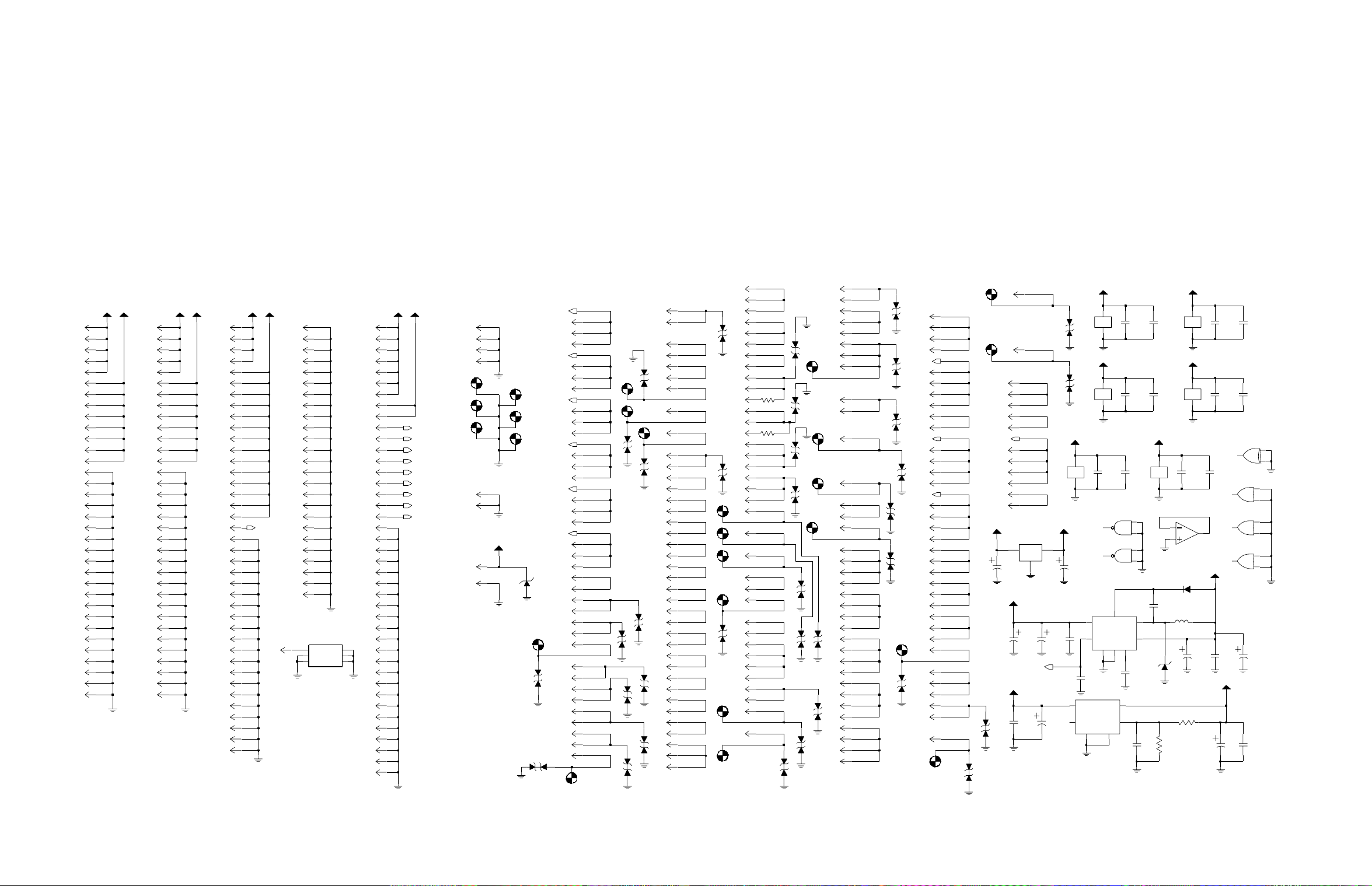
HDLCCLK
J2
43
J5
VR10
VR11
VR33
43
31
J7
HDLCDATA
J2
41
J5
41
29
J7
HST_REQ
J7
50
J9
67
LINE1+
J6
1
J21
1
R56
3
J22
LINE1-
J6
2
J21
2
R57
4
J22
LINE2+
J6
7
J22
1
J21
3
LINE2-
J6
8
2
J22
J21
4
M10
LINEPTTDTGCC
J8
16
M8
MONDET-GCC
J8
20
M23
MUTE-PLSTRIP
J8
62
ODC1
75
J2
J7
75
M11
M6
M25
J8
J7
J9
J2
J5
J7
J9
J8
J20
J8
J8
60
59
77
40
40
28
55
49
8
24
63
PTT
REFAUDIO
RESET
RINGINDICATOR
RSSI-GCC
RSTAT-PAHINH
VR15
0
0
VR21
VR22
VR23
VR24
VR32
VR31 VR30
VR14
M22
M3
M15
M4
VR34
SW+5
A+
22
J2
J2
23
J2
24
J2
25
J2
26
J2
27
J2
28
J2
29
30
J2
J2
31
J2
32
J2
33
J2
34
J2
1
J2
2
J2
3
4
J2
J2
18
J2
19
J2
20
J2
21
J2
35
J2
36
J2
59
61
J2
J2
63
J2
64
J2
67
J2
68
J2
71
J2
72
J2
73
J2
79
J2
80
22
J5
23
J5
24
J5
25
J5
26
J5
27
J5
28
J5
29
J5
30
J5
31
J5
32
J5
33
J5
34
J5
J5
1
J5
2
J5
3
4
J5
J5
18
J5
19
J5
20
J5
21
J5
35
J5
36
J5
57
59
J5
J5
63
J5
64
J5
67
J5
68
J5
71
J5
72
J5
73
79
J5
J5
80
SW+5
A+
5
J7
J7
6
J7
7
J7
8
J7
9
J7
10
J7
11
J7
12
13
J7
J7
14
J7
15
J7
16
J7
17
J7
18
J7
19
J7
20
21
J7
J7
22
J7
49
J7
1
J7
2
J7
3
J7
4
J7
23
24
J7
J7
51
J7
52
J7
53
J7
54
J7
57
J7
58
J7
61
62
J7
J7
65
J7
66
J7
72
J7
73
J7
79
J7
80
A+
PTT_REQ_SC
SW+5
J8
SW+5
A+
5
J8
J8
6
J8
13
J8
14
J8
26
J8
27
J8
28
J8
29
30
J8
J8
31
J8
38
J8
45
J8
46
J8
47
J8
48
J8
55
65
J8
J8
66
J8
70
J8
71
J8
72
J8
73
J8
75
J8
77
79
J8
U10
2
58
NC1
DATA
1
NC2
GND
3
NC3
NC
3
J9
J9
5
J9
6
J9
7
J9
8
J9
9
J9
10
J9
11
12
J9
J9
48
J9
49
J9
20
J9
19
J9
44
J9
46
J9
45
47
J9
J9
66
J9
1
J9
2
J9
13
J9
14
J9
23
J9
24
29
J9
J9
30
J9
39
J9
40
J9
41
4
J9
50
5
6
J9
51
J9
68
69
J9
J9
71
J9
72
J9
73
J9
74
J9
75
J9
76
J9
79
80
J9
AMUXCTRL
BMUXCTRL
PATEMP
VFINALFORWARD
X2MUX
X3MUX
Y2MUX
Y3MUX
PTT_REQ_EX
38
J6
J6
53
J6
79
J6
80
M9
M17
M19
J20
9
5
J21
J22
6
J22
8
M16
M18
M20
LN+5
VR25
VR6
M14
VR26
5.6V
A0-CS1
A1-CS2
J22
J21
J21
J21
J8
J2
J5
J7
J2
J5
J7
J2
J5
J7
J2
J5
J7
J2
J5
J7
J2
J5
J7
J2
J7
J8
J20
J8
J20
J8
J6
J6
J6
J6
53
53
41
54
54
42
A2
62
62
47
A3
60
60
46
A4
58
58
45
A5
56
56
44
74
74
57
56
61
48
39
35
52
64
7
2
7
8
7
6
M24
AGC1
ASYNC+
ASYNC-
AUXCARRIER
EXTPTT+
EXTPTT-
RDSTAT-
RDSTAT+
CCI-MONITOR
VR28
VR18
M2
M7
VR27
M1
VR29
VR8
VR9
VR17
VR19
VR20
CTS1
52
J8
J20
6
DATA*1
78
J2
J7
78
DATA1
J2
77
J7
77
DATAPTT-GCC
J8
21
DATARX-GCC
J8
22
DATATX-GCC
23
J8
DCD1
J8
54
J20
1
EXTSPARE#1
J2
5
5
J5
EXTSPARE#10
J2
14
J5
14
EXTSPARE#11
15
J2
J5
15
EXTSPARE#12
J2
16
J5
16
EXTSPARE#2
J2
6
6
J5
EXTSPARE#3
J2
7
J5
7
EXTSPARE#4
8
J2
J5
8
EXTSPARE#5
J2
9
J5
9
EXTSPARE#6
J2
10
10
J5
EXTSPARE#7
J2
11
J5
11
EXTSPARE#8
12
J2
J5
12
EXTSPARE#9
J2
13
J5
13
HDLCBUSY
J2
42
42
J5
J7
30
J8
J20
J2
J5
J7
J2
J5
J8
J8
J20
J8
J8
J2
J7
J8
J2
J5
J7
J9
J2
J5
J7
J9
J2
J5
J7
J9
J2
J5
J7
J9
J2
J5
J7
J9
53
4
65
65
55
17
17
68
50
3
19
25
76
76
17
47
47
35
56
48
48
36
57
49
49
37
58
50
50
38
60
51
51
39
61
RTS1
RX16.8MHZREF
RXAUDIO
RXD1
RXMUTE-GCC
RXPLDET
SBI1
SEIZERELSEGC
SPARE#1
SPARE#2
SPARE#3
SPARE#4
SPARE#5
VR37
VR40
VR38
VR39
M21
TXDATA-
J8
69
VR12
VR36
VR13
M12
J2
J5
J7
J9
SPICLK
J2
J5
J7
J9
J7
J9
SPIMISO
J2
J5
J7
J9
SPIMOSI
J2
J5
J7
J9
J2
J5
J7
J2
J5
J7
J2
J5
J7
J8
J5
J7
J9
J8
J20
J8
52
52
40
62
39
39
27
54
43
59
37
37
25
52
38
38
26
53
46
46
34
45
45
33
TDMFRAMESYNC
44
44
32
TSTAT-RXCAIE
59
TX16.8MHZREF
66
56
70
51
5
TXDATA+_TXAIO
67
M13
SPARE#6
SPIGRANT
TDMCLOCK
TDMDATA
TXD1
M5
TXPLINHITGCC
J8
15
TXWIDEBANDAIO
J2
69
J5
69
J7
63
VCOAUDIO
60
J7
J9
78
VCONTROL
J9
15
J9
16
J9
17
J9
18
XMITSPIREQ
J7
48
65
J9
A+ LN+5
MC78M05ACDT
1
C50
330UF 330UF
A+
C48
330UF
330UF
RESET_SWITCH
A+
C3
470pF
VR16
VR41
3
U14
2
C8
C9
470pF
C4
10uF
9.6V
4
GND
4
U3
U5
11
14
7
C73
0.1uF
8
MC74HC00
11
MC74HC00
6
BOOST
U6
TAB VC
8
OUT
ADJ
TAB
6
U16
U16
SENSE
1
470pF
VSW
1
2
C5
C26
0.1uF
C30
0.1uF
C74
470pF
C11
1500pF
POWER
VR42
VR43
POWER POWER
9.6V
4
POWER
U15
11
C51
5
IN
2
SHDN*
C77
100pF
5
IN
U7
4
SHDN*
GND
3
9
10
12
13
3
7
LN+5
POWER
U16
C27
470pF
C31
470pF
14
7
C10
0.27uF
R7
10.5K
1%
13
12
POWER
U15
MC33074
D1
L1
4.7UH
VR1
SCHOTTKY
MBRS330T3
R8
16.2K
1%
LN+5
14
C28
U4
0.1uF
7
LN+5LN+5
14
C32
0.1uF
U9
7
11
MC74HC86
C76
C75
470pF
0.1uF
6
MC74HC32A
SW+5
8
MC74HC32A
11
MC74HC32A
C13
470pF
9.6V
C6
10uF
14
C12
330UF 330UF
C29
470pF
C33
470pF
U5
12
13
U9
4
5
U9
9
10
U9
12
13
C49
C7
470pF
MAEPF-27077-O
Figure 18. PDR 3500 Schematic Sheet 2
11-4 January 31, 2001 68P81093C75-O
Page 79

Ω
Electrical Parts List : Backplane Circuit Board
Reference
C1 2113741B69 0.1uF
C2, C3 2113740F67 470
C4 2311049A19 10 uF
C5 2113740F67 470
C6 2311049A19 10uF
C7 2113740F67 470
C8 2313748R01 330uF
C9 2113740F67 470
C10 2113743B22 0.27uF
C11 2113741F29 1500
C12 2313748R01 330uF
C13 2113740F67 470
C14 2113741B69 0.1uF
C15 2113740F67 470
C16 thru C19 2113741F01 100
C21 2113741B69 0.1uF
C22 2113740F67 470
C23, C24 2113741F01 100
C26 2113741B69 0.1uF
C27 2113740F67 470
C28 2113741B69 0.1uF
C29 2113740F67 470
C30 2113741B69 0.1uF
C31 2113740F67 470
C32 2113741B69 0.1uF
C33 2113740F67 470
C34 2113741B69 0.1uF
C35 thru C37 2113740F67 470
C38 2113741B69 0.1uF
C39 2113740F67 470
C40, C41 2113741F01 100
C42 2113740F67 470
C43 2113741D28 0.22uF
C44, C45 2113740F67 470
C46 2113741B69 0.1uF
C47 2113740F67 470
C48 thru C51 2313748R01 330uF
C52 thru C54 2113740F31 15
C55 thru C59 2113740F41 39
Motorola Part
Number
Description
CAPACITOR, Fixed:
pF±5%; 50V Unless
otherwise stated
Electrical Parts List : Backplane Circuit Board
Reference
C60 2113741F01 100
C61, C62 2113740F67 470
C63 2113741F01 100
C64 2113741D28 0.22uF
C65 thru C72 2113741F01 100
C73 2113741B69 0.1uF
C74 2113740F67 470
C75 2113741B69 0.1uF
C76 2113740F67 470
C77 2113741F01 100
C80 2113741F01 100
C81 2113928E01 1uF
C82 2113741F01 100
D1 4805129M76 Silicon
D2 4813833A12 Silicon
J2 0982407W01 connector, 80-pin
J5 thru J9 0982407W01 connector, 80-pin
J20 2880007R05 connector, 10-pin
J21, J22 0960113B01 connector, RJ-45
L1 2485721C01 4.7uH
L2 thru L13 2462587T19 220nH
P1 thru P4 2985762C01 terminal, power
P5 2884324M08 header, 3-pin
P6, P7 2985762C01 terminal, power
P8 2884324M09 header, 4-pin
P9 2884324M10 header, 5-pin
P10 2885761C01 connector, 12-pin
Q1 thru Q4 4813821A47 mosfet
Q5 4813823A13 mosfet_gsd
Motorola Part
Number
Description
DIODE: See Note.
JACK:
COIL, RF: unless
otherwise stated
PLUG:
TRANSISTOR: See
Note.
Electrical Parts List : Backplane Circuit Board
Reference
R1 0662057P22 22.1k; 1%
R2 0662057P10 10k; 1%
R3 0662057P66 5.62k; 1%
R4 0662057P22 22.1k; 1%
R5 0662057Z35 11.5k; 1%
R6 0662057A49 1k
R7 0662057P12 10.5k; 1%
R8 0662057P16 16.2k; 1%
R9 0662057A73 10K
R10 0662057P66 5.62k; 1%
R11 0662057Y16 32.4k; 1%
R12 0662057P16 16.2k; 1%
R13 0662057P66 5.62k; 1%
R14 0662057A25 100
R16 0662057A39 390
R17, R18 0662057P20 20k; 1%
R19 0662057P18 18.2k; 1%
R20 0662057P10 10k; 1%
R21 0662057P16 16.2k; 1%
R22 0662057P12 10.5k; 1%
R24 0662057T73 33.2k; 1%
R25 thru R27 0662057B47 0
R28 0662057A49 1k
R31 0662057A73 10k
R32 0662057P66 5.62k; 1%
R33 0662057Z26 22.6k; 1%
R34 thru R36 0662057P10 10k; 1%
R37 0662057P12 10.5k; 1%
R38 0662057P10 10k; 1%
R39 0662057P18 18.2k; 1%
R40 0662057P16 16.2k; 1%
R41 0662057P12 10.5k; 1%
R42 thru R44 0662057A80 20k
R45 0662057A73 10K
R46 thru R48 0662057P10 10k; 1%
R49 0662057P12 10.5k; 1%
R50 0662057A77 15k
R51 0662057A73 10k
R52 0662057A68 6.2k
Motorola Part
Number
Description
RESISTOR, Fixed:
±5%; 1/8W unless
otherwise stated
Electrical Parts List : Backplane Circuit Board
Reference
R54
R55 0662057A80 20k
R56, R57 0662057B47 0
R59 0662057A25 100
R60 0662057A73 10k
R61 0662057A63 3.9k
R62 0662057A73 10k
S1 4080564C02 dip
U1, U2
U3 5113819A05 Op-amp, quad
U4 5113805A13 OR gate, quad
U5 5113805A22 XOR gate, quad
U6 5185130C93 Regulator, switching
U7 5105109Z13 Regulator, linear
U8 5185368C03 A/D converter
U9 5113805A13 OR gate, quad
U10 5185130C99 Silicon serial
U11 thru U13 5113805A84 multiplexer
U14 5113816A53 Regulator, 5V
U15 5113819A05 Op-amp, quad
U16 5113805A27 NAND Schmitt trigger
VR1 4813833B02 Zener
VR2 4813830A73 Zener, 2.8V
VR5 4813830A73 Zener, 2.8V
VR6 4813830A15 Zener, 5.6V
VR8 thru VR43 4813830A71 Zener, 15V
NOTE:
For optimum performance, order replacement diodes,
transistors, and cir cuit modules by Motorola part number only.
Motorola Part
Number
0662057A73 10k
5113805A84 multiplexer
Description
SWITCH:
MODULE:
number
DIODE: See Note.
68P81093C75-O January 31, 2001 11-5
Page 80
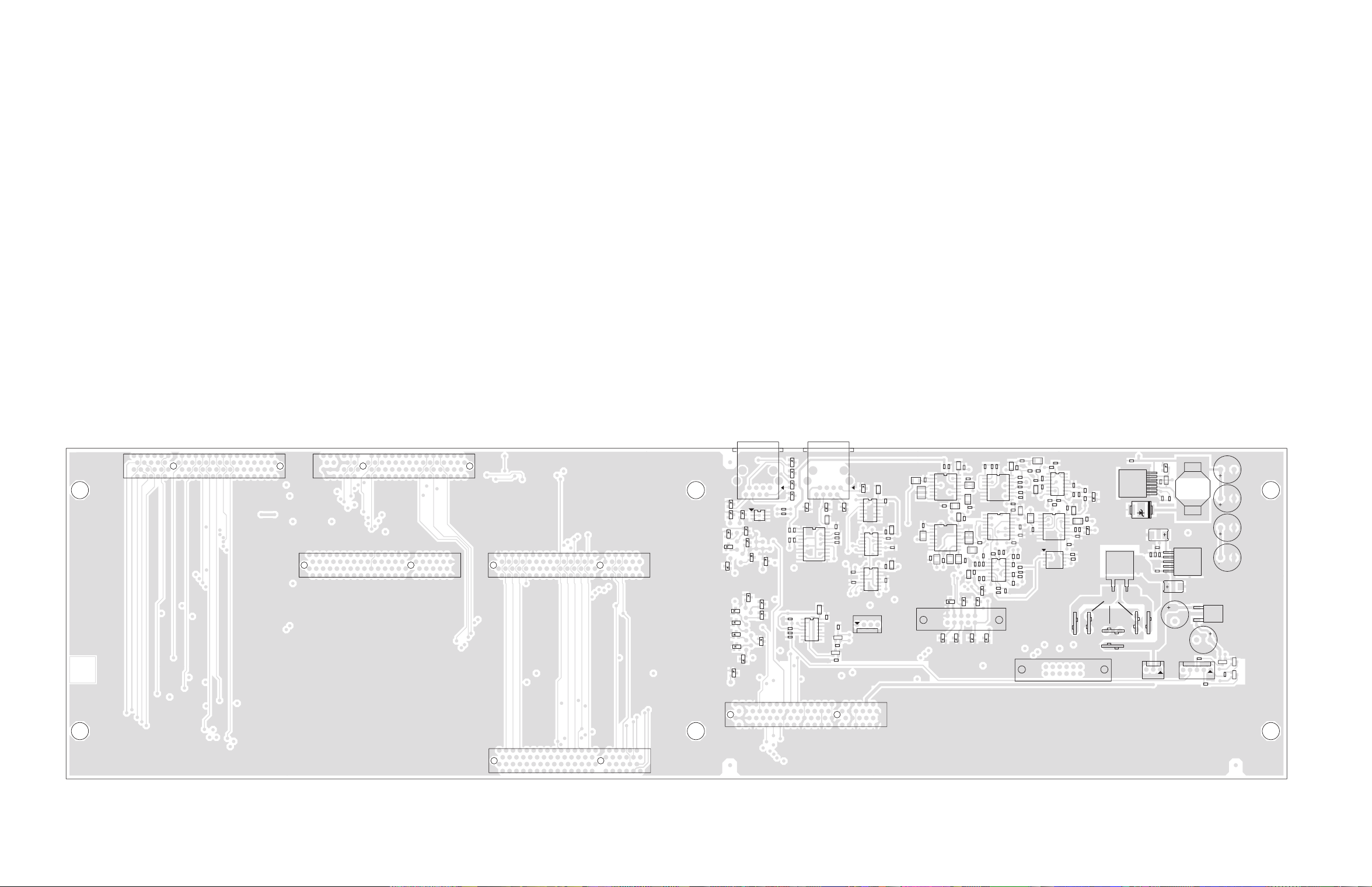
1
VIEWED FROM SIDE 1
80
78
79
77
56
58
J7
55
57
4
2
3
1
80
78
79
77
1
3
2
4
56
58
J8
55
57
57
J6
55
58
56
4
2
3
1
77
79
78
80
1
3
2
4
1
3
2
4
57
55
J5
58
56
57
55
J2
58
56
77
79
78
80
77
79
78
80
VR38
VR18
VR25
M24
VR26
M22
VR29
M1
M14
M13
VR40
VR30
VR34
VR39
VR36
J21
U10
VR37
M3
M9
VR41
M19
M20
VR42
M17
M15
M18
M21
VR32
M23
VR15
M25
VR43
M5
M7
M11
M12
M10
M8
M6
M4
M2
VR27
80
78
79
77
M16
VR28
VR33
VR31
VR21
VR19VR20
R56
R57
R1
R3
C80
R54
C81
J9
J22
VR22
VR6
VR17
C1
C2
20
1
R2
R4
U8
11
10
C75
C76
1
14
R60
U16
R55
D
7
8
G
S
D
S
G
R61
24
26
23
25
C32
VR23
1
14
C33
U9
VR24
7
8
C29
C52
C53
C54
C55
C56
Q4
R62
Q5
C28
1
14
C58
U4
C57
7
8
C31
C30
1
14
U5
C59
7
8
P8
4
2
3
1
R12
R13
C14
C15
C17
1
L7
16
C16
C43
C23
L5
C24
J20
L6
U2
9
8
L8
C18
L9
C19
C21
C22
161
U1
C63
C64
9
8
L3
C65
L4
VR14
R40
L11
L12
R41
C66
C27
C26
R46
VR8
VR11
VR16
1
9
2
10
VR9
VR10
R39
VR13
R26
1
8
8
R38
C69
R47
VR12
C60
R45
R27
R28
U11
U13
1
U3
7
C72
R48
L2
R50
R52
C34
16
9
C36
C47
161
C44
9
C61
R36
R37
R34
14
C70
C71
8
R49
R44
C35
1
14
R51
R24
C67
R11
U15
R10
R25
C37
C46
L10
C62
R35
R21
R22
R19
R31
R17
C74
78
R5
C73
C41
U12
C40
8
S1
BLU
2
1
C68
R18
R6
R16
C39
C38
161
L13
C82
R32
R33
9
C45
C42
R42
R43
P4
P3
RED
12
P10
11
C13
7
D1
U6
VR2
VR5
VR1
D2
BLK
P2
P7
P6
C10
C9
1
C77
C11
C6
C7
1
R7
P1
WHT
P5
U7
R8
C5
C3
5
C4
C50
C12
L1
C49
C8
C48
U14
C51
Q1
Q2
G
S
R14
G
D
S
D
P9
G
D
R9
S
Q3
R59
MAEPF-27078-O
Figure 19. PDR 3500 Backplane Circuit Board Detail
11-6 January 31, 2001 68P81093C75-O
Page 81

Mechanical Parts List: PLN1681A Main Chassis
Part Number Description Qty Where Used
0200001355
0200835638 Nut, elastic 4-40 4 AC receptacle and DC connector
0200844628 Nut, elastic 6-32 8 Fans
0300139392 Screw, 1/4-20 4 Handle
0300139800 Screw, 6-32 x .5 4 Preselector
0307644M09 Screw 10-32 x .75 8 Chassis to case
0307644M12 Screw 10-32 x .375 20 PA, backplane board, receiver and exciter brackets
0307644M28 Screw 4-40 x .437 6 RSS connector, DC connector, AC receptacle
0310907C83 Screw., M3 x .05 x 8 2 Receiver bracket.
0311995A17 Screw, 6-32 x 1 8 Fans
0385865C01 Screw, 8-32 x .250 4 Power supply
0385865C02 Screw, 8-32 x .312 8 Duplexer and duplexer cover
0400002645 Washer, lock #6 ext. 4 Preselector
0400002646 Washer, lock #8 int 2 Ground stud
0400007652 Washer, lock #10 ext 6 Backplane board
0400119331 Washer, split lock 4 Handle
0400490775 Washer, flat #6 2 Preselector
0407643M01 Washer, flat #10 8 Chassis to case
0485061D01 Spacer 2 Spacer for panel RF connectors
0705723V01 Clip, PA 1
0785688C01 Bracket, receiver 1
0785689C01 Bracket, exciter 1
1505432W01 Cover, PA 1
1585693C01 Cover, duplexer 1
2785687C01 Chassis 1
2800048250 Adapter, right angle UHF 2 On TX and RX port
2885828C01 AC Receptacle w/ fuse holder 1
3082933N02 Line cord 1
3085697C01 Coax cable, Exciter to PA 1
3085698C01 Cable, ribbon RSS 1
3085699C01 Cable, ribbon PA 1
3085700C01 Cable, PA power 1 PA to backplane board
3085701C01 Cable, DC power 1
3085702C01 Coax cable, PA to top panel 1
3085702C02 Coax cable, receiver to top panel 1
3085703C01 Wire, brown 1 Power supply to AC receptacle
3085703C02 Wire, orange 1 Power supply to AC receptacle
3085703C03 Wire, green/yellow 1 Chassis to AC inlet
3085703C04 Wire, black 1 Power supply to backplane board
3085703C05 Wire, white 1 Power supply to backplane board
3085703C06 Wire, green/yellow 1 Chassis to power supply
3085786C01 Coax cable, Duplexer to RX port 1
3085786C02 Coax cable, Duplexer to TX port 1
4085732C01 Assembly, PTT/LED 1
4385800C01 Standoff, hex 2 Preselector
4685799C01 Card guides 2
5507519M04 Handles 2
5882273C01 Adapter, N antenna 1 On duplexer
5985731C01 Fan assembly 2
6500139837 Fuse, 3A 250V 2
7505658W01 Thermal pad, PA 1
7582200H01 Pad, gray 6
7582200H14 Pad, black 8
7585798C01 Feet, rubber 4
Nut, 8-32 hex 2 Chassis ground stud
68P81093C75-O January 31, 2001 11-7
Page 82

Page 83

*6881093C75*
68P81093C75-O
4
Motorola
8000 West Sunrise Boulevard
Fort Lauderdale, Florida 33322
 Loading...