

T
查询PC33999EK供应商
Freescale Semiconductor, Inc.
MOTOROLA
SEMICONDUCTOR TECHNICAL DATA
Preliminary Information
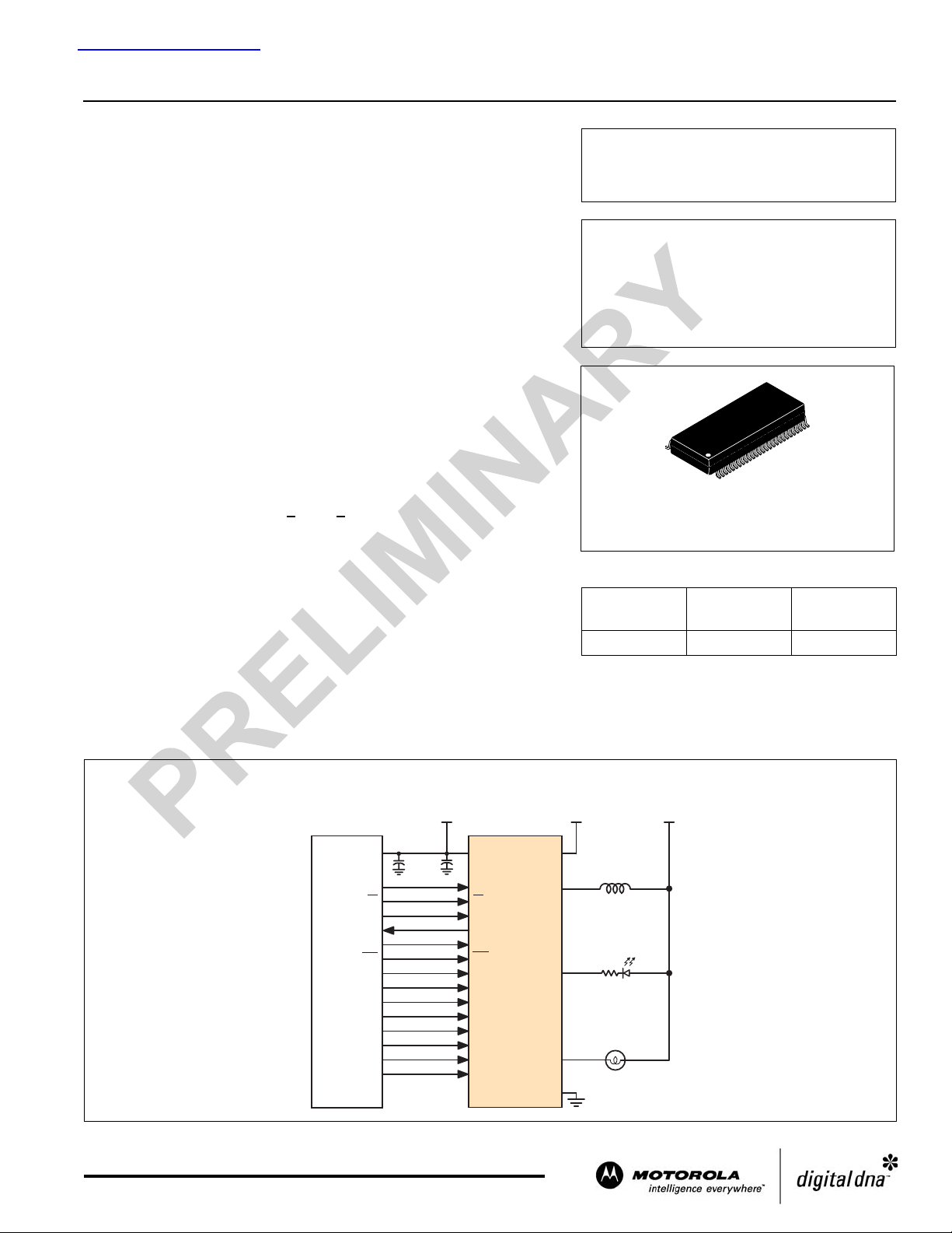
16-Output Switch with SPI and PWM
Control
The 33999 is a 16-output low-side switch with a 24-bit serial input control.
It is designed for a variety of applications including inductive, incandescent,
and LED loads. The Serial Peripheral Interface (SPI) provides both input
control and diagnostic readout. Eight parallel inputs are also provided for direct
Pulse Width Modulation (PWM) control of eight dedicated outputs.
Additionally, an output-programmable PWM input provides PWM of any
combination of outputs. A dedicated reset input provides the ability to clear all
internal registers and turn all outputs off.
The 33999 directly interfaces with microcontrollers and is compatible with
both 3.3 V and 5.0 V CMOS logic levels. The 33999, in effect, serves as a bus
nc...
I
expander and buffer with fault management features that reduces the MCU’s
fault management burden.
Features
• Designed to Operate 5.0 V <
• 24-Bit SPI for Control and Fault reporting, 3.3 V/5.0 V Compatible
• Outputs Are Current Limited (0.9 A to 2.5 A) to Drive Incandescent
Lamps
• Output Voltage Clamp of +50 V During Inductive Switching
• On/Off Control of Open Load Detect Current (LED Application)
•V
•R
• Independent Overtemperature Protection
• Output Selectable for PWM Control
• Output ON Short-to-V
• 54-Pin Exposed Pad Package for Thermal Performance
• Pb-Free Packaging Designated by Suffix Code EK
Standby Current < 10 µA
PWR
of 0.55 Ω at 25°C Typical
DS(ON)
cale Semiconductor,
V
< 27 V
PWR
and OFF Short-to-Ground/Open Detection
BAT
33999 Simplified Application Diagram
Simplified Application Diagram
33999 Simplified Application Diagram
3.3 V/5.0 V
33999
Document order number: MC33999
Rev 1.0, 01/2004
33999
POWER DUAL OCTAL SERIAL
SWITCH WITH SERIAL
PERIPHERAL INTERFACE I/O
EK (Pb-FREE) SUFFIX
54-LEAD SOICW EXPOSED PAD
Device
PC33999EK/R2 -40°C to 125°C 54 SOICW-EP
V
PWR
CASE 1390-01
ORDERING INFORMATION
Temperature
Range (T
V
BA
)
A
Package
Frees
This document contains information on a product under development.
Motorola reserves the right to change or discontinue this product without notice.
© Motorola, Inc. 2004
VDD VPWR
MCU
For More Information On This Product,
Go to: www.freescale.com
SOPWR
SCLKSCLK
CSCS
SIMISO
SOMOSI
PWMPWM
RSTRST
PWM0
PWM1
PWM6
PWM7
PWM8
PWM9
PWM14
PWM15
OUT0
OUT1
OUT2
OUT3
OUT4
OUT5
OUT6
OUT7
OUT8
OUT9
OUT10
OUT11
OUT12
OUT13
OUT14
OUT15
GND
Solenoid/Relay
LED
Lamp

Freescale Semiconductor, Inc.
V
PWR
8
nc...
I
cale Semiconductor,
Frees
PWM
50
RST
47
CS
23
SCLK
20
32
SO
35
SO
PWR
PWM0
PWM1
PWM6
24
PWM7
27
PWM8
28
PWM9
31
PWM14
51
PWM15
54
V
DD
10 µA
25 µA
10 µA
Input
Buffers
10 µA
SI
10 µA
Serial D/O
Line Driver
5
1
4
10 µA
10 µA
10 µA
10 µA
10 µA
10 µA
10 µA
10 µA
Overvoltage
Detect
OVD
V
RB
SFPDB
SFL
SCLK
CSB
SI
SO
CSI
CSBI
PWM0
PWM1
PWM6
PWM7
PWM8
PWM9
PWM14
PWM15
DD
Interface
Logic
Open
Detect
Enable
SPI
Load
Voltage
Regulator
GE
OT
SF
OF
V
DD
Bias
Gate
Control
V
Ref
50 µA
Short and
Open
Circuit
Detect
Overtemperature
Detect
From Detectors 1 to 15
50 V
I
To Gates
1to15
LIMIT
R
S
OUT0
2
OUT1–OUT 15:
3, 6, 7, 21, 22,
25, 26, 29, 30,
33, 34, 48, 49,
52, 53
GND Pins:
10–18
37– 40
42– 45
Figure 1. 33999 Simplified Internal Block Diagram
33999 MOTOROLA ANALOG INTEGRATED CIRCUIT DEVICE DATA
2
For More Information On This Product,
Go to: www.freescale.com

Freescale Semiconductor, Inc.
nc...
I
cale Semiconductor,
Frees
PWM0
OUT0
OUT1
PWM1
SOPWR
OUT2
OUT3
VPWR
NC
GND
GND
GND
GND
GND
GND
GND
GND
GND
NC
SCLK
OUT4
OUT5
CS
PWM6
OUT6
OUT7
PWM7
1
2
3
4
5
6
7
8
9
10
11
12
13
14
15
16
17
18
19
20
21
22
23
24
25
26
27
PWM15
54
OUT15
53
OUT14
52
PWM14
51
PWM
50
OUT13
49
OUT12
48
RST
47
NC
46
45
GND
44
GND
43
GND
42
GND
41
NC
40
GND
39
GND
38
GND
37
GND
36
NC
35
SO
34
OUT11
33
OUT10
32
SI
31
PWM9
30
OUT9
29
OUT8
28
PWM8
PIN FUNCTION DESCRIPTION
Pin Pin Name Formal Name Definition
1, 4,
24, 27, 28, 31,
51, 54
2, 3, 6, 7,
21, 22, 25, 26,
29, 30, 33, 34,
48, 49, 52, 53
5 SOPWR SO
8 VPWR Battery Input Battery supply input pin.
9, 19, 36, 41,
46
10–18,
37–40,
42–45
20 SCLK System Clock System Clock for internal shift registers of the 33999.
23 CS Chip Select SPI control chip select input pin from MCU to 33999.
32 SI Serial Input Serial data input pin to the 33999.
35 SO Serial Output Serial data output pin
47 RST Reset Active low reset input pin.
50 PWM PWM Control Pin PWM control input pin. Supports PWM on any combination of outputs.
PWM0, PWM1,
PWM6–PWM9,
PWM14, PWM15
OUT0–OUT15 Output 0– Output 15 Low-side driver outputs.
NC No Connect These pins have no connection.
GND Ground Ground for logic, analog, and power output devices.
PWMn Input Parallel PWM control Input pins. Allows direct PWM control of eight outputs.
Supply Pin Power supply pin to the SO output driver.
PWR
MOTOROLA ANALOG INTEGRATED CIRCUIT DEVICE DATA 33999
For More Information On This Product,
Go to: www.freescale.com
3
Freescale Semiconductor, Inc.
MAXIMUM RATINGS
All voltages are with respect to ground unless otherwise noted.
Rating Symbol Value Unit
VPWR Supply Voltage (Note 1) V
SPI Interface Logic Supply Voltage (Note 1) SO
SPI Interface Logic Input Voltage (CS, PWM, SI, SO, SCLK, RST, PWMn)
(Note 1)
Output Drain Voltage
Frequency of SPI Operation (Note 2)
Output Clamp Energy (Note 3) E
ESD Voltage (Note 4)
Human Body Model (Note 5)
Machine Model (Note 6)
nc...
Storage Temperature T
I
Operating Case Temperature T
Operating Junction Temperature T
Power Dissipation (TA = 25°C) (Note 7) P
Lead Soldering Temperature (Note 8) T
Thermal Resistance
Junction-to-Ambient (Note 9)
Junction-to-Case (Note 10)
Junction-to-Board
Notes
1. Exceeding these limits may cause malfunction or permanent damage to the device.
2. This parameter is guaranteed by design but not production tested.
3. Maximum output clamp energy capability at 150°C junction temperature using single non-repetitive pulse method.
4. ESD data is available upon request.
5. ESD1 testing is performed in accordance with the Human Body Model (C
6. ESD2 testing is performed in accordance with the Machine Model (C
cale Semiconductor,
7. Maximum power dissipation with no heat sink used.
8. Lead soldering temperature limit is for 10 seconds maximum duration. Not designed of immersion soldering. Exceeding these limits may
cause malfunction or permanent damage to the device.
9. Tested per JEDEC test JESD52-2 (single-layer PWB).
10. Tested per JEDEC test JESD51-8 (two-layer PWB).
Frees
ZAP
= 200 pF, R
ZAP
PWR
PWR
V
IN
V
DS
f
SPI
CLAMP
V
ESD1
V
ESD2
STG
C
J
D
SOLDER
R
JA
θ
R
JC
θ
R
JB
θ
= 100 pF, R
ZAP
= 1500 Ω).
ZAP
= 0 Ω).
-1.5 to 50 V
-0.3 to 7.0 V
-0.3 to 7.0 V
-0.3 to 45 V
6.0 MHz
50 mJ
±2000
±200
-55 to 150 °C
-40 to 125 °C
-40 to 150 °C
2.0 W
260 °C
60
1.2
8.0
V
°C/W
33999 MOTOROLA ANALOG INTEGRATED CIRCUIT DEVICE DATA
4
For More Information On This Product,
Go to: www.freescale.com
Freescale Semiconductor, Inc.
STATIC ELECTRICAL CHARACTERISTICS
Characteristics noted under conditions of 3.1 V ≤ SO
noted. Where applicable, typical values reflect the parameter’s approximate average value with V
Characteristic Symbol Min Typ Max Unit
≤ 5.5 V, 5.0 V ≤ V
PWR
≤ 18 V, -40°C ≤ TC≤ 125°C, unless otherwise
PWR
=13V, TA=25°C.
PWR
POWER INPUT
Supply Voltage Range
Fully Operational
Supply Current
All Outputs ON, I
Sleep State Supply Current at
0.5 V
Overvoltage Shutdown V
Overvoltage Shutdown Hysteresis V
nc...
I
VPWR
Undervoltage Shutdown V
SPI Interface Logic Supply Voltage SO
SPI Interface Logic Supply Current (
SPI Interface Logic Supply Current (
SPI Interface Logic Supply Undervoltage Lockout Threshold SO
OUT
= 0.3 A
RST ≤ 0.2 SO
RST Pin High) I
RST Pin Low) I
and/ or SO
PWR
PWR
≤
V
PWR(FO)
I
PWR(ON)
I
PWR(SS)
OV
OV (
)
HYS
PWR(UV)
PWR
SOPWR(RSTH)
SOPWR(RSTL)
PWR(
UNVOL
5.0 – 27
–4.08.0
-10 1.0 10
27.5 31.5 35 V
0.8 1.4 2.3 V
–3.23.5V
3.1 – 5.5 V
100 – 500
-10 – 10
2.0 2.5 3.0 V
)
V
mA
µA
µA
µA
cale Semiconductor,
Frees
POWER OUTPUT
Drain-to-Source ON Resistance (I
= 125°C
T
J
T
= 25°C
J
T
= -40°C
J
Output Self-Limiting Current
Outputs Programmed ON
Output Fault Detect Threshold (Note 11)
Outputs Programmed OFF
Output OFF Open Load Detect Current (Note 12)
Outputs Programmed OFF (V
Outputs Programmed OFF (V
Output Clamp Voltage
2.0 mA ≤ I
Output Leakage Current
SO
PWR
Overtemperature Shutdown (Outputs OFF) (Note 13) T
Overtemperature Shutdown Hysteresis (Note 13) T
Notes
11. Output Fault Detect Thresholds with outputs programmed OFF. Output Fault Detect Thresholds are the same for output open and shorts.
12. Output OFF Open Load Detect Current is the current required to flow through the load for the purpose of detecting the existence of an open
load condition when the specific output is commanded to be OFF.
13. This parameter is guaranteed by design but is not production tested.
OUT
≤ 2.0 V
≤ 200 mA
= 0.35 A, V
OUT
= 5.0 V)
PWR
= 13 V, 18 V)
PWR
PWR
= 13 V)
R
DS(ON)
I
OUT(
lim
V
OUTth(F)
I
OCO(5)
I
OCO(13,18)
V
CL
I
OUT(
lkg
LIM
LIM(
hys
–
–
–
)
0.9 1.2 2.5
2.5 3.0 3.5
0.75
0.55
0.45
1.2
1.2
1.2
µA
25
30
45 50 55
)
-10 2.0 10
155 165 180 °C
)
5.0 10 20 °C
50
50
100
100
µA
Ω
A
V
V
MOTOROLA ANALOG INTEGRATED CIRCUIT DEVICE DATA 33999
For More Information On This Product,
Go to: www.freescale.com
5
 Loading...