

Page 1

INSTRUCTION MANUAL
ISOPROBE® ELECTROSTATIC VOLTMETER
MODEL 279L
110309
P/N 0340177
Accessories Included:
Manual
Line Cord
Probe Cover Plug
100 Housel Ave PO Box 535 Lyndonville NY 14098 1-800-821-6001 585-765-2254 fax: 585-765-9330 monroe-electronics.com
Page 2

PRODUCT WARRANTY
Monroe Electronics, Inc., warrants to the Owners, this instrument to be free from defects in material and
workmanship for a period of two years after shipment from the factory. This warranty is applicable to the original
purchaser only.
Liability under this warranty is limited to service, adjustment or replacement of defective parts (other than tubes,
fuses or batteries) on any instrument or sub-assembly returned to the factory for this purpose, transportation
prepaid.
This warranty does not apply to instruments or sub-assemblies subjected to abuse, abnormal operating conditions,
or unauthorized repair or modification.
Since Monroe Electronics, Inc. has no control over conditions of use, no warranty is made or implied as to the
suitability of our product for the customer’s intended use.
THIS WARRANTY SET FORTH IN THIS ARTICLE IS EXCLUSIVE AND IN LIEU OF ALL OTHER WARRANTIES
AND REPRESENTATIONS, EXPRESS, IMPLIED OR STATUTORY INCLUDING BUT NOT LIMITED TO THE
IMPLIED WARRANTIES OF MERCHANTABILITY AND FITNESS. Except for obligations expressly undertaken by
Monroe Electronics, in this Warranty, Owner hereby waives and releases all rights, claims and remedies with
respect to any and all guarantees, express, implied, or statutory (including without limitation, the implied warranties
of merchantability and fitness), and including but without being limited to any obligation of Monroe Electronics with
respect to incidental or consequential damages, or damages for loss of use. No agreement or understanding
varying or extending the warranty will be binding upon Monroe Electronics unless in writing signed by a duly
authorized representative of Monroe Electronics.
In the event of a breach of the foregoing warranty, the liability of Monroe Electronics shall be limited to repairing or
replacing the non-conforming goods and/or defective work, and in accordance with the foregoing, Monroe
Electronics shall not be liable for any other damages, either direct or consequential.
RETURN POLICIES AND PROCEDURES FACTORY REPAIR
Return authorization is required for factory repair work. Material being returned to the factory for repair must have a
Return Material Authorization number. To obtain an RMA number, call 585-765-2254 and ask for Customer
Service.
Material returned to the factory for warranty repair should be accompanied by a copy of a dated invoice or bill of
sale, which serves as a proof of purchase for the material. Serial numbers and date codes on our products also
serve to determine warranty status. Removal of these labels or tags may result in voiding a product’s warranty.
Repairs will be returned promptly. Repairs are normally returned to the customer by UPS within 10 to 15 working
days after receipt by Monroe Electronics, Inc. Return (to the customer) UPS charges will be paid by Monroe
Electronics on warranty work. Return (to the customer) UPS charges will be prepaid and added to invoice for outof-warranty repair work.
RETURN OF REPAIRED ITEMS:
Factory repairs will be returned to the customer by the customer’s choice of FedEx, DHL or UPS. Warranty repairs
will be returned via UPS ground. The customer may request accelerated shipping via the previous mentioned
carriers for both warranty and non-warranty repairs.
repairs will always be at the expense of the customer despite the warranty status of the equipment.
FACTORY REPAIRS TO MODIFIED EQUIPMENT:
Material returned to the factory for repair that has been modified will not be tested unless the nature and purpose of
the modification is understood by us and does not render the equipment untestable at our repair facility. We will
reserve the right to deny service to any modified equipment returned to the factory for repair regardless of the
warranty status of the equipment.
NOTE: Accelerated transportation expenses for all factory
website: www.monroe-electronics.com e-mail: electrostatics@monroe-electronics.com
Page 3

MODEL 279L
ISOPROBE® ELECTROSTATIC VOLTMETER
TABLE OF CONTENTS
I. SPECIFICATIONS ..........................................................................PAGE 1
II. INSTALLATION .............................................................................. PAGE 3
III. CONTROLS AND INDICATORS ....................................................PAGE 5
IV. OPERATION................................................................................... PAGE 7
V. THEORY .........................................................................................PAGE 8
VI. ADJUSTMENT..............................................................................PAGE 10
VII. TROUBLESHOOTING.................................................................. PAGE 14
APPENDIXES:
MODEL 1034 PROBE MOUNTING..... APPENDIX I……………………….Page 16
POWER ENTRY MODULE..... APPENDIX II………………………………..Page 18
HV BREAKDOWN CONSIDERATIONS.....APPENDIX III………………...Page 20
ACHIEVING SPACING INDEPENDENCE ....APPENDIX IV……………...Page 21
iii
Page 4

SECTION 1
SPECIFICATIONS
A. Applications:
Model 279L ISOPROBE®ELECTROSTATIC VOLTMETER takes advantage of Monroe’s years of experience in
design of reliable instruments for
modern semiconductor technology. A full spectrum of proven-design interchangeable probes exposes broad new
areas for exploratory research as well as providing a precision instrument for routine applications in electrostatic
measurements. Some typical and potential applications include:
Disk media research
IC manufacturing and handling
Materials evaluation
Contact potential measurements
Bioelectric field studies
Process monitoring and control
B. Features:
Low profile half rack size for multi-channel applications
NON-CONTACTING measurement of electrostatic potential combined with
Full complement of interchangeable probes
Analog recorder output
LED meter with “blackout switch” for darkroom applications
C. Range:
0 to ±300 volts DC
D. Accuracy:*
0.1% of full scale or 10mV, whichever is greater, 0.003%/C over +20 to +40C range (at recorder
output). Useable to +50
E. Meter resolution:
100mV (4 ½ digit LCD)
F. Speed of response:*
3ms, 10% to 90%, achievable at probe to surface spacing up to 0.1” with low resolution probe.
G. Settling time:
<6½ms to 1% of final value.
C.
H. Frequency response:
Small signal frequency response typically 3db to >300Hz.
Page 1
Page 5

I. Drift:*
<0.01V/hr after 1 hr stabilization (0.003V/hr typical). Not measurably affected by 10C temperature
variation or changes between 10% and 90% relative humidity.
J. Noise:*
<90mV rms referred to input, typical.
K. Surface resolution:
Determined by probe aperture size and surface-probe separation. Standard type 1034E & S probes
with 0.07” (1.75mm) aperture will resolve a 0.10” (2.5mm) spot at 0.02” (0.5mm) separation.
L. Recorder output:
100:1, 3 volts full-scale
M. Output filter:
Bessel low pass filter with 1.2ms constant delay.
N. Size:
1.7 x 8.2 x 15.1 inches (44 x 208 x 384mm), 1.75” rack mounting available (1 or 2 per rack).
Weight 4 lb. (1.8kg).
O. Power requirement:
100, 120, 230 or 240 VAC, 10%, 50/60Hz, 15 watts.
1
/4A SB for 100 & 120 V (Littelfuse 313.250 or equiv.)
Fuse
1
/8A 5x2mm for 230 & 240 V (Littelfuse 217.125 or equiv.)
Fuse
* Dependent on specific probe model, probe-to-surface separation and environment. Specifications shown are for
standard Type 1034E or S probes in a normal laboratory atmosphere. Separation for accuracy and response speed
tests is
environments and may be degraded under exceptionally dirty or dusty conditions or in ambiance of unstable
gaseous constituents.
1
/8” (3mm) and for noise and drift tests, 0.005” (0.13mm). Performance generally improves in controlled
PROBES:
Monroe Electronics Type 1034E (end viewing) or 1034S (side-viewing) probes are 0.35” (9mm) x 0.35” (9mm) x
3.25” (82.6mm) in length. Add 0.8” (20mm) length for cable at minimum bend radius. Contains 1kHz tuning fork
chopping driver and onboard hybrid microcircuit preamp. Useable from -50
configurations are available for high or low resolution and transparent probes for light decay measurements. Length
of probe cable is 10 ft. (3.05 meters). Provision has been made for air or inert gas purging of probe. Standard basic
instrument package includes Model 279L electrostatic voltmeter, line cord and instruction manual. Rear mounted
connector on instrument is standard; front panel connector is optional. Unit is calibrated independent of probe and
includes certificate of NIST traceability. Interchangeable Model 1034 probe (type specified by customer) is sold
separately.
C to +80C. Optional probe
Page 2
Page 6

SECTION 2
INSTALLATION
CAUTION:
Before plugging instrument in, make certain that it is matched to local power line voltage. The factory set line
voltage may be determined by the position of the voltage selector indicator pin in the power entry module. All units
are shipped configured for 120 VAC unless otherwise specified. In the event that it is necessary to change the
operating voltage of the instrument (or inspect or replace the fuses), see Appendix II for more information.
NOTE:
Wire Color Code for Line Cord Provided.
HIGH SIDE OF LINE - BLACK or BROWN
LOW SIDE OF LINE - WHITE or LIGHT BLUE
SAFETY GROUND - GREEN or GREEN/YELLOW
A. Probe mounting:
The 1034 and all other compatible probes must be mounted with the sensitive aperture facing the surface to be
measured.
The probe must be electrically isolated for up to about 400V, since the probe acquires the potential of the surface
being measured.
Further probe mounting information is given in Appendix I.
B. Probe-to-surface spacing:
CAUTION:
When operating at very close probe-to-surface spacing -- BEWARE OF PROBE-TO-SURFACE ARC-OVER and
possible accidental physical contact. Refer to Appendix III for further information.
Probe to surface spacing should be maintained as close as physically reasonable for best performance. Typical
spacing range is from .005” (0.1mm) for unknown voltages below 500 volts to over .125” (3mm) for unknown
voltages up to 3000 volts.
As probe to surface spacing increases instrument performance will suffer:
1. Decreased Accuracy
2. Decreased Speed-of-Response
3. Decreased Surface Resolution
4. Increased Noise
5. Increased Drift
C. System grounding:
The instrument is normally grounded via power cord and the potential measured is referenced to ground. A rear
panel ground connection is provided.
D. Output circuitry:
The output connector is a BNC connector mounted to the rear panel. The output voltage unless otherwise specified
is the measured voltage divided by 100. Normal useable output range is ±3V.
Page 3
Page 7

E. Probe purging:
Probe purging improves instrument performance especially with regard to zero stability, noise and sensitivity to
variations in probe-to-surface spacing. An optional purge kit Model 1017/22G available from Monroe Electronics
maintains an even airflow, reduces temperature variations and filters out dust and other particles.
Contact potential is a function of these variables and should be considered when making any changes in the purging
techniques. Care should be taken to maintain the purged air as free from chemical vapor contamination as
possible.
Probes may also be purged using clean, dry oil-free air from a local source or through the use of dry nitrogen or
other inert gas. Pressure needs only be sufficient to maintain a positive flow of gas out of the sensitive aperture to
prevent foreign materials from entering and, in no case should it exceed ½ psi (14” w.c.). All materials used should
have low out-gassing properties.
For best results, leave purge in continuous operation. For long term storage, cover the end of the probe with the
plastic cap supplied or with aluminum foil to seal against contamination.
Page 4
Page 8

SECTION 3
CONTROLS AND INDICATORS
FRONT PANEL - Figure 3-1
A. STBY/OPER Switch:
This push-push switch controls the operating condition of the unit. So long as power is applied, the following is true:
STANDBY Starts the probe oscillating but leaves the high voltage disabled.
OPERATE Activates high voltage only if the probe is plugged in and the tuning fork is oscillating.
B. Display:
The 4½-digit LED display is normally illuminated when power is applied to the unit and acts in a secondary capacity
as a power indicator.
A minus (-) sign at the left side of the display indicates that a negative voltage is being measured and is displayed
approximately 50% of the time (a polarity indecision) when the instrument is properly zeroed while measuring an
input signal of zero. No sign is displayed for a positive input.
The display may be turned off for darkroom use by actuating the push-push display switch through the access hole
in the panel with a suitable tool such as the point of a pen.
C. ZERO 1:
Balances internal probe contact potential to obtain probe to surface spacing insensitivity. This adjustment
procedure is described in Section 4A. ZERO 1 may also be used for large zero offset when spacing insensitivity is
not needed.
D. GAIN:
Closed loop system gain varies with probe to surface spacing. Excessive gain at close spacing causes instability
and insufficient gain at large spacing produces sluggish response and static error.
E. ZERO 2:
Compensates for unwanted system offsets over a range of approximately ±4 volts and does not affect probe to
surface spacing insensitivity. Adjustment procedure is outlined in Section 4. Once set, this operator accessible
adjustment usually does not require further attention except in critical applications.
F. Probe receptacle:
Mates with Model 1034 series probes manufactured by Monroe Electronics. An appropriate and functional probe
must be connected for the instrument to operate.
To connect the probe to the instrument, hold the plug (on probe cable) so that the two arrows are on top. Align with
the receptacle and push straight in until a “click” is heard.
To disconnect, hold the part with the two arrows and pull straight out. This will release the locking device.
Do not connect or disconnect the probe with power applied.
Page 5
Page 9

REAR PANEL - Figure 3-2
G. Power Entry Module:
The Power Entry Module combines power inlet, switch and fusing system. Power supply voltage is usually factory
preset for local conditions.
When in doubt, check! See Appendix II for details.
H. Ground jack:
Instrument ground - the reference point for measurement. The instrument is normally grounded through the power
cord. This jack accepts a standard size banana plug (0.175” [4.4mm] across flats).
I. Recorder output:
The signal at this BNC jack is a low voltage representation of the input. The output voltage is equal to the measured
voltage measured divided by 1000 or 0 to ±3 volts for full scale (±17 volts full scale typical for ÷200 option and ±19
volts full scale typical for ÷100 option). Representative uses include observation or recording of waveforms or levels
seen by the input, monitoring of safe/unsafe electrostatic operating conditions in equipment and low level process
control in electrostatic feedback loops.
J. Probe receptacle:
Duplicate of (F) provides the option of a probe connection at the rear of the instrument. Only one or the other may
be used. Model 279 will not support two probes simultaneously.
Page 6
Page 10

SECTION 4
OPERATION
CAUTION:
Verify that instrument operating voltage matches local power line voltage. See Section 2 and Appendix II.
PRECAUTIONARY NOTE
Model 279 is a non-contacting voltmeter. The potential of the probe will attempt to follow the potential of any object
within the field of view of the sensitive electrode (up to
of operator safety and also to reduce high voltage stress within the instrument, it should be left in the STANDBY
mode whenever it is not being used and particularly when the probe will not be “looking” at a surface potential of
less than 3000V.
A. Initial setup:
As shipped from the factory, the instrument is set up to make general-purpose electrostatic measurements except
for zero adjustment.
1. Position probe approximately
2. Switch into OPERATE mode.
3. Adjust ZERO 1 for an indication of 0000 on meter.
1
/8” from a grounded surface.
3400 volts) when the instrument is operating. In the interest
4. Proceed with measurements.
B. Restoration of factory settings:
The following steps are necessary only if the factory settings of ZERO 2 and/or GAIN controls have been disturbed
as evidenced by a constant zero offset or unstable performance at close probe to surface spacing.
ZERO 2
1. With the probe positioned as above, switch into STANDBY mode.
2. Adjust ZERO 2 for an indication of 0000 with approximately 50% polarity indecision.
GAIN
This adjustment requires a metallic test surface at least 3- 4 inches (50-75mm) square and a means of applying
repetitive pulses or square waves to it. Amplitude should be in the order of 100-300 volts with a rise time
significantly better than 2 milliseconds. An oscilloscope is also required.
1. Set GAIN to maximum counterclockwise (CCW ) rotation.
2. Position probe 0.005” (0.13mm) from the test surface.
3. Apply repetitive pulses to the test surface while observing the output of the 279.
4. Adjust GAIN for optimized transient response (fastest rise time with minimum overshoot and no oscillatory
tendency).
Page 7
Page 11

SECTION 5
THEORY
A. General: Principle of Operation (See Figure 5-1)
The electrostatic electrode "looks" at the surface under measurement through a small hole at the base of the probe
assembly. The chopped AC signal induced on this electrode is proportional to the differential voltage between the
surface under measurement and the probe assembly. Its phase is dictated by the DC polarity.
The reference voltage and this mechanically modulated signal, conditioned by the high input impedance preamplifier
and signal amplifier are fed to a phase sensitive detector whose output DC magnitude and polarity are dictated by
the amplitude and phase of the electrostatically induced signal relative to the reference signal. The output of the
phase sensitive detector feeds a DC integrating amplifier. Its output polarity is inverted to that of the unknown. The
output of this amplifier is used to drive a high voltage amplifier, which in turn drives the probe to the same potential
as that of the surface under measurement.
The probe is driven to a DC voltage typically within 0.1% of the potential of the unknown for a 2-3mm probe-tosurface spacing. By simply metering the output of the H.V. amplifier, one has an accurate indication of the unknown
potential.
Figure 5-1
B. Null balance: (ZERO 1)
This instrument's basic operating principle, i.e., "field-nulling" provides a high degree of immunity to errors in
measurement caused by variations in probe-to-surface separation. As long as the probe and the surface under
measurement are at the same potential the electrical field between them is zero, neglecting fringing, regardless of
the probe-to-surface distance.
Page 8
Page 12

If, however there exist voltage sources in the vicinity of the sensitive electrode which are independent of the
unknown to be measured, the offsets produced will detrimentally affect the spacing independence. Such voltage
sources include contact potential differences among the internal probes parts, small specks of charged dust
particles, etc.
The null balance circuitry is provided to neutralize such offsets by applying a voltage directly to the sensitive
electrode.
C. Zero: (ZERO 2)
The instrument's zero control is a voltage source connected in the metering circuitry. It is used to overcome offsets
produced by voltage sources external to the probe.
D. Gain:
The instrument functions as a closed loop unity gain voltage follower. Its open loop gain from probe to integrator is
determined by the gain of various amplifiers. The exact gain required for optimum transient responses during a
specific measurement is determined by the probe-to-surface spacing used. In order to accommodate
measurements at various probe-to-surface separations, a front panel gain control is provided which controls the
gain of the signal amplifier.
Page 9
Page 13

SECTION 6
ADJUSTMENT
A. General:
The following procedure sequence is such that it will aid in troubleshooting the unit. The circuit board layout is
illustrated in 3570/22. All test points and reference numbers used in this section are indicated on schematic 279L/1,
assembly drawing 3570/22 and are identified in Table 6-2 at the end of this section.
The procedure should be followed in the order given to prevent possible interaction of controls.
A phase-compensated (normal) Monroe Electronics, Inc. Model 1034E or 1034S miniature probe must be used
wherever the use of a probe is indicated.
B. Recommended Equipment:
Oscilloscope – 50kHz bandwidth, 0.1mV/div sensitivity
Compensated high voltage probe for oscilloscope (optional)
High voltage source –
Digital voltmeter – five-digit, 0.1mV resolution
High voltage probe – 1000:1,
Shorting plug, ME P/N 9232301, Keystone P/N 1463 (used at JP8)
500V, Stanford Research Systems Model PS350 or equivalent
0.01% (for DVM)
C. Initial Setup and Adjustments:
1. Insure that available nominal power line voltage and frequency match those shown of the back panel of the
unit and that the line voltage selector is properly configured. (See Section 2, INSTALLATION).
apply power at this time.
2. Remove cover from unit.
3. Consult Table 6-2. Make the following potentiometer adjustments: Set R53, R54, R108 and R111 to
midrange. Set R55 and R56 counterclockwise. Set R107 clockwise.
4. Connect a probe to the rear panel connector and fixture it to look at a metal test plate at least six inches
(150mm) square at a distance of 0.005 inch (0,13mm).
5. Connect a high voltage source to the test plate and set its output for zero volts.
6. Install a shorting plug at JP8 and disconnect P300. Jumpers JP1, JP3, JP4, JP6, and JP7 should be
installed.
7. On the front panel, put the OPER/STBY switch in STBY and turn on the display.
Do not
8. Connect the 279 to the appropriate source of power and turn on the rear panel power switch.
D. Low Voltage Power Supply Check:
Check the following test points with a digital voltmeter between the test point and chassis.
Test Point D.V.M. Reading
TP15
TP16
TP18
TP20
-15 VDC 0.5 V
+15 VDC 0.5 V
+15 VDC 0.5 V
-15 VDC 0.5 V
Table 6-1
Page 10
Page 14

E. Probe Oscillator Adjustment:
Connect an oscilloscope probe to TP5 and adjust R53 for a 6 Vp-p sine wave.
F. Demodulator Phase Adjustment:
1. Move the oscilloscope probe to TP3 and adjust the ZERO 1 pot on the front panel for a null (straight line) on
the oscilloscope.
2. Apply +10V to the test plate and adjust R65 for the best representation of a negative going half-wave
rectified sine wave with an amplitude of about 0.2V.
3. Switch the test plate voltage to –10V and the oscilloscope should display a positive going half wave.
G. FET String Bias Adjustment:
1. Switch off the rear panel power switch.
2. Remove JP4.
3. Tie TP8 to TP6.
4. Connect a DVM acrossR309 of the 279L/71 board.
5. Connect P300.
rectifier.
6. Switch on the rear panel power switch.
7. Adjust R55 for 40mV on the DVM.
8. Move the DVM from R309 to R311.
9. Adjust R56 to match the N-FET bias reading. Switch off the rear panel power switch.
WARNING! When the power is on, high voltage will be present on the high voltage
H. High Voltage Adjustment:
1. Remove the ground from TP8.
2. Remove the jumper at JP8.
3. Replace jumper JP4.
4. Connect the DVM from chassis ground to end of R303 nearest the edge of the 279L/71 board and the DVM
should read about +390V.
5. Move the DVM input lead to the end of R314 nearest the edge of the 279L/71 board and DVM should read
about -390V.
6. Remove the DVM.
I. Speed of Response:
1. Set the gain pot, front panel recessed, for about midrange.
2. Connect the oscilloscope to the rear panel output connector.
3. With the 279L in standby, STBY/OPER switch out, check the range of the ZERO 2 pot on the front panel
meter. It should swing plus and minus with a total of about 10V. Zero the front panel meter with ZERO 2.
4. Push the operate switch and then zero the front panel meter with the ZERO 1 pot on the front panel.
5. Apply a repetitive +300V pulse to the test plate.
6. Adjust the gain pot, the integrator gain pot (R54) and the oscilloscope controls until a critically damped step
response between 0% and 100% is observed. Rise and fall times from 10% to 90% should be typically
5ms.
Page 11
Page 15

7. Check the response to negative steps in a similar manner.
8. Switch to standby.
J. Noise Check:
1. Replace the oscilloscope with an rms voltmeter. Noise is typically 0.6mV rms.
K. Output Calibration:
1. Connect the rear panel output connector to a DVM
2. Adjust ZERO 1 for zero volts on the DVM and the front panel meter.
3. Slowly apply voltage to the test plate until it is precisely +300V.
4. The DVM at the output should +3.00V
5. The front panel meter should indicate +300.0
6. Repeat steps 3 through 5 using –300v.
7. Remove the test equipment and replace the cover. This completes the adjustment procedure.
0.1%. Adjust R5 if necessary to meet this condition.
0.1% LSD.
Page 12
Page 16

ID Description NOTE
JP1 HV TEST
JP3 VM OPTion
JP4 Driver link
JP6 Standard output option selector
JP7 Standard output option selector
JP8 HV JUMPER Shorting plug, ME P/N 9231029
JP13 3KV Red wire
R5 1/1000 cal.
R8 SET 37 VDC
R53 OSCillator LEVEL
R54 INTegrator GAIN
R55 +BIAS
R56 -BIAS
R65 DEMODulator PHASE
R107
R108
R111
TP1 *Located on FET boards
TP3 DEMODULATOR SIGnal
TP5 CARRIER REFerence OSCillator
TP6 Common
TP8 Set bias
TP10 37 V+
TP11 37 VTP15 -15 VDC Chassis referenced power supply
TP16 +15 VDC Chassis referenced power supply
TP18 +15 VDC Floating power supply
TP20 -15 VDC Floating power supply
GAIN
ZERO 1
ZERO 2
Recessed through front panel
10 turn pot on front panel with knob
Recessed through front panel
Table 6-2
Page 13
Page 17

SECTION 7
TROUBLESHOOTING
PRECAUTIONARY NOTE
Model 279 is a non-contacting voltmeter. The potential of the probe will attempt to follow the potential
of any object within the field of view of the sensitive electrode (up to
is operating. In the interest of operator safety and also to reduce high voltage stress within the
instrument, it should be left in the STANDBY mode whenever it is not being used and particularly when
the probe will not be “looking” at a surface potential of less than 3000V.
A. General:
BEFORE ATTEMPTING TROUBLE-SHOOTING TECHNIQUES, CONSIDER THE FOLLOWING:
1. Attempt to determine mode and cause of failure. If you broke it you probably have some idea
how. If someone else did, try to get as many details as possible.
2. Check control settings. Review the CONTROLS and INDICATORS section of this manual.
3. Check power line voltage. Be sure that VOLTAGE SELECTOR is in the correct position.
Check fuse.
4. Look for obvious physical damage (charred parts, loose connections, broken solder joints,
broken circuit board, etc.)
3400 volts) when the instrument
5. Check calibration. If it appears that the instrument is uncalibrated, review the ADJUSTMENT
section of this manual.
6. Always rectify the cause of the problem.
B. User checklist:
1. INDICATION—Power switch at rear of instrument is ON—no display illumination.
a) Check display button recessed behind front panel. Should be latched in to turn display
on. See Paragraph 3B.
b) Check fuse(s) and line voltage settings. See Appendix II.
INDICATION—Power switch is ON—no sound from probe. NOTE: A faint 1kHZ tone should
2.
normally be heard emanating from the tuning fork chopper in the probe.
a) Check to be sure that the probe connector is firmly locked in its receptacle.
b) Check for physical damage to probe (dents in case, cut cable, dirt or dust inside of
aperture) that would prevent the tuning fork from operating.
INDICATION—Arcing between probe and surface under test.
3.
a) GAIN too high at close spacing—system unstable.
b) GAIN too low at close spacing—system cannot follow fast high voltage transient
c) Surface voltage beyond range of instrument.
INDICATION—Operator receives shock from probe.
4.
a) DO NOT TOUCH metal body of probe while in operation.
b) Check for frayed or damaged insulation.
INDICATION—Unit does not seem “calibrated”.
5.
a) There is no “calibration” necessary from an operator standpoint. The instrument is
factory calibrated and certified so. Otherwise, calibration is recommended following
repairs to the instrument or annually unless more frequent calibration is required by
contract.
b) Probes are not calibrated; they either work or they don’t work.
c) Review the steps in the OPERATION Section, Section 4.
Page 14
Page 18

C. Detailed Troubleshooting – Initial Setup:
1. Follow instructions given in Section 6-C; Initial Setup and Adjustments leaving out Step 3
(potentiometer adjustments).
OPER/STBY switch in STBY.
NOTE: The following steps are done with the front panel
D. Low Voltage Power Supplies:
1. With a DVM, check between chassis ground and TP-16 and TP-15 for plus and minus 15
volts. These are the ground referenced (non-floating) supplies for some of the output
circuitry. Incorrect readings could indicate trouble at A-1 or A-2 or their associated circuitry or
trouble with the supplies themselves, A-9 and A-10 and their associated circuitry.
2. With a DVM, check for plus and minus 15 volts at TP-18 and TP-20. These are the floating
supplies for the signal and reference circuits and are supplied from PS300 on the 279L/71
card.
E. Reference and Signal Section:
1. With floating common still tied to ground with JP-8 (Section 6-C-6), connect an oscilloscope
probe to TP-5. There should be a 6V p-p sine wave of about 1kHz present. The amplitude
should be adjustable with R-53. Trouble here usually indicates a defective probe.
2. Move the oscilloscope probe to TP-3. Turn the front panel GAIN pot (R-107) clockwise and
zero the display with ZERO 1 pot (R-108). Apply +100 volts to the test plate and the
oscilloscope should display a negative-going half wave rectified signal of about 1V p-p. Minus
10 volts on the test plate should produce a positive-going half wave rectified signal of about
1V p-p.
3. If the demodulator signal is incorrect, check for a +15 volt square wave at TP-4 and a 15 volt
p-p sine wave at the carrier signal test point TP-2 when 100VDC is applied to the test plate.
Page 15
Page 19

APPENDIX I
MODEL 1034 PROBE MOUNTING
The Monroe Electronics, Inc. Model 1034 Miniature Probe is intentionally constructed with no mounting
devices, as any such mounting device would serve only to enlarge the physical dimensions. It is,
therefore, left to the user to devise a method of mounting the probe to suit his individual needs and to
realize the fullest potential of the inherently small size.
As supplied, the probe is partially jacketed by a length of irradiated polyolefin shrinkable tubing. This
jacket provides insulation of sufficient dielectric strength that the probe may be hand-held or clamped
using light pressure for use within the operating range of the Model 279 ISOPROBE
Voltmeter.
This tubing is otherwise not essential to the operation of the probe. IT MAY BE REMOVED AND
DISCARDED, IF DESIRED. It must, in fact, be removed if the probe is to be disassembled for any
purpose such as cleaning (in those procedures involving removal of the case). A sharp model maker's
knife may be used to slit the tubing using CAUTION to assure that the cable jacket is not nicked or slit.
5
If replacement is required, a 2
/8-inch length of ALPHA FIT221-3/8 or equivalent is recommended.
Apply heat only long enough to shrink the tubing in place as damage to the sensitive electronics and
adhesives within the probe may result from prolonged elevated temperature on the outside of the case.
®
Electrostatic
When devising fixturing for the Model 1034 probe, consideration must be given to the fact that the
normal operating range of the Model 279 ISOPROBE
®
Electrostatic Voltmeter is 3000 volts and that
the probe assumes the potential of the surface under measurement within these limits. The probe,
therefore, must be insulated from other parts of the system.
Choice of insulating materials, although not critical in many applications, should be limited, if possible,
to "leaky" dielectric materials with relatively low volume resistivities (in the general order of 10
10
ohmcm) as opposed to those such as polystyrene, which is a very good insulator. Example of "leaky"
insulators are the phenolics. The primary purpose in this is to provide a discharge path for the
insulator which has a short relaxation time. This is especially important in the vicinity of the sensitive
aperture.
The Model 279 is capable of driving a capacitive load of several hundred picofarads without severe
degradation in performance. It is possible, therefore, to attach the probe to some fixed portion of the
apparatus via a metal clamp, so long as the metal clamp is insulated from the remainder of the
apparatus.
In any friction clamp design, the pressure (unit force) on the probe case should be kept low, thus over
as large an area of the case as possible as distortion of the gold plated brass may otherwise occur.
One possible configuration is illustrated in Figure A-I-1.
For general bench use burette or utility clamps attached to a ringstand or similar support may prove
adequate. These are available from scientific supply houses.
An attractive alternative to clamping is the use of double sided adhesive tape or fast-setting
polymerizing adhesives such as LOCTITE* SuperBonder 495 cyanoacrylate adhesive or equivalent
which does not require long setting or curing time and provides a relatively permanent bond.
LOCTITE* is a registered trademark of and is available from:
*LOCTITE CORPORATION
Newington, CT 06111
(208) 278-1280
279L-0401-RCA Page 16
Page 20
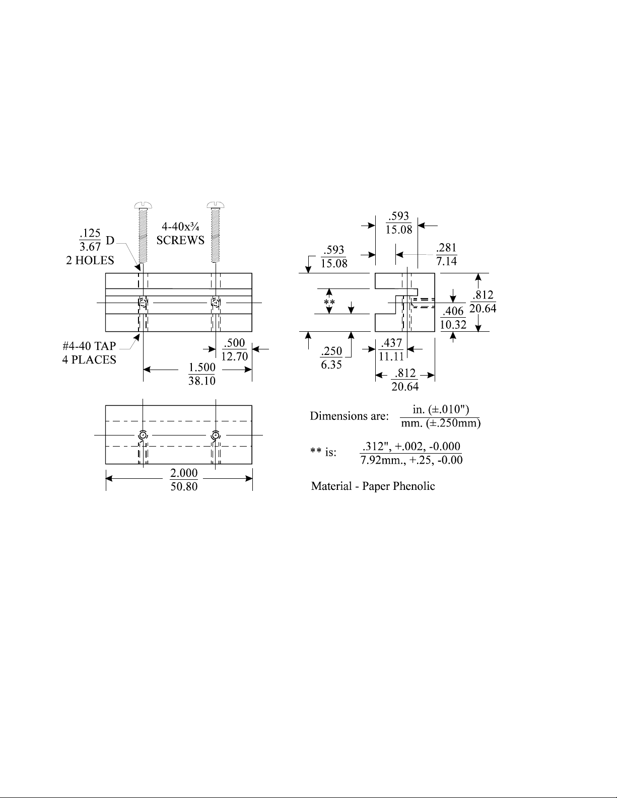
Figure A-I-1
Page 17
Page 21

APPENDIX II
POWER ENTRY MODULE
This instrument uses a Corcom, Inc. M Series Power Entry Module that combines a power inlet, switch and fusing
system in one compact unit. The IEC 320 power inlet accepts any suitably terminated cordset. The ON/OFF switch
is DPST and has international I/O markings. The selectable fuseholder allows use of single or dual European fuses
or a single North American fuse. A voltage selector provides a convenient means to change transformer primary
connections to interface with worldwide power sources.
An exploded view of the power entry module with its components identified is shown below in Figure A-II-1:
Figure A-II-1
Voltage selection:
The nominal voltage to which the power entry module is set is indicated by the indicator pin visible in one of the
holes adjacent the voltage markings.
To change selected voltage: open cover using a small blade screwdriver or similar tool; set aside cover/fuse block
assembly; pull voltage selector card straight out of housing using indicator pin; orient selector card so that desired
voltage is readable at the bottom; orient indicator pin to point up when desired voltage is readable at the bottom
(note that when the indicator pin is fixed; successive voltages are selected by rotating the card 90
voltage selector card into housing,
voltage first; replace cover and verify that the indicator pin shows the desired voltage.
Voltage selector card orientation is shown in Figure A-II-2.
printed side of card facing toward IEC connector and edge containing the desired
clockwise); insert
Figure A-II-2
279L-0401-RCA Page 18
Page 22

Fuse changing:
Figure A-II-3a
European fusing arrangement
North American fusing arrangement
Figure A-II-3b
Figure A-II-4
Fuse block/cover assembly
To change from North American to European fusing: open cover using a small blade screwdriver or similar tool;
loosen Phillips screw 2 turns; remove fuse block by sliding up, then away from Phillips screw and lifting up from
pedestal; change fuses (note that
neutral [lower] holder); invert fuse block and slide back onto Phillips screw and pedestal; tighten Phillips screw and
replace cover (note that the fuse[s] that go into the housing first are the active set.)
See SPECIFICATIONS for recommended fuses.
two European fuses are required, although a dummy fuse may be used in the
279L-0401-RCA Page 19
Page 23

APPENDIX III
HV BREAKDOWN CONSIDERATIONS
Air is subject to dielectric breakdown when the probe-to-surface spacing is small and the difference in voltage
between the probe and the surface under test is high. A destructive arc-over can occur damaging the surface under
test and/or the sensitive circuitry of the probe. Under normal operating conditions this is usually not a problem as
the probe housing is driven to a voltage essentially identical to the unknown and the difference in voltage is very
close to zero.
®
Under normal circumstances the Model 279 ISOPROBE
to its high voltage amplifier limits — a few hundred volts above its specified range of ±3000 volts.
Electrostatic Voltmeter can follow the unknown voltage up
Figure A-III-1
279L-0401-RCA Page 20
Page 24

APPENDIX IV
ACHIEVING SPACING INDEPENDENCE
Eliminating Zero Shift Over a Large Probe-to-Surface Spacing Range
This instrument’s basic operating principle is to null the electric field between a surface under measurement and the
sensitive electrode in the probe. When the potential of the surface under measurement is zero, the instrument
drives the sensitive electrode and the probe housing (a reference surface) to zero potential, thereby nulling the
electric field between the probe and the surface under measurement.
Ideally, only the surface under measurement contributes to this process. However, if other voltage sources exist in
the vicinity of the sensitive electrode, which are independent of the unknown to be measured, offsets are produced.
Such voltage sources include contact potential differences among internal probe parts, small specs of charged dust,
etc. The ZERO1 control is provided to counter such offsets by applying a voltage directly to the sensitive electrode.
The influence of these voltage sources is usually not the same at all probe-to-surface separations. Their influence
will vary in proportion to the probe-to-surface separation and will cause the instrument zero offset voltage to vary
with probe-to-surface spacing changes. This effect can be minimized to afford a high degree of zero stability over a
range of spacing changes. This is known as spacing independence.
The following procedure is used to optimize the spacing independence of the instrument:
1. Position the probe at the minimum spacing to the surface under test. Apply zero volts to the surface under
test.
2. Switch the instrument to the OPERATE mode and adjust the GAIN for a critically damped or somewhat
over-damped condition.
3. Adjust the ZERO2 control for a zero output voltage from the instrument.
4. Re-position the probe to the maximum spacing from the surface under test.
5. Adjust the ZERO1 control for a zero output voltage from the instrument.
6. Return the probe to the minimum spacing to the surface under test.
7. Repeat steps 3 through 7 until the zero shift is minimized to the desired level.
279L-0401-RCA Page 21
 Loading...