

Page 1
Projection Television
Technical Training Manual
V19-V21
V19-V21
ECHNICAL
RAINING
T
2002
DIGITAL
AUDIO
OUTPUT
EMITTER
HOME
THEATER
CONTROL
IR
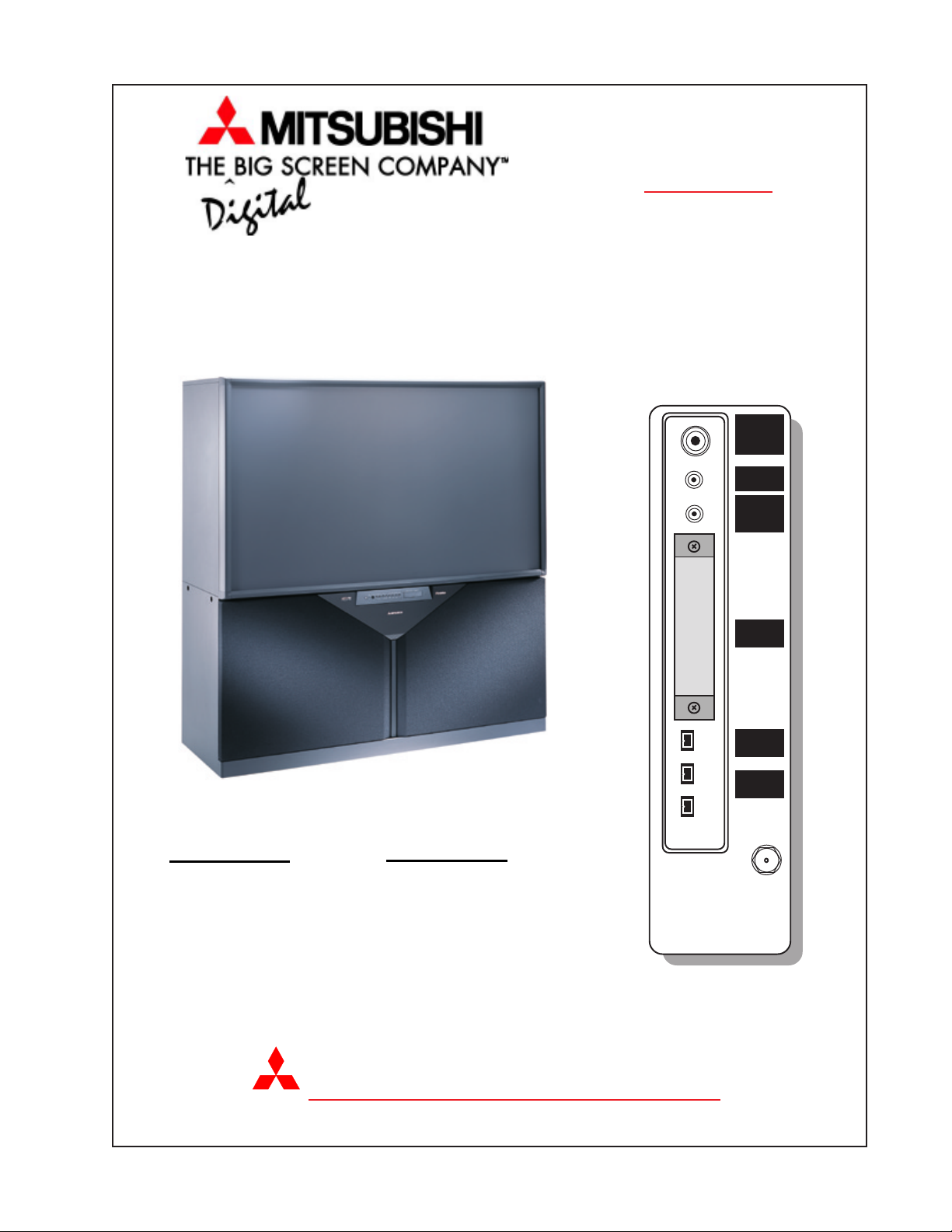
V19 CHASSIS
WS-55859 WS-48511 WS-65511
WS-55909 WS-B55 WS-65611
WS-65909 WS-55511 WS-65711
WS-65869 WS-55711 WS-65712
WS-73909 WS-73711
V21 CHASSIS
MEMORY
CARD
IEEE
-1394
INPUT/
OUTPUT
ANT-DTV
MITSUBISHI ELECTRIC
MITSUBISHI DIGITAL ELECTRONICS AMERICA, INC.
Page 2

Page 3

V19-V21 TRAINING MANUAL
TABLE of CONTENTS
Chapter 1 ... Introduction
Features ............................................................................................................ 1-1
External Inputs & Outputs .................................................................................... 1-4
Remote Control .................................................................................................. 1-6
LED Diagnostics ............................................................................................... 1-6
Chapter 2 ... NetCommand
NetCommandTM.................................................................................................. 2-1
IEEE-1394 Devices .................................................................................... 2-1
Remote Operational Mode ......................................................................... 2-1
TM
Chapter 3 ... Disassembly & PCB Location
Rear Disassembly ............................................................................................. 3-1
Light Box Removal ..................................................................................... 3-1
Chassis Removal ............................................................................................... 3-2
Main Chassis PCB Location .............................................................................. 3-2
Main Parts Location ........................................................................................... 3-2
DM Module Main Parts Location ........................................................................ 3-3
Chapter 4 ... Adjustments
Activation Codes ............................................................................................... 4-1
Adjustment Mode ............................................................................................... 4-2
Function Nomenclature ............................................................................... 4-2
OSD Position Mode ........................................................................................... 4-2
Convergence Mode ........................................................................................... 4-2
HD Convergence With No Signal ................................................................ 4-3
Chapter 5 ... Power Supply
Overall Block Diagram ....................................................................................... 5-1
Standby Supplies Switch Mode Regulator .......................................................... 5-2
Switched Supplies Switch Mode Regulator ........................................................ 5-3
On/Off Circuitry ........................................................................................... 5-3
DM Power Supply .............................................................................................. 5-5
DC Supply Source Locations ............................................................................. 5-7
Chapter 6 ... Control Circuitry
Overall Block Diagram ....................................................................................... 6-1
Input Command Circuitry .................................................................................... 6-2
Serial Data Lines ............................................................................................... 6-3
DC Supplies ...................................................................................................... 6-4
Reset Circuitry ................................................................................................... 6-4
V-Chip Blocking Circuitry ................................................................................... 6-5
AC-OFF Circuitry ............................................................................................... 6-6
Additional Inputs and Outputs ............................................................................. 6-7
1
Page 4

DM Module Control Circuitry .............................................................................. 6-7
Software Update Procedure ....................................................................... 6-9
DM Module Replacement ......................................................................... 6-10
Chapter 7 ... Video/Color Circuitry
Overall Block Diagram ....................................................................................... 7-1
NTSC Signa Selection ....................................................................................... 7-2
PCB-SIGNAL Video Color Signal Path .............................................................. 7-3
3DYC/Main Decoder Circuitry ............................................................................ 7-4
YCbCr Select Circuitry ....................................................................................... 7-5
VCJ Video/Color Signal Path............................................................................. 7-6
RGB CRT Drive & Protect Circuitry .................................................................... 7-8
Monitor Out Video/Color Signal Path .................................................................. 7-8
DM Module Video/Color Block Diagram .......................................................... 7-10
Chapter 8 ... Deflection and High Voltage
Sync Block Diagram .......................................................................................... 8-1
Sync Signal Path ................................................................................................ 8-2
Deflection and High Voltage ............................................................................... 8-3
HV 12 Volt Supply .............................................................................................. 8-4
HV Regulation .................................................................................................... 8-5
X-Ray Protect .................................................................................................... 8-5
Deflection Loss Detection .................................................................................. 8-6
Flash Protect Circuit........................................................................................... 8-7
Chapter 9 ... Sound Circuitry
Overall Block Diagram ....................................................................................... 9-1
Signal Path ........................................................................................................ 9-2
AC-3 Output ....................................................................................................... 9-3
Chapter 10 ... Convergence Circuitry
Overall Block Diagram ..................................................................................... 10-1
Waveform Generator and D/A Converter .......................................................... 10-2
LPF and Summing Amplifiers .......................................................................... 10-3
Convergence Output Circuitry ........................................................................... 10-4
Chapter 11 ...Troubleshooting Tips
Using the Front Panel LED ............................................................................... 11-1
DM Module Check ........................................................................................... 11-1
NetCommandTM Control Problems .................................................................... 11-1
CRT Phosphor Protection ................................................................................ 11-1
2
Page 5
Chapter 1
Introduction
V19 CHASSIS
WS-55859 WS-48511 WS-65511
WS-55909 WS-B55 WS-65611
WS-65909 WS-55511 WS-65711
WS-65869 WS-55711 WS-65712
WS-73909 WS-73711
V21 CHASSIS
The V19 and V21 are Mitsubishi’s high end Projection
TV chassis for 2 years. Specific models for each chassis type are listed above. Both chassis types have features not available in previous models. These features
include:
• Integrated ATV Tuner
• System 5 A/V Network
• NetCommandTM Home Theater Control
• IEEE 1394 Inputs/Outputs
• HAVi Compatibility
• 5C Copy Protection
• Record Timer for IEEE1394 D-VCR
Other features include:
• Five Picture Format modes
• Picture Format Memory by Input
• IR Repeater Outputs
• PIP-POP features (V19)
• PIP-POP and Multi PIP features (V21)
• Composite and S-Video Monitor Outputs
• Sub Picture Sound Outputs.
• Analog DTV, Component and VGA Inputs.
Differences between the V19 and V21 are software
related:
• Streamlined NetCommand Setup Menus.
• Multiple PIP.
• Different Service Menu Access Codes.
In addition to cosmetic differences, the main difference
between various models are optical improvements in the
higher end models.
1-1
Page 6
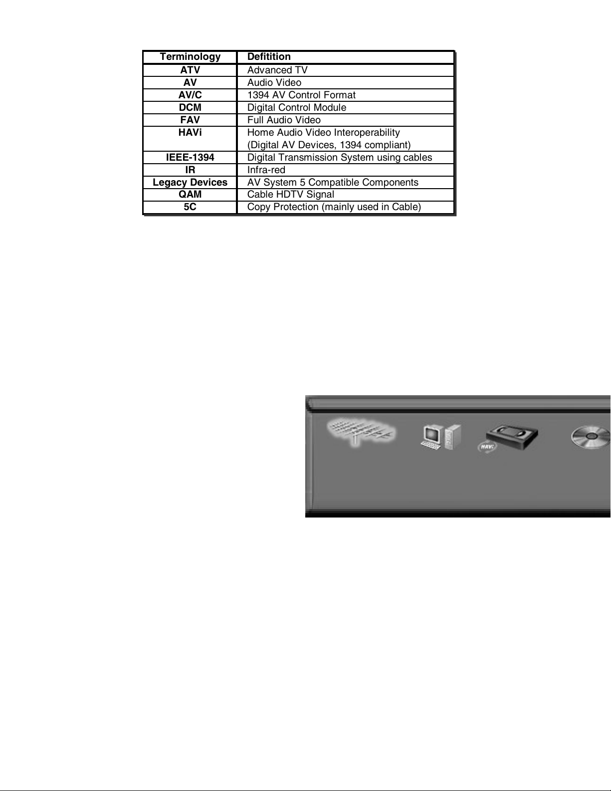
Terminology Defitition
ATV Advanced TV
AV Audio Video
AV/C 1394 AV Control Format
DCM Digital Control Module
FAV Full Audio Video
HAVi Home Audio Video Interoperability
(Digital AV Devices, 1394 compliant)
IEEE-1394 Digital Transmission System using cables
IR Infra-red
Legacy Devices AV System 5 Compatible Components
QAM Cable HDTV Signal
5C Copy Protection (mainly used in Cable)
Table 1-1: Definititions
Due to the new added features, some terminology and
abbreviations used are new. Table 1-1 lists the defini-
tions for some of the new terminology.
The Integrated ATV Tuner enables reception of
HDTV signals without using an external Set Top Box.
The ATV Tuner and its’ associated circuitry is also capable of receiving Cable QAM digital signals, when not
scrambled.
NetCommandTM simplifiies the control of Home The-
ater System devices. It controls compatible analog, digital and HAVi components using only the TV layer of the
Remote Control.
When the Remote “Device” button is pressed an onscreen display shows all devices in that Home Theater
System. An example of a Device Select Display is shown
below.
The user selects the device using the “Direction” buttons, then presses “Enter”. Compatible devices are activated and corresponding input selections are automatically performed. The initial NetCommandTM setup procedure is described in Chapter 2.
NetCommandTM controls Home Theater components
by two methods:
1) Legacy Devices (System 5 compatible) are
controlled through IR Blasters connected to the
System 5 IR Output Jacks.
2) IEEE-1394 compatible components are
controlled over cables connect to the 1394
Jacks.
Ant A
Ant A
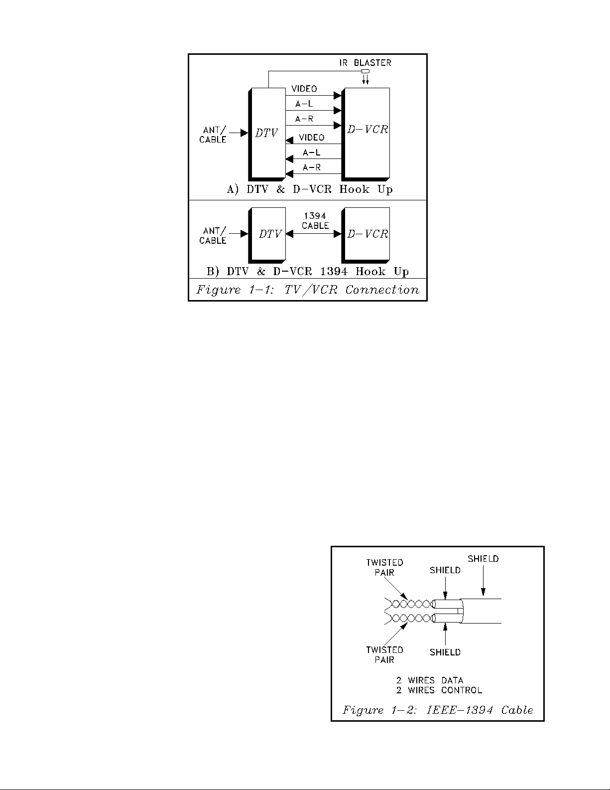
IEEE-1394 is a system used to transmit digital data
PC D-VHS DVD
streams over cable. The system may also be referred
to as “Firewire®”. Basically it can be considered a pipe-
line to transfer digital information from one unit to an-
other.
Device Select Display
1-2
Page 7
When used with consumer Audio Video products it
transfers digital data streams for DTV and Digital Cable
Boxes. This includes MPEG2 HDTV data streams.
When components are 1394 compatible, interconnection of the units is simplified. Figure 1-1 illustrates how
the 1394 system simplifies interconnection between the
DTV and a D-VCR.
Figure 1-1A shows the connections between a DTV
and D-VCR when components are not 1394 compatible. Six cables are required to transfer analog signals
from one unit to the other. In addition, control of the
VCR would be from an IR Blaster signal or directly
from the D-VCR’s Remote.
Figure 1-1B shows a single 1394 cable connection between a DTV and the D-VCR that are 1394 compliant.
There are two types of 1394 Cables:
• 6 wire – two wires for data transfer, two wires
for timing, and two wires for power.
• 4 wire – two for data transfer and two for
timing.
tion between conductors. 1394 cables may be up to
40 feet in length.
Home Theater components that are not System 5
or 1394 compatible can usually be controlled through
the TV by one of two methods.
1) Using the corresponding Mitsubishi remote
layer, Cable, VCR, DBS or DVD.
2) Using that component’s Remote Control and an
IR Blaster connected to the IR Repeater Jacks.
5C Copy Protection
5C Copy Protection prevents copying restricted signals. There are three levels of 5C Copy Protection:
1) Unlimited Recording allowed.
Figure 1-2 shows an IEEE-1394 4 wire cable, used in
consumer Audio Video. It consists of two pairs of
twisted wires. Each pair is separately shielded, and then
the entire cable is shielded. This minimizes any interac-
1-3
Page 8
2) One Recording allowed.
3) No Recordings allowed.
At present, only QAM (Digital Cable Signals) are coded
with 5C Copy Protection. When the V19 detects a
Copy Protected signal, that signal is not output at the
Monitor Outputs of the TV.
Monitor Output Sources
There are only two sources that output signals at the
Monitor Outputs, NTSC signals and signals from the
ATV Tuner (when not Copy Protected).
Timer Recording
Mitsubishi's HS-HD2000U and HS-HD1100U, DVCRs includes HDTV recording capability and HAVi.
However it must be connected to an external ATV Receiver with a IEEE-1394 interface, such as in the V19
chassis. Time Shift Recording allows recording from
the V19’s ATV Tuner without turning the TV On, only
the TV’s signal circuits are activated. The Time Shift
Recording time can be pre-programmed so the user does
not have to be present to activate the recording.
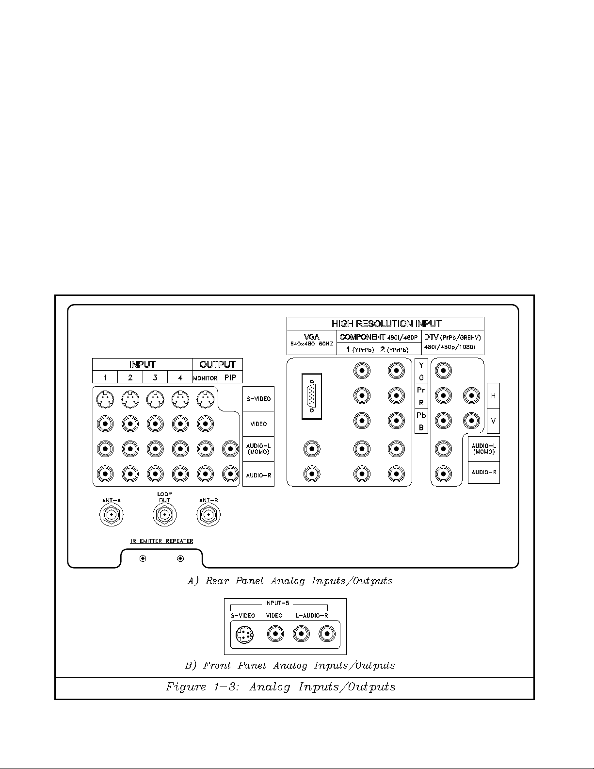
External Inputs & Outputs
Analog External Inputs and Outputs are located both
on the rear and front of the TV. Figure 1-3 shows the
External Analog Inputs and Outputs. The DTV Inputs
1-4
Page 9
are still available even though a Set Top Box is not needed
to receive HD broadcasts. In the V19 these inputs are
mainly used to connect a Digital Broadcast Satellite
(DBS) to the TV.
The IR Emitter Repeater outputs are for connecting IR
Blasters to control AV devices that are not System 5 or
1394 compatible. Signals from other manufacturer’s
remotes are amplified in the TV and output from the
Repeater Jacks.
• ANT-DTV … Antenna or Cable Input (ATSC
or QAM)
• Three 1394 Jacks … to connect external 1394
compatible devices
• Two System 5 IR Emitter Jacks … for IR
Blasters controlling external System 5 devices.
• Digital Audio Output … AC-3® digital output
for connection to an external device with an
AC-3® Decoder.
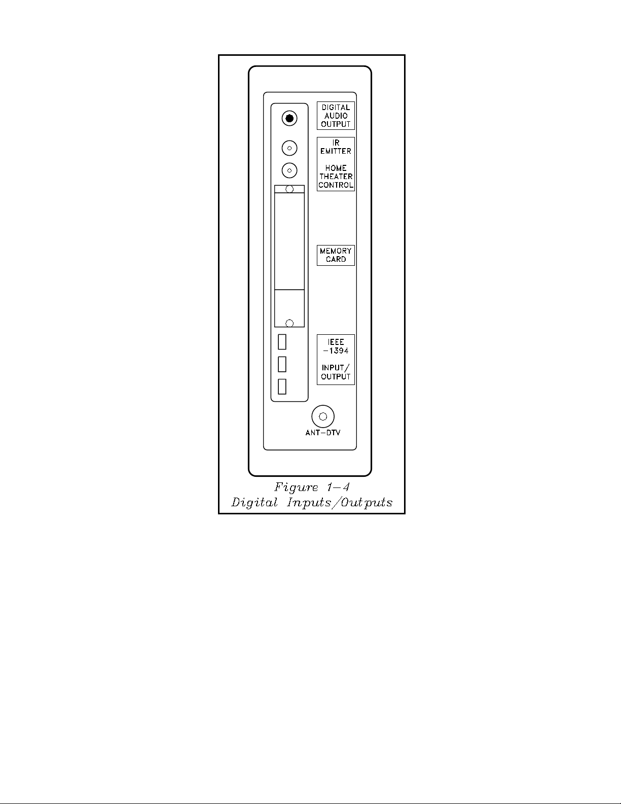
Digital Analog Inputs & Outputs are located on the
rear of the TV and are shown in Figure 1-4. These
include:
Display Formats
Figure 1-5 illustrates the Display Formats possible in
the V19. Pressing the “FORMAT” button on the Re-
mote Control changes the Display Format. Note that
1-5
Page 10
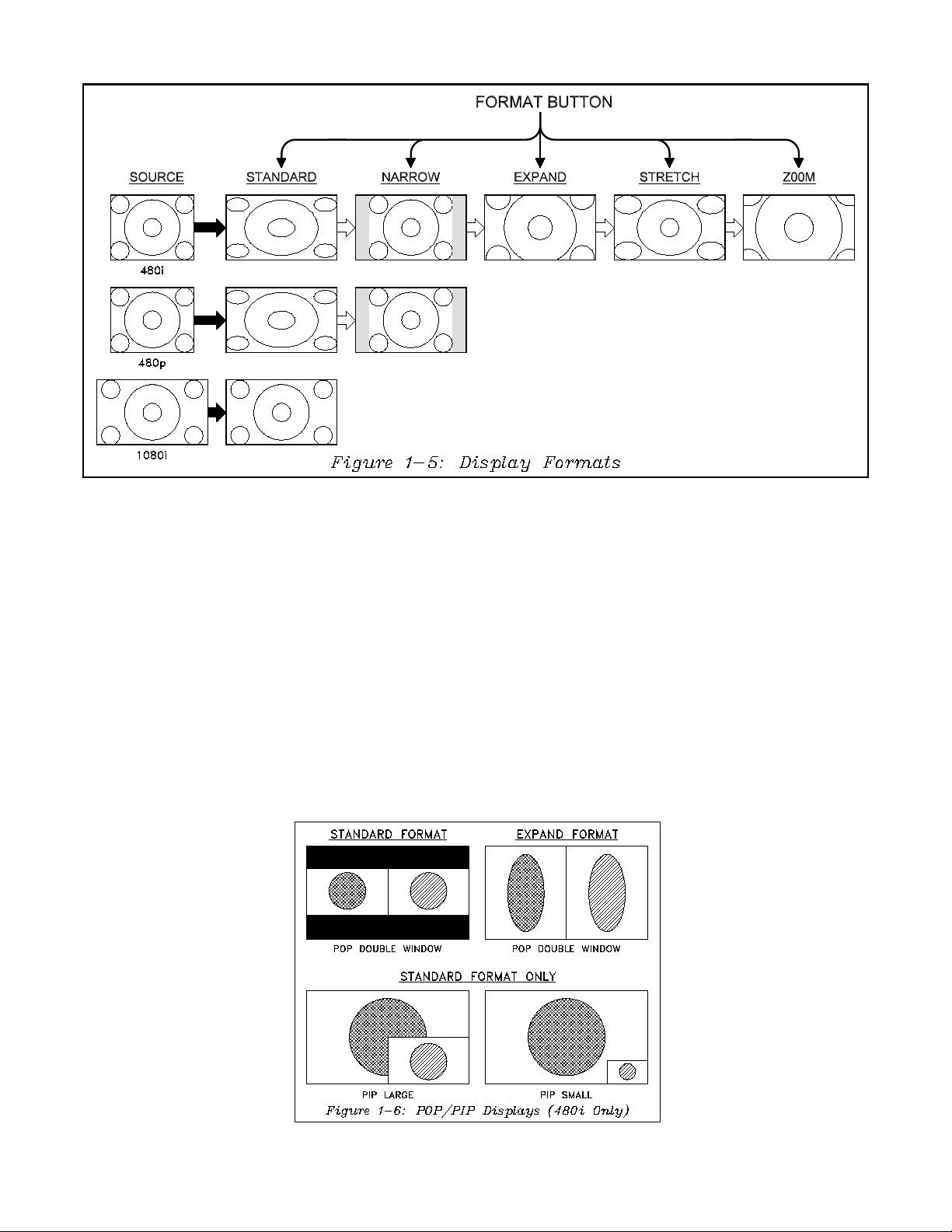
all five Display Formats can only be accessed when the
signal source is 480i. When the source is 480p, only
Standard and Narrow can be activated, and when the
source is 1080i only Standard is available.
PIP-POP V21 has multi-PIP capabilitys. Only 480i
format signals can be selected for POP/PIP main and
sub pictures. POP pictures can be viewed in either the
“Standard” or “Expand” format.
The Format memory is by input. When a Display Format is selected for an Input, that format will be activated
when that input is selected again.
POP/PIP Features
POP/PIP features are illustrated in Figure 1-6. They
are similar to those in previous models. In addition to
In the Standard Format main POP pictures are symmetrical and there are dark areas at the top and bottom
of the picture. In the Expand Format, the main picture
is compressed horizontally and stretched vertically, removing the black areas.
Remote Control
1-6
Page 11
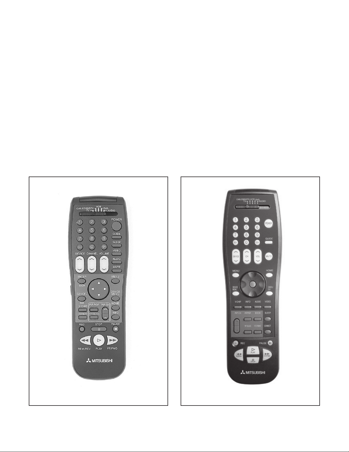
The Remote Hand Unit for the V19 appears the same
as that in previous models, refer to Figure 1-7. However there are two differences.
• The "INPUT" button is changed to "DEVICE".
• There are two operational modes, Standard
and NetCommandTM.
The Remote for the V21 is physically larger but has the
same basic functions. See Figure 1-8.
The Remote Hand Unit comes in the Standard Mode
so the TV can be controlled in the normal fashion. To
use NetCommandTM, the Remote Hand Unit must be
changed to the NetCommandTM mode. Changing the
Remote operational mode is described in Chapter 2.
LED Diagnostics
The LED Diagnostic Mode, used in some previous
models is carried over in the V19 and V21 with some
additional features. This helps isolate the source of shutdown problems by counting how many times the front
panel LED flashes. For details on this feature, refer to
Chaper 11.
AC-3® is a registered trademark of Dolby
Laboratories, Inc.
FireWire® is a registered trademark of
Apple Computers, Inc.
Figure 1-7: V19 Remote
Figure 1-8: V21 Remote
1-7
Page 12

1-8
Page 13
Chapter 2
NetCommand
The NetCommandTM feature in the V19 and V21 is an
enhanced user simplified Home Theater Control System. It provides graphic control of an entire Home Theater System through the TV. It controls existing analog
devices along with New Digital Home Theater devices.
NetCommandTM uses System 5 to control Home
Theater components with IR Blasters, and also controls HAVi capable devices over 1394 cables.
When a TV is first installed, the Setup Wizard automatically displays a series of Initial Setup Screens to configure System 5. It allows entry of all devices connected
to the TV. When the Initial Setup is complete,
NetCommandTM is automatically activated. For specfic
instructions on setup and use, refer to the Owner's Guide
and NetCommand Guide.
TM
IEEE-1394 Devices
The TV automatically detects when an IEEE-1394 device is connected. The user will be asked to select a
name for that device that will be displayed in the Device
menu.
Remote Operational Mode
Before the NetCommandTM feature can be use, the Remote Hand Unit must be set to the NetCommand
operational mode. To change to the NetCommand
mode:
• Set the Remote to the TV Layer
• Point the Remote away from the TV
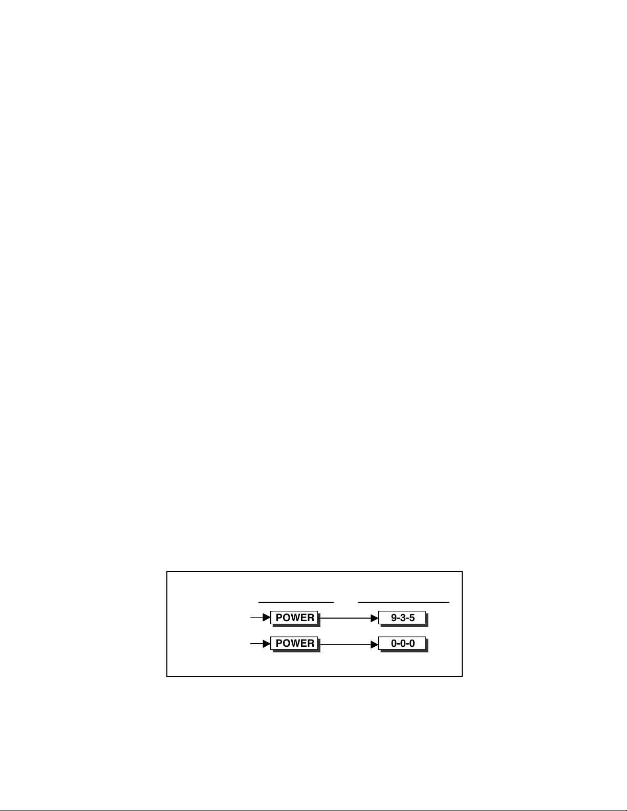
• While holding the "Power" button, press "9-35" in sequence.
Figure 2-12 illustrates how to change to the
NetCommand
TM
mode, or to the Standard mode.
TM
TM
Set the Remote to the TV Layer
Press and Hold
NetCommand POWER 9-3-5
Standard POWER 0-0-0
Figure 2-12: Change Remote Operation Mode
2-1
Press in Sequence
Page 14

2-2
Page 15
Chapter 3
Disassembly & PCB Locations
There are no radical changes in the disassembly of
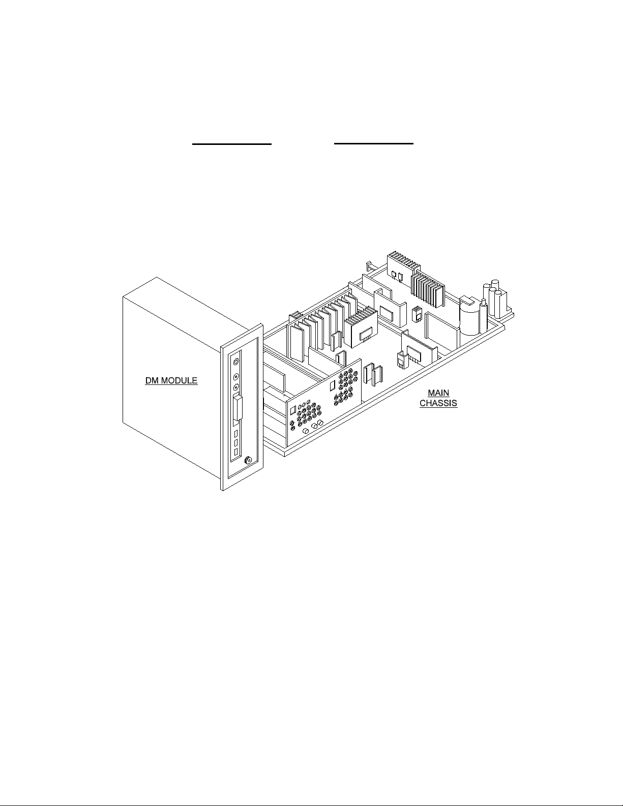
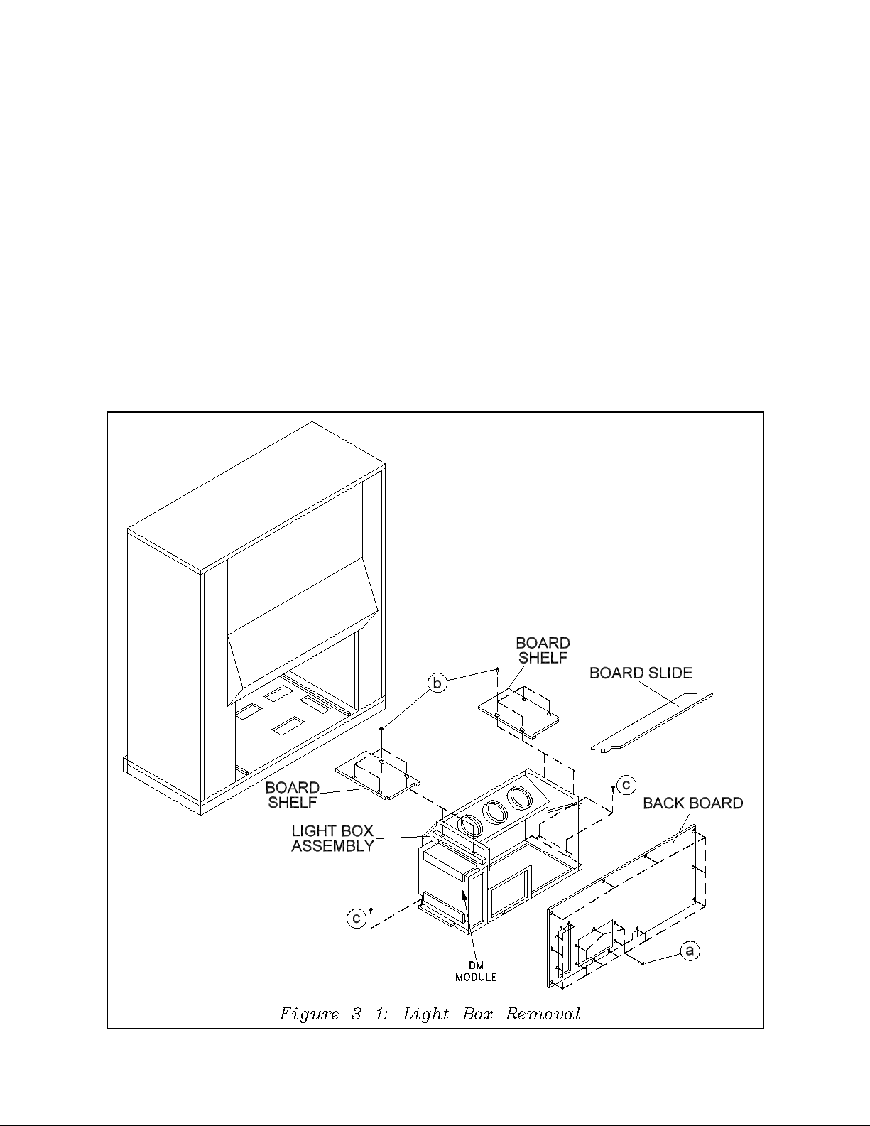
V19 models. Figure 3-1 shows the cabinet rear disassembly for V19 models. The Light Box is still removable as a unit, as shown in Figure 3-1. Of course
all front panel PCBs and the speakers must be disconnected before the Light Box can be removed.
Figure 3-1 shows one major change to the Light Box
assembly, the addition of the Digital Module (DM)
on the left side. The ability to remove the CRTs,
main chassis and DM as a unit, facilitates servicing.
Only the Light Box is needed to troubleshoot most
problems. So only the Light Box can to be taken to
the shop, rather than the complete set.
3-1
Page 16
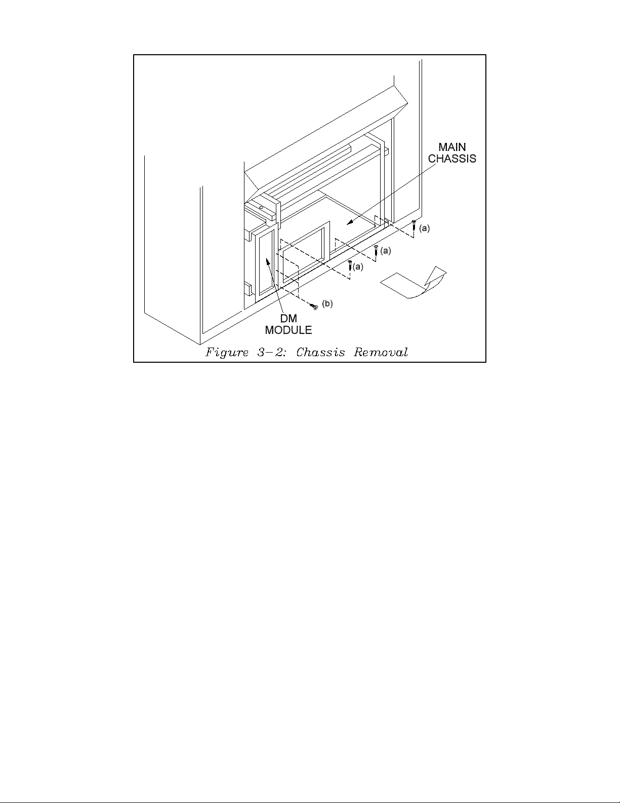
Accessing The Main Chassis
The Main Chassis can still be accessed as is in previous models.
1) Loosen wire ties on cables to the CRTs, front
panel, speakers, etc.
2) Remove the three chassis mounting screws
(a), shown in Figure 3-2.
3) Release the chassis locks on the front of the
chassis, shown in Figure 3-3.
4) Slide the chassis out the rear of the cabinet.
The DM Module is attached and will slide
back with the chassis.
5) Tilt the chassis upward to access the bottom
of the PCBs.
In some cases, Cable length will not allow the DM
to slide back with the chassis. If this occurs:
1) Remove the three DM mounting screws (b),
in Figure 3-2.
2) Slide the DM Module out the rear of the
unit.
3) Then slide the chassis out the rear of the
unit.
NOTE: The DM Module must be connected to the
main chassis, or the TV will not switch On.
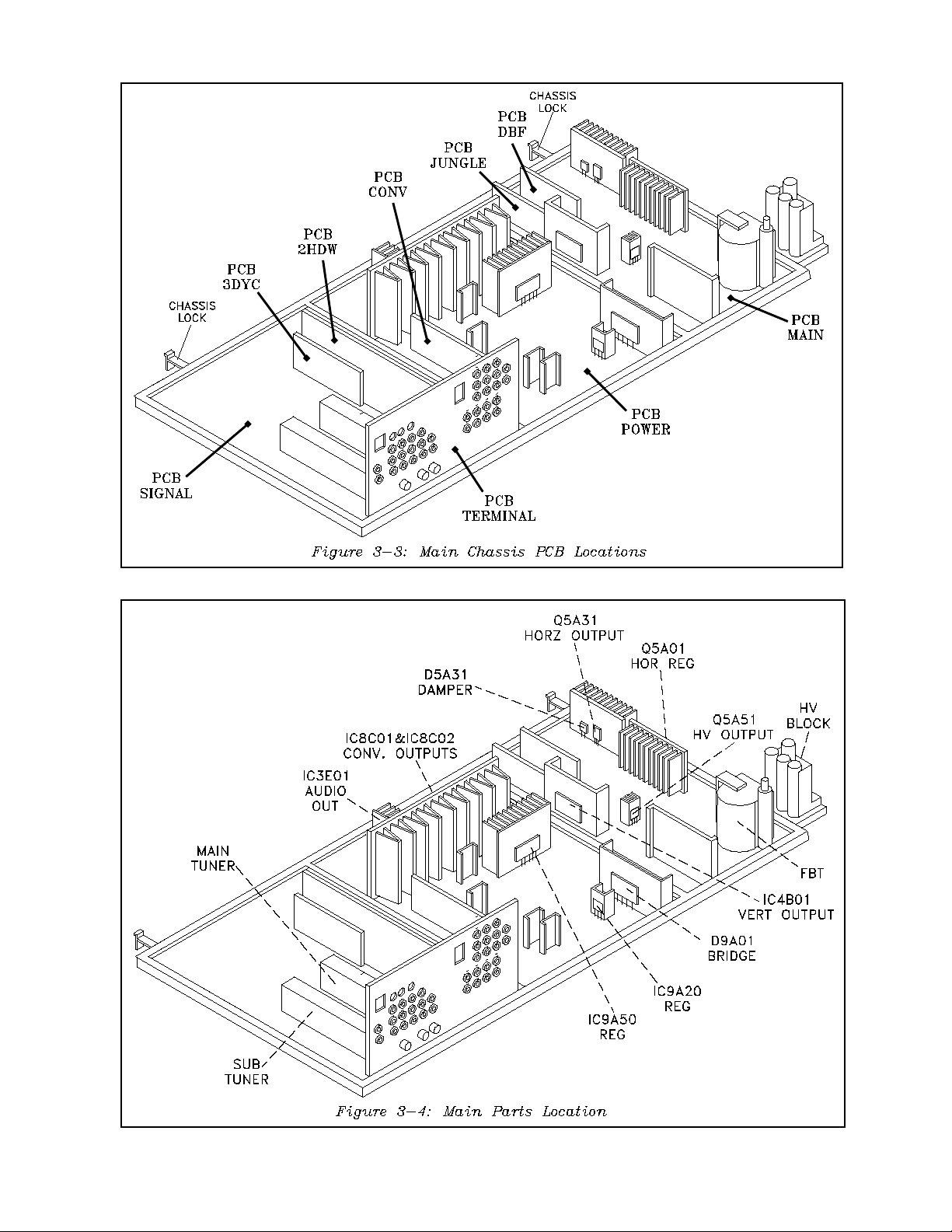
Main Chassis PCB Locations
Figure 3-3 shows the location of PCBs that comprise the main chassis. The following PCBs are plug
in and are considered replaceable components:
• PCB-3DYC
• PCB-2HDW
• PCB-CONV-GENE
• PCB-JUNGLE
• PCB-DBF
PCBs SIGNAL, POWER and MAIN are not considered replaceable, an troubleshooting must be to
component level.
Main Parts Location
For a reference, Figure 3-4 shows the location of
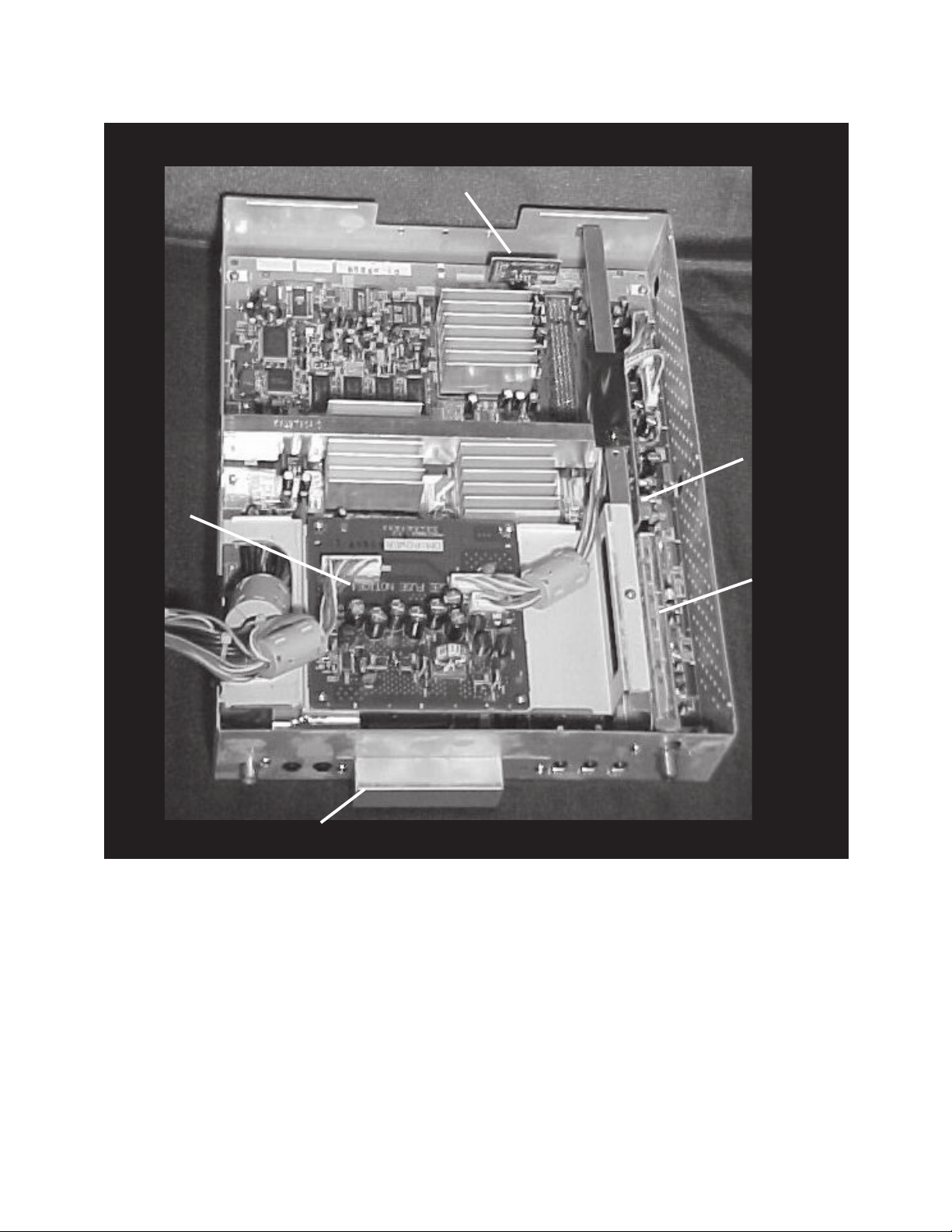
the major components in the main chassis. Figure 3-
5 displays the component layout inside the DM.
3-2
Page 17
3-3
Page 18
DM
POWER
SUPPLY
E2P
MODULE
DE-
MODULATOR
ATV
TUNER
FLASH CARD
SLOT COVER
Figure 3-5: DM Module Main Components
3-4
Page 19
Chapter 4
Adjustments
Chassis Option Menu Adjustment Mode Convergence Mode OSD Position
VZ5
VZ6
VZ7
VZ8
VZ9
V15
V16
V17
V18
V19
V20
VK20
V21
1-3-7-0 2-3-5-7 2-3-5-9 <6><5><4> Adjust Mode
"" " "
1-2-7-0 1-2-5-7 1-2-5-9 <6><5><4> "
"" " "
0-1-7-0 0-1-5-7 0-1-5-9 <6><5><4> "
1-3-7-0 2-3-5-7 2-3-5-9 <6><5><4> "
1-2-7-0 1-2-5-7 1-2-5-9 <6><5><4> "
8-2-7-0 8-2-5-7 8-2-5-9 <6><5><4> "
0-1-7-0 0-1-5-7 0-1-5-9 <6><5><4> "
0-1-7-0 0-1-5-7 0-1-5-9 <6><5><4> 0-1-8-8
2-2-7-0 2-2-5-7 2-2-5-9 <6><5><4> Adjust Mode
2-2-7-0 2-2-5-7 2-2-5-9 <6><5><4> Adjust Mode
2-1-7-0 2-1-5-7 2-1-5-9 <6><5><4> 2-1-8-8
Table 4-1: Service Menu Access Codes
The individual Adjustment Procedures for the V19 and
V21 are basically the same as in previous models, and
are described in the Service Manual. Therefore, they
don't require repeating here. There are some changes
in the Adjustment Procedure process in the V19/V21
Chassis. The changes iclude:
• Change in the "Mode Activation Codes".
• Change in On-screen nomenclature of some
"Adjustment Functions".
• New OSD Position Adjust Mode.
• Change in the procedure to activate the
"Convergence HD Mode" with no signal.
The OSD Position Mode is new. In previous models,
OSD position was set in the HR Function of the
Adjustment Mode. The V19/V21 uses a separate
mode, with its' own activation code to position the OSD.
Activation Codes
For a quick reference, Table 4-1 lists the codes for the
V21 and previous chassis types.
4-1
Page 20
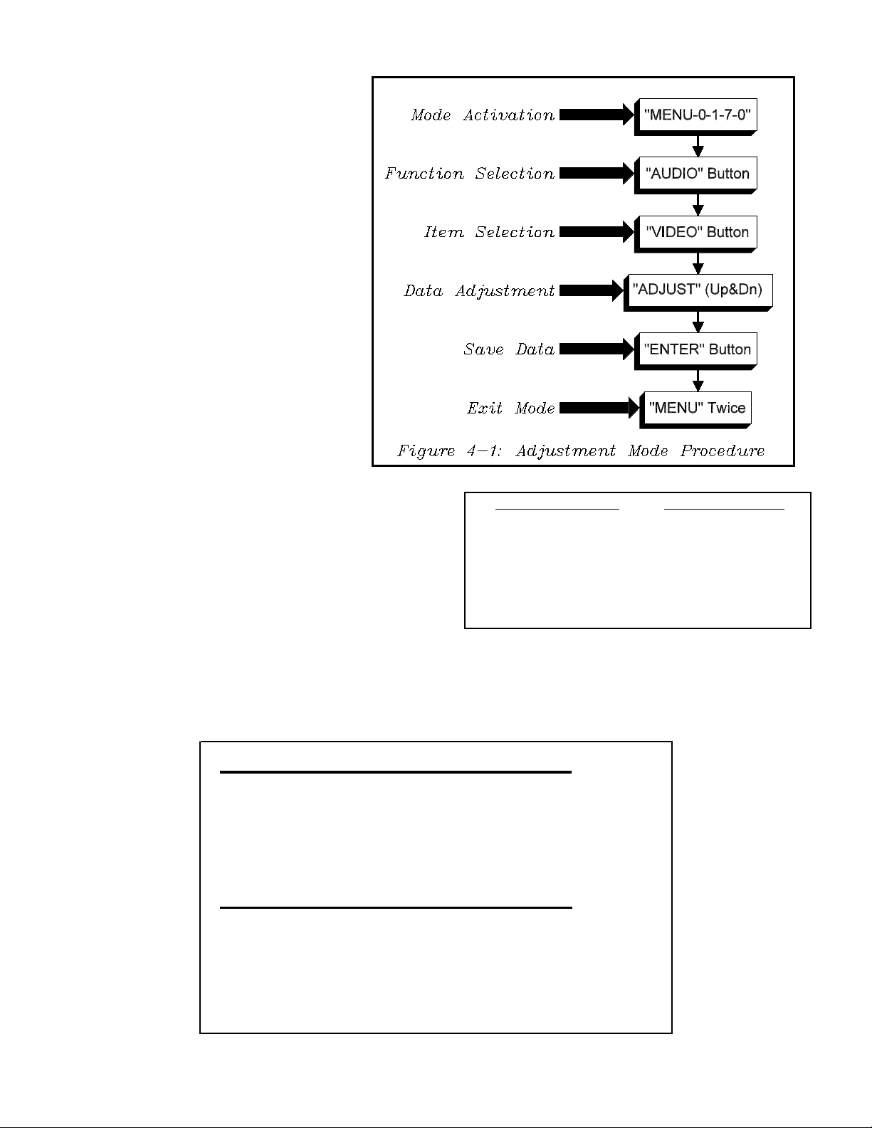
Adjustment Mode
Outside of the activation code, the procedure
for the "Adjustment Mode" is the basically
same as in previous models. Figure 4-1 illustrates the "Adjustment Mode" procedure.
One of the changes in the "Adjustment Mode"
is the on screen nomenclature used for some
of the "Adjustment Functions. The changes
are shown in Table 4-2
In the Adjustment Mode VC Function,
pressing "3" toggles the signal mode between 480i, 480p, 1080i, DM and VGA.
DM is an added signal format, but is only
available for possible future use. When "3"
is pressed, data changes are not automatically saved. Therefore, press "ENTER"
save data before pressing "3".
OSD Position Mode
The horizontal position of the OSD is set in this mode.
The OSD Position must be set in both the SD (Standard Definition), and HD formats. The procedure for
setting OSD Position is given Figure 4-2.
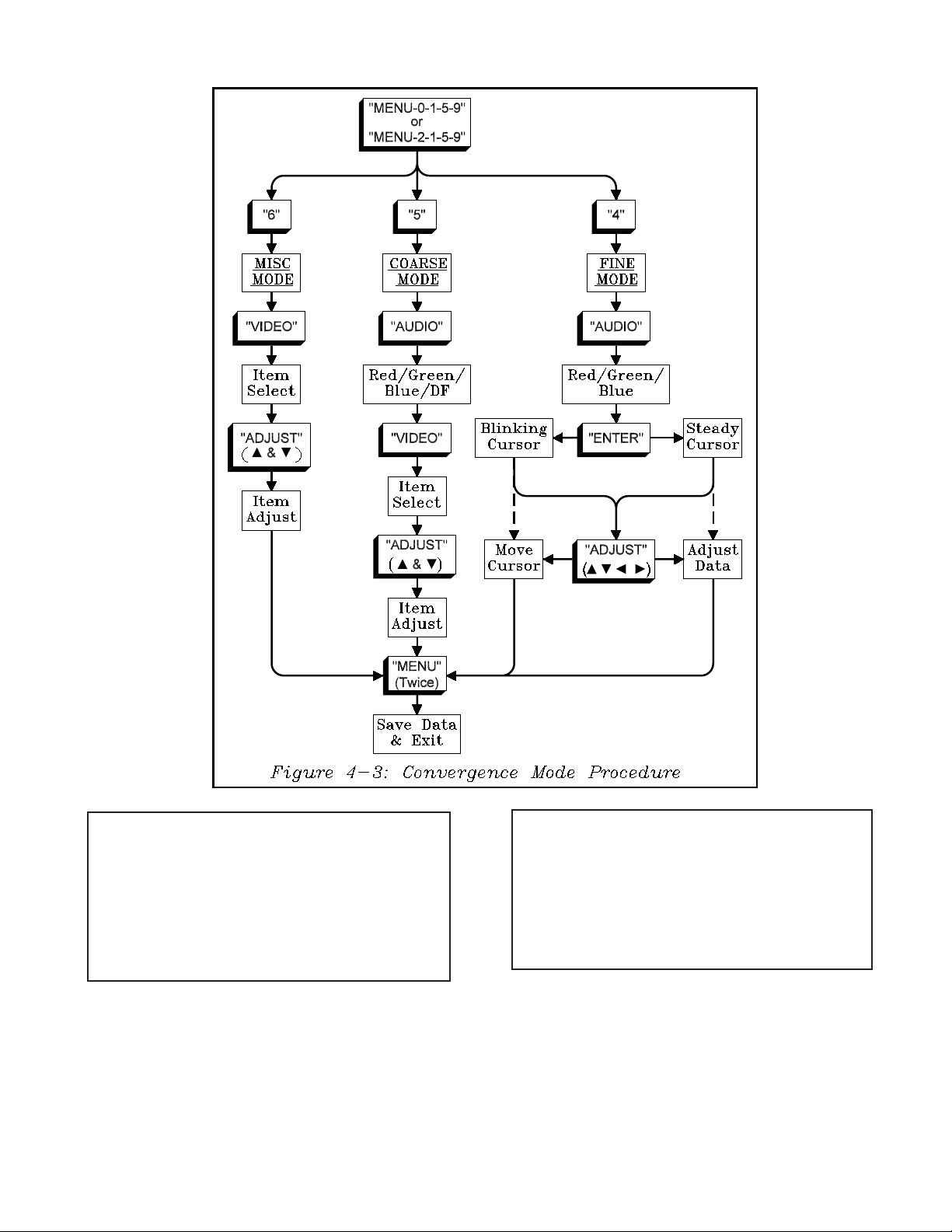
Convergence Mode
Like the "Adjustment Mode" the only change in the
"Convergence Mode" procedure is the activation
code. Figure 4-3 graphically shows the general "Convergence Mode" procedure.
SD OSD Horizontal Position Procedure
1) Selec t an NTSC s ignal (A nt-A or A nt-B).
2) Press "M E NU-0-1-8-8" or "MENU-2-1-8-8"
3) Use the Adjust Buttons to adjust OSDSD data to c enter the
On Screen Display.
4) Press "M ENU" to s ave data and exit the mode.
HD OSD Horizontal Position Procedure
1) Selec t an HD signal (DTV Inputs).
2) Press "M E NU-0-1-8-8" or "MENU-2-1-8-8"
3) Use the Adjust Buttons to adjust OSDHD data to center the
On Screen Display.
4) Press "M ENU" to s ave data and exit the mode.
Previous Models V19/V21 Chassis
Video/Chroma VC
Jungle JNGL
Main Matrix MNTS
Sub Matrix SNTS
Audio AUD
Table 4-2: Adjustment Function Changes
One additional change is the procedure on how to activate the HD Convergence Mode when no HD signal is
available
Figure 4-2: OSD Position Adjustment Procedure
4-2
Page 21
Note: In an Adjustment Mode, if the data
changes too fast ... Change the Remote to the
NetCommandTM mode. (Hold "Power" and
press "9-3-5" in sequence).
Caution: When adjustments are complete,
change back to the Standard Mode. (Hold
"Power" and press "0-0-0" in sequence.
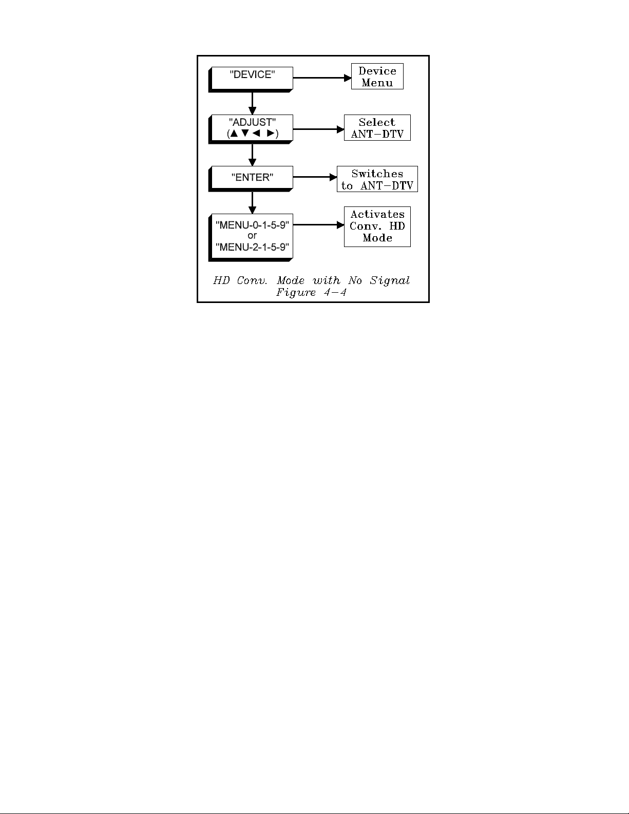
HD Convergence Mode With No Signal
Although HD Test Patterns are required to perform
Centering and Static Convergence, it is possible to perform Coarse and Fine Convergence Adjustments when
no HD signal is available.
Note: To produce the internal crosshatch with
a black background:
1) Turn off Video Mute.
2) Select a source with no signal.
3) Activate the Convergence Mode.
With Video Mute On, only a blue raster is produced.
The procedure for activating the HD Convergence Mode
with no HD signal, is easier than that used in previous
models. Merely select ANT-DTV as the signal source
and then enter the Convergence Activation code. The
Convergence Mode comes on in the HD mode. Fig-
ure 4-4 graphically illustrates this procedure.
4-3
Page 22
Adjustments
Refer to the Service Manual for specific adjustment procedures.
4-4
Page 23

Chapter 5
Power Supply
The above block diagram shows the main sections
of the Power Supply circuitry. As in previous models, two types of DC supplies are generated, Standby
and Switched. Standby supplies are generated as
long as the TV is connected to an AC power source.
Switched supplies are activated when the TV is
switched On.
Switch Mode Regulators are the source for both types
of supplies. An additional Standby source is used to
supply power to the DM Module in the V19/V21 chas-
sis. The DM Power Supply is internal to the DM Module. It receives power from the Standby 12V supply
and generates DM 3.3V and DM 5V supplies. The
two DM supplies fall into the Standby category and are
present as long as the TV is plugged in.
The Standby and Switched supplies shown in the diagram are only those directly generated by the Switch
Mode Regulators. Additional DC supplies are generated from those shown above.
5-1
Page 24

Standby Supplies Regulator
Figure 5-1 illustrates the Standby Switch Mode Regulator. Since its’ operation is similar to that in previous
models, a lengthy description is not required. Key points
of operation are:
1) D9A01 supplies DC power to the regulator.
2) Start up voltage (16 volts) is supplied by
R9A22 to pin 4 of IC9A20.
3) The signal at pin 2 of T9A20 is rectified by
D9A22 and adds to the voltage at pin 4 of
IC9A20. If the voltage drops below 11 volts
the oscillator shuts Off.
4) Feedback for regulation is from the STBY 12V
supply through IC9A21 and PC9A20 to pin 5
of the IC9A20.
5) Over Current Protection is provided by
directing the voltage at the pin 2 (Source
ground return) to pin 5 of the IC. A sudden
increase in voltage will shut down the oscillator.
6) Pin 4 of the IC, the oscillator’s DC supply
input, also provides Over Voltage Protection.
If the voltage at pin 4 exceeds 20.5 volts the
oscillator shuts down.
5-2
Page 25

DC Standby supplies are generated in the secondary
circuits of T9A20, these include STBY 6V, STBY
12V and STBY 32V. STBY 5V supplies are derived from the STBY 12V, and STBY 28V from the
STBY 32V.
The STBY 12V and STBY 32V supplies are generated by rectifying the same secondary winding signal.
Figure 5-2 illustrates how this is accomplished. The
positive part of the signal from the secondary winding is rectified by D9A30 to generate the STBY 12V
supply. The same signal is directed through C9A32
to the anode of D9A32. The anode of D9A32 is
clamped at 12 volts by D9A31 and the 12 volt supply. The combination of the clamping action and
rectification of the signal from C9A32 generates the
STBY 32V Supply.
CAUTION: The primary section of the regulator is
referenced to a Hot Ground. Use an Isolation
Transformer when working in the Primary circuitry.
Note in Figure 5-1, that voltage sources rectified by
D9A01, and D9A27 are both directed to the Switch
Mode Regulator for the Switched Supplies .
Switched Supplies Regulator
Figure 5-3 shows the Switched Supplies Switch Mode
Regulator. Except for component nomenclature its’
operation is the same as the Standby Regulator.:
1) Startup and the oscillators DC supply are input
at pin 4 of IC9A50.
2) The SW 110V supply is monitored for
regulation and is directed via IC9A51 and
PC9A51 to pin 1 of IC9A50.
3) Switched supplies are generated by rectifying
secondary winding signals.
On/Off Circuitry
Due to the V19/V21 Time r Recording feature, two On/
Off commands are required. Time Shift Recording enables using the TV's Tuner as the signal source for a
VCR pre-programmed recording, without switching the
TV completely On.
The On/Off circuitry is also shown in Figure 5-3.
There are two Power On commands, P-ON1 and PON2. P-ON1 activates the Standby Regulator,
IC9A50. IC9A50 generates 220V, AUDIO (17V),
+24V, -24V and 110V Switched Supplies. P-ON2
activates the 12V and 5V Switched Supplies, which
supply power to the signal processing circuitry.
5-3
Page 26
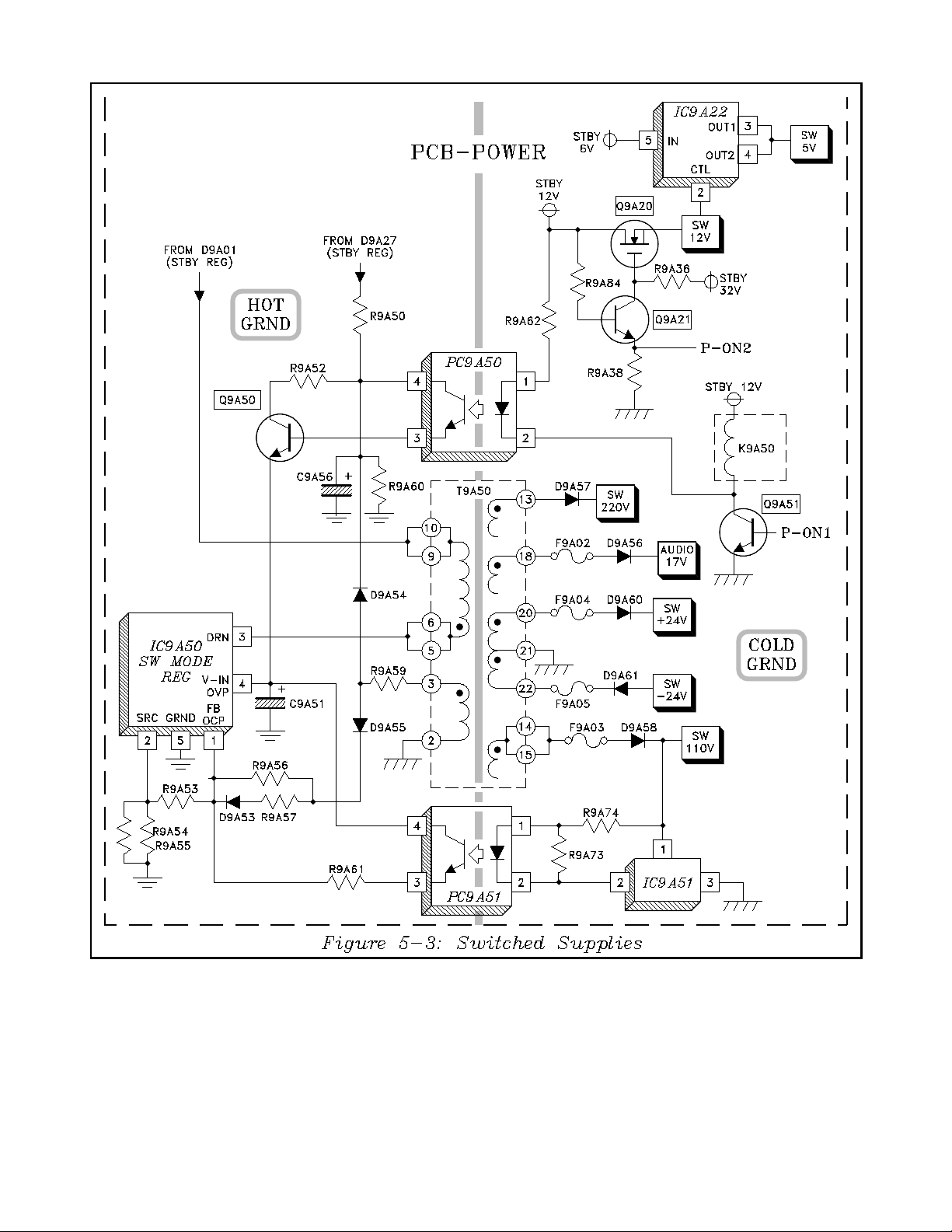
When the P-ON1 line goes High the turn On sequence
is:
• Q9A51 conducts
• Relay K9A50 closes, removing current
limiting resistor R9A02 (refer to Figure 1).
• The LED and Photo Transistor in PC9A50
conduct.
• Q9A50 conducts supplying rectified voltage
from D9A27 in the Standby Regulator to pin
4 of IC9A50.
• Additional voltage is added to the Startup
voltage by rectifying the signal at pin 3 of
T9A50 and directing it to the collector of
Q9A50.
5-4
Page 27
When P-ON2 goes High, it turns Q9A21 Off:
• Allowing Q9A20 to conduct, generating the
SW 12V supply.
• The SW 12V supply enables IC9A22, which
outputs the SW 5V supply.
At a pre-programmed recording time, using the TV
as the Signal source, only the P-ON2 line goes High.
This activates only the signal processing circuits in
the TV.
DM Power Supply
Figure 5-4 illustrates the DM Power Supply, which
is located on a separate PCB in the DM Module.
STBY 28V and STBY 12V from the Main Standby
circuitry are input to the DM Power Supply. Both
voltages are routed to the digital circuitry in the mod-
ule. The STBY 12V also provides power for the Regulator circuitry in the DM Power Supply.
The DM Regulation circuitry generates two supplies
DM 5V and DM 3.3V. The Regulator consists of
four ICs, IC9B00, Q9B00, Q9B01 and Q9B02.
IC9B00 is a Pulse Width Modulator (PWM), and
Q9B00, Q9B01 and Q9B02 are comprised of
MOSFET transistors. Multiple Drain and Source
connections are used to increase current handling capability.
Q9B00 and Q9B01 are connected in a push-pull configuration. Gate drive is generated in IC9B00.
UGATE drives Q9B00, and LGATE drives Q9B01.
The output of the push-pull circuit is at the junction
Q9B00 Source and Q9B01 Drain. The output is filtered to generated the DM 3.3V supply.
5-5
Page 28

A sample of the 3.3V supply is fed back to pin 5 of
p
(
)
(sig
)
(sig
)
IC9B00 for regulation. Regulation is achieved by
controlling the PWM of the Gate drive signals.
The push-pull circuitry output is also used to generate the DM 5V supply. The signal, before filtering,
is stepped up by T9B00, but is not large enough to
All current rated in mA.
Name
Voltage3.33.33.33.355555-9999
3DYC
Ant.
Relay
Audio
Am
Audio
Process
AV
Switch
Conv.
Gen
Conv.
Out
CRT
(video)
DBF
Digital
Module
CRT
HV
H-Defl
Jungle
TV µPC
V-Chip
Sub
Misc
(main)
Preamp
1
3.3V23.3V33.3VS15V15V25V35VS15VS
3.3V
200 25 105
120 5050 5050
3500 600
30
generate 5 volts. To generate 5 volts the secondary
winding is clamped at 3.3 volts by Q9B02.
The LGATE output of IC9B00 supplies Gate drive
for Q9B02. When Q9B02 conducts it clamps the
Drain outputs to 3.3 volts. The clamping at 3.3 volts
and the stepped up signal from T9B00 are filtered to
form the DM 5V supply.
2
-9V
87 10
20
9V
1
9V29V
85
150
180
3
Protect
AMDP
Sub
Decoder
SVM
Switch
nal
Tuner
(DM)
Tuner
nal
V-Defl.
2H
Enhance
Video
Chroma
600 270 111
75
130 100
30 280
200 60
140
Table 5-1: V19 Power Distribution Estimate (3.3V to 9V Supplies)
5-6
Page 29

DC Supply Source Locations
p
(
)
(
)
(
)
(sig
)
(DM)
(sig
)
The DC supplies shown in Figures 5-1 and 5-3 are
located on the PCB-POWER. Additional supplies
are generated from these supplies on other PCBs. In
the Service Manual DC Supplies are designated with
a "V" or "VS".
• "V" designates a Switched Supply (5V)
• "VS" designates a Standby Supply (5VS)
Table 5-1 shows the Power Distribution for the 3.3V
through 9V supplies, and Table 5-2 for the 9VS to
220V supplies. The tables indicate the estimated
current, in Ma, supplied to the various circuits. When
there is more than one supply of the same value, a
superscript number is added to those supplies. For
instance, 3.3V1 and 3.3V2 are different supplies.
All current rated in mA.
Name
Voltage 9 12 12 12 17 -24 24 28 32 110 220 6.3
3DYC
Ant.
Relay
Audio
Am
Audio
Process
AV
Switch
Conv.
Gen
Conv.
Out
CRT
video
DBF
Digital
Module
CRT 630
HV
H-Defl
Jungle
TV µPC
V-Chip
Sub
Misc
main
Preamp
2
9VS
12V112V
200
150 50
2
12VS 17V -24V 24V 28VS 32VS 110V 220V Heater
2250
700 700
14
310
17 400
6 500
70
Protect
AMDP
Sub
Decoder
SVM
Switch
nal
Tuner
Tuner
nal
V-Defl.
2H
Enhance
Video
Chroma
630
1
1
4
300
Table 5-2: Power Distribution Estimate (9VS to 220V Supplies)
5-7
Page 30
Voltage supply derivation paths:
Supply Path
1
3.3V
3.3V
3.3V
3.3VS
5V
5V
5V
5VS
5VS
T9A20 -> 6VS -> IC9C50 -> 3.3V
2
T9A20 -> 6VS -> IC8E01 -> 3.3V
3
T9A20 -> 6VS -> IC9A22 -> 5V -> IC9C20 -> 3.3V
1
T9A20 -> 12VS -> IC9B00 -> 3.3VS Buck regulator on DM Power board
1
T9A20 -> 6VS -> IC9A22 -> 5V
2
T9A20 -> 12VS -> Q9A20 -> 12V -> IC8E02 -> 5V Linear regulator on PCB-CONV GEN
3
T9A20 -> 6VS -> IC9C40 -> 5V
1
T9A20 -> 12VS ->IC9C00->5VS
2
T9A20 -> 12VS -> IC9B00 -> 5VS Buck regulator on DM Power board
-9V T9A50 -> -24V -> D8D04(zener) -> -9V
1
9V
9V
9V
9VS
9VS
12V
12V
T9A50 -> 24V -> D8D03(zener) -> 9V
2
T9A20 -> 12VS -> Q9A20 -> 12V -> IC9C01 -> 9V
3
T9A20 -> 12VS -> Q9A20 -> 12V -> IC9C02 -> 9V
1
T9A20 -> 12VS -> IC4A02 -> 9VS Linear regulator on PCB-JUNGLE
2
T9A20->12VS->IC9C03->9VS
1
T9A20 -> 12VS -> Q9A20 -> 12V Transistor on PCB-POWER
2
T9A50 -> 24V -> Q5A08 -> 12V Transistor on PCB-MAIN
Linear surface mount regulator on
PCB-3DYC
Linear surface mount regulator on
PCB-CONV GEN
Linear regulator (heat sink required)
on PCB-SIG [Video Chroma]
Main 5V from PCB-PWR to PCB-SIG
[Video Chroma]
Linear regulator on PCB-SIG [Video
Chroma]
Micro 5V Hold-up supply on PCB-SIG
[Micro]
Zener diode on Power board to PCBCONV GEN
Zener diode on Power board to PCBCONV GEN
Linear regulator (9V-1) on PCB-SIG
[AV I/O]
Linear regulator (9V-2) on PCB-SIG
[Video Chroma]
Linear SMT regulator (9VS) on PCBSIG [[AV I/O]
Source
12VS T9A20 -> 12VS T9A20 transformer on PCB-POWER
17V T9A50 -> 17V T9A50 transformer on PCB-POWER
-24V T9A50 -> -24V T9A50 transformer on PCB-POWER
24V T9A50 -> 24V T9A50 transformer on PCB-POWER
28VS T9A20 -> 12VS tripler ckt -> 32VS -> D9A35 -> 28VS
Tripler circuit and D9A35 on PCB-
POWER
32VS T9A20 -> 12VS tripler ckt -> 32VS Tripler circuit on PCB-POWER
110V T9A50 -> 110V T9A20 transformer on PCB-POWER
220V T9A50 -> 220V T9A20 transformer on PCB-POWER
6.3VAC T9A50 -> 110V -> T8A31 -> heater 6.3V(rms) T8A31 on PCB-MAIN
Table 5-3: Voltage Supply Source Paths
Locating the source of these supplies can be time consuming. Table 5-3 indicates the PCB where each sup-
ply is located, and the path from that supply to its' source.
Supplies located on the PCB-SIGNAL can be on one
of three shematics in the Service Manual.
• PCB-SIGNAL (Micro)
• PCB-SIGNAL (AV I/O)
• PCB-SIGNAL (Video/Chroma)
In Table 5-3 the specific PCB-SIGNAL schematic is
indicated in brackets [ ].
5-8
Page 31

Chapter 6
Control Circuitry
The Control Circuitry in the V19/V21 chassis is similar
to previous models, but is more complex. The addition
of the DM Module, which houses the ATV Tuner,
HDTV Decoding circuitry and IEEE 1394 circuitry
adds to the Control Circuitry. A simplified Overall
Block Diagram of the Control Circuitry is shown
above.
There are now two Microprocessors, the TV µPC in
the main chassis and the DM µPC in the DM Module. The DM µPC controls the TV. The TV µPC
serves as an interface between the DM µPC and the
circuitry in the TV.
Input commands, from the front panel or are input
to the TV µPC. The commands are forwarded to
the DM µPC over a bidirectional communication link.
The DM µPC generates the required commands and
directs them through the TV µPC to the appropriate
circuitry.
There are three sets of E2PROM memory ICs, one for
each µPC and one for the Convergence Waveform Generator. User programmed data and service adjustment
data is stored mainly in the DM µPC E2PROM. The
only data stored in the TV µPC E2PROM are the White
Balance service adjustments. Convergence, Dynamic
Focus and HV Adjustment data is stored in the Convergence E2PROM.
There are two sets of IR Output Jacks, Repeater and
System 5. The Repeater Preamp is a wide band
amplifier, capable of amplifying the signals from most
manufactures Remote Controls. The signals are
amplified and directed to the Repeater IR Output
Jacks for controlling other brand Home Theater components.
The main Preamp amplifies signals from a Mitsubishi
Remote. The signals are filtered and directed to an IR
µPC in the DM Module. If the commands are specifi-
6-1
Page 32

cally for the TV, they are processed by the DM µPC
and sent back to the TV µPC.
verts the command to a serial data format and forwards
it to the DM µPC over the DM-TXD line.
If the signals are for System 5 compatible components, they are directed to the System 5 IR Output
Jacks. System 5 enables Home Theater control using only the TV later of a Mitsubishi Remote.
Input Command Circuitry
Figure 6-1 illustrates the Input Command circuitry.
Input commands can originate from the front panel
buttons, or the Remote Control. As in previous
models, the front panel buttons are connected in a
two column resistive ladder array.
Each column connects to a Key Scan input on the
TV µPC, either KSC0 or KSC1. When a button is
pressed the analog voltage at that’s columns input
changes, denoting the command. The TV µPC con-
The DM µPC generates the appropriate control signals to perform the command, and sends them to the
TV µPC over the DM-RXD line.
Remote commands from a Mitsubishi remote are
amplified and directed to the RMC input of the TV
µPC. The TV µPC rejects all signals not in a Mitsubishi format. After filtering, they are reformatted
and directed to the DM µPC over the IPC Bus.
If the commands are for the TV, the appropriate signals are returned to the TV µPC over the DM-RXD
line If they are System 5 commands, they are processed and directed to the System 5 IR Output Jacks.
Commands from other manufacturer Remotes are
amplified in the Wide Band Preamplifier and, through
IC7C30, are directed to the IR Output Jacks.
6-2
Page 33

Serial Data Lines
Figure 6-2 illustrates the Serial Data lines used in the
Control Circuitry. There are five I2C bidirectional data
lines used:
• EE-SDA … Transfers data to and from the
TV µPC’s E2PROM, IC7A01.
• SDA- MN …Controls the Sub Decoder,
YCbCr Signal Selection, Sub V-Chip, VCJ
and 2HDW circuitry.
• C-SDA … Controls the Convergence circuitry
• SDA-3D … Controls the 3DYC and Main
Decoder circuitry.
• SDA-STBY … Controls the Tuners, A/V
Switch, Sound and Deflection circuitry.
Of course, each I2C data line has an accompanying
Clock line to time the transfer of data.
6-3
Page 34
Note that the SDA-MN and SCL-MN signals to the
2HDW circuitry are routed through IC7A04 and
IC7A03, respectively. Both of the ICs are level shift
ICs, reducing the signal amplitude from the 5 volt
range to 3.3 volts. This is necessary since the controlled circuitry on 2HDW uses a 3.3 volt DC supply
and the TV µPC uses a 5 volt supply.
Additional control of the 2HDW circuitry is provided
by conventional, one direction, D-OUT, D-IN and
SCLK lines.
Single direction asynchronous data lines are used for
communication between the TV µPC and the DM
µPC.
• TV DM TXD … transfers data from the TV
µPC to the DM µPC.
• TV DM RXD … transfers data from the DM
to the TV µPC.
• TV DM RTS … Request to Transmit
• TV DM CTS … Clear to Transmit
If there is no communication between the TV µPC
and the DM µPC, the TV will not switch On.
DC Supplies
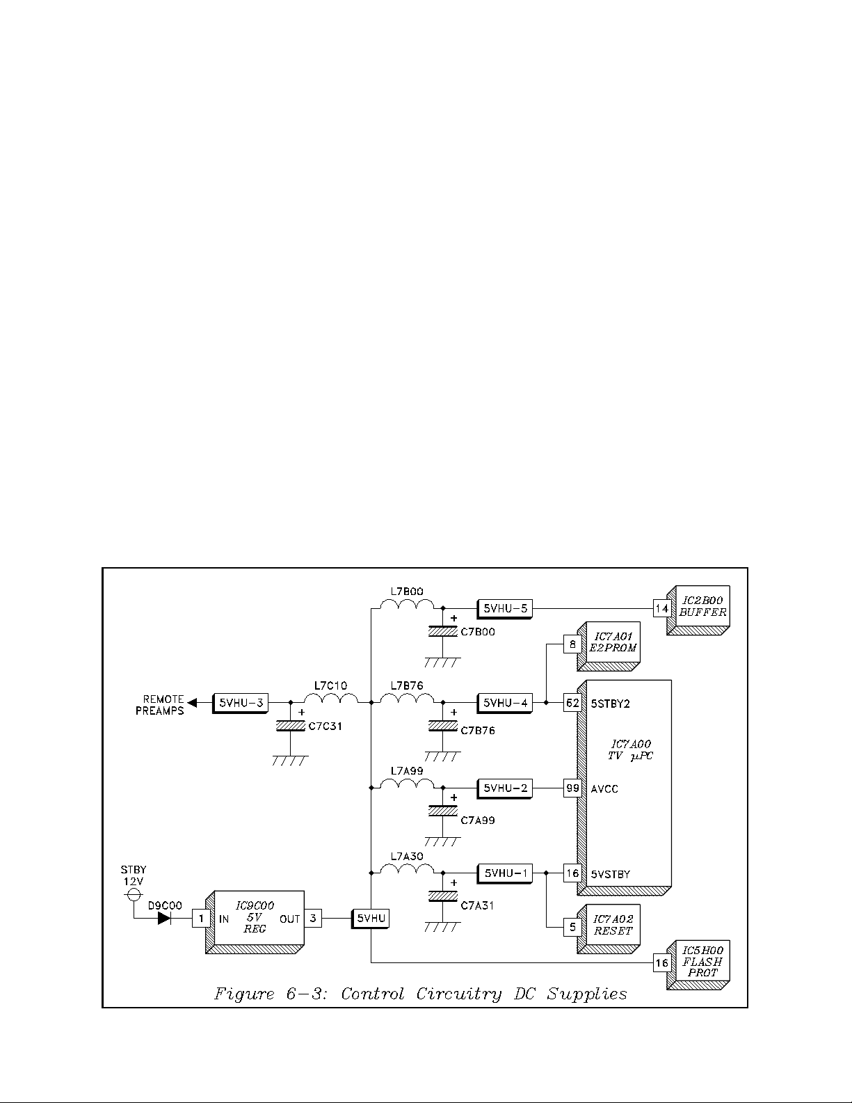
Figure 6-3 shows the DC supplies for the TV µPC circuitry. The TV µPC requires a 5 volt DC supply. The
STBY 12V supply is the source for the Control circuitry 5 volt supplies. IC9C00 regulates the 12 volts
down to 5 volts, the 5VHU DC supply.
The 5VHU supplies power directly to IC5H00, the
Flash Protect IC, and is the source for all the other
Control circuitry 5 Volt supplies. Each of the supplies is isolated by Low Pass LC Filters.
• 5VHU-1 … Supplies IC7A00 5V STBY and
Reset IC, IC7A02
• 5VHU-2 … Supplies IC7A00 AVCC
• 5VHU-3 … Supplies the Remote Preamps
• 5VHU-4 … IC7A00 5V STBY2 and
E2PROM IC, IC7A01
• 5VHU-5 … Supplies Buffer IC, IC2B00
Reset Circuitry
Microprocessors must be reset to their nominal state
when power is first applied, otherwise lockup occurs. Figure 6-4 shows the Reset circuitry in the
V19. The TV µPC’s Reset Input is at pin 12. Reset
6-4
Page 35

IC, IC7A02, generates a delayed reset pulse when
power is applied.
IC7A02 is a Reset Watchdog type of IC. When the
µPC is functioning, pulses are output at pin 73 of
IC7A00. The pulses constantly reset the counter in
IC7A02 and no Reset pulse is generated.
If lock up occurs, no pulses are generated at pin 73.
With no pulses from the TV µPC the counter in
IC7A02 is not reset and a Reset pulse is generated.
The same type of Reset action resets in the DM µPC
circuit.
If communication is
lost from either the
TV µPC or from the
DM µPC, the other
µPC automatically
generates a Reset
pulse. A Low at pin
11 of IC7A00 resets
the DM µPC, and a
Low from pin 10 of
the DB connector resets the TV µPC.
Both Reset commands are routed through IC7B80, that
functions basically as an AND gate. This enables the
front panel Manual Reset button to Reset both µPCs.
V-CHIP Blocking Circuitry
The V-Chip Blocking circuitry allows blocking of
specific type of programming. Program rating information is located on line 21 of the TV signal. The
circuit configurations is not new but is presented here
as a reference.
6-5
Page 36

Figure 6-5 shows the V-Chip Blocking circuitry in the
V19. Main picture V-Chip circuitry is in the TV µPC.
Main picture Y signal is input to IC7A00 at pin 100.
The current program rating is read and if necessary the
µPC blocks the program.
The AC signal applied to Bridge Rectifier D9A01 is
monitored. D9A01 is the DC source for both Standby
and Switched Regulators. The AC source is connected to the inputs of the Bridge Rectifier, and the
circuit is reference to a Hot ground.
IC7V01 is used to monitor the rating of the sub picture signal. Sub picture video is input to IC7V01 at
pin 7. The internal circuitry reads the program rating data on line 21 and sends it to the TV µPC over
the Program Block line. If that particular program
rating has been blocked the µPC blocks the sub picture in the 2HDW circuitry. When the sub picture is
blocked, the PIP/POP insert is black.
AC-OFF Circuit
The AC-OFF circuit is not new. When a logic change
at the AC-OFF input of the TV µPC indicates an AC
power loss, the Control circuitry rapidly stores all
user programming and service adjustments in memory
before the DC supplies drop to zero.
Although the purpose of the circuitry has not
changed, the method of monitoring the AC source is
different in the V19. Figure 6-6 illustrates the AC-
OFF monitoring circuit in the V19.
The signals at the rectifier inputs, in reference to the
Hot ground, are AC sine waves 180 degrees out of
phase. Both signals are resistive coupled to the base
of Q9A54. Diode D9A28 removes the negative half
of each signal. The resulting positive half cycles of
each sine wave keep the transistor conducting.
With Q9A54 On, the LED and Photo Transistor in
PC9A21 conduct, holding Q7B90 On. This holds
the AC-OFF input of IC7A00 Low. If an AC power
loss occurs, Q9A54, PC9A21 and Q7B90 stop conduction. This allows pin 20 of IC7A00 to go High,
indicating AC power has been lost.
When this occurs, the TV µPC outputs a momentary High at pin 82, which is directed to the DM
Module. This is the Power Good line, informing the
DM Control circuitry of the power loss.
6-6
Page 37

Name Pin No. Purpose
AFT1 92 Main Tuner Tuning
AFT2 93 Sub Tuner Tuning
AC-OFF 20 Loss of AC Power
H-SYNC 97 Horizontal Sync
DM-DET 26 DM connected
SD1 7 Main Tuner Signal Present
SD2 6 Sub Tuner Signal Present
SHORT 46 Power Supply Short
V-BLANK 94 Video is blanked
VSYNC 95 Vertical Sync
XRAY 47 Shuts the TV Off
Table 6-1: TV µPC Inputs
Name Pin No. Description
ANT-A 81 Select Ant-A or Ant-B
BLANK-CRT 2 Blanks CRT through CRT Protect Circuitry
DVD-SW 53 Selects DVD-1 or DVD-2
IR-IN-BUSY 43 IR Signal to DM for System 5
LED 4 Front Panel Led Control
M-FRUN 83 Main Picture Freerun
MN-SYNC-SW 24 Main Picture Sync Switch Control
MUTE-MON 86 Mutes sound from Monitor Outputs
MUTE-SPKR 80 Mutes sound from the set's speakers
MUTE-SUB 87 Mutes sound from the Sub Monitor Outputs
NT-SW 51 Selects NTSC Y signal source
PON-1 50 Power ON command
PON-2 49 Power On command (signal processing circuits)
POWER GOOD 82 High = AC Power Loss
S-FRUN 84 Sub Picture Freerun
SUB-CONTRAST 25 Reduces video amplitude during Sub Contrast Adjust.
SUB-SYNC-SW 23 Sub Picture Sync Switch Control
Table 6-2: TV uPC Outputs
Additional Inputs and Outputs
There of course specific purpose inputs and output on
the TV µPC. Most of the inputs are status inputs and
the outputs are specific commands. The specific purpose inputs are listed in Table 6-1, and the outputs in
Table 6-2.
In the V19/V21 the Short input at pin 46 of the µPC
only monitors the positive and negative 24 Volt supplies. The Power Good output at pin 82 is normally
Low. If AC is lost, pin 82 goes High.
DM Module Control Circuitry
Since the DM Module is considered a replaceable component, an in depth circuit description is not required.
Only a simplified overall view is needed.
Figure 6-7 shows a Simplified Overall Block Diagram of the Control Circuitry in the DM Module.
The heart of the Control Circuitry is the DM µPC.
The E2PROM, on the E2P Module, stores most of
the user and service adjustment data.
6-7
Page 38

The DM µPC communicates with the TV µPC through
the System Interface and UART (Universal Asynchronous Receiver Transmitter) circuitry. Data from the TV
µPC is received over the TV DM TXD line, and data is
sent to the TV µPC over the TV DM RXD line. The
TV DM CTS and TV DM RTS are Clear to Transmit
and Request to Transmit, respectively. They are used
to provide slow control on RXD and TXD lines.
The DM µPC, through the System Interface, controls the:
• ATSC/QAM Tuner/Demodulator
• MPEG Decoder
• OSD Generator
• IR µPC
The ATSC/QAM Tuner receives and processes Digital HD, SD and QAM (digital cable) Signals. The
output is the Transport Data Stream, directed to the
MPEG Decoder through the System Interface.
All On Screen Display (OSD) signals, except Convergence OSD, are generated in the DM OSD circuit.
When the main picture source is digital, from the ATV
Tuner or 1394 Jacks, the OSD is inserted in the DM
Module.
When the main picture source is analog, the OSD
signals are output from the MPEG circuit and inserted in the main picture in the VCJ IC.
The IR µPC receives remote signals from the TV
µPC over the IR IN/BUSY line. The signals are
decoded and directed to the System 5 IR Outputs
for controlling Home Theater components.
It was previously mentioned that the 1394 Jacks were
the source of Digital Signals. When digital components in a Home Theater setup are IEEE 1394 compatible, a single four lead cable connection is all that
is required.
The MPEG Decoder processes the Transport Data
Stream and outputs analog RGB signals.
Two of the IEEE 1394 cable leads are data lines, and
two are control lines. The IEEE 1394 system en-
6-8
Page 39
ables digital data stream transfer between 1394 units in
the Home Theater setup.
There is one additional external connection shown
in Figure 6-7, a Compact Flash Memory Card Slot.
This enables soft ware updates in the field, if required.
Software Update
If and when software updates are required they can
be performed by technicians in the field. Software
updates will be on a plug in Compact Flash Card,
available from the Parts Department.
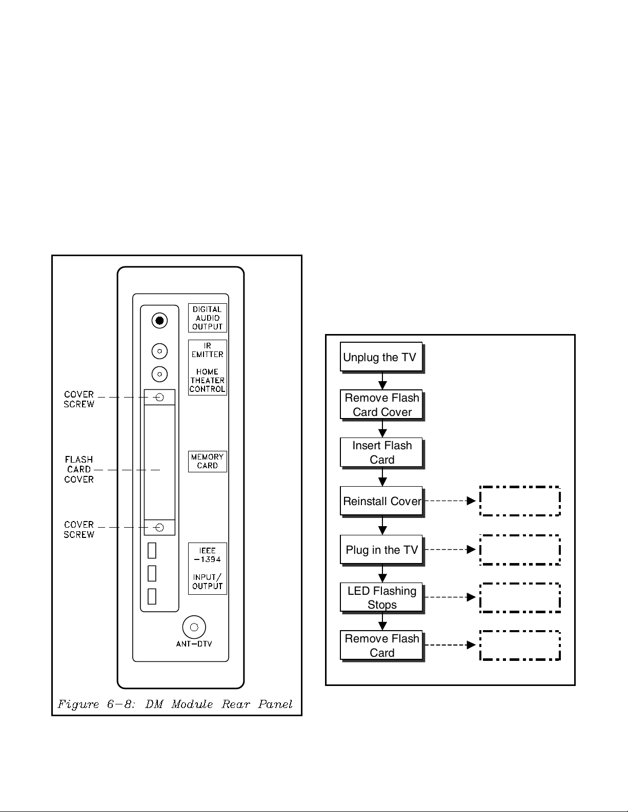
Figure 6-8 shows the DM Module Rear Panel. To
access the Flash Card slot, remove the Flash Card
Cover by removing the mounting screws. This exposes the slot for the Flash Card and a Blue button.
During the update, the Blue button must be depressed. After inserting the Flash Card, reinstalling
the cover will hold the button depressed.
Figure 6-9 shows the basic Software Update Procedure in flow chart form. During the update, the front
panel LED flashes. When the LED stops flashing,
the update is complete.
Unplug the TV
Remove Flash
Card Cover
Insert Flash
Card
Reinstall Cover
Plug in the TV
LED Flashing
Stops
Remove Flash
Card
Holds Blue
Button In
LED Flashes
(4 minutes)
Update
Complete
Canbereused
Figure 6-9: Software Update Procedure
6-9
Page 40

E2P MODULE
Figure 6-10: E2P Module Location
DM Module Replacement
Most user and service adjustment data is stored on the
internal E2P Module. Before installing a replacement
DM Module. Remove the cover on both the old and
new modules.
Important: Unplug the E2P Module from both DM
Modules. Insert the old E2P Module into the new
replacement DM Module. Refer to Figure 6-10 for
the general location of the E2P Module Figure 6-11
shows a close up of the E2P Module plugged in.
Figure 6-12 shows the E2P Module unplugged.
Installing the E2P Module in the new DM Module
insures only minimal adjustment is required after installing the replacement DM Module.
6-10
Page 41

E2P MODULE
Figure 6-11: E2P Module Plugged In
Figure 6-12: E2P Module Unplugged
6-11
Page 42

6-12
Page 43
Chapter 7
Video/Color Circuitry
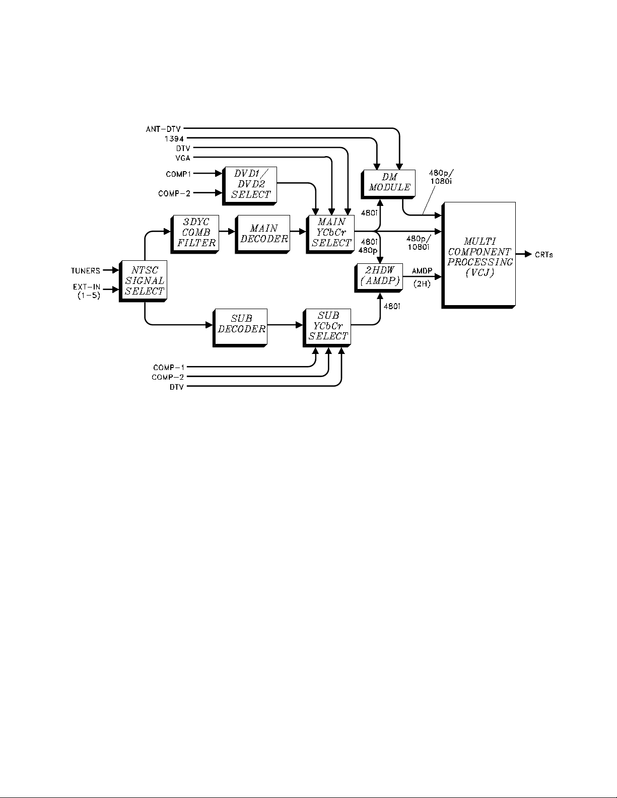
The above Simplified Block Diagram represents the
Video/Color circuitry in the V19/V21 chassis. The analog section of the circuitry is similar to that in the V17
and V18 chassis.
• NTSC Signal Select – Selects the Main and
Sub Picture NTSC signal sources.
• 3DYC Comb Filter – Separates the luminance (Y) and chroma (C) signals when the
main source is NTSC composite video.
• Main and Sub Decoders – convert their
respective signals to the component format
(YCbCr).
• YCbCr Select circuitry – selects the YCbCr
main and sub picture signals.
• 2HDW (AMDP) circuitry – performs line
doubling, PIP/POP and display format signal
processing..
• Multi Component Processor (VCJ) – processes the YCbCr signals and converts them
to the RGB format to drive the CRTs.
Only 480i signals are valid sources for PIP/POP signal
processing in the 2HDW circuitry. Therefore the PIP/
POP features are only possible when both the main and
sub picture signals are 480i format. 480p signals are
only processed in the 2HDW circuit when a display format change is selected.
Main picture 480p (with no display format change)
and 1080i signals are applied directly to the VCJ,
bypassing the 2HDW circuit.
The biggest change in the V19/V21 Video/Color circuitry is the addition of a DM Module. The circuitry in
the DM Module consists of:
• ATV/QAM Tuner and Demodulator.
• HD MPEG2 Decoder
• IEEE-1394 Interface
This enables the V19/V21 to receive and decode High
Definition broadcasts, and Digital Cable signals (when
not scrambled), without using a Set Top Box. The IEEE1394 interface enables single cable connection to 1394
compatible Digital Devices in a Home Theater System.
7-1
Page 44

NTSC Signal Selection
Figure 7-1 illustrates the NTSC Signal Selection circuitry. The circuitry is basically the same as in the V17
chassis. However, some pin numbers and nomenclature are different, due mainly to the addition of another
NTSC External Input.
IC2L00 selects main and sub picture NTSC signal from
the External 1, 3, 4 and 5 Inputs. External 5 inputs are
the front panel inputs.
IC2K00 selects main and sub picture signals from
IC2L00, or from the External 2 input, Main Tuner or
Sub Tuner. The selected main picture signals are directed to 3DYC Comb Filter circuitry, and sub picture
video is directed to the Sub Decoder.
The COMP-1, COMP-2, DTV and VGA inputs are
directed to YCbCr Select circuitry on the PCB-SIGNAL. Since a Set Top Box is not required to receive
HD broadcasts, the DTV inputs are mainly used for
connection to a Digital Broadcast Satellite (DBS).
7-2
Page 45

PCB-SIGNAL Video/Color Path
Main Picture Signal Path
Figure 7-2 shows the Overall Video/Color Signal
Path on the PCB-SIGNAL. NTSC main picture signal from the A/V SW circuitry is routed through PCBSIGNAL to PCB-3DYC.
The Comb Filter on the PCB-3DYC separates the Y
and C signals, and the Main Decoder converts the Y
and C signals to YCbCr. The signals are then directed to YCbCr Select circuitry on the PCB-SIGNAL.
The Main YCbCr Select circuit selects signals from
the Main Decoder, or the Component, DTV or the
VGA inputs. The selected signals can be:
• 480i – YCbCr are directed to PCB-2HDW
and CbCr to the DM Module. The 480i Y
signal, directly from PCB-3DYC, is routed
to the DM Module.
• 480p – YCbCr are directed to the VCJ and
2HDW. 2HDW circuitry only processes
480p when there is a display format change.
• 1080i – YCbCr are directed to the VCJ
The 480i Y signal for both the DM Module and the
Monitor Outputs must include sync signals. Since
the Main Decoder strips sync from the Y signal, it
must be directed to the DM and Monitor Outputs
before Main Decoder processing.
The PCB-2HDW doubles the number of horizontal lines
in 480i signals. The output signals from 2HDW, Y-
7-3
Page 46

AMDP, Cb-AMDP and Cr-AMDP are directed to the
VCJ.
When the main picture source is a HD Broadcast or
QAM cable signal, the circuitry in the DM Module
processes the signals and outputs the resulting analog RGB signals. The DM RGB signals are applied
to two sets of inputs on the VCJ:
1) DM Main Picture Input
2) OSD Insertion Input
All on screen (OSD) display signals are generated in
the DM Module, except Convergence OSD. When
the main picture source is digital, HD or QAM, OSD
insertion occurs in the DM Module. When the main
picture is an analog signal, RGB OSD signals from
the DM Module are directed to the OSD insertion
inputs on the VCJ and are inserted in the main picture in the VCJ.
The VCJ processes the selected signals, and converts
them to the RGB format to drive the CRTs.
Sub Picture Signal Path
Sub picture NTSC signals, from the A/V Switch circuitry, are converted to YCbCr signals by the Sub
Decoder. The output from the Sub Decoder is applied
to the Sub YCbCr Select circuit. Signals from the
COMP-1, COMP-2 and DTV inputs are also directed
to the Sub YCbCr Select circuit.
The selected signals are directed to 2HDW circuitry
for PIP/POP processing, and insertion into the main
picture. The sub picture source must be 480i or it is
not accepted by the 2HDW circuitry.
3DYC and Main Decoder Circuitry
Figure 7-3 illustrates the circuitry on the PCB-3DYC.
This circuitry is also basically the same as in the V17
and V18 chassis. When the main picture source is
NTSC composite video:
• The video signal is input to IC2C00 at pin 88
for Y and C signal separation.
• Y signal is output at pin 84 of IC2C00 and
directed to the NTSC SW, IC2Y01.
• C signal is output at pin 83 and applied to
the Main Decoder, IC2E00.
When the main signal is S-Y/C:
• The C signal still passes through IC2C00 for
noise reduction.
7-4
Page 47

• The Y signal is applied to the NTSC SW,
IC2Y01.
The NTSC SW selects the S-Y signal, or the Y signal from IC2C00. The selected Y signal is applied
to the Main Decoder.
IC2A00 is a new IC (Generic #CXA2151Q). It selects the main picture YCbCr signals from:
• The output of IC2A60
• The output of the Main Decoder
• The DTV Inputs
• The VGA Input
The Main Decoder converts the Y and C signal to
YCbCr and directs them to Main YCbCr Select circuitry on the PCB-SIGNAL.
Note that Y signal at the input to the Main Decoder
is also directed to the DM Module and the Monitor
Outputs.
YCbCr Select Circuitry
Figure 7-4 shows the Main Picture YCbCr Select
Circuitry. Compared to that in the V17 and V18,
the circuitry has been simplified. The DVD Select
IC, IC2A60, selects either COMP-1 or COMP-2 signal.
The path of the selected signals from IC2A00 depends on the signals format:
• 480i and 480p YCbCr signals are directed to
2HDW, and CbCr to the DM Module
circuitry. Y signal for the DM comes directly from PCB-3DYC.
• 480p and 1080i YCbCr signals are directed
to the Bypass Inputs on the VCJ.
The selected output from IC2A00 is always in the
component format (YCbCr). If the selected signals
are RGB, from the DTV or VGA inputs, they are
converted to YCbCr in IC2A00.
7-5
Page 48
Figure 5 illustrates the Sub Picture YCbCr Select
Circuitry. Sub picture NTSC signal is converted to
the YCbCr format in the Sub Decoder, IC2H00. The
output of IC2H00 is applied to IC2B00. Signals from
the COMP-1, COMP-2 and DTV Inputs are also
applied to IC2B00.
The outputs of IC2B00 are directed to the sub picture inputs of the 2HDW circuitry. If the format is
not 480i that signal will not be accepted by the 2HDW
circuitry.
YCbCr Select Control
Both the Main YCbCr Select (IC2A00) and Sub
YCbCr Select (IC2B00) are Controlled by the SDAMN data line. The SCL-MN clock line provides timing for data transfer. The internal circuitry of the
ICs detects the format of the selected signals and informs the TV Control µPC of that format, via the SDAMN I2C Data line.
VCJ Video/Color Signal Path
Figure 7-6 shows the Video/Color Signal Path in the
VCJ, IC2V00. Main picture signal inputs are:
• Pins 67-69 … 480i line doubled inputs.
• Pins 3-5 … 480p and 1080i analog inputs.
• Pins 15-17 … DM RGB inputs.
DM-RGB signals are converted to YCbCr in the VCJ.
Internal Switch circuitry selects Analog 480p/1080i
or DM YCbCr, and outputs the signals at pins 76-
78. This signals are directed back to pins 73-75 of
the VCJ.
7-6
Page 49

Another internal switch in the VCJ selects the signals at
pins 67-69 or pins 73-75 and directs the signals to the
internal YCbCr Processing circuitry. The signals are
converted to RGB and are directed to RGB Processing
circuitry. The RGB signals are output at pins 35, 37
and 39, and directed to the CRT Drive circuitry.
DM-RGB conversion to YCbCr enables using the
enhancements available in the YCbCr Signal Processing circuitry of the VCJ. For instance, the generation of a drive signal for the Scan Velocity Modulation (SVM) circuitry.
Note that the DM RGB signals are also input to the
VCJ at pin 49-51. These inputs are used for OSD
insertion when the main picture source is analog. The
DM-BLK signal, from the DM Module, times the
OSD insertion into the main picture.
When the main picture source is from the DM Module, the OSD is inserted in the main picture in the
DM Module.
Pins 45-47 are also OSD Inputs. These inputs receive OSD signals from the Convergence circuitry,
and the CBLK signal times the Convergence OSD
insertion.
7-7
Page 50

CRT Drive & Protect Circuitry
Figure 7-7 illustrates the CRT Drive and CRT Protect
circuitry. The CRT Drive circuitry is the same as that in
the V17, except that the three discrete component transistor amplifiers on each PCB-CRT are replaced with a
single IC, IC6B01, IC6G01 or IC6R01. Only the PCBCRT(B) is shown in Figure 7-7.
Transistors Q2W05, Q2W08 and Q2W11 are part
of the CRT Protect circuitry. When these transistors
conduct it removes the drive to the CRTs. Q2W03
controls the conduction of all three of CRT Protect
transistors.
The conduction of Q2W03 is controlled by the
VBLNK and BLANK CRT lines. The BLANK-CRT
line momentarily goes Low during a channel or input
change, momentarily blanking the CRTs.
The VBLNK line goes High if deflection is lost. The
High turn Q2W03 On, blanking all three CRTs to
prevent possible CRT phosphor damage.
In the V17 Spot Killer circuitry was also part of the
CRT Protect circuitry. This circuit has been replaced
by Flash Protect circuitry. The Flash Protect circuit
and Deflection Detection Loss circuitry are described
in Chapter 8.
Monitor Out Signal Path
The Video/Color Monitor Signal Path is shown in Figure 7-8. NTSC signal for the Monitor Outputs is de-
rived from the C output of the 3DYC Comb Filter, and
7-8
Page 51

the Y output of the NTSC SW, IC2Y01. The two signals are applied to A/V-SW, IC2L00, and forwarded
to the Main Inputs on IC2K00.
When the main signal source is composite video, there
would be no Y and C signal input to IC2K00's main
inputs. These signals are supplied by the Y and C
signals from PCB-3DYC. The signals at pins 1, 3,
and 5 of IC2K00 are output at pins 37, 39 and 41,
and directed to the Monitor Output Jacks.
When the main signal source is HD or SD from the DM
Module. The circuitry in the DM Module outputs analog Y-DM and C-DM signals which are directed to
IC2K00. Internal to IC2K00 the Y and C signals are
combined to form a Composite Video signal. All three
signals V-DM, Y-DM and C-DM are directed to the
Monitor Output Jacks.
If any other source, Component, DTV or VGA is
the main picture source, no signal is available at the
Monitor Outputs.
7-9
Page 52

DM Basic Signal Block
Figure 7-9 shows a Basic Block Diagram of the Signal
Processing circuitry in the DM Module. Only a simple
Block Diagram is necessary since the DM Module is a
replaceable component.
of the Demodulator is the HD Transport Data Stream.
It is directed through the System Interface circuitry
to an MPEG Decoder. The Decoder outputs main
picture analog RGB, and also Separate Y and C signals for the Monitor Output circuitry.
There are two main signal sources for the DM Module:
1) ANT-DTV Input
2) 1394 Jacks.
Signals from ANT-DTV input are processed by the
ATV Tuner and Demodulation circuitry. The output
The other signal sources for the DM Module are the
1394 Jacks. The signal input to the 1394 Jack would
be a compressed digital data stream from a 1394
Compatible Digital Device in a Home Theater System. This signal is routed through the System Interface circuitry to the MPEG Decoder. The output of
the Decoder is main picture analog RGB.
7-10
Page 53

Chapter 8
Deflection & HV Circuitry
Although some nomenclature differs, the Deflection
circuitry is mostly the same as in previous models.
The main changes are:
• The Sync Signal Path differs.
• An added Flash Protect circuit.
Sync Block Diagram
The above Block Diagram shows the Sync Signal
path from the source to the VCJ, which generates
drive for the Vertical and Horizontal Deflection circuitry.
The sync source for NTSC signals, and component
format signals is in the Y or composite video (NTSC)
signal. The A/V Switch circuitry selects the Y, or
video signal of the desired source.
The output of the A/V Switch takes two paths:
1) To the Main Decoder
2) To a Sync Separator circuit.
The Main Decoder outputs separated Horizontal and
Vertical Sync. The Sync Separator outputs composite
sync (CSYNC), combined horizontal and vertical.
The CSYNC signal is applied, to the Main YCbCr
Select circuitry. Horizontal and Vertical Sync from
the DTV and VGA inputs are also directed to the
YCbCr Select circuit.
The CSYNC signal is broken down to separate horizontal and vertical sync, and when selected as the
signal source is output from the YCbCr Select circuit. Horizontal and vertical sync from the YCbCr
Select circuit is applied to one set of inputs on a Sync
Select IC.
The second set of inputs to the Sync Select IC receives sync from the Main Decoder. The difference
in the two sets of sync signals is NTSC Sync from
the YCbCr Select circuit contains equalizing pulses.
The signals from the Main Decoder are generated by
count down circuitry and have no equalizing pulses.
8-1
Page 54

The 2HDW circuitry requires sync with no equalizing pulses. Therefore when the source signal is 480i,
the sync from the Main Decoder is selected and directed to the 2HDW circuitry.
When the source signal is 480i the horizontal lines
are doubled in the 2HDW circuitry and the resulting
2H signal is directed to the VCJ. When the source is
480p, the sync signals from the Sync Select IC are
applied directly to the VCJ.
An additional sync source in the V19 is from DM
Module. When receiving a digital broadcast or digi-
tal cable signal, the signal is decoded in the DM Module and DM horizontal and vertical sync are directed
to the VCJ.
The VCJ selects 2H sync from 2HDW, analog 480p/
1080i sync, or the 480p/1080i sync from the DM
Module. The selected sync is processed, output from
the VCJ and directed to the Deflection Generators
on PCB-JUNGLE.
Figure 8-1 shows the Sync Signal path in more detail, showing ICs, pin numbers and connectors in the
Sync Path.
8-2
Page 55

Deflection and HV Circuitry
Figure 8-2 illustrates the Deflection and High Voltage circuitry. Horizontal and Vertical Sync signals
from the VCJ are routed from the PCB-SIGNAL,
through PCB-POWER and PCB-MAIN to the Deflection Jungle IC on PCB-JUNGLE.
Vertical sync is applied directly to pin 2 of IC4A01.
Horizontal sync triggers a MMV in IC4A03. The
clean output pulse from the MMV is applied to pin
32 of IC4A01. The horizontal and vertical Deflection Drive signals from IC4A01 are directed to the
Deflection circuitry on PCB-MAIN.
Vertical Drive is applied to IC4B01, the Vertical
Output IC, amplified and directed to the Vertical Yoke
Coils through the DY connector.
Horizontal Drive is amplified by Q5A33 and Q5A32
and applied to the base of Q5A31, the Horizontal
Output transistor. The output of Q5A31 takes three
paths.
1) To Horizontal Deflection Yoke coils.
2) Through T5A31 to generate the CRT filament supply.
3) Through C5A34 to the HV circuitry.
Q5A01 regulates the DC supply for Q5A31 and also
is the source for horizontal pincushion correction.
The HV Drive passes through Q5A37, the HV Regulation IC (IC5A00), and Q5A51 to drive the Flyback
Transformer. Note that the DC Supply for IC5A00
is denoted as HV 12V. This supply is generated specifically for the HV Drive circuitry.
8-3
Page 56

HV 12 Volt Supply
Figure 8-3 shows the HV 12V supply circuitry. The
source of the supply is the 24 Supply from the Main
Power Supply, applied to the collector of Q5A08. A
10 volt reference, from IC5A03 is applied to the inverting input of an Op-amp in IC5A01. A sample of
the voltage at the emitter of Q5A08 is applied to the
non-inverting input.
The output of the Op-amp controls the conduction
of Q5A08. Conduction increases if the voltage at
the emitter drops below 12 volts, and decreases if
the voltage exceeds 12 volts. The HV 12V supply is
routed through a jumper in the DK connector to
IC5A00.
The DK connector is connected to the ground returns of the HV Block. If the set is operational with
the DK connector unplugged, excessive HV would
be generated causing damage to the TV. The jumper
in the DK connector insures that the HV is disabled
when the connector is unplugged.
8-4
Page 57

HV Regulation
The HV Regulation circuitry is shown in Figure 8-4.
Controlling the duty cycle of the drive applied to the
HV Output transistor, Q5A51, regulates the HV. The
amount of energy stored in the Flyback transformer
is determined by how long Q5A51 conducts. Increasing conduction time increases HV, and decreasing conduction time reduces HV.
A sample of the HV is derived from the HV Block
ground return circuitry. DC feedback (HV FB DC)
is directed through an Op-amp in IC5A01 to the HVIN input at pin 6 of IC5A00. AC feedback (HV FB
AC) is applied directly to pin 6 to speed up the operation.
in excessive HV. HV FB DC can safely be measured
after buffering by the Op-amp in IC5A01.
The sample of the HV is compared to the HV-ADJ
voltage from the Convergence circuitry, input at pin
11 of IC5A00. If the HV feedback voltage is higher
than the HV-ADJ voltage, conduction time is decreased. Conversely, if the feedback voltage is lower,
conduction time is increased.
X-Ray Protect
Figure 8-5 illustrates the X-Ray Protect circuitry. It
is the same as in the V17 and V18 chassis. The XRay Protect circuitry shuts the TV down if High
Voltage, Beam Current or arcing is excessive.
Caution: Do not measure HV FB DC at the DK
connector. This will load down the circuit resulting
D5A57 provides a sample of the HV by rectifying
the signal from pin 5 of the Flyback. Beam current is
detected by monitoring the voltage at the ground
return for the HV winding
in the Flyback, pin 8 of
T5A51.
The voltage from D5A57 is
applied to the (-) input of
an Op-amp in IC5A02.
Reference IC5A03 hold the
(+) input at 10 volts. If the
voltage for D5A57 exceeds
the 10 volt reference, the
output of the Op-amp goes
Low, pulling the X-Ray line
Low. The TV µPC responds by turning the TV
Off.
A similar Op-amp configuration monitors beam current. Pin 8 of the Flyback
is connected through
D5A59 to the (+) input (pin
5) of another OP-amp in
IC5A02. The (-) input (pin
6) is a reference voltage
derived from R5A66,
R5A67 and the 12V supply.
8-5
Page 58

As beam current increases, the
voltage at pin 8 of the Flyback
decreases. When the voltage
at pin 5 of IC5A02 drops below the reference at pin 6, the
output at pin 7 goes Low, shutting the set Off.
Other circuitry in IC5A00 provides additional protection.
By monitoring the voltage
across R5A51 at pin 7 of
IC5A00, the HV Output transistor current is sensed. If the
voltage becomes excessive,
IC5A00 removes drive to
Q5A51.
Pin 10 of IC5A00 is used to
remove HV drive if a sudden
arc occurs. Q5A06 normally
does not conduct. If an arc
occurs, the voltage at pin 8 of
the Flyback drops suddenly:
• Exceeding the zener
point of D5A60.
• Turning Q5A06 On
• The resulting High at
pin 10 of IC5A00
removes HV drive.
Deflection Loss Detection
In the chapter on Video/Color, the CRT Protection
Circuit was described. This circuit cuts off all three
CRTs to prevent phosphor damage due to loss of
deflection. Figure 8-6 shows the Deflection Loss
Detection circuitry.
Q5A38 monitors horizontal deflection. Pulses from
the collector circuit of Q5A31 continually drives
Q5A38 into conduction. The average collector voltage is below the turn on point of D5A12. If horizontal deflection is lost:
• Q5A38 shuts Off
• Q5A38 collector voltage rises.
• D5A12 is forward biased
• VBLNK goes High, activating CRT Protect.
Q4B01 monitors vertical deflection. The vertical
sawtooth from the Vertical Yokes ground return
drives Q4B01 into conduction. If vertical deflection is lost:
• Q4B01 stops conducting.
• Q4B01 collector voltage rises
• D5A13 is forward biased.
• VBLNK goes High.
Since the 24V supply is the source of the HV 12V
supply, the 24V supply is monitored for further
protection. Q5A07 does not normally conduct. If
the 24V supply is lost:
• The emitter of Q5A07 momentarily remains
High, due to the charge on C5A12.
8-6
Page 59
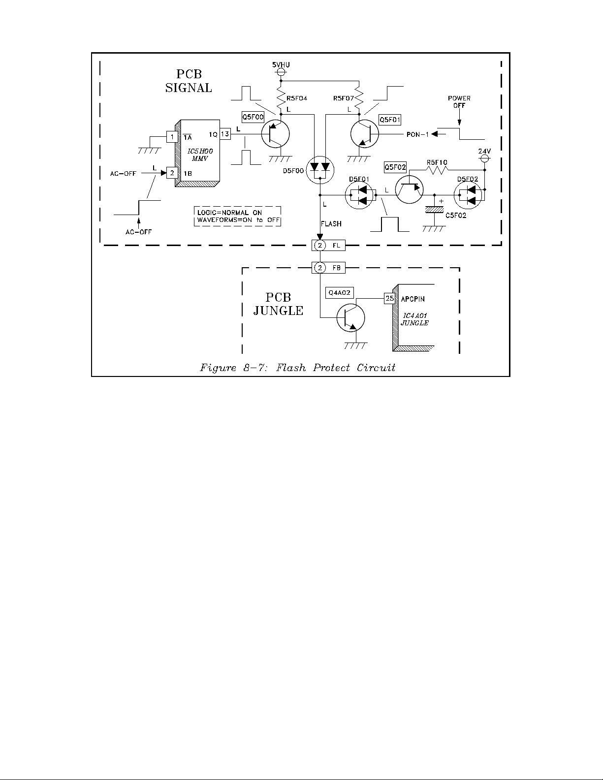
• Q5A07 conducts
• VBLNK goes High, activating CRT Protect
• Q4A02 conducts pulling pin 25 of the Jungle
IC Low.
• HV is removed.
Flash Protect Circuit
The Flash Protect circuit in Figure 8-7 is new. It
prevents the screen from flashing by removing HV:
• If AC Power is lost.
• When switching Power from On to Off
• If the 24V supply is lost.
IC5H00 is a one shot multivibrator and monitors the
AC-OFF line. When power is lost:
• The AC-OFF line momentarily goes High.
• IC5H00 is triggered an outputs a positive
pulse.
This same action occurs when Power is switched from
On to Off.
• The P-ON1 line goes Low.
• Q5F01 stops conduction.
• Q5F01 collector voltage rises.
• Q4A02 conducts removing HV.
Loss of the 24V supply has the same effect.
• Q5F02 momentarily conducts due to the
charge on C5F02.
• Q4A02 conducts.
• HV is removed.
8-7
Page 60

8-8
Page 61

Chapter 9
Sound Circuitry
Like most of the analog circuitry in the V19/V21, the
Sound Circuitry is almost identical to previous models.
This is apparent from the above Simplified Block Diagram.
The Sound Source Select circuitry selects the sound
source for both the main and sub pictures. Most of
the sources are conventional and have been available in the past:
• Main Tuner
• Sub Tuner (monaural only)
• Five External NTSC Inputs
• Two Component Inputs (DVD)
One additional sound source is added in the V19/V21
chassis, DM-R and DM-L. This is the sound signal
from the DM Module. It is initially received in a
digital format, from the ATSC/QAM Tuner or the
IEEE 1394 inputs. The DM-R and DM-L signal are
analog stereo signals that are directed to the Sound
Source Select circuitry.
The remainder of the circuitry is the same as in many
previous models:
• MCS Decoder circuitry decodes the Main
Tuner sound signal, generating mono, stereo,
or SAP signals when broadcast.
• Main picture sound from the Select circuitry
takes two paths:
1) To Audio Control circuitry
2) To the Monitor Outputs
• The Audio Control circuitry performs adjustments to the Volume, Treble, Bass, etc. The
outputs from Audio Control circuit are
directed to the Audio Amplifier, and then to
the set’s speakers.
• Sub picture (PIP) sound, from the Source
Select circuit is directed to the PIP Sound
Output Jacks.
9-1
Page 62

9-2
Page 63
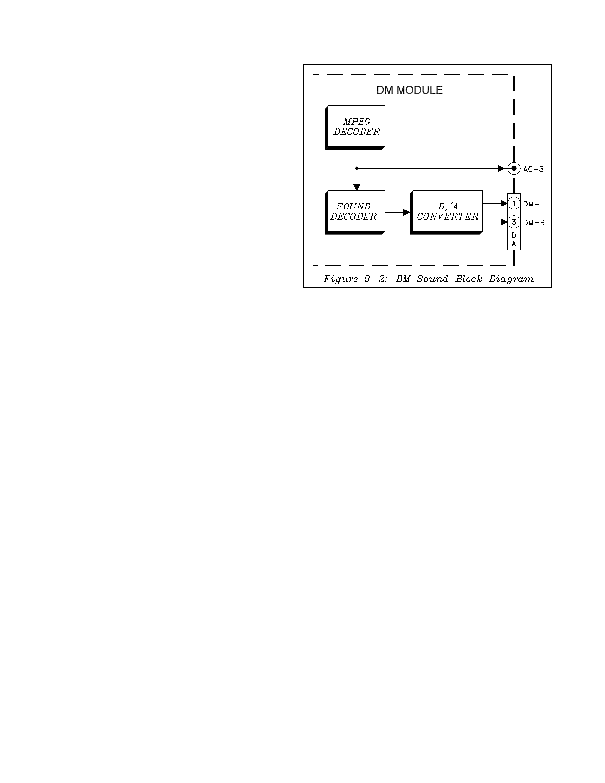
Overall Sound Signal Path
Figure 9-1 illustrates the Overall Sound Signal Path.
The AV/SW ICs, IC2L00 and IC2K00, used to select Main and Sub Picture Video/Color are used to
the select the Sound sources.
IC2L00 selects Main and Sub sound sources from
External NTSC Inputs 1, 3, 4, and 5, and from Component Inputs 1 and 2. The selected signals are directed to IC2K00.
IC2K00 selects the signals from IC2L00, or from
the Main Tuner, Sub Tuner, NTSC External Input 2,
DTV Inputs, or the DM Module. The Main Tuner
sound signal is decoded by MCS circuitry in IC3A01
before being applied to IC2K00.
The Sub (PIP) sound signal is routed from IC2K00
to the PIP Sound Output Jacks. The selected main
Sound signal is directed to Audio Control circuitry,
also in IC3A01. The sound signal from IC3A01 is
amplified in IC3E01 and directed to the set’s speak-
ers.
The input signals to IC3A01 are also directed to the
Monitor Output Jacks. Only fixed level sound is
available at the Monitor Output Jacks.
AC-3® Output
There is one additional sound output signal in the V19/
V21 chassis, External AC-3® Decoder Output on the
rear of DM Module. This is an AC-3® digital data stream
(when available from a digital source). It allows connection to external components with an AC-3® Decoder
AC-3® Decoder can produce 5.1 channel surround
sound, 5 full audio channels (20 kHz) and one low frequency enhancement channel (120 Hz).
Figure 9-2 shows a Basic Block Diagram of the
Sound circuitry in the DM Module.
9-3
Page 64

9-4
Page 65

Chapter 10
Convergence Circuitry
The Block Diagram above reveals the theory of operation of the Convergence Circuitry to be same as
in previous models. Horizontal and vertical pulses
are input to the Convergence Waveform Generator.
The Convergence Generator outputs six digital convergence correction signals:
• Red Horizontal Correction
• Green Horizontal Correction
• Blue Horizontal Correction
• Red Vertical Correction
• Green Vertical Correction
• Blue Vertical Correction
The digital correction signals are directed D/A Conversion circuitry and are converted to analog signals.
The signals then pass through LPF circuitry, removing any remaining high frequency digital signals. Then
the signals are amplified in Summing Amplifiers.
Green correction is added to the red and blue signals
at the inputs of the Summing Amplifiers.
The signals are then further amplified in Convergence
Output circuitry and directed to the Sub Coils in their
respective Deflection Yoke.
The Convergence Generator also develops the RGB
signal for the cross hatch pattern used during convergence alignments
Closer examination of the Convergence Circuitry will
show the main difference in the V19/V21 is fewer ICs
are used.
10-1
Page 66

Waveform Generator & A/D
Converter.
Figure 10-1 illustrates the Convergence Waveform
Generator and the A/D Converter. IC800 is the
Waveform Generator. It operates from a 3.3 volt
DC supply. No input buffers are needed for the horizontal and vertical pulses from the Deflection circuitry. Also the external PLL circuitry used in previous models is no longer required.
The same control signals from the Control circuitry
are used:
• C-SDA … I2C Data Line
• C-SCL …. I2C Clock Line
• C-ACK … Command Acknowledgment line
• C-BUSY … Busy Line
• C-MUTE … Momentarily disables the
Convergence Circuitry during Channel
Change, Input Change and during On/Off.
The HV-ADJ PWM signal and the DF parabolic signal are still generated in the Waveform Generator.
Six A/D Converter ICs were used in previous models.
In the V19/V21 there is only one A/D Converter IC,
10-2
Page 67

IC8E03. IC8E03 houses all the required A/D Converters.
LPF & Summing Amplifiers
The LPF and Summing Amplifier circuitry is shown in
Figure 10-2. Three ICs are used in the LPF and Summing Amplifier circuitry.
• IC804 … RH and GH LPF and Summing
Amplifier
• IC803 … BH and RV LPF and Summing
Amplifier
• IC802 … GV and BV LPF and Summing
Amplifier
10-3
Page 68
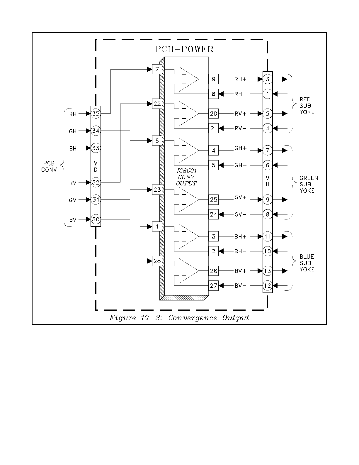
Note that Green Horizontal is added to Red and Blue
Horizontal second stage inputs, and Green Vertical
is added to the Red and Blue Vertical second stage
inputs.
The Green Correction voltage is used to correct green
raster distortion, but does effect the red and blue raster.
Therefore, green raster distortion must be adjusted first,
before adjusting red and blue convergence.
Convergence Output Circuitry
Figure 10-3 illustrates the Convergence Ouput circuitry.
In the V19, Convergence Output Circuitry is internal to
a single IC, IC8C01, located on the PCB-POWER. It
functions the same as in previous Output circuitry except only one IC is needed.
10-4
Page 69

Chapter 11
Troubleshooting Tips
LED Indications Conditions Probable Cause
Off After AC is applied Standy Power Supply or TV µPC not running
Fast Blink for 70 s ec. After AC is applied Normal - DM µPC is booting up
Fast Blink (doesn't stop) After A C is applied TV µPC is running, but DM failed to boot up
Slow Blink Set is Off Normal - Timer is set for Automatic Turn ON
Table 11-1: Front Panel LED Indications
Troubleshooting the analog circuitry in the V19/V21 is
basically the same as in previous modes. Although the
DM Module is a replaceable component, the service
technician must determine that it is the cause of a problem. The following tips are useful in determining the
source of a problem
Using The Front Panel LED
The Front Panel LED helps isolate the cause of the
following problems.
• The TV will not turn On.
• The TV turns On, and then Shuts Off.
If the TV will not turn On, the LED response indicates the possible cause of the problem. Table 11-1
lists the possible LED response when this problem
occurs.
When the TV turn On and then shuts Off, the LED
Diagnostic Error codes help isolate the problem. This
is the same LED Diagnostic featured on some previous model TVs.
Figure 11-1 shows the LED Error Code Activation
Procedure, an is describe in the following:
1) With the TV Off
2) Press and hold the front panel "MENU" and
"DEVICE" buttons for 5 seconds.
3) The LED will flash the Error Code indicating
what caused the TV to shut Off.
4) The Error Code will be repeated 5 times.
5) When the LED stops flashing the mode is
automatically terminated.
Reading the Error Codes
The Error Codes are two digit numbers. The LED:
• Flashes the value of the most significant digit
(MSD).
• Then there is a pause.
• Flashes the value of the least significant digit
(LSD).
• The Error Code is repeated 5 times.
11-1
Page 70

As an example, Figure 11-2 illustrates the LED drive
for Error Code "23". Table 11-2 lists the possible
Error Codes and there cause.
DM Module Check
When the TV turns On, but a problem exists that
may be caused by the DM Module, perform the following two checks:
1) Select the DTV Antenna as the source an
select and HD Channel.
2) Select an analog 480i signal as the source
and note if an On Screen Display (OSD) is
present.
The ability to receive an HD channel indicates the
DM Module is functioning properly.
Except for the convergence crosshatch, all OSD signals are generated in the DM Module. When there is
no OSD using a 480i source, the DM Module may
be the cause of the problem. However, before condemning the DM Module, make the following checks:
1) Check the VA connector, between the DM
Module and PCB-SIGNAL. If the VA
connector is disconnected, a 480i signal
picture will be generated but there is no
OSD.
2) Check for DSP-H and DSP-V signals at pins
10 and 11 of the VA connector.
Error Code Probable Cause
12 Normal Operation - No Error Detected
21 X-Ray Protect
22 Short Protect
23 Loss of Horizontal Deflection
24 Loss of Vertical Deflection
Table 11-2: Error Codes
If DSP-H and DSP-V are missing, check the analog
circuity. If they are present, the DM Module is probably at fault.
NetCommandTM Control Problems
If devices in a Home Theater System cannot be controlled properly with NetCommandTM, the Remote
Control may not be in the NetCommandTM Operational Mode. To put the Remote in the
NetCommandTM Mode:
1) Set the Remote to the TV Layer.
2) Point the Remote away from the TV.
3) Press and Hold the "POWER" button and
enter "9-3-5" in sequence.
CRT Phosphor Protection
Troubleshooting problems in the CRT Protect, Deflection Loss Detection and the Deflection circuits,
sometimes involves disabling the CRT Protect circuitry and then Powering up the TV.
However, first disable the CRTs to prevent any
possible phosphor damage.
1) Unplug the SP connector at the PCBCRT(R). This removes the filament voltage
to all three CRTs.
2) Remove zener diode D5A13 on PCB-MAIN.
This disables the CRT Protect circuit.
The set then can be switched on for troubleshooting
without damaging CRT phosphors.
11-2
Page 71

Copyright © 2002 Mitsubishi Digital Electronics America, Inc.
9351 Jeronimo Road • Irvine, CA 92618-1904
 Loading...