

MITSUBISHI RA30H4552M1 User Manual
< Silicon RF Power Modules >
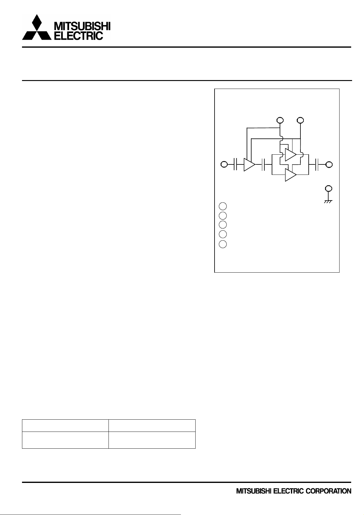
BLOCK
DIAGRAM
RA30H4552M1
RoHS Compliance, 450-520MHz 30W 12.5V, 2 Stage Amp. For MOBILE RADIO
DESCRIPTION
The RA30H4552M1 is a 30-watt RF MOSFET Amplifier Module for
12.5-volt mobile radios that operate in the 450- to 520-MHz range.
2
The battery can be connected directly to the drain of the
enhancement-mode MOSFET transistors. Without the gate
voltage (VGG=0V), only a small leakage current flows into the drain
and the nominal output signal (P
=30W) attenuates up to 60 dB.
out
The output power and the drain current increase as the gate
voltage increases. The output power and the drain current
1
increase substantially with the gate voltage around 0V(minimum).
The nominal output power becomes available at the state that V
GG
is 4V (typical) and 5V (maximum).
At VGG=5V, the typical gate currents are 1mA.This module is
designed for non-linear FM modulation, but may also be used for
linear modulation by setting the drain quiescent current with the
gate voltage and controlling the output power with the input power
FEATURES
• Enhancement-Mode MOSFET Transistors
1 RF Input (Pin)
2 Gate Voltage (VGG), Power Control
3 Drain Voltage (VDD), Battery
4 RF Output (P
5 RF Ground (Case)
out
)
(IDD0 @ VDD=12.5V, VGG=0V)
• P
>30W, T>42% @ VDD=12.5V, VGG=5V, Pin=50mW
out
PACKAGE CODE: H2M
• Broadband Frequency Range: 450-520MHz
• Metal shield structure that makes the improvements of spurious
radiation simple
• Low-Power Control Current IGG=1mA (typ) @ VGG=5V
• Module Size: 67 x 19.4 x 9.9 mm
• Linear operation is possible by setting the quiescent drain current with the gate voltages and controlling the output
power with the input power.
3
4
5
RoHS COMPLIANCE
• RA30H4552M1 is a RoHS compliant product.
• RoHS compliance is indicate by the letter “G” after the Lot Marking.
• This product include the lead in the Glass of electronic parts and the lead in electronic Ceramic parts.
ORDERING INFORMATION:
However, it is applicable to the following exceptions of RoHS Directions.
1.Lead in the Glass of a cathode-ray tube, electronic parts, and fluorescent tubes.
2.Lead in electronic Ceramic parts.
ORDER NUMBER SUPPLYFORM
RA30H4552M1-101
Antistatic tray,
10 modules/tray
Publication Date : Oct.2011
1
< Silicon RF Power Modules >
RA30H4552M1
RoHS Compliance, 450-520MHz 30W 12.5V, 2 Stage Amp. For MOBILE RADIO
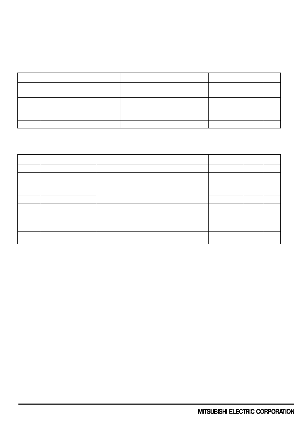
MAXIMUM RATINGS
(T
=+25°C, ZG=ZL=50, unless otherwise specified)
case
SYMBOL PARAMETER CONDITIONS RATING UNIT
V
V
P
P
T
case(OP)
T
Drain Voltage VGG<5V, Pin=0W 17 V
DD
Gate Voltage VDD<12.5V, Pin=50mW 6 V
GG
Input Power 100 mW
in
Output Power 45 W
out
Operation Case Temperature Range
Storage Temperature Range -40 to +110 °C
stg
f=450-520MHz,
VGG<5V
-30 to +100 °C
The above parameters are independently guaranteed.
ELECTRICAL CHARACTERISTICS
(T
=+25°C, ZG=ZL=50, unless otherwise specified)
case
SYMBOL PARAMETER CONDITIONS MIN TYP MAX UNIT
F Frequency Range 450 - 520 MHz
P
T
2f
I
GG
I
DD
— Stability
— Load VSWR Tolerance
Output Power VDD=12.5V 30 - - W
out
Total Efficiency VGG=5V 42 - - %
2ndHarmonic Pin=50mW - - -40 dBc
o
Input VSWR - - 3:1 —
in
Gate Current VDD=0V, VGG=5V, Pin=0W - 1 - mA
Leakage Current VDD=17V, VGG=0V, Pin=0W - - 1 mA
VDD=10.0-15.2V, Pin=25-70mW,
5<P
<40W (VGGcontrol), Load VSWR=3:1
out
VDD=15.2V, Pin=50mW,
P
=30W (VGGcontrol), Load VSWR=20:1
out
No parasitic oscillation —
No degradation or destroy —
All parameters, conditions, ratings, and limits are subject to change without notice.
Publication Date : Oct.2011
2
< Silicon RF Power Modules >
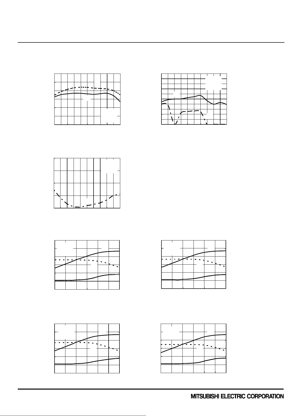
versus FREQUENCY
INPUT VSWR versus FREQUENCY
OUTPUT POWER, POWER GAIN and
OUTPUT POWER, POWER GAIN and
DRAIN CURRENT versus INPUT POWER
DRAIN CURRENT versus INPUT POWER
OUTPUT POWER, POWER GAIN and
OUTPUT POWER, POWER GAIN and
DRAIN CURRENT versus INPUT POWER
DRAIN CURRENT versus INPUT POWER
RA30H4552M1
RoHS Compliance, 450-520MHz 30W 12.5V, 2 Stage Amp. For MOBILE RADIO
TYPICAL PERFORMANCE (T
OUTPUT POWER, TOTAL EFFICIENCY, 2nd, 3rdHARMONICS versus FREQUENCY
70
60
(W)
out
50
40
30
20
TOTAL EFFICIENCY(%)
OUTPUT POWER P
10
430 440 450 460 470 480 490 500 510 520 530
5
(-)
4
in
r
3
2
INPUT VSWR
1
430 440 450 460 470 480 490 500 510 520 530
FREQUENCY f (MHz)
FREQUENCY f (MHz)
=+25°C, ZG=ZL=50, unless otherwise specified)
case
-30
h
T
P
out
-40
-50
-60
VDD=12.5V
VGG=5V
Pin=50mW
HARMONICS (dBc)
-70
-80
430 440 450 460 470 480 490 500 510 520 530
VDD=12.5V
VGG=5V
Pin=50mW
r
in
nd
2
FREQUENCY f (MHz)
VDD=12.5V
VGG=5V
Pin=50mW
rd
3
60
f=450MHz
VDD=12.5V
50
(dBm)
out
OUTPUT POWER P
VGG=5V
40
30
20
POWER GAIN Gp (dB)
10
I
DD
Gp
0
-10 -5 0 5 10 15 20
INPUT POWER Pin(dBm)
60
f=490MHz
VDD=12.5V
50
(dBm)
out
OUTPUT POWER P
VGG=5V
40
30
20
POWER GAIN Gp (dB)
10
I
DD
Gp
0
-10 -5 0 5 10 15 20
INPUT POWER Pin(dBm)
24
P
out
20
(A)
DD
16
12
8
4
DRAIN CURRENT I
0
60
f=470MHz
VDD=12.5V
50
(dBm)
out
VGG=5V
40
30
20
POWER GAIN Gp (dB)
10
OUTPUT POWER P
I
DD
Gp
P
out
0
24
20
16
12
8
4
0
(A)
DD
I
DRAIN CURRENT
-10 -5 0 5 10 15 20
INPUT POWER Pin(dBm)
24
P
out
20
(A)
DD
16
12
8
4
DRAIN CURRENT I
0
60
f=520MHz
50
40
VDD=12.5V
VGG=5V
(dBm)
out
30
20
POWER GAIN Gp (dB)
10
OUTPUT POWER P
I
DD
Gp
P
out
0
24
20
16
12
8
4
0
(A)
DD
DRAIN CURRENT I
-10 -5 0 5 10 15 20
INPUT POWER Pin(dBm)
Publication Date : Oct.2011
3
 Loading...