

Page 1

C
MIT
SUBIS
C
HI ELECTRI
MELSEC System Q
Programmable Logic Controllers
User's Manual
(Basic)
Serial Communication Modules
QJ71C24N/-R2/-R4, QJ71C24/-R2
Art. no.: 130031
01 09 2004
SH (NA)-080006
Version H
GX Configurator-SC
MITSUBISHI ELECTRI
INDUSTRIAL AUTOMATION
Page 2

Page 3
• SAFETY PRECAUTIONS •
(Always read these instructions before using this equipment.)
Before using this product, please read this manual and the relevant manuals introduced in this manual
carefully and pay full attention to safety to handle the product correctly.
The instructions given in this manual are concerned with this product. For the safety instructions of the
programmable controller system, please read the user's manual of the CPU module to use.
In this manual, the safety instructions are ranked as "DANGER" and "CAUTION".
DANGER
!
CAUTION
!
Note that the !CAUTION level may lead to a serious consequence according to t he circumstances.
Always follow the instructions of both levels because they are important to personal safety.
Please save this manual to make it accessible when required and always forw ard it to the end user.
Indicates that incorrect handling may cause hazardous conditions,
resulting in death or severe injury.
Indicates that incorrect handling may cause hazardous conditions,
resulting in medium or slight personal injury or physical damage.
[Design Instructions]
!
DANGER
•
See manuals of each data link for the operating status of each station when there is a
communication error in the data link.
There is the risk of an accident occurring due to output error or malfunctioning.
•
When using the notification function, the pager receiver may not be contacted due to the frequency
transmission status from the system setup environment and error on the receiver side.
To ensure the safety of the PLC system, install a call circuit with a lamp display or buzzer sound.
•
When performing the control of the PLC in operation (changing data) by connecting a peripheral
devices to the CPU module or personal computer, etc. to the intelligent device module, configure an
interlock circuit in a sequence program so the safety of the overall system is always maintained.
Also when performing other controls of the PLC in operation (changing program and operation
status (status control)), read this manual carefully and confirm if the overall safety is maintained.
Especially, when this control is performed to a remote PLC from an external dev ice, troubles
that have occurred on the PLC side may not be able to immediately be handled if there is a data
communication error.
Define a troubleshooting agreement between external devices and the PLC CPU for data
communication error occurrences, as well as construct an interlock circuit in the sequence program.
•
Do not write data into the "system area" of the buffer memory of intelligent function modules.
Also, do not use any "prohibited to use" signals as an output signal to an int elligent funct ion
module from the PLC CPU.
Writing data into the "system area" or outputting a signal for "prohibited to use" may cause a
PLC system malfunction.
A - 1 A - 1
Page 4
[Design Instructions]
!
CAUTION
•
Do not bunch the control wires or communication cables with the main circuit or power wires, or
install them close to each other.
They should be installed 100mm(3.9inch) or more from each other.
Not doing so could result in noise that may cause malfunction.
•
When using the module while values, such as buffer memory set values, are registered in the
Flash ROM, do not turn off the power supply for the module loading station nor reset the PLC
CPU.
If the power supply for the module loading station is turned off or the PLC CPU is reset while any
values are registered, the data contents in the Flash ROM become inconsistent and as a result the
values must be set again in the buffer memory, etc. and reregistered to the Flash ROM.
Also, this may cause failure and malfunction of the module.
[Installation Instructions]
!
CAUTION
•
Use the PLC in an environment that meets the general specifications contained in the user's
manual of the CPU module to use.
Using this PLC in an environment outside the range of the general specificat ions may cause
electric shock, fire, malfunction, and damage to or deterioration of the product.
•
While pressing the installation lever located at the bottom of module, insert the module fixing t ab
into the fixing hole in the base unit until it stops. Then, securely mount t he module with t he fixing
hole as a supporting point.
If the module is not installed properly, it may cause the module to malfunctio n, fail or fall o ff.
Secure the module with screws especially when it is used in an environment where constant
vibrations may occur.
•
Tighten the screws within the range of specified torque.
If the screws are loose, it may cause the module to fallout, short circuits, or malfunction.
If the screws are tightened too much, it may cause damage to the screw and/or the module,
resulting in fallout, short circuits or malfunction.
•
Switch all phases of the external power supply off when mounting or removing the module.
Not doing so may cause damage to the module.
•
Do not directly touch the conductive area or electronic components of the module.
Doing so may cause malfunction or failure in the module.
A - 2 A - 2
Page 5

[Wiring Instructions]
!
CAUTION
•
When turning on the power and operating the module after installation and wiring are completed,
always attach the terminal cover that comes with the product.
There is a risk of electric shock if the terminal cover is not attached.
•
Perform correct pressure-displacement, crimp-contact or soldering for external wire connections
using the tools specified by the manufactures.
Incorrect connection may cause short circuits, fire, or malfunction.
•
Attach connectors to the module securely.
•
Be sure to fix communication cables or power supply cables leading from the module by placing
them in the duct or clamping them.
Cables not placed in the duct or without clamping may hang or shift, allow ing them to be
accidentally pulled, which may cause a module malfunctio n and cable da mage.
•
Before connecting the cables, check the type o f interface to be connected.
Connecting or erroneous wiring to the wrong interface may cause failure to the module and
external devices.
•
Tighten the terminal screws within the range of specified torque.
If the terminal screws are loose, it may result in short circuits or malfunction.
If the screws are tightened too much, it may cause damage to the screw and/or the module,
resulting in fallout, short circuits or malfunction.
•
When removing the communication cable or power supply cable from the module, do not pull the
cable. When removing the cable with a connector, hold the connector on the side that is
connected to the module.
When removing the cable connected to the terminal block, first loosen the screws on the part
that is connected to the terminal block.
Pulling the cable that is still connected to t he module may cause malfunctio n or damage t o the
module or cable.
•
Be careful not to let foreign matters such as sawdust or wire chips get inside the module.
They may cause fires, failure or malfunction.
•
The top surface of the module is covered with protective film to prevent foreign objects such as
cable offcuts from entering the module when wiring.
Do not remove this film until the wiring is complete.
Before operating the system, be sure to remove the film to provide adequate heat ventilation.
A - 3 A - 3
Page 6
[Startup/Maintenance Instructions]
!
CAUTION
•
Do not disassemble or modify each module.
Doing so could cause failure, malfunction injury or fire.
•
Switch all phases of the external power supply off when mounting or removing the module.
Not doing so may cause failure or malfunction of the module.
•
not
Do
•
Do not touch the connector while the power is on.
•
Switch all phases of the external power supply off when cleaning or retightening ter minal screws
mount/remove the module onto/from base unit more than 50 times (IEC61131-2compliant), after the first use of the product.
Failure to do so may cause the module to malfunction due to poor contact of connector.
Doing so may cause malfunction.
and module installing screws.
Not doing so may cause failure or malfunction of the module.
If the screws are loose, it may cause the module to fallout, short circuits, or malfunction.
If the screws are tightened too much, it may cause damages to the screws and/or the module,
resulting in the module falling out, short circuits or malfunct ion.
•
Always make sure to touch the grounded metal to discharge the electricity charged in the body,
etc., before touching the module.
Failure to do so may cause a failure or malfunctions of the module.
[Operation Instructions]
!
CAUTION
•
When performing the control of the PLC in operation (especially changing data, program, and
operation status (status control)) by connecting a personal comput er, etc. to the intelligent
function module, read this manual carefully and confirm if the ov erall safety is maintained.
Failure to perform correct operation s to change data, program, or the status may result in
system malfunction, machine damage, or an accident .
[Disposal Instructions]
!
CAUTION
•
When disposing of this product, treat it as industrial waste.
A - 4 A - 4
Page 7
REVISIONS
The manual number is given on the bottom left of the back cover.
Print Date Manual Number Revision
Dec., 1999 SH (NA)-080006-A First Printing
Oct., 2000 SH (NA)-080006-B Add the contents of the function version B.
Correction
Contents, Entire manual (change MELSECNET/10H to MELSECNET/H),
About Manuals, About The Generic Terms and Abbreviations, Product
Configuration, Section 1.2, 1.2(8), 1.3 POINT, Section 2.2, 2.3, 2.5, 2.6,
Section 3.1, 3.6, 3.9, Section 4.2, 4.4.1(2)(a)(Figure), 4.6(1), Chapter
5(all), Section 6.1.1, 6.1.3, 6.1.4, Section 7.1.1, 7.1.2, 7.2.2, Section 8.1,
8.2.1, 8.2.2, 8.3.1, 8.3.2, Section 9.2 to 9.7, Section 10.1.1, 10.2.1,
10.3.8, 10.3.18, Appendix 1.1(2), Appendix 2(all), appendix 3(2),
Appendix 7, appendix 8
Addition
Entire manual (add the explanation on MELSECNET/H remote I/O
station), The Manual's Use and Structure, Section 2.1, Section
3.1(Table), Section 4.4.2( 1)( d), 4.9.2, Sec t ion 8.3.2 POINT, Section
10.2.1 (7164
H
, 7E70H), Appendix 3(1)
Jun., 2001 SH (NA)-080006-C Put Windows® base software product together from Mitsubishi
Programmable Logic Controller MELSEC Series to Mitsubishi integrated
FA Software MELSOFT Series.
Standardize the name from software package (GPP function) to Product
name (GX Developer).
Standardize the name from utility package (QSCU) to Product name (GX
Congifurator-SC).
Feb., 2002 SH (NA)-080006-D
Oct., 2002 SH (NA)-080006-E
Jan., 2003 SH (NA)-080006-F
Correction
Conformation to the EMC Directive and Low Voltage Instruction, About
the Generic Terms and Abbreviations, Product Configuration, Program
Examples (Section 6.1.4, 6.2.3, Section 7.2.3, Section 9.3, 9.5, Appendix-
8), Section 1.2(1)(d), 1.2(4)(b)(Diagram), 1.2(8)(b), 1.3, Section 2.1, 2.3,
2.4, 2.5, 2.7, Section 3.1(Table), 3.2.1(3) , 3.3. 3( 2), 3.4( T able) , 3.9,
Section 4.3, 4.5.2, Section 5.1.5(3), 5.2, Section 6.1.4, Section 8.2, 8.3.2
POINT, 8.4.2, 8.4.9(Table), 8.6.3(Table), 8.6.7(Table), Section 10.1.2(b),
10.3(Table), Appendix 1.1, 2.1, 6, 7, 9
Addition
Section 2.6, Section 8.4.4, 8.6.2(Table), Section 10.2.1(716F
10.2.3(7FE9
H
), 10.3.14, Appendix 3
H,
7FEFH),
Addition
About The Generic Terms and Abbreviations, Section 1.2, Section 2.1,
2.7, Section 4.5.2, Section 8.2.1, 8.2.2, Sec t ion 10.2.1, Appe ndix 1.1, 6
Addition
The Manual’s Use and Structure, About The Generic Terms and
Abbreviations, Sect ion 1.2(1) (4) , Sec t ion 2.1, 2.4, Sec tio n 5.2, Sec ti on
6.1.4, Section 9.8, Appendix 7
Addition model
QJ71C24N, QJ71C24N-R2, QJ71C24N-R4
A - 5 A - 5
Page 8
The manual number is given on the bottom left of the back cover.
Print Date Manual Number Revision
Jan., 2003 SH (NA)-080006-F
Addition
SAFETY PRECAUTIONS, About Manuals, About The Generic Terms
and Abbreviations, Product Configuration, Section 1.3, Section 2.1, 2.2,
2.3, 2.5, 2.6, 2.7, Section 3.1, 3.2.1, 3.3.1, 3.6, 3.8, 3.9, Section 4.1, 4.3,
4.4, 4.5, 4.6, 4.7.1, Section 6.1.1, 6.1.2, Section 7.1, 7.2.2, Chapter 8(all),
Section 9.1, 9.6, Section 10.1.2(b), 10.1.3(1), 10.2, Appendix 1, Appendix
2.1, Appendix 3, Appendix 5, Appendix 9
Jun., 2004 SH (NA)-080006-G
Correction
About The Generic Terms and Abbreviations, Product Configuration,
Chapter 2 (all), Section 3.8, Section 4.2.2 (1), Section 5.1.3 POINT,
Section 5.1.4, Chapter 8 (screen change), Section 8.6.10, Section 10.1.1,
Section 10.2
Addition
Appendix 9
Sep., 2004 SH (NA)-080006-H
Correction
Section 1.3, Section 2.5, 2.6, Section 3.5, 3.6, 3.9, Section 4.1, Chapter 8
(screen change), Section 8.6. 9, 8.6. 10, Sec t ion 10. 1, 10.2, Ap pen dix 1.1
Addition
Appendix 9.12
Japanese Manual Version SH-080001-L
This manual confers no industrial property rights or any rights of any other kind, nor does it confer any patent
licenses. Mitsubishi Electric Corporation cannot be held responsible for any problems involving industrial property
rights which may occur as a result of using the contents noted in this manual.
1999 MITSUBISHI ELECTRIC CORPORATION
A - 6 A - 6
Page 9

INTRODUCTION
Thank you for purchasing the MELSEC-Q series PLC.
Before using the equipment, please read this manual carefully to develop full familiarity with the functions
and performance of the Q series PLC you have purchased, so as to ensure correct use.
Please forward a copy of this manual to the end user.
CONTENTS (This manual)
SAFETY PRECAUTIONS..............................................................................................................................A- 1
REVISIONS....................................................................................................................................................A- 5
CONTENTS....................................................................................................................................................A- 7
About Manuals ...............................................................................................................................................A-15
Conformation to the EMC Directive and Low Voltage Instruction ................................................................A-15
The Manual’s Use and Structure ...................................................................................................................A-16
About The Generic Terms and Abbreviations...............................................................................................A-19
Definitions and Descriptions of Terminology.................................................................................................A-21
Product Configuration ....................................................................................................................................A-23
1 OVERVIEW 1- 1 to 1-11
1.1 Overview of the Serial Communication Module.....................................................................................1- 1
1.2 Features of the Serial Communication Module......................................................................................1- 2
1.3 About Added/Changed Functions in Function Version B......................................................................1-10
2 SYSTEM CONFIGURATION AND AVAILABLE FUNCTIONS 2- 1 to 2-14
2.1 Applicable Systems.................................................................................................................................2- 1
2.2 Combinations of PLC CPU and External Device, and Available Functions..........................................2- 3
2.3 For Use in Multiple CPU System............................................................................................................2- 6
2.4 For Use with Q00J/Q00/Q01CPU ..........................................................................................................2- 7
2.5 For Use at MELSECNET/H Remote I/O Station....................................................................................2- 8
2.6 Checking the Function Version, Serial No., and Software Version.......................................................2-12
3 SPECIFICATION S 3- 1 to 3-31
3.1 Performance Specifications....................................................................................................................3- 1
3.2 RS-232 Interface Specification...............................................................................................................3- 3
3.2.1 RS-232 connector specifications.....................................................................................................3- 3
3.2.2 RS-232 cable specification ..............................................................................................................3- 5
3.3 RS-422/485 Interface Specifications......................................................................................................3- 6
3.3.1 RS-422/485 terminal block specifications .......................................................................................3- 6
3.3.2 RS-422/485 cable specifications .....................................................................................................3- 7
3.3.3 Precautions when transferring data using RS-422/485 circuit .......................................................3- 8
3.4 Serial Communication Module Function List..........................................................................................3-11
3.5 Dedicated Instruction List........................................................................................................................3-12
3.6 Utility Package (GX Configurator-SC) Function List..............................................................................3-13
3.7 List of GX Devel op e r Se t tin g I tems for S e rial Co mmun i ca ti on M odule s...............................................3-14
3.8 List of Input/Output Signals for the PLC CPU........................................................................................3-15
3.9 List of Applications and Assignments of the Buffer Memory.................................................................3-17
A - 7 A - 7
Page 10

4 SETTINGS AND PROCEDURES PRIOR TO OPERATION 4- 1 to 33
4.1 Handling Precautions..............................................................................................................................4- 1
4.2 Settings and Procedures Prior to Operation .......................................................................................... 4- 2
4.3 Part Names and Functions .....................................................................................................................4- 3
4.4 External Wiring........................................................................................................................................ 4- 5
4.4.1 Connecting the RS-232 interface (full-duplex communications) ....................................................4- 6
4.4.2 Connecting the RS-422/485 interface .............................................................................................4- 8
4.5 Settings for GX Developer......................................................................................................................4-12
4.5.1 I/O assignment settings....................................................................................................................4-12
4.5.2 Switch settings for I/O and intelligent functional module ................................................................4-13
4.5.3 The Intelligent function module interrupt pointer setting.................................................................4-20
4.6 Settings with the Utility Package (GX Configurator-SC)........................................................................ 4-22
4.7 Individual Station Test.............................................................................................................................4-25
4.7.1 ROM/RAM/switch tests....................................................................................................................4-25
4.7.2 Individual station loopback test........................................................................................................4-28
4.8 Loopback Test......................................................................................................................................... 4-30
4.9 Maintenance and Inspection...................................................................................................................4-32
4.9.1 Maintenance and inspection............................................................................................................4-32
4.9.2 When mounting/dismounting the module........................................................................................4-33
5 DATA COMMUNICATION USING THE MELSEC COMMUNICATION PROTOCOL 5- 1 to 5- 6
5.1 Data Communication Functions .............................................................................................................5- 1
5.1.1 Accessing the PLC CPUs using the MC protocol...........................................................................5- 1
5.1.2 Message format and control procedure for data communication...................................................5- 2
5.1.3 PLC CPU setting for performing data communication....................................................................5- 2
5.1.4 Support of multiple CPU system or redundant system...................................................................5- 3
5.1.5 Support for the QCPU remote password function ..........................................................................5- 4
5.2 Utilizing the MX Component...................................................................................................................5- 6
6 DATA COMMUN I CA TI ON USI N G TH E N O N PR OC E DURE P R OTOC O L 6- 1 to 6-31
6.1 Data Reception from the External Device..............................................................................................6- 2
6.1.1 Receiving methods...........................................................................................................................6- 2
6.1.2 The receive area and the received data list ....................................................................................6- 6
6.1.3 Sequence program for data reception.............................................................................................6-11
6.1.4 Receive data clear............................................................................................................................6-14
6.1.5 How to detect reception errors.........................................................................................................6-17
6.1.6 Received data count and receive complete code settings .............................................................6-20
6.2 Sending Data to the External Device .....................................................................................................6-22
6.2.1 Transmission methods.....................................................................................................................6-22
6.2.2 Arrangement and contents of the transmission area and the transmission data...........................6-23
6.2.3 Sequence program for transmission data.......................................................................................6-25
6.2.4 How to detect transmission errors...................................................................................................6-28
6.3 Data Communications Precautions........................................................................................................6-30
A - 8 A - 8
Page 11

7 DATA COMMUNICATION USING THE BIDIRECTIONAL PROTOCOL 7- 1 to 7-28
7.1 Data Reception from the External Device..............................................................................................7- 2
7.1.1 Receiving methods...........................................................................................................................7- 2
7.1.2 Arrangement and contents of the receive area and the receive data............................................7- 4
7.1.3 Sequence program for data reception.............................................................................................7-10
7.1.4 How to detect reception errors.........................................................................................................7-13
7.1.5 Receive data clear............................................................................................................................7-14
7.2 Sending Data to the External Device .....................................................................................................7-15
7.2.1 Transmission methods.....................................................................................................................7-15
7.2.2 Arrangement and contents of the transmission area and the transmission data...........................7-16
7.2.3 Sequence program for data transmission.......................................................................................7-19
7.2.4 How to detect transmission errors...................................................................................................7-22
7.3 Processing when Simultaneous Transmission Performed During Full-Duplex Communications .......7-24
7.3.1 Processing when simultaneous transmissions occur .....................................................................7-24
7.3.2 Communication data processing when simultaneous transmissions occur...................................7-25
7.4 Data Communications Precautions........................................................................................................7-27
8 UTILITY PACKAGE (GX CONFIGURATOR-SC) 8- 1 to 8-51
8.1 Functions Available with Utility Package................................................................................................8- 2
8.2 Installing and Uninstalling Utility Package..............................................................................................8- 3
8.2.1 Usage precautions ...........................................................................................................................8- 3
8.2.2 Operating environment.....................................................................................................................8- 5
8.3 Explanation of Utility Package Operation...............................................................................................8- 6
8.3.1 Operation overview ..........................................................................................................................8- 6
8.3.2 Starting the intelligent function module utility
(displaying the [select parameter setting module] screen)........................................................................8-10
8.3.3 Performing common utility operations.............................................................................................8-13
8.4 System Registration to Flash ROM........................................................................................................8-16
8.4.1 User frame registration.....................................................................................................................8-18
8.4.2 Data for modem initialization registration ........................................................................................8-19
8.4.3 Data for modem connection registration .........................................................................................8-20
8.4.4 Modem function system setting/registration....................................................................................8-21
8.4.5 Transmission control and others system setting.............................................................................8-22
8.4.6 MC protocol system setting..............................................................................................................8-24
8.4.7 Non procedure system setting.........................................................................................................8-25
8.4.8 Bidirectional system setting .............................................................................................................8-26
8.4.9 PLC CPU monitoring system setting...............................................................................................8-27
8.4.10 Transmission user frame No. designation system setting............................................................8-29
8.4.11 Resetting the buffer memory/flash ROM setting values to the default values.............................8-30
8.4.12 Flash ROM write allow/prohibit setting..........................................................................................8-30
8.5 Auto Refresh Setting...............................................................................................................................8-31
8.6 Monitor/Test ............................................................................................................................................8-32
8.6.1 X · Y monitor/test..............................................................................................................................8-33
8.6.2 Modem function monitor/test ...........................................................................................................8-34
8.6.3 Transmission control and others monitor/test.................................................................................8-37
8.6.4 MC protocol monitor......................................................................................................................... 8-39
A - 9 A - 9
Page 12

8.6.5 Non procedure monitor/test .............................................................................................................8-41
8.6.6 Bidirectional monitor.........................................................................................................................8-43
8.6.7 PLC CPU monitoring monitor ..........................................................................................................8-44
8.6.8 Transmission user frame No. designation monitor .........................................................................8-46
8.6.9 Monitor/test others............................................................................................................................8-47
8.6.10 Display LED off and communication error information/error code initialization...........................8-49
8.7 Non Procedure Protocol Receive Data Clear ........................................................................................8-51
9 DEDICATED INSTRUCTIONS 9- 1 to 9-21
9.1 Dedicated Instruction List........................................................................................................................9- 1
9.2 ONDEMAND Instruction .........................................................................................................................9- 2
9.3 OUTPUT Instruction................................................................................................................................9- 5
9.4 INPUT Instruction....................................................................................................................................9- 8
9.5 BIDOUT Instruction.................................................................................................................................9-11
9.6 BIDIN Instruction.....................................................................................................................................9-14
9.7 SPBUSY Instruction................................................................................................................................9-17
9.8 CSET (Receive data clear).....................................................................................................................9-19
10 TROUBLESHOOTING 10- 1 to 10-43
10.1 Checking the Status of the Serial Communication Module...............................................................10- 1
10.1.1 Checking the LED ON status, communications error status, and switch setting status of
the serial communication module................................................................................................10- 1
10.1.2 Initializing error information of the serial communication module...............................................10- 6
10.1.3 Reading the RS-232 control signal status...................................................................................10- 9
10.1.4 Reading the data communication status (Transmission sequence status) ...............................10-10
10.1.5 Reading the switch setting status................................................................................................10-11
10.1.6 How to read the current operation status....................................................................................10-13
10.2 Error Code Tables...............................................................................................................................10-15
10.2.1 Error code table............................................................................................................................10-15
10.2.2 A compatible 1C frame communications error code table..........................................................10-24
10.2.3 Error code list while modem function is used..............................................................................10-25
10.3 Troubleshooting by Symptom.............................................................................................................10-27
10.3.1 Troubleshooting when "RUN" LED is turned OFF......................................................................10-29
10.3.2 Troubl e sho ot in g wh en "R D" LE D doe s not bli n k even th ou gh an e xte r nal dev i ce is
transmitting a message................................................................................................................10-30
10.3.3 Troubleshooting when the Q series C24 does not return a response message even
though an external device transmitted a message and the "RD" LED blinked..........................10-31
10.3.4 Troubleshooting when an external device transmitted a message and "RD" LED blinked,
but the Read Request signal was not turned ON .......................................................................10-32
10.3.5 Troubleshooting when communication error "NAK" generates..................................................10-33
10.3.6 Troubleshooting when communication error "C/N" generates ...................................................10-33
10.3.7 Troubleshooting when communication error "P/S" generates....................................................10-34
10.3.8 Troubleshooting when communication error "PRO." generates.................................................10-35
10.3.9 Troubleshooting when communication error "SIO" generates ...................................................10-36
10.3.10 Troubleshooting when communication error "CH1 ERR.", "CH2 ERR." generate..................10-37
10.3.11 Troubleshooting when communications is intermittently established and lost ........................10-38
10.3.12 Troubleshooting when data that cannot be decoded is transmitted and received ..................10-39
A - 10 A - 10
Page 13

10.3.13 Troubleshooting when it is unclear whether the communication error cause is in
the Q series C24 or an external device ....................................................................................10-40
10.3.14 Troubleshooting when data cannot be communicated via modem..........................................10-41
10.3.15 Troubleshooting when data cannot be communicated with the ISDN sub-address................10-42
10.3.16 Troubleshooting when constant cycle transmission does not operate normally......................10-42
10.3.17 Troubleshooting when condition agreement transmission does not operate normally ...........10-42
10.3.18 Troubleshooting when data cannot be received by an interrupt program ...............................10-42
10.3.19 Troubleshooting when data cannot be written to Flash ROM..................................................10-42
10.3.20 Troubleshooting when the "ERR" LED is lit ..............................................................................10-43
APPENDIX APP.- 1 to APP.-58
Appendix 1 Functional Improvements of the Q Series C24 ...................................................................App.- 1
Appendix 1.1 Comparison of the Functions of Q Series C24/GX Configurator-SC...........................App.- 1
Appendix 1.2 Pr e caut io n s w hen U pda ti ng th e Mo du le fro m Fu n ction Version A to B.......................App.- 5
Appendix 2 QnA/A Series Module...........................................................................................................App.- 6
Appendix 2.1 Functional Comparison with the Q series C24 and the QnA/A Series Modules .........App.- 6
Appendix 2.2 Using Programs Designed for the QC24 (N) and Installing the Q Series C24
into Existing Systems ....................................................................................................App.- 8
Appendix 2.2.1 Using programs designed for the QC24 (N).....................................................App.- 8
Appendix 2.2.2 Installing on existing systems...........................................................................App.- 9
Appendix 2.3 Using Programs Designed for the Computer Link Module and Installing
the Q Series C24 into Existing Systems......................................................................APP.-10
Appendix 2.3.1 Using programs designed for the computer link module..................................App.-10
Appendix 2.3.2 Installing the Q series C24 into existing systems.............................................App.-13
Appendix 3 Processing Time...................................................................................................................App.-14
Appendix 4 ASCII-Code Table.................................................................................................................App.-17
Appendix 5 External Dimensions.............................................................................................................App.-18
Appendix 6 Example of Connection when a Converter is Used.............................................................App.-20
Appendix 7 Communication Support Tool (MX Component) .................................................................App.-23
Appendix 7.1 Overview of MX Component .........................................................................................App.-23
Appendix 7.2 Usage Procedure of MX Component............................................................................App.-26
Appendix 8 Example of Clear Process Program for Receive Data........................................................App.-30
Appendix 9 Program Examples for Using Q Series C24 at MELSECNET/H Remote I/O Station........App.-32
Appendix 9.1 System configuration and program conditions .............................................................App.-32
Appendix 9.2 When accessing buffer memory using sequence program..........................................App.-34
Appendix 9.3 When sending on-demand data....................................................................................App.-35
Appendix 9.4 When receiving data using nonprocedural or bidirectional protocol ............................App.-37
Appendix 9.5 When sending data using nonprocedural or bidirectional protocol..............................App.-39
Appendix 9.6 When clearing received data.........................................................................................App.-41
Appendix 9.7 When sending data using user frames .........................................................................App.-43
Appendix 9.8 When performing initial setting......................................................................................App.-46
Appendix 9.9 When registering user frame.........................................................................................App.-48
Appendix 9.10 When reading user frame............................................................................................App.-50
Appendix 9.11 When deleting user frame...........................................................................................App.-52
Appendix 9.12 When changing the communication protocol and transmission setting.....................App.-54
Appendix 10 Setting Value Recording Sheet..........................................................................................App.-57
INDEX Index- 1 to Index- 2
A - 11 A - 11
Page 14

(Related Manual-1) … Q Corresponding Serial Communication Module User's Manual (Application)
SH-080007-G
1 OVERVIEW
1.1 Overview
1.2 Functions Added/Changed by Function
Version B
2 USING THE PLC CPU MONITORING
FUNCTION
2.1 Overview
2.2 About the PLC CPU Monitoring Function
2.3 Settings for Using the PLC CPU Monitoring
Function
2.4 Precautionary Notes for Using the PLC CPU
Monitoring Function
3 COMMUNICATIONS BY THE MODEM
FUNCTION
3.1 Overview
3.2 System Configuration
3.3 Specifications
3.4 Start-up of the Modem Function
3.5 Sample Programs
4 RECEIVING DATA WITH AN INTERRUPT
PROGRAM
4.1 Settings for Receiving Data Using an Interrupt
Program
4.2 Interrupt Program Startup Timing
4.3 Reception Control Method Using an Interrupt
Program
4.4 Programming
5 CHANGING SEND AND RECEIVE DATA
LENGTH UNITS TO BYTE UNITS
(WORD/BYTES UNITS SETTING)
6 CHANGING THE DATA COMMUNICATIONS
MONITORING TIMES
6.1 No-Reception Monitoring Time (timer 0)
Setting
6.2 Response Monitoring Time (timer 1) Setting
6.3 Transmission Monitoring Time (timer 2)
Setting
6.4 Message Wait Time Setting
7 DATA COMMUNICATIONS USING DC CODE
TRANSMISSION CONTROL
7.1 Control Contents of DTR/DSR (ER/DR)
Signal Control
7.2 Control Contents of DC Code Control
7.3 Precautions when Using the Transmission
Control Functions
8 DATA COMMUNICATIONS USING HALF-
DUPLEX COMMUNICATIONS
8.1 Half-duplex Communications
8.2 Data Transmission and Reception Timing
8.3 Changing the Communication System
8.4 Connector Connections for Half-duplex
Communications
8.5 Half-duplex Communications Precautions
9 CONTENTS AND REGISTRATION OF THE
USER FRAMES FOR DATA COMMUNICATION
9.1 User Frame Types and Contents During
Communication
9.2 Transmission/Reception Processing Using
User Frame Register Data
9.3 Precautions when Registering, Reading,
Deleting and Using User Frames
9.4 Register/Read/Delete User Frames
10 ON-DEMAND DATA COMMUNICATIONS
USING USER FRAMES
10.1 User Frame Data Communications Function
10.2 User Frame Types and Registration
10.3 User Frame On-Demand Data Transmission
and Buffer Memory Used
10.4 On-Demand Function Control Proc ed ur e
During User Frame Use
10.5 Example of an On-Demand Data
Transmission Program Using User Frames
11 DATA COMMUNICATIONS USING USER
FRAMES
11.1 Overview of Data Communication
Procedure
11.2 Data Reception
11.3 Receive Program
11.4 Data Transmission
11.5 Transmission program
12 TRANSPARENT CODES AND ADDITIONAL
CODES
12.1 Handling the Transparent Code and
Additional Code Data
12.2 Registering Transparent Codes and
Additional Codes
12.3 Handling Transparent Codes and Additional
Codes During Non Procedure Protocol Data
Communication
12.4 Example of Data Communication Using the
Non Procedure Protocol
12.5 Handling Transparent Codes and Additional
Codes During Bidirectional Protocol Data
Communication
12.6 Example of Data Communication Using the
Bidirectional Protoc o l
A - 12 A - 12
Page 15

(Related Manual-1) … Q Corresponding Serial Communication Module User's Manual (Application)
SH-080007-G
13 COMMUNICATING WITH ASCII CODE (ASCII-
BIN CONVERSION)
13.1 ASCII-BIN Conversion
13.2 Settings for ASCII-BIN Conversion
13.3 Performing ASCII-BIN Conversion for Data
Communicated via Non Procedure Protocol
13.4 Example of Data Communication Using the
Non Procedure Protocol
13.5 Performing ASCII-BIN Conversion for Data
Communicated Via the Bidirectional Protocol
13.6 Example of Data Communication Using the
Bidirectional Protoc o l
14 DATA COMMUNICATIONS USING EXTERNAL
DEVICE AND PLC CPU M : N
CONFIGURATION
14.1 Data Communications Precautions
14.2 External Devices Interlock Conditions
14.3 Examples of Procedure for Data
Communications with the PLC CPU
15 SWITCHING THE MODE AFTER STARTING
15.1 Mode Switching Operation and Contents
that can be Changed
15.2 Mode Switching Precautions
15.3 I/O Signals for Handshake with PLC CPU
and Buffer Memory
15.4 Switching the Mode from the PLC CPU
15.5 Switching the Mode from an External Device
16 USING COMMUNICATION DATA
MONITORING FUNCTION
16.1 Communication Data Monitoring Function
16.2 Communication Data Monitoring Function
Settings
16.3 Communication Data Monitoring Example
17 DEDICATED INSTRUCTIONS
17.1 Dedicated Instruction List
17.2 BUFRCVS Instruction
17.3 CSET Instruction (PLC CPU Monitoring
Register/Cancel)
17.4 CSET Instruction (Initial Settings)
17.5 GETE Instruction
17.6 PRR Instruction
17.7 PUTE Instruction
17.8 UINI Instruction
A - 13 A - 13
Page 16

(Related Manual-2) … Q Corresponding MELSEC Communication Protocol Reference Manual
SH-080008-F
1 OVERVIEW
1.1 Overview of the MELSEC Communication
Protocol
1.2 Features of the MELSEC Communication
Protocol
2 DATA COMMUNICATION USING THE MELSEC
COMMUNICATION PROTOCOL
2.1 Types and Applications of Data
Communication Frames
2.2 Accessible Range of Each Data
Communication Frames
2.3 How to Read the Control Procedures of the
MC Protocol
2.4 Access Timing of the PLC CPU Side
2.5 Setting Method for Writing to the PLC CPU
during RUN
2.6 Accessing Other Stations
2.7 Precautions on Data Communication
2.8 Time Chart and Communication Time of the
Transmission Sequence of the Serial
Communication Module
2.9 Transmission Time When Accessing Other
Stations Via MELSEC NE T/H, MELSE CNE T/ 10
2.10 Compatibilit y with Multip le CPU Systems
2.11 Compatibility with the Q00CPU, Q01CPU
Serial Communication Function
3 WHEN COMMUNICATING USING THE QnA
COMPATIBLE 3E/3C/4C FRA M ES
3.1 Message Formats
3.2 List of Commands and Functions for the QnA
Compatible 3E/3C/4C Frames
3.3 Device Memory Read/Write
3.4 Buffer Memory Read/Write
3.5 Reading from and Writing to the Buffer
Memory of an Intelligent Function Module
3.6 PLC CPU Status Control
3.7 Drive Memory Defragmentation (for Other
Station QnACPU)
3.8 File Control
3.9 Registering, Deleting and Reading User
Frames: for Serial Communication Modules
3.10 Global Function: for Serial Communication
Modules
3.11 Data Transmission to an External device
(On-Demand Function): for Serial
Communication Modules
3.12 Initializing the Transmission Sequence: for
Serial Communication Modules
3.13 Mode Switching: for Serial Communication
Module
3.14 Turning Off Displayed LEDs and Initializing
Communication Error Information and Error
Code: for Serial Communication Module
3.15 Turning Off the COM.ERR LED: for Ethernet
Modules
3.16 Loopback Test
3.17 Registering or Canceling PLC CPU
Monitoring: for Serial Communication
Modules
3.18 Remote Password Unlock/Lock
4 WHEN COMMUNICATING USING THE QnA
COMPATIBLE 2C FRAMES
4.1 Control Procedures and Message Formats
4.2 Contents of the Data Designation Items
4.3 List of Commands and Functions for QnA
Compatible 2C Frames
4.4 Precautions on the Data Communication
4.5 Example of Data Communication Using QnA
Compatible 2C Frames
5 WHEN COMMUNICATING USING THE A
COMPATIBLE 1C FRAMES
5.1 Control Procedures and Message Formats
5.2 Device Memory Read/Write
5.3 Extension File Register Read and Write
5.4 Reading and Writing in the Buffer Memory of
an Intelligent Function Module
5.5 Loopback Test
6 WHEN COMMUNICATING USING THE A
COMPATIBLE 1E FRAMES
6.1 Message Formats and Control Procedures
6.2 List of Commands and Functions for A
Compatible 1E Frames
6.3 Device Memory Read/Write
6.4 Extension File Register Read and Write
6.5 Reading and Writing in the Buffer Memory of
an Intelligent Function Module
APPENDIX
Appendix-1 Reading and Writing by Designation
of the Device Memory Extension
Appendix 2 Reading from and Writing to the
Buffer Memory
Appendix-3 Processing Time of the PLC CPU
Side While Communicating Using
the MC Protocol
A - 14 A - 14
Page 17

About Manuals
The following table lists the manuals relating to this product. Please order the desired manual(s) as needed.
Related manuals
Manual Name
Q Corresponding Serial Communication Module User's Manual (Application)
This manual explains the specifications and operating procedures for the special module functions, the
settings for use of special functions, and data-communication method for use with external devices.
(sold separately)
Q Corresponding MELSEC Communication Protocol Reference M anual
This manual explains how the external devices read and write PLC CPU data through communication
with the MC protocol using the serial communication module/Ethernet module.
(sold separately)
GX Configurator-SC Version 2 Operating Manual (Protocol FB support function)
This manual explains the function and usage of the protocol FB support function that supports the
creation of the data communication program of the module and set up of each parameter.
(sold separately)
Conformation to the EMC Directive and Low Voltage Instruction
For details on making Mitsubishi PLC conform to the EMC directive and low voltage
instruction when installin g it in your pro duct, ple as e see Cha pter 3, "EM C Dir ec tive
and Low Voltage Instruction" of the User's Manual (Hardware) of the CPU module to
use.
The CE logo is printed on the rating plate on the main body of the PLC that conforms
to the EMC directive and low voltage instruction.
Manual Number
(Model Code)
SH-080007
(13JL87)
SH-080008
(13JF89)
SH-080393E
(13JU46)
By making this product conform to the EMC directive and low voltage instruction, it is
not necessary to make those steps individually.
A - 15 A - 15
Page 18

The Manual's Use and Structure
How to use this manual
In this manual, details of the serial communication modules (QJ71C24N,
QJ71C24N-R2, QJ71C24N-R4, QJ71C24 and QJ71C24-R2) are organized as
shown below, according to their applications.
Please use this manual using the contents below as a reference.
(1) To learn about features, functions and comp onent par ts
(a) To learn about features and functions
(b) To learn about the packed items and system-configured items
(2) To learn about processing requir ed to start up the ser i al
communication module
• Chapter 1 describes the features of the serial communication modules.
• Chapter 3 describes the common specifications and functions of the serial
communication modules.
• The section prior to Chapter 1, "Product Configuration", describes the
parts that are packed along with the serial communication module.
• Parts and components other than those packed with the module must be
prepared separately by the user.
(a) To learn about the startup procedure
• Section 4.2 describes the general procedures prior to starting the
operation of the serial communication module.
(b) To learn about the connection with the external devices
• Section 4.4 describes the connection methods for each type of interface.
(c) To learn about processing required prior to operation of the serial
communication module
• Section 4.5 explains the parameter settings with GX Developer in order to
use the serial communication module.
• Section 4.6 and Chapter 8 describe the settings from GX Configurator-SC
to perform the initial setting of the serial communication module.
To change an initial value, follow the procedure described in Chapter 8.
(d) To check for failure in the serial communication module
• Section 4.7 describes the test of the individual serial communication
module.
(e) To learn how to check for a connection error with the external devices
• Section 4.8 describes how to perform the individual module test and the
loopback test using MC protocol-based communication.
Details of the loopback test command are described in the reference
manual.
A - 16 A - 16
Page 19

(3) To learn about data communication functi ons and d etai l ed
explanations
(a) To learn about the communication functions
• Section 3.4 describes an overview of the serial communication module
functions.
(b) To learn about detailed explanations of the communication functions
• The basic communication methods are described in Chapters 5 to 7.
• Special functions are described in the User's Manual (Application).
(4) To learn about data communication functi ons and programming
(a) To learn how to read data from and written to the PLC CPU
• Data is read from and written to the PLC CPU with a communication
function using the MC protocol.
Details are described in the Reference Manual.
• Appendix 7 describes an overview of the communication support tool (MX
Component) that supports communication using the MC protocol.
(b) To learn how to send and receive data between the PLC CPU and the
external devices
• Data communica ti on be twee n t he PLC CPU an d th e exte r na l de vi ce s is
performed with a communication function using the non procedure
protocol or the bidirectional protocol.
• Chapter 6 explains details of the communication functions and
programming using the non procedure protocol.
• Chapter 7 explains details of the communication functions and
programming using the bidirectional protocol.
(5) To learn how to check for error occurrences and take corr ective
actions
Chapter 10 de scribe s t roub l esho o tin g, how t o che ck for e rr or s, an d de taile d
explanations of error codes.
(6) To learn about functions that have been adde d or chang ed i n
function version B
• Section 1.3 li sts th e fun c ti on s th at have been added or change d a s well as
manuals that provide detailed explanations hereof.
• Appendix 1.1 provides a breakdown of the functions of Q series C24/GX
Configurator-SC by function version/software version.
A - 17 A - 17
Page 20

The structure of this manual
The module's buffer memory stores default values that are used as initial settings
to execute the data send/receive functions in order to communicate with the
external devices.
Data can be sent to or received from the external devices using these default
values. However, it may be necessary to change the default values, depending on
system specifications.
This manual explains how to perform the initial settings in order to use each
function of the utility package available for this module (GX-Configurator-SC).
When changing a default value for sending and receiving data to/from an opposite
device, first see the section describing the applicable function to verify the initial
setting item and setting value you wish to change, then change the default value
as explained in Chapter 8.
A - 18 A - 18
Page 21
About The Generic Terms and Abbreviations
This manual uses the following generic terms and abbreviations to describe the serial communication
modules, unless otherwise specified.
(1) Generic terms and abbreviati ons of relevant modules
In this manual, the following generic terms and abbreviations are used to indicate
the PLC CPU and other modules used for the data-communication functions of
the serial communication modules. Module model names are provided when
relevant model names are needed to be shown.
Generic term/abbreviation Description of generic term/abbreviation
Abbreviation for QJ71C24N, QJ71C24N-R2, QJ71C24N-R4, QJ71C24 and QJ71C24-R2 type serial
Q series C24 (C24)
QC24 Generic term for AJ71QC24, AJ71QC24-R2, AJ71QC24-R4, A1SJ71QC24, A1SJ71QC24-R2.
QC24N
QC24(N) Generic term for QC24, QC24N.
QCPU Q mode
QCPU station Abbreviation for the PLC with QCPU installed.
QnACPU
Q/QnACPU Generic term for QCPU, QnACPU.
UC24
Computer link module
Serial communication module
communication modules.
(Indicated as "C24" in the diagrams)
Generic term for AJ71QC24N, AJ71QC24N-R2, AJ71QC24N-R4, A1SJ71QC24N, A1SJ71QC24NR2.
Generic term for Q00JCPU, Q00CPU, Q01CPU, Q02CPU, Q02HCPU, Q06HCPU,
Q12HCPU, Q25HCPU, Q12PHCPU, Q25PHCPU.
Generic term for Q2ACPU, Q2ACPU-S1, Q2ASCPU, Q2ASCPU-S1, Q2ASHCPU, Q2ASHCPU-S1,
Q3ACPU, Q4ACPU, Q4 AR C P U .
Generic term for AJ71UC24, A1SJ71UC24-R2, A1SJ71UC24-R4, A1SJ71UC24-PRF,
A1SJ71C24-R2, A1SJ71C24-R4, A1SJ71C24-PRF, A2CCPUC24, A2CCPUC24-PRF.
A series computer link modules.
Generic term for the module below.
AJ71QC24, AJ71QC24-R2, AJ71QC24-R4, A1SJ71QC24, A1SJ71QC24-R2,
QnA series
Q series QJ71C24N, QJ71C24N-R2, QJ71C24N-R4, QJ71C24, QJ71C24-R2
AJ71QC24N, AJ71QC24N-R2, AJ71QC24N-R4, A1SJ71QC24N, A1SJ71QC24NR2.
A - 19 A - 19
Page 22

(2) Other generic terms and abbrevi ati ons
This manual uses the following generic terms and abbreviations to explain the
data-communication devices for the serial communication module. The
names/model names are provided when it is necessary to explicitly identify the
model being discussed.
Generic term/abbreviation Description of generic term/abbreviation
Buffer memory
Computer
Data communication functions Generic term for MC protocol, non procedure protocol, and bidirectional protocol.
GX Configurator-SC
GX Developer Abbreviation for GX Developer (SWnD5C-GPPW-E). (n in the model should be 4 or greater)
I/F Abbreviation for inte r fa ce
Intelligent function module devices
Intelligent function modules
MELSECNET/10 Abbreviation for MELSECNET/10 network system.
MELSECNET/H Abbreviation for MELSECNET/H network system.
MX Component Abbreviation for MX Component (SW0D5C-ACT-E or later).
Operating Manual
(Protocol FB support function)
Opposite devices
(external devices)
Reference Manual Q Corresponding MELSEC Communication Protocol Reference Manual
RS-232 (interface) Abbreviation for interface conforming to RS-232.
RS-422/485 (interface) Abbreviation for interface conforming to RS-422 and RS-485.
Special function modules
Switch setting Generic term for intelligent function module switch setting
User's Manual (Application) or
Application
User's Manual (Basic) or Basic Q Corresponding Serial Communication Module User's Manual (Basic)
Generic term for memory of the intelligent function modules/special function modules used for
storing data sent to or received from the PLC CPU (setting values, monitor values, etc.)
Generic term for one of the external devices with which data can be sent/received using the MC
protocol or the bidirectional protocol.
Abbreviation for GX Configurator-SC (SW0D5C-QSCU-E or later).
• Initial settings for the module, monitoring and testing can be performed without using a sequence
program and without considering I/O signals or buffer memory. (Intelligent function utility)
• Converting sequence programs necessary for data communication processing into FB can
shorten program production man-hours.
In addition, the monitoring and analysis of the transmitted/received data by the communication
network can shorten the system start-up time. (Protocol FB support function)
Generic term for buffer memory of the intelligent function modules used for storing data sent to or
received from the PLC CPU (setting values, monitor values, etc.)
Generic term for the Q series PLC modules that are operated by commands from the PLC CPU
(equivalent to the A series PLC special function modules).
Examples:
• CC-Link interface module
• A/D and D/A conversion modules
• Ethernet interface module
• Serial communication module
GX Configurator-SC Version 2 Operating Manual (Protocol FB support function)
Generic term for computers, indicators, measuring instruments, ID modules, bar code readers,
regulators, other serial communication modules, UC24, etc. that are connected to this serial
communication module for data communication.
Generic term for the A/QnA series PLC modules that are operated by commands from the PLC
CPU (equivalent to the Q series PLC intelligent function modules).
Examples:
• CC-Link interface module
• A/D and D/A conversion modules
• High-speed counter module
• Ethernet interface module
• Computer link module and serial communication module
Q Corresponding Serial Communication Module User's Manual (Application)
A - 20 A - 20
Page 23

Definitions and Descriptions of Terminology
The following table lists the definitions and descriptions of terminology used in this manual and related
manuals for the Q series serial communication modules.
Terms Description
One of the message formats for the serial communication module for performing communication
using the MC protocol and ASCII code data.
A compatible IC fra me
(Formats 1 to 4)
Bidirectional protocol
Independent operation
Linked operation
MELSEC communication protocol
(MC protocol)
Message send function
(Printer function)
Multidrop connection
Non procedure protocol
QnA compatible 2C frame
(Formats 1 to 4)
QnA compatible 3C frame
(Formats 1 to 4)
QnA compatible 4C frame
(Formats 1 to 4)
This is the same message format as when communicating using the protocol for the A series
computer link modules. Device memory read/write operations for the QCPU are allowed within
the device range of the AnACPU.
For details, see Chapter 5 of the Reference Manual.
A communication procedure for the serial communication modules and one of the data
communication functions for communicating any data between the PLC CPU and an opposite
device. Details are explained in Chapter 7.
A mode of interface operation to communicate data with external devices using a function
specified in each communication protocol setting. Two interfaces of serial communication
modules do not interact.
The operation mode of each of the two interfaces for a serial communication module that are
connected to external devices and linked to one another in order to send/receive data to/from the
external devices.
The two interfaces communicate data using the identical data-communication function (MC
protocol (identical format) or non procedure protocol) and the identical transmission
specifications. (Linked operation using the bidirectional protocol is not allowed.)
A communication procedure for the Q series serial communication modules or the Ethernet
interface modules, and a name of communication method for accessing to the PLC CPU from an
opposite device. (This is called the MC protocol in this manual.)
There are two communication methods; one uses ASCII code data and the other uses binary
code data.
Details are explained in the Reference Manual.
This function registers character data (messages) to be sent to external devices (mainly printers)
in the serial communication module as an user frame in advance, and sends the registered data
for multiple user frames using the non procedure protocol (sent by an instruction from the PLC
CPU).
A name of the connection when multiple external devices or other serial communication modules are
connected in a 1:n or m:n mode using the serial communication module's RS-422/485 interface.
An user's communication procedure and one of the data communication functions for
communicating any data between the PLC CPU and an opposite device. Details are explained in
Chapter 6.
One of the message formats for the serial communication module for performing communication
using the MC protocol and ASCII code data.
This is the same message format as the communication frame using the protocol for the QnA
series serial communication modules.
• QnA compatible 2C frame (Formats 1 to 4): QnA simplified frame (Formats 1 to 4)
Details are explained in Chapter 4 of the Reference Manual.
One of the message formats for the serial communication module for performing communication
using the MC protocol and ASCII code data.
This is the same message format as the communication frame using the protocol for the QnA
series serial communication modules.
• QnA compatible 3C frame (Formats 1 to 4): QnA frame (Formats 1 to 4)
• QnA compatible 4C frame (Formats 1 to 4): QnA extension frame (Formats 1 to 4)
Details are explained in Chapter 3 of the Reference Manual.
A - 21 A - 21
Page 24

Terms Description
QnA compatible 4C frame
User frame
(Format 5)
One of the message formats for the serial communication module for performing communication
using the MC protocol and binary code data.
This is the same message format as the communication frame using the protocol for the QnA
series serial communication modules.
• QnA compatible 4C frame (Format 5): QnA extension frame (Format 5)
Details are explained in Chapter 3 of the Reference Manual.
Data name when the fixed format portion of messages to be sent or received between a serial
communication module and an opposite device is registered in the module and used for sending
and receiving data with the functions listed below. (The contents of an user frame data should
conform to the specifications of the opposite device).
The data array of the head and tail sections of a message (transmission control code, C24 station
number, sum check, fixed data, etc.) to be sent and received is registered in the serial
communication module before use.
• MC protocol on-demand function.
• Data communication function using the non procedure protocol.
Details are explained in Chapter 9 of the User's Manual (Applications).
A - 22 A - 22
Page 25
Product Configuration
The following lists the product configuration of the Q series serial communication modules.
Model Item name Quantity
QJ71C24N serial communication module or QJ71C24 seria l
QJ71C24N or QJ71C24
QJ71C24N-R2 or
QJ71C24-R2
QJ71C24N-R4
SW2D5C-QSCU-E GX Configurator-SC Version 2 (1-license product) (CD-ROM) 1
SW2D5C-QSCU-EA GX Configurator-SC Version 2 (Multiple-license product) (CD-ROM ) 1
communication module
Terminal resistor 330 1/4 W (for RS-422 communication)
Terminal resistor 110 1/2 W (for RS-485 communication)
QJ71C24N-R2 serial communication module or QJ71C24-R 2 serial
communication module
QJ71C24N-R4 serial communication module 1
RS-422/485 plug-in connector socket block 2
Terminal resistor 330 1/4 W (for RS-422 communication)
Terminal resistor 110 1/2 W (for RS-485 communication)
Plate terminal (for connecting a braided shield cable) 4
1
2
2
1
4
4
A - 23 A - 23
Page 26
1 OVERVIEW
1 OVERVIEW
MELSEC-Q
1
This manual describes the specifications for the QJ71C24N, QJ71C24N-R2,
QJ71C24N-R4, QJ71C24, QJ71C24-R2 serial communication module (hereinafter
referred to as "Q series C24"), as well as the procedures prior to starting the operation,
maintenance, inspection, data communication methods for use with external devices
and troubleshooting.
When applying the following program examples to the actual system, make sure to
examine the applicability and confirm that it will not cause system control problems.
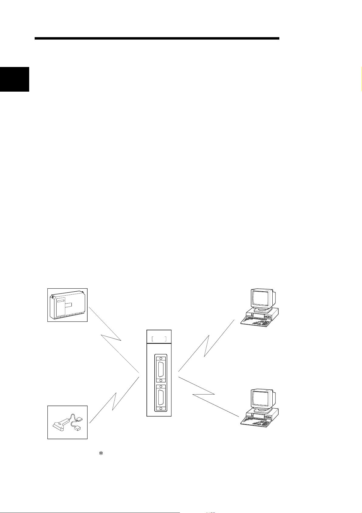
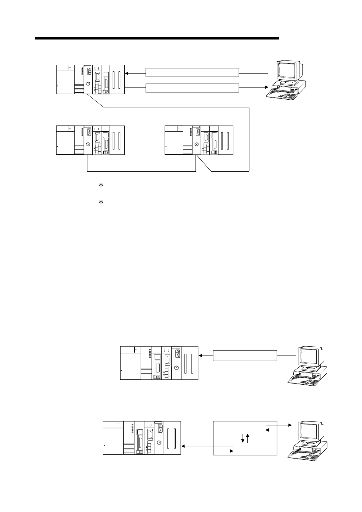
1.1 Overview of the Serial Communi cati on M odule
The Q series C24 is a module that connects the Q series PLC CPU and an external
device using an RS-232 or RS-422/485 line for serial communication, in order to
achieve the data communication described below.
By using a modem/terminal adapter, a public line (analog/digital) can be used for data
communication with a remote location.
• PLC data collection/change from the external devices
(See the MELSEC Communication Protocol Reference Manual.)
• PLC monitoring and control from the external devices (See Chapter 2 of the User's
Manual (Application).)
• Data receiving and sending in any formats that conform to the external device
specifications (See (2) and (3) of Section 1.2.)
• Collection of measured data from a measuring device (See (2) of Section 1.2.)
• Operation of a PLC CPU that is connected to a personal computer (hereinafter
abbreviated as PC) installed with GX Developer (SW4D5C-GPPW-E or later,
hereinafter abbreviated as GX Developer). (See the GX Developer Manual.)
• Collection of measured
data
• Collection of read data
QJ71C24-R2
ERR.
RUN
NEU
NEU
SD
SD
CH.1 CH.2
RD
RD
CH. 1
• PLC data collection/change
• PLC monitoring and control from an
external device
• Data receiving and sending in any
formats that conform to the external
device specifications
• GX Developer
• File writing/reading
• Device monitoring/testing
Being a convenient means of connection among different devices (PCs, display
devices, printers, etc.), the serial communication line is the most widely used
medium on the market today.
1 - 1 1 - 1
Page 27

1 OVERVIEW
1.2 Features of the Serial Communication M odule
MELSEC-Q
The following describes the features of the Q series C24.
(1) Data communication based on the MELSEC communi cation
protocol (hereinafter referred to as the MC protocol )
(Details are explained in the MELSEC Communication Protocol Reference
Manual.)
(a) External devices can read/write the PLC device data and sequence
programs, and can monitor PLC equipment status.
With the exception of the on-demand function described below, the PLC
does not require a sequence program because the PLC sends and receives
data based solely on commands from external devices.
(b) Using the on-demand function, data can be sent from the PLC CPU to the
external devices in each frame format of the MC protocol.
(c) Data communication can be performed using a program at the external
device side that has been created for communicating data with conventional
A/QnA series computer link module/serial communication modules.
(d) If the external devi ce is a PC ru nni ng on e of th e ba si c o pe rat io n sy ste ms
below, it is possible to create a communication program for the external
device without considering the detailed MC protocol (transmission/reception
procedures) using one of the following separately sold communication
support tools.
(Supported basic operation systems)
• Microsoft
• Microsoft
• Microsoft
• Microsoft
• Microsoft
• Microsoft
• Microsoft
Depending on th e ve rsio n o f MX C o mpon en t us ed , different operating
(Separately sold communication support tools)
• MX Component (SW0D5C-ACT-E or later, hereinafter abbreviated as MX
Component)
See Appendix 7 for the overview of MX Component.
®
Windows® 95 Operating Syste m
®
Windows® 98 Operating Syste m
®
Windows NT® Workstation Operating System Version 4.0
®
Windows® Millennium Edition Operating System
®
Windows® 2000 Professional Operating System
®
Windows® XP Professional Operating System
®
Windows® XP Home Edition Ope rat in g Sy ste m
systems are supported.
See the manual of MX Component for the details.
1
1 - 2 1 - 2
Page 28
1 OVERVIEW
Q25HCPU
MELSEC
POWER
PULL
MITSUBISHI
MELSEC
PULL
MITSUBISHI
USB
RS-232
Q25HCPU
POWER
USB
RS-232
MELSEC-Q
QJ71E71
QJ71C24
RUN
MODE
RUN
ERR.
USER
BAT.
BOOT
MODE
RUN
ERR.
USER
BAT.
BOOT
ERR.
INIT.
COM.ERR
CH1. CH2.
OPEN
SD
RD
CH1.
10BASE-T
RS-232
10BASE
CH.2
SDA
1
SG
2
SDB
(FG)
3
RDA
4
(FG)
5
RDB
+12V
6
12G
RS-422
7
/485
Command
Command request data
MELSECNET/H
(MELSECNET/H mode)
QJ71E71
QJ71C24
CH1. CH2.
RS-232
CH.2
SDA
SG
SDB
(FG)
RDA
(FG)
RDB
RS-422
/485
Q25HCPU
RUN
ERR.
COM.ERR
INIT.
OPEN
RD
SD
10BASE-T
CH1.
10BASE
1
2
3
4
5
6
7
MELSEC
POWER
MODE
RUN
ERR.
USER
BAT.
BOOT
PULL
MITSUBISHI
USB
RS-232
QJ71C24
CH1. CH2.
RS-232
CH.2
SDA
SG
SDB
(FG)
RDA
(FG)
RDB
RS-422
/485
QJ71E71
RUN
ERR.
COM.ERR
INIT.
OPEN
RD
SD
10BASE-T
CH1.
10BASE
1
2
3
4
5
+
12V
6
12G
7
In the MELSECNET/10 mode, other stations (including the A/QnA series PLC
CPUs) can be accessed during data link operation.
The MC protocol is equivalent to the communication function using a dedicated
protocol that is supported by the A/QnA series computer link module/serial
communication modules.
(2) Data communication using the non procedure protocol
(Details are explained in Chapter 6 and the User's Manual (Application).)
(a) Data can be transferred in any message formats that conform to the
specifications of external devices (measuring devices, PCs, etc.).
(b) Fixed or variable length messages can be received in accordance with the
external device specifications.
• How to receive the variable length data
The external device sends data by adding at the end of the message the
end-code data (CR+LF or any one-byte data) that is set for the Q series C24.
• How to receive the fixed length data
The external device sends the amount of data equivalent to the size of the
end data th at is s et fo r th e Q s e ri e s C24 .
QJ71E71
MITSUBISHI
Q25HCPU
POWER
MELSEC
PULL
(c) ASCII code data can be used for communication using the ASCII-BIN
conversion function.
QJ71E71
MITSUBISHI
Q25HCPU
ERR.
RUN
POWER
MODE
COM.ERR
INIT.
OPEN
RUN
SD
RD
ERR.
10BASE-T
USER
BAT.
BOOT
10BASE
USB
+12V
RS-232
12G
MELSEC
PULL
RS-232
RS-232
(FG)
(FG)
QJ71C24
ERR.
RUN
MODE
COM.ERR
INIT.
CH2.CH1.
OPEN
RUN
SD
RD
ERR.
USER
BAT.
BOOT
USB
QJ71C24
CH.2
SDA
SG
SDB
RDA
RDB
RS-422
/485
CH1.
10BASE-T
RS-232
CH.2
10BASE
SDA
1
SG
2
SDB
(FG)
3
RDA
4
(FG)
5
RDB
+12V
6
12G
RS-422
7
/485
Reception data
(When receiving variable length data)
QJ71C24
CH2.CH1.
CH1.
ASCII-BIN
conversion
End
code
ASCII
data
Binary
1
2
3
4
5
6
7
data
Binary
data
1 - 3 1 - 3
Page 29
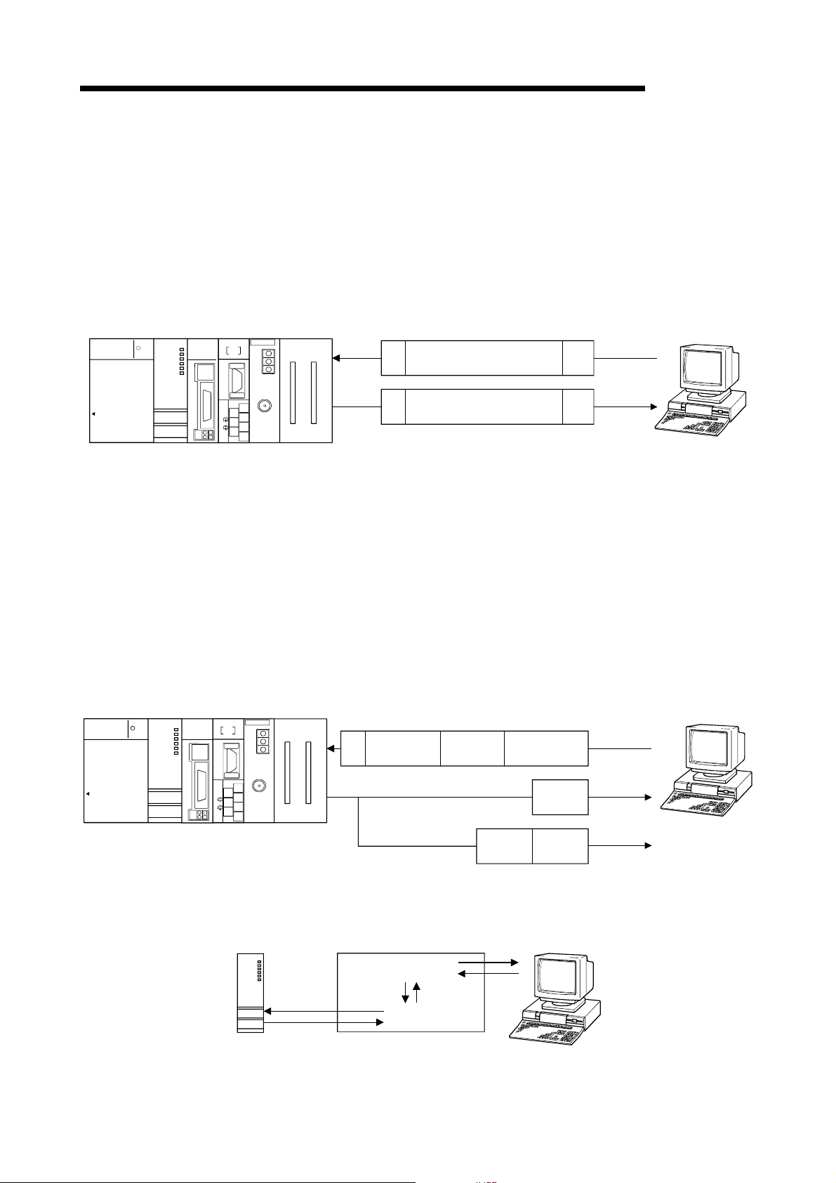
1 OVERVIEW
y
MELSEC-Q
(d) It is necessary to create a sequence program for communication control that
conforms to the external device.
(e) Communication can be performed using an user frame by registering the fixed
format portion of the head and tail sections of a message as an user frame.
• When sending data, the Q series C24 adds an user frame to any data
specified by the user.
• When receiving data, the Q series C24 transfers any data excluding the
user frame to the PLC CPU.
MELSEC
PULL
MELSEC
PULL
MITSUBISHI
MITSUBISHI
POWER
POWER
Q25HCPU
Q25HCPU
RS-232
RS-232
USB
QJ71E71
QJ71C24
RUN
ERR.
INIT.
MODE
COM.ERR
10BASE-T
CH2.CH1.
RD
CH1.
RS-232
CH.2
SDA
1
SG
2
SDB
(FG)
3
RDA
4
(FG)
5
RDB
6
RS-422
7
/485
STX
ETX
OPEN
RUN
SD
ERR.
USER
BAT.
BOOT
10BASE
USB
+12V
12G
When receiving data
Any data format
Any data format
When sending data
ETX
STX
(f) It is possible to clear the current reception data without interrupting the
transmission processing by using the dedicated instruction "CSET."
(3) Data communication using the bidir ectional pr otocol
(Details are explained in Chapter 7 and the User's Manual (Application).)
(a) In communication between PLC CPUs and communication with an external
device for which transmission/receive control programming is allowed, data
communication is performed in a sequence of "data transmission and
response receipt".
(b) Error check of received data can be performed using the sum-check code,
while the occurrence of a reception error at an external device can be
checked via an ACK/NAK response.
QJ71E71
QJ71C24
RUN
ERR.
INIT.
COM.ERR
MODE
RUN
ERR.
USER
BAT.
BOOT
CH1.
10BASE-T
CH2.
RD
CH1.
RS-232
CH.2
SDA
1
SG
2
SDB
(FG)
3
RDA
4
(FG)
5
RDB
6
RS-422
7
/485
ENQ
Data length
Sending completed normally
Any data
Sending completed
Error
code
Sum check
code
ACK
NAK
OPEN
SD
10BASE
+12V
12G
abnormall
(c) ASCII code data can be used for communication using the ASCII-BIN
conversion function.
QCPU
Q25HCPU
MODE
RUN
ERR.
USER
BAT.
BOOT
USB
RS-232
Binary
data
QJ71C24
ASCII-BIN
conversion
Binary
data
ASCII
data
1 - 4 1 - 4
Page 30
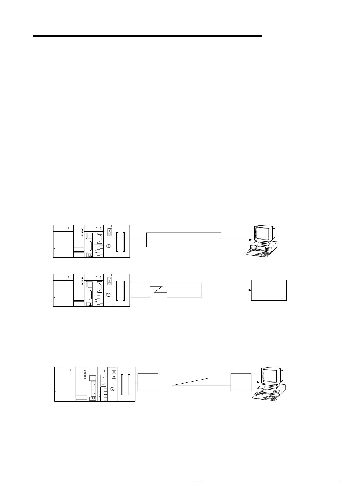
1 OVERVIEW
MELSEC-Q
(4) Monitoring the PLC CPU
(Details are explained in the User's Manual (Application).)
(a) The self-station's PLC CPU can be monitored at time intervals set by the
user without using a sequence program.
1) The following monitoring information can be sent/notified as the result of
monitori ng th e PL C CP U .
• Transmission of information on devices and the PLC CPU status to be
monitored. (It is also possible to send the monitoring information
through combined use of the modem function.)
• Notification of a notification message (string data) registered as the
connection data of the modem function, through combined use of the
modem function.
2) The user can select either one of the following timing choices at which to
send the PLC CPU monitoring result to the external device.
• Send/notify every time the PLC CPU is monitored (periodic
transmission).
• Send/notify when the information read from the PLC CPU matches
the conditions set by the user (conditional transmission).
MELSEC
MELSEC
PULL
PULL
MELSEC
MITSUBISHI
MITSUBISHI
PULL
MITSUBISHI
(b) The PLC CPU monitoring function can be used in communication using the
MC or non procedure protocol.
QJ71E71
Q25HCPU
POWER
RS-232
Q25HCPU
POWER
RS-232
QJ71C24
RUN
ERR.
MODE
INIT.
COM.ERR
CH2.CH1.
OPEN
RUN
SD
RD
ERR.
10BASE-T
10BASE
QJ71E71
OPEN
10BASE
CH1.
RS-232
CH.2
SDA
1
SG
2
SDB
(FG)
3
RDA
4
(FG)
5
RDB
+12V
6
12G
RS-422
7
/485
QJ71C24
RUN
ERR.
INIT.
COM.ERR
CH2.CH1.
SD
RD
10BASE-T
CH1.
RS-232
CH.2
SDA
1
SG
2
SDB
(FG)
3
RDA
4
(FG)
5
RDB
+12V
6
12G
RS-422
7
/485
Modem
Data
Notification
message
Pager
USER
BAT.
BOOT
USB
MODE
RUN
ERR.
USER
BAT.
BOOT
USB
(5) Remote communications using the modem function
(Details are explained in the User's Manual (Application).)
(a) Data communication can be performed with a remotely located external device.
(b) Modem initialization and line connection/disconnection can be performed.
(c) Data communication can be performed using the MC, non procedure or
bidirectional protocol.
QJ71E71
Q25HCPU
POWER
USB
RS-232
QJ71C24
RUN
ERR.
MODE
INIT.
COM.ERR
CH2.CH1.
OPEN
RUN
SD
RD
ERR.
USER
BAT.
BOOT
CH1.
10BASE-T
RS-232
10BASE
CH.2
SDA
1
SG
2
SDB
(FG)
3
RDA
4
(FG)
5
RDB
+
12V
6
12G
RS-422
7
/485
Modem Modem
(6) Initial settings and communication settings w ithout usi ng a
sequence program
Various initial settings can be performed using the GX Congifurator-SC
(SW0D5C-QSCU-E or later, hereinafter abbreviated as GX Configurator-SC).
1 - 5 1 - 5
Page 31

1 OVERVIEW
MELSEC-Q
(7) Connecting the GX Developer and the GOT
(a) Connecting the GX Developer (Details are explained in the GX Developer
Operating Manu al . )
• By connecting a PC installed with a GX Developer to the interface of the Q
series C24 at the same time, operations such as programming, monitoring
and testing for the PLC CPU can be performed.
• By connecting multiple PCs installed with GX Developers to the PLC CPU
or Q-series C24 at the same time, operations such as programming and
monitoring can be performed simultaneously by multiple operators.
Operating the GX Developers using these simultaneous connections can
improve program performance.
• Operations can be performed from a GX Developer by setting the
communication protocol of the Q series C24 interface to which a PC is
connected to "0" with the switch setting using the GX Developer.
(b) Connecting the GOT (Details are explained in the GOT User's Manual
(Connection).)
• By connecting a GOT (graphic operation terminal) to the interface for the
Q series C24 operations such as monitoring the PLC CPU can be
performed.
• Operations such as monitoring the PLC CPU can be performed by setting
the communication protocol of the Q series C24 interface to which a GOT
is connected to "0" with the switch setting using a GX Developer.
(c) Simultaneous connection of GX Developer and GOT
• It is possible to connect a PC with GX Develope r and the G OT to two
interfaces of the Q series C24 at the same time. It is thus possible for more
than one user to perform programming, monitoring, etc. simultaneously.
• When the GOT and the PC with GX Developer are connected at the same
time, the two interfaces of the Q series C24 cannot perform an interlock
operation.
Q25HCPU
RS-232
USB
MODE
USER
BOOT
RUN
ERR.
BAT.
QJ71C24-R2
CH1. CH2.
CH1.
CH2.
GX Developer
or
GX Developer
RS-232 cable
or
GOT
GOT
POINT
When GX Developer and/or the GOT is connected directly to the Q series C24,
switching settings using GX Developer need not be made to perform access to the
QCPU, monitoring and other operations. (They can also be performed when the
communication protocol is set to "0" by making switch settings using GX
Developer.)
1 - 6 1 - 6
Page 32

1 OVERVIEW
p
MELSEC-Q
(8) Functions supporting multiple CPU sy stems ( D etails are ex plai ned
in the Reference Manual.)
(a) When accessing QCPUs in a multiple CPU system using the MC protocol or
through GX Developer, it is possible to perform data communication such as
reading/writing device data by specifying the QCPU to be accessed.
• When using the Q series C24 in a multiple CPU system, a QCPU
controlling the Q series C24 (hereinafter referred to as the control PLC)
should be specified using GX Developer.
It is also possible to mount a Q series C24 of function version A in a
multiple CPU system and access to the only control PLC (PLC No.1).
External device
Peripheral device
Setting from
GX Developer
Q series C24
control PLC
1) 2) 3) 4)
Q series C24
non-control PLCs
1 2
1
C24
Communication through GX Developer
Communication using the MC protocol
1) : PLC No.1
2) : PLC No.2
3) : PLC No.3
4) : PLC No.4
: Module controlled by
1
PLC No.1
2
: Module controlled by
PLC No.2
(b) When a Q series C24 CPU of function version B is used in a multiple CPU
system, the following forms of data communication can be performed with
the Q series C24.
1) It is possible to perform data communication using the non
procedure/bidirectional protocols from the control PLC
2) It is possible to read the buffer memory from non-control PLCs.
Input/output signals can be used as contacts.
Non-control PLC
FROM
instruction
Use the input/
output signal as
a contact
Control PLC
FROM/TO instruction
Dedicated instruction
Use the input/
output signal as a
contact
It should be output
to an out
ut signal
Q series C24
Buffer memory
Data communication
X
Y
External
device
1 - 7 1 - 7
Page 33

1 OVERVIEW
g
r
MELSEC-Q
3) It is possible to access the control PLC and non-control PLCs using the
MC protocol and through GX Developer from the external device.
In addition, data communication with the control PLC of the Q series C24
can be performed using the non procedure/bidirectional protocol.
(Example) When communicating with the MC protocol
Non-control PLC
03E0H to 03E3
Data
Device memory, etc.
If the MC protocol, GX Developer is used to access other stations, it is
possible to access the control PLC and non-control PLCs of the station to
be accessed even if the relay station and the accessed station are
multiple CPU systems.
(Example)
It is possible to access other stations regardless
of whether the control PLC of the module to be
routed through is the same or diffe r ent.
Control PLC
H
03FF
Data
Device memory, etc.
Q series C24
Communication using the
MC protocol (read/write)
H
Specify the QCPU to be
accessed by the I/O number
of the requested module.
Command message
transmitted using a
QnA compatible 4C
frame
Response message
External device
External
device
Peripheral device
Setting from GX Developer
Relay station
Station to be accessed
The QnA compatible 4C frame should be performed for access to non-
control PLCs when communicating using the MC protocol.
However, the avail abl e fun cti ons differ depending on th e QCPU to b e
accessed (whether it is a control PLC or a non- control PLC ).
See the Reference Manual for the available fun ctions and a ccessible range.
A module used for routing can access the following modules when
accessing other stations:
• MELSECNET/H, MELSECNET/10 network module
• Q series C24 • Ethernet interface module
If there is a module of function version A among the modules for routing,
it is possible to access the control PLC of that particular module only. In
addition, it is possible to access other stations via a module controlled
by the same control PLC.
Local station
1) 2) 3) 4)
MELSECNET/H
2 21) 2) 3) 4)
MELSECNET/H
21) 2) 3) 4)
The modules used for the routing are MELSECNET/H network modules
1 2
1'
1) : PLC No.1
2) : PLC No.2
3) : PLC No.3
4) : PLC No.4
Communication throu
Communicatio n using the MC protocol
: Module used for routing, controlled
1
by PLC No.1
: Q series C24 controlled by
1'
PLC No.1
: Module used for routing, controlled
2
by PLC No.2
h GX Develope
1 - 8 1 - 8
Page 34

1 OVERVIEW
p
MELSEC-Q
(9) Remote password check function
(Details are explained in the User's Manual (Application ) and the R eference M anual.)
(a) The remote password check function of the Q series C24 prevents users at
a remote location to access QCPUs illegally using the modem function of the
Q series C24.
(The remote password is checked in the following forms of data communication)
• Communication using the MC protocol
(The remote password check is not carried out in data communication
using the non procedure/bidirectional protocols.)
• Access to th e PL C th ro ug h G X Dev eloper
The remote password function is one of the QCPU functions and used for
preventing illegal access to the QCPU by other users.
Use GX Developer to set a remote password for the QCPU in order to
activate the remote password function of the QCPU.
(b) If the Q series C24 is specified in the parameters of a QCPU as being
subject to the remote password check, the remote password can be
unlocked (canceled) using either one of the methods below, to allow data
communication from the external device. It is necessary to connect a line to
the modem first.
• When communicating using the MC protocol
Use the dedicated command for communication using the MC protocol to
unlock the remote password from the external device.
• When accessing the PLC through GX Developer
Unlock the remote password using GX Developer at the start of online
operation.
The remote password is automatically locked by disconnecting the line to
the modem.
Set the parameters to make
the Q series C24 as a subject to
the remote password check.
QCPU
Remote
password
GX Develo
er
Q series C24
Remote
password
check
Modem
Dialup line
Modem
Communication using the MC protocol
Communication through GX D ev e loper.
Accessing
external device
1 - 9 1 - 9
Page 35

1 OVERVIEW
1.3 About Added/Changed Functions in Function Versi on B
The table below lists the functions that have been added or changed in the Q series
C24 of function version B.
See Section 2.6 for the function version, serial NO. and software version of products
(CPU module, GX Developer, GX Configurator-SC) related to the Q series C24 which
can use added/changed functions.
See Appendix 1.1 concerning a comparison of functions in the different Q series C24
function versions.
Function
Simultaneous connection of
GX Developer and GO T
Control of RS and DTR
signal states
Support for 230 ,4 00 b ps
Data transmission/reception
at low speed
Clearing reception data by a
dedicated instruction
Transmission of the P LC
CPU monitoring information
through combined use of the
modem function
Remote passw ord che c k
Automatic initialization for
modem
Callback
Addition of non reception
monitoring time fo r ma t in
non procedure protocol
Transmission control
start/end fr ee area
designation
Addition of ch ang ea ble da ta
to the user frame
(05
, 0BH, 11H, 17H)
H
Addition of ch ang ea ble da ta
to the user frame
(04
, 0A
H
H, E5H, EBH
Adding a reception function
through the use of user
frames
)
QJ71C24N
(-R2/R4)
QJ71C24
(-R2)
Outline of function Reference section
This function allows access to the PLC from a PC with GX Developer and a
GOT connected to two different interfaces of the Q series C24 at the same
time.
This function allows the control of the on or of f sta te of th e R S and D TR
signals with the PLC program.
This function allows data communication with an external device at a
transmission speed of 230,400 bps.
This function allows data communication with an external device at a
transmission speed of 50 bps.
This function allows clearing reception data using the CSET instruction
during data co mmun i ca tion us ing th e no n pro ce du re prot oc o l.
It is possible to cl ea r th e da ta eve n when dat a i s be ing tr an s mi tte d.
When the PLC CPU monitoring function is active, this function sends the
monitoring information of the PLC CPU to the external device through the
modem.
This function allows data communication aft er the external device
completes the unlock processing of the remote password set at a QCPU. It
is executed whe n th e QC PU is a cce ss ed fro m a r e mote lo ca tio n us i ng the
modem functio n of the Q ser i es C24 in t he fo llow in g fo r ms of dat a
communication:
• Communication using the MC protocol
• Communication using GX Developer
Initializes the mode m au to mat ica l ly whe n Q Seri es C24 st ar t s up .
After line connection from the GX Developer, access to the QCPU from the
GX Developer i s made po s si b le thr oug h l ine re co nne c t ion from th e Q Ser ie s
C24 (callback). Transmission costs after line connection from the Q Series
C24 side are borne by the Q Series C24 side.
This function allow s me ss age s to be rec ei ved in th e no n re cep t ion pr ot oc ol
by time-out in non reception monitoring time (timer 0) if the received
complete c ode and received data count have been not determined.
This function al low s th e des ign at ion of th e av a ilab l e ca pa city of the OS area
that notifies th e da ta rece pt ion fa ilur e at t he ti me o f tran s mi ssi on con tro l
(DTR/DSR signal con tr ol and DC cod e c on tro l).
These functions allow the following codes to be registered as the
changeable da ta of user fra me s fo r da ta co mmun icat i on .
• Horizontal parity code
• Sum check code o f two ’ s- co mp le m en t nu mber
This function allows reception of a message consisting of the head frame
and any data field when receiving data by specifying the head frame.
The data length of the data field can be specified freely for each
combination of user frames for reception set by the user.
(Receiving 1 byte providing ACK/NAK only is also possible by setting the
data length of the data field to “0.”)
MELSEC-Q
Section 1.2 of
User’s Manual
(Basic)
Remark of se ct ion
3.2.1
Chapter 4 of
User’s Manual
(Basic)
Chapter 6, Section
9.8 of User’s
Manual (Basic)
Chapter 2 of
User’s Manual
(Application)
Chapter 3 of
User’s Manual
(Application)
Section 3.18 of
Reference Manual
Chapter 3 of the
User’s Manual
(Application)
Chapter 6 of
User’s Manual
(Application)
Chapter 7 of
User’s Manual
(Application)
Chapter 9 of
User’s Manual
(Application)
Chapter 11 of
User’s Manual
(Application)
1 - 10 1 - 10
Page 36

1 OVERVIEW
MELSEC-Q
Function
Multipl e specificatio n of
transparent codes for
transmission
Switchin g to th e GX
Developer co nne ct ion mode
by switching the mode
Communication data
monitoring function
UINI ins tr u c t io n
Support for multiple CPU
system
QJ71C24N
(-R2/R4)
QJ71C24
(-R2)
Outline of function Reference section
This function allows specification of a max imu m of 10 ty pe s of tra n sparen t
codes for transmission per interface when sending data using one of the
following proto co ls :
• Non procedure protocol
• Bidirectiona l pr otoc ol
This function s a l lows the GX De ve lo pe r co nne ct io n mode to be swi t che d by
an external device or the PLC CPU.
This function allows the monitoring of communication data transmitted on
the communication network of the Q series C24 and an external device.
The UINI instruction allows change of the mode, transmission specifications
and host station No. of the Q series C24.
This function allows access to the control/non-control PLCs specified by the
user when perfo r ming th e fo llow in g fo r ms of dat a co mmu ni cat i on wi th a
multiple CPU system:
• Communication using the MC protocol
• QCPU acces s fr o m GX Dev el op er
Chapter 12 of
User’s Manual
(Application)
Chapter 15 of
User’s Manual
(Application)
Section 3.13 of
Reference Manual
Chapter 16 of
User’s Manual
(Application)
Operating Manual
(Protocol FB
support function)
Chapter 17 of
User’s Manual
(Application)
Section 2.10 of
Reference Manual
1 - 11 1 - 11
Page 37

2 SYSTEM CONFIGURATION AND AVAILABLE FUNCTIONS
2 SYSTEM CONFIGURATION AND AVAILABLE FUNCTIONS
This Chapter describes the system configuration and available functions.
2.1 Applicable Systems
MELSEC-Q
The following describes applicable systems.
(1) Applicable modules and number of modules that can be mounted
The following table lists the CPU module and network modules (for remote I/O
stations) that the Q series C24 can be mounted and the number of modules
which can be mounted.
Applicable module
Q00JCPU Maximum 8
Q00CPU
Q01CPU
Q02CPU
CPU module
Network module
1 See User's Manual (Function Explanation, Program Fundamentals) for the CPU module to use.
2 See Q Corresponding MELSECNET/H Network System Reference Manual (Remote I/O
network).
Q02HCPU
Q06HCPU
Q12HCPU
Q25HCPU
Q12PHCPU
Q25PHCPU
QJ72LP25-25
QJ71LP25GE
QJ72BR15
Number of modules that
can be installed
Maximum 24
Maximum 64
Maximum 64
Maximum 64
Remarks
1
)
(
Can be installed in Q mode only
MELSECNET/H Remote I/O
(
(
station (
1
)
1
)
2
)
2
(2) The base module to which the Q ser i es C 24 can be mounted
The Q series C24 can be mounted into any I/O slot ( 1) of the base module.
1 Limited to within the range of I/O points for the CPU module and network
module (for remote I/O station)
(3) Multiple CPU systems
When using the Q series C24 on a multiple CPU system, refer to the QPU User's
Manual (Multiple CPU System) before operation.
(a) Applicable Q series C24
If using the Q series C24 on a multiple CPU system, use function version B
of the Q series C24.
(b) Intelligent function module parameter
To write the intelligent function module parameter on a PLC, be sure to
write it in the Q series C24 control PLC only.
2 - 1 2 - 1
Page 38

2 SYSTEM CONFIGURATION AND AVAILABLE FUNCTIONS
(4) Applicable software packages
(a) Software/setting & monitor tools ( 1) for the PLC
The following table lists the systems and software packages applicable for
the Q series C24.
When using the Q series C24, GX Developer is required.
2
Q00J/Q00/Q001CPU
Q02/Q02H/Q06H/
Q12H/Q25HCPU
Q12PH/Q25PHCPU
When installing an MELSECNET/H remote I/O
station
1 See section 2.6 for the versions of the GX Developer and GX Configurator-SC that support the
functions added through improvements in the Q series C24.
Single CPU system Version 7 or later
Multiple CPU system Version 8 or later
Single CPU system Version 4 or later SW0D5C-QSCU-E 00A or later
Multiple CPU system Version 6 or later SW0D5C-QSCU-E 20C or later
Single CPU system
Multiple CPU system
MELSEC-Q
Software packages
GX Developer GX Configurator-SC
Version 1.0 or later
(Versions prior to SW0D5C-
QSCU-E 40E are not usable.)
Version 7.10L or later
Version 6 or later SW0D5C-QSCU-E 30D or later
Version 1.13P or later
(Versions prior to SW0D5C-
QSCU-E 40E are not usable.)
(b) Communicati on sup po r t tools for external devi ce s
Item Name Model Remark
MX Component SWnD5C-ACT -E
1 Depending on the version of MX Component used, different versions of Q series C24 are
supported.
See the manual of MX Component for the details.
ActiveX control library.
The "n" in the model name is 0 or greater. (
1
)
2 - 2 2 - 2
Page 39

2 SYSTEM CONFIGURATION AND AVAILABLE FUNCTIONS
2.2 Combinations of PLC CPU and Ex ternal D evice, and Av ai l able Functi ons
The following describes the system configurations and available functions when using
the Q series C24.
(1) System configurations
System configurations (combinations of PLC CPU and external device) for data
communication are shown below.
(a) External device and Q series C24 with 1:1 system configuration
RS-232/422
QJ71E71
MELSEC
PULL
MITSUBISHI
Q25HCPU
POWER
USB
RS-232
QJ71C24
RUN
ERR.
MODE
INIT.
COM.ERR
OPEN
RUN
ERR.
USER
BAT.
BOOT
10BASE
CH2.CH1.
SD
RD
CH1.
10BASE-T
RS-232
CH.2
SDA
1
SG
2
SDB
(FG)
3
RDA
4
(FG)
5
RDB
+12V
6
12G
RS-422
7
/485
MELSEC-Q
(b) External device and Q series C24 with n:1 system configuration
RS-485
QJ71C24
QJ71E71
MELSEC
PULL
MITSUBISHI
Q25HCPU
RUN
RS-232
ERR.
MODE
INIT.
COM.ERR
OPEN
RUN
ERR.
USER
BAT.
BOOT
10BASE
USB
CH2.CH1.
SD
RD
CH1.
10BASE-T
RS-232
CH.2
SDA
1
SG
2
SDB
(FG)
3
RDA
4
(FG)
5
RDB
+12V
6
12G
RS-422
7
/485
POWER
2 - 3 2 - 3
Page 40

2 SYSTEM CONFIGURATION AND AVAILABLE FUNCTIONS
(c) External device and Q series C24 with 1:n system configuration
RS-485
MELSEC-Q
MELSEC
PULL
MITSUBISHI
ERR.
RUN
POWER
MODE
COM.ERR
INIT.
CH2.CH1.
OPEN
RUN
SD
RD
ERR.
10BASE-T
CH1.
USER
BAT.
BOOT
RS-232
10BASE
CH.2
SDA
1
SG
2
SDB
USB
(FG)
3
RDA
4
(FG)
5
RDB
+12V
RS-232
6
12G
RS-422
7
/485
MELSEC
POWER
PULL
MITSUBISHI
QJ71C24
QJ71E71
Q25HCPU
QJ71C24
QJ71E71
Q25HCPU
ERR.
RUN
MODE
COM.ERR
INIT.
CH2.CH1.
OPEN
RUN
SD
RD
ERR.
10BASE-T
CH1.
USER
BAT.
BOOT
RS-232
10BASE
CH.2
SDA
1
SG
2
SDB
USB
(FG)
3
RDA
4
(FG)
5
RDB
+12V
RS-232
6
12G
RS-422
7
/485
MELSEC
POWER
PULL
MITSUBISHI
QJ71C24
QJ71E71
Q25HCPU
ERR.
RUN
MODE
COM.ERR
INIT.
CH2.CH1.
OPEN
RUN
SD
RD
ERR.
10BASE-T
CH1.
USER
BAT.
BOOT
RS-232
10BASE
CH.2
SDA
1
SG
2
SDB
USB
(FG)
3
RDA
4
(FG)
5
RDB
+12V
RS-232
6
12G
RS-422
7
/485
MELSEC
POWER
PULL
MITSUBISHI
QJ71C24
QJ71E71
Q25HCPU
ERR.
RUN
MODE
COM.ERR
INIT.
CH2.CH1.
OPEN
RUN
SD
RD
ERR.
10BASE-T
CH1.
USER
BAT.
BOOT
RS-232
10BASE
CH.2
SDA
1
SG
2
SDB
USB
(FG)
3
RDA
4
(FG)
5
RDB
+12V
RS-232
6
12G
RS-422
7
/485
RS-485RS-232
QJ71E71
QJ71C24
Q25HCPU
MELSEC
PULL
MITSUBISHI
RUN
ERR.
POWER
INIT.
COM.ERR
MODE
CH2.CH1.
OPEN
RUN
SD
RD
ERR.
10BASE-T
CH1.
USER
BAT.
BOOT
RS-232
10BASE
CH.2
SDA
1
SG
2
SDB
USB
(FG)
3
RDA
4
(FG)
5
RDB
+12V
RS-232
6
12G
RS-422
7
/485
MELSEC
POWER
PULL
MITSUBISHI
QJ71C24QJ71E71
Q25HCPU
RUN
ERR.
INIT.
COM.ERR
MODE
CH2.CH1.
OPEN
RUN
SD
RD
ERR.
10BASE-T
CH1.
USER
BAT.
BOOT
RS-232
10BASE
CH.2
SDA
1
SG
2
SDB
USB
(FG)
3
RDA
4
(FG)
5
RDB
+12V
RS-232
6
12G
RS-422
7
/485
MELSEC
POWER
PULL
MITSUBISHI
QJ71C24QJ71E71
Q25HCPU
RUN
ERR.
INIT.
COM.ERR
MODE
CH2.CH1.
OPEN
RUN
SD
RD
ERR.
10BASE-T
CH1.
USER
BAT.
BOOT
RS-232
10BASE
CH.2
SDA
1
SG
2
SDB
USB
(FG)
3
RDA
4
(FG)
5
RDB
+12V
RS-232
6
12G
RS-422
7
/485
MELSEC
POWER
PULL
MITSUBISHI
QJ71C24QJ71E71
Q25HCPU
RUN
ERR.
INIT.
COM.ERR
MODE
CH2.CH1.
OPEN
RUN
SD
RD
ERR.
10BASE-T
CH1.
USER
BAT.
BOOT
RS-232
10BASE
CH.2
SDA
1
2
SDB
USB
(FG)
3
RDA
4
(FG)
5
RDB
+12V
RS-232
6
12G
RS-422
7
/485
(d) External device and Q series C24 with m:n system configuration
RS-485 RS-485 RS-485
QJ71E71
QJ71C24 QJ71E71
Q25HCPU
MELSEC
PULL
MITSUBISHI
RUN
ERR.
POWER
INIT.
COM.ERR
MODE
CH2.CH1.
OPEN
RUN
SD
RD
ERR.
10BASE-T
CH1.
USER
BAT.
BOOT
RS-232
10BASE
CH.2
SDA
1
SG
2
SDB
USB
(FG)
3
RDA
4
(FG)
5
RDB
+12V
RS-232
6
12G
RS-422
7
/485
MELSEC
POWER
PULL
MITSUBISHI
QJ71C24 QJ71E7 1
Q25HCPU
RUN
ERR.
INIT.
COM.ERR
MODE
CH2.CH1.
OPEN
RUN
SD
RD
ERR.
10BASE-T
USER
BAT.
BOOT
RS-232
10BASE
CH.2
SDA
1
SG
2
SDB
USB
(FG)
3
RDA
4
(FG)
5
RDB
+12V
RS-232
6
12G
RS-422
7
/485
MELSEC
PULL
MITSUBISHI
RUN
ERR.
POWER
INIT.
COM.ERR
MODE
CH2.CH1.
OPEN
RUN
SD
RD
ERR.
10BASE-T
CH1.
USER
BAT.
BOOT
RS-232
10BASE
CH.2
SDA
1
SG
2
SDB
USB
(FG)
3
RDA
4
(FG)
5
RDB
+12V
RS-232
6
12G
RS-422
7
/485
MELSEC
POWER
PULL
MITSUBISHI
QJ71C24 QJ71E71
Q25HCPU
QJ71C24
Q25HCPU
RUN
ERR.
INIT.
COM.ERR
MODE
CH2.CH1.
OPEN
RUN
SD
RD
ERR.
10BASE-T
CH1.
USER
BAT.
BOOT
RS-232
10BASE
CH.2
SDA
1
SG
2
SDB
USB
(FG)
3
RDA
4
(FG)
5
RDB
+12V
RS-232
6
12G
RS-422
7
/485
2 - 4 2 - 4
Page 41

2 SYSTEM CONFIGURATION AND AVAILABLE FUNCTIONS
(2) Correspondence between the data communic ati on functi ons and
system configurations
The following shows system configurations that can use the data communication
functions of the Q series C24.
The manual names shown in the reference section column in the table below are
as follows:
• Application
Q Corresponding Serial Communication Module User's Manual (Application)
• Reference
Q Corresponding MELSEC Communication Protocol Reference Manual
MELSEC-Q
(a) Communication using the MC protocol (
Functions of the Q series C24
PLC CPU device memory read/write Section 3.3
Intelligent function module buffer memory read/write Section 3.5
Sequence program read/write Section 3.8
PLC CPU status control (remote RUN, STOP, etc.) Section 3.6
On-demand function
Global function Section 3.10
Accessing the PLC of other stations in the MELSECNET/H,
MELSECNET/10
PLC CPU monitoring function Application Chapter 2
System configuration
1 : 1 n : 1 1 : n m : n
: Availabl e, : Not available)
Reference section
Reference
Section 3.11
Application Chapter 10
Reference
Section 2.7
(b) Communication using the non procedure protocol
(
: Available, : Not available)
Functions of the Q series C24
Data transmission/receiving in arbitrary format This manual Chapter 6
Data transmission/receiving with user frames Chapter 11
PLC CPU monitoring function Chapter 2
Reading received data using interrupt programs Chapter 4
Sending/receiving ASCII data using ASCII-BIN conversion
System configuration
1 : 1 n : 1 1 : n m : n
Reference section
Application
Chapter 13
(c) Communication using the bidirectional protocol
(
: Available , : Not available)
Functions of the Q series C24
Data transmission/receiving This manual Chapter 7
Reading received data using interrupt programs Chapter 4
Sending/receiving ASCII data using ASCII-BIN conversion
System configuration
1 : 1 n : 1 1 : n m : n
Application
Reference section
Chapter 13
In general, if data communication is performed using a system configuration of
other than 1:1 connection mode, the following points should be well noted.
• Avoid simultaneous transmission.
• Discard data received other than that addressed to the local station.
2 - 5 2 - 5
Page 42

2 SYSTEM CONFIGURATION AND AVAILABLE FUNCTIONS
r
r
2.3 For Use in Multiple CPU System
This section explains the use of the Q series C24 in a multiple CPU system.
(1) When making access from the external device to the non-control CPU of the Q
series C24 using either of the following functions, use the Q series C24 of function
version B.
When the Q series C24 of function version A is used, only the control CPU can be
accessed. (Access to the non -cont rol CPU will resul t in an error. )
• Communication using MC protocol
• Communication using GX Developer
External device
Multiple CPU system
Communication using MC protocol
Communication using GX Develope
MELSEC-Q
Q series C24 of function version B
(2) If the other stations to be accessed belong to the multiple CPU system, the
modules used for routing and QCPUs at the local station, all the relay stations,
and the accessed station should be modules of function version B or later. This
has to hold in all cases of accessing the non-control PLC of the module used for
routing and the accessed station.
1
(Example)
It is possible to access other stations regardless
of whether the control PLC of the module to be
routed through is the same or diffe rent.
Peripheral device
Setting from GX Developer
Relay station
Station to be accessed
Local station
1) 2) 3) 4)
MELSECNET/H
2 21) 2) 3) 4)
MELSECNET/H
21) 2) 3) 4)
The modules used for the routing are MELSECNET/H network modules
1 2
1'
1) : PLC No.1
2) : PLC No.2
3) : PLC No.3
4) : PLC No.4
1
1'
2
External device
Communication through GX Develope
Communication using the MC protocol
: Module used for routing, controlled
by PLC No.1
: Q series C24 controlled by
PLC No.1
: Module used for routing, controlled
by PLC No.2
1 When accessing other stations, a module used for routing can access the
following modules:
•
MELSECNET/H, MELSECNET/10 network modules
•
Q series C24
•
Ethernet interface modules
2 - 6 2 - 6
Page 43

2 SYSTEM CONFIGURATION AND AVAILABLE FUNCTIONS
2.4 For Use with Q00J/Q00/Q01CPU
This section describes the use of the Q series C24 with the Q00J/Q00/Q01CPU.
(1) Available functions
The following table indicates the functions that can be used when the Q series
C24 is mounted in the Q00J/Q00/Q01CPU.
Function Availability
Communications using the MC protocol (1)
Communications using non procedure protocol
Data reception by interrupt program
Communications using the bidirectional protocol
Data reception by interrupt program
Communications using dedicated instructions
Communications via public line, etc. (modem functi on)
Remote password check
Transmission
Control
Communications protocol switching
Independent/linked operation of each interface
Initial setting and monitoring/testing of setting values by the utility pac kage
Connecting the GX Developer and GOT
1 Communications are according to the MC protocol. See the Reference Manual concerning the
2 Use Q00J/Q00/Q01CPU (function version B) or later.
DC code control (including Xon/Xoff control)
DTR/DSR (ER/DR) control
number of devices that can be accessed and the processing time.
The range of devices that can be accessed differs depending on the frame used in data
communications.
When using the function, version 8 or later of the GX Developer is required.
MELSEC-Q
(2)
(2)
(2)
: Available : Not available
2 - 7 2 - 7
Page 44

2 SYSTEM CONFIGURATION AND AVAILABLE FUNCTIONS
2.5 For Use at MELSECNET/H Remote I/O Station
This section describes the use of the Q series C24 at a MELSECNET/H remote I/O
station.
It is not necessary to read this section if the Q series C24 is used with the QCPU.
(1) System configuration
(Example)
(Remote master station) (Remote I/O station)
QCPU
QJ71
LP21
-25
QJ72
LP25
-25
QJ71
C24
MELSEC-Q
MELSECNET/H
Remote I/O network
QJ72
LP25
-25
(Remote I/O station)
External device
(2) Available functions
The following table indicates the functions that can be used when the Q series
C24 is mounted on a MELSECNET/H remote I/O station.
Function Availability
Communications using the MC protocol
PLC CPU monitoring (PLC CPU monitoring function)
Communications using non procedure protocol
Data reception by interrupt program
PLC CPU monitoring (PLC CPU monitoring function)
Communications using the bidirectional protocol
Data reception by interrupt program
Communications using dedicated instructions
Communications via public line, etc. (modem functi on)
Remote password check
Transmission
Control
Communications protocol switching
Independent/linked operation of each interface
Initial setting and monitoring/testing of setting values by the utility pac kage (See (4))
Connecting the GX Developer
DC code control (including Xon/Xoff control)
DTR/DSR (ER/DR) control
: Available : Not available
(1)
(2)
(2)
(3)
(4)
2 - 8 2 - 8
Page 45

2 SYSTEM CONFIGURATION AND AVAILABLE FUNCTIONS
1 The following functions are available when communicating with the
MELSECNET/H remote I/O station using the MC protocol.
Available function Function
Batch read and batch write
Device memory read/write
Buffer memory read/write Reading/writing from/to the buffer memory of the Q series C24
Reading/writing buffer memory of an
intelligent function module
The following devices of a MELSECNET/H remote I/O station can be accessed
by the device memory read/write function. Note that the accessible devices and
the ranges vary depending on the type of frames used for the data
communication.
See the Refer e n ce Man ua l fo r a deta iled explanation.
Random read, test (random write)
Monitor data registration, monitoring
Batch read of multiple blocks, batch write of multiple bl ock s
Reading/writing from/to the buffer memory of the specified
intelligent function module
MELSEC-Q
Device name Device symbol Device name Device symbol
Special relay SM Link relay B
Special register SD Data register D
Input relay X Link register W
Output relay Y Link special relay SB
Internal relay M Link special register SW
REMARK
It is only possible to read/w rite from/to the buffe r memory of an inte lligent function
module for the MELSECNET/ 10 remote I/ O station co mpatible with th e QnA/A series.
2 PLC CPU monitoring can be registered using the MC protocol or GX
Configurator-SC.
The dedicated instruction CSET cannot be used for registration.
The device to be monitored can be registered within the device range of the
MELECNET/H remote I/O station.
2 - 9 2 - 9
Page 46

2 SYSTEM CONFIGURATION AND AVAILABLE FUNCTIONS
3 The dedicated instructions are unavailable for the MELSECNET/H remote I/O
station.
For the functions that use the dedicated instructions to make communication,
perform programming by the following methods.
Dedicated instruction Method Explanation section
FROM, TO Perform programming using the RE MFR/REMTO instruction. Appendix 9.2
ONDEMAND Appendix 9.3
INPUT Appendix 9.4
OUTPUT Appendix 9.5
BIDIN Appendix 9.4
BIDOUT
SPBUSY No method
CSET (Receive data clear)
BUFRCVS
PRR Appendix 9.7
CSET (Initial setting)
CSET (PLC CPU monitoring
function)
PUTE
GETE
UINI
Perform programming using the REMFR/REMTO instruction
and I/O signal.
Perform programming using the receive data clear request
area of the buffer memory.
No method
(Data cannot be received using an interrupt program)
Perform programming using the REMFR/REMTO instruction
and I/O signal.
No method
(Register/delete the PLC CPU using the MC protocol or GX
Configurator-SC.)
Perform programming using the REMFR/REMTO instruction
and I/O signal.
Perform programming using the REMFR/REMTO instructions
and I/O signals. (However, the station No. cannot be changed.)
MELSEC-Q
Appendix 9.5
Appendix 9.6
Appendix 9.8
Appendix 9.9
Appendix 9.11
Appendix 9.10
Appendix 9.12
4 Available for the MELSECNET/H remote I/O station of function version D or
later.
GX Developer Ve rsio n 8. 18 U o r lat e r i s requ i re d t o u se t he fu nc ti on .
2 - 10 2 - 10
Page 47

2 SYSTEM CONFIGURATION AND AVAILABLE FUNCTIONS
(3) Setting from GX Developer
The following parameters should be set through GX Developer in order to use
the Q series C24 mounted to a MELECNET/H remote I/O station.
Each of setting is the same way as when setting the parameters for the Q series
C24 mounted to a QCPU station: see Section 4.5 and after.
See the operating manual for GX Developer for how to display each setting
screen.
(Parameter setting items for the Q series C24 mounted to a MELECNET/H
remote I/O station)
Parameter setting item Setting Remarks
I/O Assignment Set the module mounting i nformation See Section 4.5.1
Switch setting for I/O and
intelligent function module
Remote password setting Perform settings for the remote password.
Set the transmission specification and the
communication protocol for communication
with the external device
MELSEC-Q
See Section 4.5.2
User's Manual (Application)
Section 3.3.3
POINT
(1) Connect GX Developer to a MELECNET/H remote I/O station and set the
parameters.
(2) Reset the MELECNET/H remote I/O station after changing the setting.
(4) When monitoring/setting with GX C onfig ur ator- SC
(a) About the automatic refresh setting
1) When reading/writing data created by the automatic refresh setting
using PLC, the read/write operation should be performed by GX
Developer. It cannot be performed from GX Configurator-SC.
2) The devices used for the automatic refresh setting must be of the types
M, B, D, or W.
POINT
(1) GX Configurator-SC should be connected to a MELECNET/H remote I/O
station before the monitoring/setting.
(2) The MELECNET/H remote I/O station should be reset after changing the
setting.
2 - 11 2 - 11
Page 48

2 SYSTEM CONFIGURATION AND AVAILABLE FUNCTIONS
MELSEC-Q
2.6 Checking the Function Version, Serial N o., and Softw are Ver si on
This section explains how to check the the function version, serial No. and software
version of related products that can use the functions added by the improvement of the
Q series C24.
(1) Correspondence of related products for use addi ti onal functions of
Q series C24
Additional function
Simultaneous connection of GX Developer and GOT Function version B
Transmission
specifications
Clearing reception data by a dedicated instruction Function version B
Communication
via modem
function
Non procedure and non reception monitoring time format
designation
Transmission con tro l st ar t/ en d fr ee area desi gna t ion Version 2 or later
Addition of
changeable da ta
to the user frame
Reception acc ord ing to us er fra mes
(reception according to format 1)
Multiple sp ec if ic at ion of tr an sp are n t co de s fo r
transmission
Switching the GX Developer connection mode by
switchin g th e mod e
Communication data monitoring function Version 8 or later Version 2 or later
UINI ins tr u c t io n
Remote passw ord che c k Function version B
RS and DTR signal status designation
Support for 23040 0 bp s
Data transmission/ reception at low
speed (50 bps)
Transmission of the P LC C PU
monitoring information through
combined use of the mode m fu nct io n
Automation initialization of modem
Callback
05H, 0BH, 11H, 17
04H, 0A
, EB
E5
H
H
H
H
Function version of the Q series C24 Version of related product
QJ71C24N
(-R2/R4)
Function version B
or later whose first
5 digits of the serial
No. are 06062
Function version B
or later whose first
5 digits of the serial
No. are 06062
QJ71C24 (-R2) CPU module GX Developer
Function version B
Function version B
Function version B
or later whose first
5 digits of the serial
No. are 03043
Function version B
Function version B
Function version B
Function version A
or later whose first
5 digits of the serial
No. are 02092
Version 7 or later
Version 6 or later
: Usable (no restrictions depending on the version) : Not usable
GX Configurat or-
SC
Version 2 or later
SW0D5C-QSCU-E
20C or later
Version 1.0 or later
(Versions prior to
SW0D5C-QSCU-E
40E are not
usable.)
Version 2 or later
SW0D5C-QSCU
20C or later
Version 2 or later
Version 2.06G or
later
SW0D5C-QSCU-E
20C or later
SW0D5C-QSCU-E
20C or later
SW0D5C-QSCU-E
20C or later
(2) Checking the version and serial No. of Q series PLC functions
(a) Using the rated plate on the side of the module to check
The serial No. and function version of the corresponding module is shown in
the SERIAL column of the rated plate.
Serial No . (first 5 digits)
Function version
Compliant standard
2 - 12 2 - 12
Page 49

2 SYSTEM CONFIGURATION AND AVAILABLE FUNCTIONS
(b) Using the GX Developer to check
The method of checking the serial No. and function version of the
corresponding module with the GX Developer is shown.
The serial No. and function version are displayed on the GX Developer
"Product Information List" or "Module's Detailed Information" screen.
The method of checking the serial No. and function version on the "Product
Information Li st" screen is sh own below. (See Section 10. 1. 1 fo r de t ail s
about the "Module's Detailed Information" screen.)
[Start Procedure]
"Diagnostics" "System monitor" "Product Inf. List"
MELSEC-Q
[Serial No., Ver.]
• The corresponding module's serial No. is shown in the Serial No. column.
• The function version of the corresponding module is shown in the Ver. column.
(3) Checking the software version of the GX Configur ator - SC
The GX Configurator-SC software version can be checked on the "Product
Information List" screen of the GX Developer.
[Start Procedure]
"Help" Product Information
Software version
2 - 13 2 - 13
Page 50

2 SYSTEM CONFIGURATION AND AVAILABLE FUNCTIONS
REMARK
The version indication for the GX Configurator-SC has been changed as shown
below from the SW0D5C-QSCU-E 40E upgrade product.
Previous product Upgrade and subsequent versions
SW0D5C-QSCU-E 40E
GX Configurator-SC Version 1.10L
MELSEC-Q
2 - 14 2 - 14
Page 51

3 SPECIFICATIONS
3 SPECIFICATIONS
The following shows the Q series C24 performance specifications.
See the User's Manual of the QCPU (Q mode) for general specifications.
3.1 Performance Specifications
The following shows the Q series C24 performance specifications. For the
transmission specifications when communicating via the modem function, see this
section and Chapter 3 of User's Manual (Application).
(1) Transmission specification
Specifications
Item
CH1
Interface
CH2
Line Full-duplex/half-duplex communications
MC protocols
Communication s
system (
Synchronizat ion met hod Start-stop sy nchr on iza ti on met hod
Transmission speed
Data format
Access cycle
Error detecti on
1)
communication
Non procedure protocol
communication
Bidirectional protocol
communication
[QJ71C24N(-R2/R4)]
• Transmission speed 230400 bps is available for only CH1. (Not available for CH2)
• Total transmission speed of two interfaces is available up to 230400 bps.
• Total transmission speed of two interfaces is available up to 115200 bps when the communication data
[QJ71C24(-R2)]
• Total transmission speed of two interfaces is available up to 115200 bps.
Start bits 1
Data bits 7/8
Parity bits 1 (vertical parity) or none
Stop bits 1/2
MC protocol communication
Non procedure protocol
communication
Bidirectional protocol
communication
Parity check All protocols and when ODD/EVEN is selected by parameter.
Sum check code
Processes one requ es t du r ing in st a lled PL C CPU END proces s ing .
Sends each time a send request is issued. Can receive at any time.
MC protocol/b id irec t io na l prot oc o l sel ec ted by par a mete r.
Non procedure protocol selected by user frame.
QJ71C24N
QJ71C24
RS-232-complia nce
(D-sub 9 pin)
RS-422/485-compliance
(2-piece terminal block)
Full-duplex/full-duplex communications
Full-duplex/full-duplex communications
50 300 600 1200 2400 4800 9600
14400 19200 28800 38400 57600 115200 230400 (bps)
monitoring function is used.
50 300 600 1200 2400 4800 9600
14400 19200 28800 38400 57600 115200 - (bps)
Number of scans tha t mu st be pr oc esse d/ nu mbe r of l ink s can s depe nd s on the con te nt s of th e req ue st .
(See Reference Manual.)
QJ71C24N-R2
QJ71C24-R2
RS-232-complia nce
(D-sub 9 pin)
RS-232-complia nce
(D-sub 9 pin)
Half-duplex communications
MELSEC-Q
3
QJ71C24N-R4
RS-422/485-compliance
(2-piece plug-in connector socket
block)
RS-422/485-compliance
(2-piece plug-in connector socket
block)
(Continued on next page)
3 - 1 3 - 1
Page 52

3 SPECIFICATIONS
(Continued from preceding page)
Specifications
Item
Transmission control
Line configuration
3
(Connection) (
Line configuration
(Data
communication)
(
2)
Transmission
distance (Overall
distance)
Flash ROM write count Maximum 100,000 times to the same area
Number of occupied I/O points 32 points per slot (I/O assignment: Intelli: 32 points) ( 3)
Recommended
cable
Applicable connector for external wiring D-sub 9 pin (male) screw type ( 5) —
5V DC internal current consumption 0.31A 0.26A 0.39A
External dimensions 98 (3.86 in.) (H) 27.4 (1.08 in.) (W) 90 (3.54 in.) (D )[ mm]
Weight 0.20kg (0.44lb)
RS-232 1:1 1:1 —
2)
RS-422/485 1:1, 1:n, n:1, m:n — 1:1, 1:n, n:1, m:n
MC protocols
communication
Non procedure
protocol
RS-
communication
232
Bidirectional
protocols
communication
MC protocols
communication
Non procedure
RS-
protocol
422/
communication
485
Bidirectional
protocols
communication
RS-232
RS-422/485
RS-232
RS-422/485
7/0. 127
(Oki Electric Cable Co., Ltd. Applicable number is specified in
SPEV (SB)-MPC-0.2 3P Outside diameter approx. 6.5mm (0.26 in.) (Mitsubishi Cable Industries, LTD.)
SPEV(SB)-0.2
1 Set to transfer data with external devices using a full-duplex communication system when the Q series C24
is started. For switching to a half-duplex communication system, refer to the User’s Manual (Application).
2 Indicates possible combinations when connecting the PLC CPU and external devices (external device
side: PLC CPU side). The total number of n and m+n is up to 32 stations.
3 In order to use the Q series C24, it is necessary to set the GX Developer switches.
To set the GX Developer switches, refer to section 4.5.
4 Recommended cables SPEV (SB)-MPC-0.2 3P and SPEV (SB)-0.2 3P are equivalent in the electrical
characteristics, but partially different in the outside diameter, internal wire colors, etc.
5 See Section 3.2.1 (3) for the recommended connector.
QJ71C24N
QJ71C24
DTR/DSR (ER/DR) control Enabled Disabled
RS/CS control Enabled Disabled
CD signal control Enabled Disabled
DC1/DC3 (Xon/Xoff) control
DC2/DC4 control
• DTR/DSR sign al con t ro l an d DC co de con tr ol are se le cted by the user .
1:1, 1:n, m:n 1:1
1:1, 1:n, n:1 1:1
1:1 1:1
1:1, 1:n, m:n 1:1, 1:n, m:n
1:1, 1:n, n:1 1:1, 1:n, n:1
1:1
Maximum 15 m
(49.2 ft.)
Maximum 1200 m (4592.4 ft.)
(overall distance)
P HRV-SV Outside diameter 8.5mm (0.33in.) or more
3P Outside diameter approx. 7.5mm (0.3 in.) (Mitsubishi Cable Industries, LTD.) ( 4)
QJ71C24N-R2
QJ71C24-R2
RS-232 RS-422/485
Enabled Enabled
—
Maximum 15 m
(49.2 ft.)
—
.)
MELSEC-Q
QJ71C24N-R4
—
1:1
—
Maximum 1200 m (4592.4 ft.)
(overall distance)
3 - 2 3 - 2
Page 53

3 SPECIFICATIONS
3.2 RS-232 Interface Specification
The following shows the RS-232 interface specifications.
3.2.1 RS-232 connector specifications
The following shows the specifications of the RS-232 connector that connects the Q
series C24 to an external device.
MELSEC-Q
1
2
3
4
5
Full-duplex
communication
Half-duplex
communication
Signal direction
C24
External
device
6
7
8
9
Pin number
1
2
3
4
5
6
7
8
9
Signal
abbreviation
CD
RD(RXD)
SD(TXD)
DTR(ER)
SG
DSR(DR)
RS(RTS)
CS(CTS)
RI(CI)
Signal name
Carrier detect
Receive data
Send data
Data terminal ready
Signal ground
Dataset ready
Request to send
Clear to send
Call Indicate
(1) The control signals are described below. (The pin numbers of the connector are
enclosed in parentheses.)
1) CD signal (1 )
• The Q series C24 operates according to the setting CD terminal check (see
Section 8.4.5) of the Q series C24.
CD terminal check enabled CD terminal check disabled
• The Q series C24 performs send and receive
processing when the CD signal (receive
carrier detection) is ON.
• If the CD signal is turned off during data
communication, the Q series C24 initializes
the transmission sequence.
See Chapter 8 of User's Manual (Application) Setting impossible.
• The Q series C24 performs send and receive
processing regardless of the ON/OFF status
of the CD signal.
• Data communications is possible with an
external device that cannot turn the CD
signal ON/OFF.
2) RD signal
This is a signal to receive data.
3) SD signal
This is a signal to send data.
3 - 3 3 - 3
Page 54

3 SPECIFICATIONS
MELSEC-Q
4) DTR signal (4)
• When communicating data using the non procedure protocol, the Q series
C24 turns on or off (on when data is receivable) depending on the amount
of unused memory in the OS area allocated for receive data storage, if
DTR/DSR control is being performed.
Read the receive data from the sequence program, as the receive data is
stored in the OS area when the DTR signal is OFF.
If DTR/DSR control is not implements, the DTR signal is always ON.
• If an MC protocol or bidirectional protocol is performing data communication,
the Q series C24 tu rn s ON when communications is enab led.
5) DSR signal (6)
• During DTR/DSR control, if this signal is OFF, the Q series C24 does not
send data to th e e xte r nal de vi ce.
Be sure that this signal is always turned ON when the external device is
ready to receive.
• If DTR/DSR control is not implemented, the DSR signal status is ignored.
6) RS signal (7)
• The Q series C24 turns ON/OFF the RS signal as shown below.
• When the communication system is full-duplex communications, if the Q series
C24 ready signal (X1E) i s ON, the Q serie s C24 tu rns ON t he RS signal .
• When the communication system is half-duplex communications, when the
Q series C24 send s data to an e xte rnal devi ce , it tu rn s ON th e RS si gn al .
• The RS signal is no t tu rne d OF F ev en whe n the receive data cannot be
stored in the Q series C24.
7) CS signal (8)
• The Q series C24 does not send data to an external device when this signal is OFF.
• Be sure that thi s sign al is always turned ON when the exter na l de vi ce is
ready to receive.
8) RI signal (9 )
• The RI signal is used when the modem status is monitored on the Q series
C24 side. It should be connected as needed. The RI signal is not needed
to be connected when the modem is not connected.
(2) The ON and OFF states of each signal indicate the following conditions:
(Output side) (Input side)
………
ON
………
OFF
(3) Interface connector
The Q series C24 uses the following type of RS-232 interface connector.
9-pin D sub (female) screw fixing type
Use one of the following as a connector shell for the connection cable of
the Q series C24 side.
• 3M
Plug model: 8209-6009 Shell model: 3702-2209 M2.6
• Tyco Electronics AMP K.K.
Plug model: 747904-2 Shell model: 747515 or 174469-2
5 V DC to 15 V DC, 3 V DC to 15 V DC
–5 V DC to –15 V DC, –3 V DC to –15 V DC
3 - 4 3 - 4
Page 55

3 SPECIFICATIONS
Buffer memory address 92
MELSEC-Q
REMARK
(1) Confirmation of RS-232 control sig nal status
The control signal status of DTR, DSR, RS, and CD can be confirmed during
data communication by the RS-232 control signal status storage area (address
H
254
, 264H) of the GX Configurator-SC or Q series C24 buffer memory.
Buffer memory address
CH1 side CH2 sideBit position
254
H
b0 RS
b1 DSR
b2 DTR
b3 CD
b4
b5 RI
b6 to b15 —
1 System area for QJ71C24 (-R2)
CS
1
(2) Designation of RS and DTR signal status
When the Q series it turned on or off, the on and off states of the RS and DTR
signals can be designated when the buffer memory of the RS and DTR signal
status designation area (address: 92
on or off by the RS signal or DTR signal.
b15 b3 b2 b1 b0
/132
H
H
H
, 132H) for the correspond in g bi t is tur ned
1 2 3
1/0
264
1/0
[Default 0005
H
H
]
1 The RS signal is controlled by the Q series C24 in the following cases. (Ignore setting
contents.)
• When data is communicated with half-duplex communication
• When communication time and the RS and CS signals are controlled by the modem function
2 The DTR signal is controlled by the Q series C24 in the following cases. (Ignore setting
contents.)
• When the DTR and DSR signals are controlled
• When data is communicated by the modem function
3 After writing in the buffer memory, a lag of 0 to 20 ms occurs until it is reflected in the signal.
POINT
Be sure to control the RS and DTR signals with the Q series C24. Control of the RS
and DTR signals by the user is a prime factor for data communication errors.
3.2.2 RS-232 cable specification
• Use a 15 m (49.21 ft.), or shorter, cable conforming to the RS-232 standard as the
RS-232 cable.
(Recommended cable)
7/0. 127
13P HRV-SV)
(Oki Electric Cable Co., Ltd)
System
RS
DTR
1:ON
0:OFF
P HRV-SV… : Designates the number of pairs. (For 13 pairs 7/0.127
3 - 5 3 - 5
Page 56
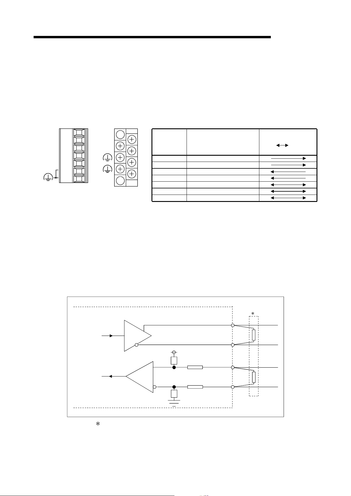
3 SPECIFICATIONS
3.3 RS-422/485 Interface Specifications
The following shows the RS-422/485 interface specification.
3.3.1 RS-422/485 terminal block specifications
The following shows the specifications of the RS-422 connector and RS-422/485
terminal block that connect to an external device.
SDA
Signal
abbreviation
SDA
SDB
RDA
RDB
SG
FG
FG
(FG)
SDB
RDA
RDB
SG
QJ71C24N-R4
(FG)
(FG)
SG
SDA
SDB
RDA
RDB
QJ71C24N
QJ71C24
Signal name
Send data (+)
Send data (–)
Receive data (+)
Receive data (–)
Signal ground
Frame ground
Frame ground
MELSEC-Q
Signal direction
C24
External
device
Send data
Receive data
(1) The following describes the control signals.
1) SDA, SDB signals
These are signals to send data from the Q series C24 to the external
device.
2) RDA, RDB signals
These are signals for the Q series C24 to receive data from the external
device.
(2) The following shows the function block diagrams.
(RS-422/48 5 inte r fa ce )
+
–
+
–
1
SDA
SDB
RDA
RDB
1 The following shows the terminal resistor connection.
Connect the terminal resistor according to Section 4.4.2 or the User's Manual
(Hardware) of the Q series C24 used.
3 - 6 3 - 6
Page 57

3 SPECIFICATIONS
3.3.2 RS-422/485 cable specifications
The following sh ow s the RS-422/485 cable speci fi cat ion.
(1) Use a 1200 m (3937 ft.), or shorter, cable that satisfies the following specification
for the RS-422/485 cable (cable to connect the Q series C24 terminal block).
(2) Make the tot al dist an ce wit hin 12 00 m (393 7 ft .) wh en tw o o r more devi ce ar e
connected in a 1:n or m:n configuration.
(3) The RS-422/485 cable specification is shown below.
Item Description
Cable type Shielded cable
Number of pairs 3P
Conductor resistance (20 C°)
Insulation resistance
Dielectric strength 500 V DC, 1 minute
Electrostatic capacitance (1 kHz) 60nF/km or less on average
Characteristic impedance (100 kHz)
88.0
10000 M
110 ± 10
MELSEC-Q
/km or less
- km or more
(Recommended cable)
SPEV (SB)-MPC-0.2
SPEV (SB)-0.2
3P
3P
..............
.....
(MITSUBISHI CABLE INDUSTRIES, Ltd.)
(MITSUBISHI CABLE INDUSTRIES, Ltd.)
SPEV (SB)-MPC-0.2 3P and SPEV (SB)-0.2 3P have the same electrical
characteristics, but different external diameter and internal wire colors.
3 - 7 3 - 7
Page 58

3 SPECIFICATIONS
3.3.3 Precautions when transferring data using R S- 422/485 cir c uit
The following precautions must be observed when transferring data with an external
device through the Q series C24 RS-422/485 interface.
Take the fo llowing into account when th e t r an sfe r rin g dat a wi th th e e x te rna l dev i ce .
(1) Error receive data countermeasures at external device during RS-
422/485 connection
If the external device may receive erroneous data, install a pull-up or pull-down
resistor to th e e xte rnal device as follows.
Installing a pull-up or pull-down resistor (resistance value criteria: approx. 4.7 k
1/4 W) can preven t the r e cept ion o f e rro ne ou s data .
4.7kΩ 1/4W
RDA
RDB
Terminating
resistor
4.7kΩ 1/4W
+
-
Receive data
MELSEC-Q
External device
POINT
When there is a pull-up or pull-down resistor at the external device, erroneous data
is not received .
REMARK
The following de scri be s th e ca se when a pu ll -up or pull - d own r esi st or i s not in stal le d
to the exter nal devi ce .
When no station is sending, the send line becomes high impedance and noise, etc.
may cause the send line to change and the external device to receive erroneous
data.
In this case, there is probably a parity error or framing error.
Therefore, skip the erroneous data.
Since the fir st da ta du ring d ata re cept io n i s fi xe d in the fo llow i ng ca ses, al so skip t he
receive data until the fixed head data is received.
• When using an MC protocol to send data, the first data is fixed according to the
frame and format the user uses.
• When transferring data using user frames with non procedure protocol or
bidirectional protocol, the first data is selected according to the user frame that the
user registers to the Q series C24.
3 - 8 3 - 8
Page 59

3 SPECIFICATIONS
(2) RS-422/485 interface operation
MELSEC-Q
1) RS-422-485 interface construction
The following illustration shows the construction of the Q series C24 RS422/485 interface driver (send)/receiver (receive).
SDR
SDB
RDA
RDB
Driver
Send data
Output control input ( 1)
Receiver
Receive data
1 "Output cont rol in pu t" (al so called send gate) of
the driver (send) section of the illustration at
the left dete rmi ne s wh ethe r o r not dat a fro m
SDA/SDB is output to the outside.
2) RS-422/485 interface operation
When the "Output control input" in the illustration above is ON, the interface
enters the low impedance state (state in which data can be sent).
When the "Output control input" is OFF, the interface enters the high
impedance state (state in which data cannot be sent).
3) Timing to start sending and to complete the transmission processing for the Q
series C24
• Timing to start sending
During data transmission, the Q series C24 outputs the actual data after
sending a mark for 2 characters, or longer, after the high impedance set by
the operations described in 1) and 2) above is reset.
• Transmission processing completion timing
The following times are necessary as H/W gate OFF time from the time that
data transmission is completed until transmission processing is completed
(the state changes to the high impedance state). (The transmission rate set
in the Q Series C24 is the object.)
When the transmission rate
is 600 bps or high e r
: Time for 0 to 1 bits of data to be sent
When the transmission rate
is 50 bps, 300 bp s : several ms
(Output control input)
External device
Q series C24
(Output control input)
Data
Outputs a mark for 2 characters, or longer
Data send time range
"Output control input"
ON time range
(Low impedance state)
Q series C24 is in the data
transmission and data
reception enable status
H/W gate OFF time
(See explanation above)
Q series C24 is in the data
Data
"Output control input"
OFF time range
(High impedance state)
reception enable state.
3 - 9 3 - 9
Page 60

3 SPECIFICATIONS
POINT
(1) When the external device and the Q series C24 connected in n:1 and m:n configurations
When the send signal of each device is connected as shown below, if the "Output control input" is
turned ON at two or more devices, the relevant devices output (send) data at the same time.
For the external device to transfer data normally,
• "Output control input" must be turned ON only when sending data.
• "Output cont rol i npu t" must be tu rned OFF when no t send in g data .
External device or converter
Send data
Output control input
Receive
data
SDA
SDB
RDA
RDB
SDA
SDB
Output control input
RDA
RDB
Send data
Q series C24
Receive
data
MELSEC-Q
SDA
SDB
Output control input
RDA
RDB
Send data
Q series C24
Receive
data
(2) When the Q series C24 is used, if operation of the two interfaces is linked (see Section 4.5.2 (2)), the
time to send one character becomes the Q series C24 H/W gate OFF time.
(The Q series C24 turns OFF the gate after the one-character send time.)
3 - 10 3 - 10
Page 61

3 SPECIFICATIONS
MELSEC-Q
3.4 Serial Communication Module Function List
The following table lists the functions of the Q series C24.
Function Reference section
Communication with QnA compatible 3C frame
Communication with
ASCII code
Communication with
binary code
Communication
using MC protocol
(
1)
Communication
using non
procedure protocol
(
2)
Communication
using bidirectional
protocol (
Communication via
public network, etc.
(modem function)
Transmission
control
Independent/linked operation of each interface Section 4.5.2
Monitoring/testing of initial settings and setting values with utility software Chapter 8
Supporting multiple CPU system
Remote password check
1)
Read/write of device
memory
Reading/writing from/to the buffer memory of the Q series C24
Reading/writing from/to the buffer memory of intelligent function modules
Reading/writing from/to sequence program files
Monitoring the PLC CPUs (PLC CPU monitoring function)
Status control of the PLC CPUs (remote RUN/STOP, etc.)
Turning on/off input signals of the Q series C24 from an external device (global function)
Data transmission from a PLC CPU to an external device (on-demand function)
Data transmission/reception in any format Chapter 6
Data transmission/reception using user frames
Data reception by interrupt programs
Monitoring the PLC CPUs (PLC CPU monitoring function)
ASCII data transmission/reception by ASCII-BIN conversion
Data transmission/reception by specifying transparent code
Data transmission/reception in any format Chapter 7
Data reception by interrupt programs
ASCII data transmission/reception by ASCII-BIN conversion
Data transmission/reception by specifying transparent code
Communication with MC Protocol/non procedure protocol/bidirectional protocol
PLC access fro m GX Developer
DC code control (including Xon/Xoff control)
DTR/DSR (ER/DR) control
1 If the external device is capable of incorporating a program and communicating
data using a protocol of the MELSEC PLC, it is possible to access the PLC CPU
using the above mentioned MC protocol. Furthermore, it is possible to transfer any
data using the bidirectional protocol.
2 When it is necessary to communicate using the protocol of an external device,
such as a measuring instrument or a bar code reader, the above-mentioned non
procedure protocol is used for data communication. In that case, the processing of
the communication data becomes easier by using the user frame communication
function.
Communication with QnA compatible 4C frame
Communication with QnA compatible 2C frame
Communication with A compatible 1C frame
Communication with QnA compatible 4C frame Format 5
Batch read/write in bit/word units
Monitoring of device memory
Batch read/write of multiple blocks
Read/write by extension designation
Accessing other stations via network system
Formats 1 to 4
exist for each.
Chapter 5
Reference Manual
User's Manual
(Application)
User's Manual
(Application)
Section 2.10 of
Reference Manual
Section 3.3.3 of
User's Manual
(Application)
3 - 11 3 - 11
Page 62

3 SPECIFICATIONS
3.5 Dedicated Instruction List
The following table lists dedicated instructions that can be used in the Q series C24.
MELSEC-Q
: Available : Not available
Classification Instruction Description
ONDEMAND Sends data with the on-demand function
OUTPUT Sends designated number of data
INPUT Receives data (reads received data)
BIDOUT Sends data
BIDIN Receives data (reads received data)
Reads the status of data sent/received with each
dedicated instruction
Allows clearing data received up to the present
without interrupting the data transmission
processing.
Receives data with an interrupt program (reads
received data)
Sends data with user frames using transmission
schedule table
Stores user frames in flash ROM of the Q series
C24 (writing)
Reads user frames stored in flash ROM of the Q
series C24
Performs PLC CPU monitoring
registration
Cancels PLC CPU monitoring
Sets the unit for the number of communication
data (words/bytes) and the data communication
area
Changes the mode, transmission specifications
and host station No. of the Q series C24.
For data
communication
Setting value
registration/
reading
PLC CPU
monitoring
instructions
Initial value
setting
instruction
Mode switching
instruction
SPBUSY
CSET
BUFRCVS
PRR
PUTE
GETE
CSET
UINI
For PLC
CPU
monitoring
function
Protocol
MC Non Bi
Abbreviations used in the
Protocol colu mn
MC : MC protocol
Non : Non procedure
protocol
Bi : Bidirectional protocol
Reference
section
Chapter 9
Chapter 17 of
User's Manual
(Application )
3 - 12 3 - 12
Page 63

3 SPECIFICATIONS
MELSEC-Q
3.6 Utility Package (GX Configurator-SC) Function List
The following t abl e list s th e utility package function for th e Q serie s C2 4.
(
: Protocol for which setting is valid)
Non-
Function MC
Auto ref resh setting
User frame Register the user frame in the flash ROM. — Section 8.4.1
Data for modem initialization Register the data for modem initialization in the flash ROM. Section 8.4.2
Data for modem connection Register the data for model connection in the flash ROM. Section 8.4.3
Modem functio n sy ste m
setting
CHn Transmission
control and other s
system se tt in g
CHn MC protocol
system se tt in g
CHn Non procedure
system se tt in g
System
CHn Bidirectional
setting
system se tt in g
CHn PLC CPU
monitoring system
setting
CHn Transmission
user frame No.
designation system
setting
System setting default
System setting write Write the setting values in the buffer memory to the flash ROM. Section 8.4.11
Flash ROM write
allow/prohibit designation
X · Y monitor/tes t Perform the mon itor i ng /tes t in g of I/ O s igna ls to /fro m the PL C CPU . Section 8.6.1
Modem function monitor/test Monitor the execution status of the modem function. Section 8.6.2
CHn Transmission
control and other s
monitor/test
CHn MC protocol
monitor
CHn Non procedure
monitor/test
Monitor
CHn Bidirectional
monitor
CHn PLC CPU
monitoring monito r
CHn User frame
No. designati on
monitor for
transmission
Monitor/test others Monitor the data reception result, error occurrence status, etc. Section 8.6.9
ERR LED off Turn off the ERR LEDs on the front face of the module. Section 8.6.10
Non procedure protocol
receive data clea r
Refresh the Q se r ie s C24 's erro r co de s and se t de vi ce s on the PLC
CPU side.
Register the system setting values for model function in the flash
ROM.
Set the tr ansmission specif ications with the other device.
(DTR/DSR control, DC code control, communication method, data
communication monitoring timer value, etc.)
Assign the buffer memory for on-demand function, set the user
frame number, etc.
Assign the buffer memory needed to perform data communication
using the non procedure protocol, and change the setting values,
etc.
Assign the buffer memory needed to perform data communication
using the bidirectional protocol, and change the setting values, etc.
Set the PLC CPU monitoring function.
Set the user frame number to be transmitted, etc. —
Reset the set t ing va lu es in the bu ffe r me mory to the i r de fau l t
values.
Set whether to allow or prohibit writing to the flash ROM. — — — Section 8.4.12
Monitor the status of interface control signals, values set from the
GX Develop e r, et c.
Monitor the data communication result, I/O signal status, and
setting values in the buffer memory.
Monitor the setting values and operating status of the PLC CPU
monitoring function.
Monitor the setting value for user frame to be transmitted.
Clear the curr en t ly rec e ived data . —
procedure
protocol
—
——
—
——
Bidirectional
protocol
— — Section 8.4.6
— Section 8.4.7
— Section 8.4.9
— Section 8.4.10
— — Section 8.6.4
— Section 8.6.5
— Section 8.6.7
— Section8.6.8
— Section 8.7
Explanation
page
Section 4.6
Section 8.4.4
Section 8.4.5
Section 8.4.8
Section 8.4.11
Section 8.6.3
Section 8.6.6
Remarks
Can be used
via online
operation.
Can be used
via offline
operation.
Can be used
only via
online
operation.
3 - 13 3 - 13
Page 64

3 SPECIFICATIONS
MELSEC-Q
3.7 List of GX Developer Setting Items for Seri al Communi cati on Modul es
The following table lists the parameters that are set using the GX Developer.
Parameter setting item Parameter description Set data Reference section
Type
Model name
Points
Start X/Y
CH1 Transmission setting
CH1 Communication rate setting
CH2 Transmission setting
CH2 Communication rate setting
CPU side
Intelligent
module side
Password settings
Password
active module
settings
Interrupt pointer Start No.
Interrupt pointer No. of units
Start I/O No.
Start SI No.
Model name
Start XY
Section 4.5.1
Section 4.5.2
Section 4.5.3
Section 3.3.3 of
User's Manual
(Application)
I/O assignment setting
Switch setting
Interrupt pointer setting
Remote password settings
Performs I/O assignment
for the Q series C24 and
enables the switch settings
listed below.
Switch 1
Switch 2 CH1 Communication protocol setting
Switch 3
Switch 4 CH2 Communication protocol setting
Switch 5 Station number setting
Performs setting for
reading reception date with
interrupt programs.
Sets the remote password
and the Q series C24 that
performs the check.
3 - 14 3 - 14
Page 65

3 SPECIFICATIONS
3.8 List of Input/Output Signals for the PLC CPU
This section describes the input/output signals of the Q series C24.
For assignments of the input/output signals shown in the table below, it is assumed
that the Q series C24 is mounted in slot 0 of the basic base unit.
Device numbers starting with X indicate input signals from the Q series C24 to the PLC
CPU, and device numbers starting with Y indicate output signals from the PLC CPU to
the Q series C24.
The following t abl e list s th e i npu t/ou t pu t signa l s fo r t he PLC CPU .
Device
number
X0 1
X1 1
X2 1
X3 2
X4 2
X6 3
X7 1
X8 1
X9 1
XA 2
XB 2
XD 3
X10 6
X11 6
X12 6
X13 6
X14 6
X15 6
X16 6
X17 1 Flash ROM rea d co m p le t io n ON: Co m p le te d Y17 Flash ROM read r e que s t ON: Re q ue s t ing
X18 1 Flash ROM write completion ON: Completed Y18 Flash ROM write request ON: Requesting
CH1 Transmission normal completion
ON: Normal co mp le tion
CH1 Transmission abnormal completion
ON: Abnormal co mp le tion
CH1 Transmission processing
ON: Transmission in progress
CH1 Reception data read request
ON: Requesting read
CH1 Reception abnormal detection
ON: Abnormal detection
X5 (For system) — Y5
CH1 Mode switching
ON: Switching
CH2 Transmission normal completion
ON: Normal Completion
CH2 Transmission abnormal completion
ON: Abnormal co mp le tion
CH2 Transmission processing
ON: Transmission in progress
CH2 Reception data read request
ON: Requesting read
CH2 Reception abnormal detection
ON: Abnormal detection
XC (For system) — YC
CH2 Mode switching
ON: Switching
CH1 ERR. occurrence
XE
ON: Error occurring
CH2 ERR. occurrence
XF
ON: Error occurring
Modem initial iza t ion co mp le ti on
ON: Initialization completed
Dialing
ON: Dial in progress
Connection
ON: Connection in pro gr es s
Initialization/connection abnormal completion
ON: Initializat ion/ conn ec tio n a bnor mally co mplet ed
Modem disconnec t ion co mp lete
ON: Disconnection completed
Notification normal completion
ON: Normal co mp le tion
Notification abnormal completion
ON: Abnormal co mp le tion
Flash ROM system setting write completion
X19
ON: Comple te d
Signal description
Reference
section
Section 8.6.4
Section 8.6.5
Section 8.6.6
Section 6.1
Section 7.1
Section 8.6.5
Section 8.6.6
Application,
Chapter 15
Section 8.6.4
Section 8.6.5
Section 8.6.6
Section 6.1
Section 7.1
Section 8.6.5
Section 8.6.6
Application,
Chapter 15
Section 8.6.10
Section 10.1.2
Section 8.6.2
Application,
Chapter 3
—
Device
number
CH1 Transmission request
Y0
ON: Requestin g tr an sm iss ion
CH1 Reception data read completion
Y1
ON: Data read completed
CH1 Mode switching request
Y2
ON: Requestin g sw it ch
Y3
Y4
Y6
CH2 Transmission request
Y7
ON: Requestin g tr an sm iss ion
CH2 Reception data read completion
Y8
ON: Data read completed
CH2 Mode switching request
Y9
ON: Requestin g sw it ch
YA
YB
YD
CH1 ERR.clear requ es t
YE
ON: Requestin g err or clea r
CH2 ERR. clear reque st
YF
ON: Requestin g err or clea r
Modem initialization request (standby reque st)
6
Y10
Y11
Y12
Y14 6
ON: Requesting initialization
Connection request
6
ON: Requestin g co nne ct ion
Modem disconnection request
6
ON: Requestin g dis co nne ct ion
Y13 Use prohibi ted —
Notification- issued request
OFF: Requesting notification issuance
Y15
Y16
Flash ROM system setting write request
Y19
ON: Requestin g
Signal description
Use prohibite d —
Use prohibite d —
Use prohibite d —
MELSEC-Q
Reference
section
—
Application,
Chapter 15
—
Application,
Chapter 15
Section 8.6.10
Section 10.1.2
Section 8.6.2
Application,
Chapter 3
—
3 - 15 3 - 15
Page 66

3 SPECIFICATIONS
MELSEC-Q
Device
number
X1A CH1 Global signal ON: Output instructed Y1A
X1B CH2 Global signal ON: Output instructed
System setting default completion
X1C
ON: Comple te d
X1D (For system) — Y1D
X1E 4 Q series C24 ready ON: Accessible — Y1E
X1F 5
Watchdog timer error (WDT error)
ON : Module error occurred
OFF: Module being no r mally operated
Signal description
Reference
section
Section 3.10,
Reference
Section 8.4.11 Y1C
—Y1F
Device
number
Y1B
1 The device does not turn on/off by execution of a dedicated instruction when a
function that corresponds to the input signal is used.
2 The device does turn on/off by execution of a dedicated instruction when a function
that corresponds to the inpu t sign al is used (fro m ON to OFF: Data read completed ).
3 The mode switching signal (X6/XD) turns ON at mode switching, receive clear,
user frame receive designation or transmission sequence initialization.
While the mode switching signal (X6/XD) is ON, do not issue a communication
request to the target interface.
(The communication processing of the Q series C24 is stopped while the mode
switching signal (X6/XD) is ON.)
4 The Q series C24 ready signal indicates whether or not it is possible to access the
Q series C24 from the PLC CPU.
Use it as a interlock signal for a sequence program.
(It turns on a bou t one secon d a fte r t u rnin g the powe r ON and reset ope r ati on. )
5 Restart the PLC CP U wh en th e w at chd og ti mer e rro r si gn al i s tu rned on ( res et t he
power and the CPU module).
6 QJ71C24N-R4 cannot be used. (Related to modem function signal.)
• X10 to X16: For syste m
• Y10 to Y16: Use prohibited
Signal description
Use prohibite d —
System setting default request
ON: Requestin g
Use prohibite d —
Reference
section
Section 8.4.11
IMPORTANT
(1) Of the input/output signals to the PLC CPU, the signals marked with "Use
prohibited" must not be output (ON).
If any of the "Use prohibited" signals is output, the PLC system may
malfunction.
(2) When the modem function is not used or the QJ71C24N-R4 is used, X10 to
X16 are used for the system and Y10 to Y16 cannot be used.
POINT
(1) The input/output signals shown in this section are the signals used when a QnA
series serial communication module program is utilized for the Q series C24
(see Section 2 in appendix).
In the QCPU, the on/off of input/output signals to intelligent function modules is
executed with a dedicated instruction.
It is not necessary to turn the signals on/off by the sequence program, except
for the input/output signals shown in the programming of each function
reference page.
(2) When a program for a QnA series serial communication module is also utilized
for the Q series C24, it is recommended to replace the instructions with the
dedicated instructions shown on the corresponding function reference page of
each manual for the Q series C24.
3 - 16 3 - 16
Page 67

3 SPECIFICATIONS
3.9 List of Applications and Assignments of the Buffer M emory
This section describes the buffer memory.
(1) Configuration of the buffer me mor y
A buffer memory consists of a user area and a system area, as shown below.
(a) User area
1) This is the area where users write/read data.
2) The user area consists of areas for storing setting values for data
communication, for actual data communication, and for storing
communication status and communication error information.
3) Data read/write to the user area should be performed following the
instructions in the corresponding detailed reference page.
(b) System area
This area is used by the Q series C24 system.
MELSEC-Q
(2) List of buffer memory assignments
A buffer memory is configured with 16 bits per address.
Name, default value, etc. of each address of the buffer memory is shown in the
lists on the fo ll owin g pa ge s.
1) Abbreviations in the target Protocol column
MC : MC protocol
Non: Non procedure protocol
Bi : Bidirectional protocol
2) Meaning of symbols shown in the target Protocol column
The following symbols are assigned to protocols r elated to the setting
values of a corresponding area and to areas used for controlled with user
settings, and indicate what kind of access i s allowed to the area in q uestion.
RW : Area where it is possible to read/write from/to the PLC CPU and
an external device.
R
: Area where only reading is possible from the PLC CPU and an
external device.
– : System area used by the system or area not used by the
corresponding protocol.
3) Meaning of symbols shown in the Registration allowed/not allowed
column
Indicates whether o r no t i t i s possible t o u se a v alue i n t he co r respondi ng
area by registering it to the flash ROM of the Q series C24.
Allowed : Area that can be registered and used.
Not allowed : A rea tha t cann o t be re gi st e red.
IMPORTANT
Do not write data in the "System area" of the buffer memory.
If data is written to any of the system areas, the PLC system may malfunction.
Some of the user areas are partially system areas. Care must be taken when
performi n g re ad /write to the buffe r me mo ry.
3 - 17 3 - 17
Page 68

3 SPECIFICATIONS
MELSEC-Q
POINT
(1) Use the FROM/TO instructions or other applicable commands to access the
buffer memory shown in this section when a program for a QnA series serial
communication modul e i s ut iliz ed fo r the Q se rie s C24 (see Se ctio n 2 in
Appendix).
In QCPU, the access to the buffer memory of an intelligent function module is
executed with a dedicated instruction.
It is not necessary to access di rect ly using th e FROM/ TO instru cti ons or ot he r
instructions from the sequence program, except when accessing the buffer
memory as shown in the programming on each function reference page.
(2) When a program for a QnA series serial communication module is utilized for
the Q series C24, it is recommended to replace the instructions with the
dedicated instructions shown on the corresponding function reference page of
each manual for the Q series C24.
(3) The following initial settings (cha ngi ng th e defa ult values) for data
communication must be performed by a registration operation using GX
Configurator-SC or by executing the CSET instruction for the sequence
program.
1) Initial settings for communication using the MC protocol
• Setting the unit of data length sent by the on-demand function
Word/byte units desig nati on (add re sse s 150 (96
H
), 310 (136H))
• Setting the buffer memory used by the on-demand function
Buffer memory head address designation (addresses 160 (A0
(140
H
))
Data length designation (addresses 161 (A1
H
), 321 (141H))
H
), 320
2) Initial settings for communication using the non procedure/bidirectional
protocols
• Setting the unit of data length to be sent and received
Word/byte units desig nati on (add re sse s 150 (96
H
), 310 (136H))
• Setting the transmission area
Transmission bu ffe r me mory head address designation ( add re sse s 162
(A2
H
), 322 (142H))
Transmission bu ffe r me mory length designation (add re sse s 163 (A3
323 (143
H
))
• Setting the reception area
Receive buffer memory head address designation (addresses 166
(A6
H
), 326 (146H))
H
Receive buffer me mory length designation (add re sse s 167 (A 7
(147
H
))
), 327
For more details on the registration operation by GX Configurator-SC, see
the explanation of the system settings of the corresponding protocol in
Sections 8.4.5 to 8.4.8.
For more details on the CSET instruction, see Section 16.4 of the User's
Manual (Application).
H
),
3 - 18 3 - 18
Page 69

3 SPECIFICATIONS
MELSEC-Q
Address
Decimal (Hex)
CH1 CH2
0
—
(0
)
H
1
—
(1
H
2
)
(2
H
3
)
(3
H
4
)
(4
H
5
)
(5
H
6 to 45
(6
to 2DH)
H
46
)
(2E
H
47
(2F
)
H
48
)
H
(30
49
)
H
(31
50
)
(32
H
51
)
(33
H
52
)
(34
H
53
)
(35
H
54
)
H
(36
55
)
H
(37
56
)
H
(38
57 to 143
to 8FH)
H
(39
Application Name
Communication error clear request for CH1 and to turn LED off
0: ON, No initialization request
1: OFF, Initialization requested
SD WAIT (b0) C/N (b4)
SIO (b1)) NAK (b5)
PRO. (b2) ACK. (b6)
P/S (b3) NEU. (b7)
For LED and
communication
error clear
For system (b8) to (b15)
Communication error clear request for CH2 and to turn LED off
0: ON, No initialization request
1: OFF, Initialization requested
SD WAIT (b0) NAK (b5)
)
SIO (b1) ACK. (b6)
PRO. (b2) NEU. (b7)
P/S (b3) CH2 ERR. (b14)
C/N (b4) CH1 ERR. (b15)
For system (b8) to (b13)
Register/rea d/ de lete in s tru cti on s
0: No request
2: Read request
Frame No. direction
0: No designati on Other than 0: Frame No.
For flash ROM
access
Registration/read/delete result storage
0: Normal completion Other than 0: Abnormal completion
Number of data bytes registered designation
0 : No designation
Other than 0: Number of da ta by tes reg i st ered ( maximum 80 bytes)
User frame
0 : No designation
Other than 0: Reg is ter ed data (max i mum 80 by tes)
Modem connect ion ch ann e l desi gn at ion
0: Non 1: CH1 2: CH2
Notification execution designation
0: Do not execute. 1: Execute.
Number of connection retries designation
1 to 5: Number of retries
Connection ret ry in te rva l de s ignat i on
90 to 300: Connection retry interval (unit: s)
Initialization/connection timeout designation
1 to 60: Timeout (u ni t: s)
Number of initialization retries designation
1 to 5: Number of retries
For designation
of modem
function-1
Data No. for initialization designation
0
H
: Send initi al iz atio n data de signa te d by the
designated area of the user frame for
transmission.
7D0
to 801F: Data No. for initialization
H
Data No. for co nne ct ion des igna t io n
BB8
to 801FH: Data No. for connection
H
GX Developer co nne c t ion de si gn at ion
0: Do not connect. 1: Connect.
No - communication interval time designation
0 : Wait infinitely
1 to 120: No communication interval (Waiting time for line
disconnection) (unit: min.)
RS · CS control yes/no designation
0: No control 1: Controlled
Use prohibited System area
1: Register request
3: Delete request
Initial
value
Applicable
protocol
MC Non Bi
Registration
allowed/not
allowed
0 RW Not allowed
0 RW — Not allowed
0
3
180
60
3
RW Allowed
7D0
H
0
30
1
—
Reference
section
Section
8.6.10
Section
10.1.1
Section
10.1.2
Section
8.4.1
Section
8.4.2
Section
8.4.11
Section
8.4.12
Section
8.4.2
Section
8.4.3
Section
8.4.4
Chapter 3
of User's
Manual
(Application)
3 - 19 3 - 19
Page 70

3 SPECIFICATIONS
MELSEC-Q
Address
Decimal (Hex)
CH1 CH2
304
144
)
(130H)
(90
H
305
145
)
(131H)
H
(91
306
146
)
(132H)
(92
H
147
307
(93
)
(133H)
H
308
148
)
(134H)
(94
H
309
149
)
(135H)
H
(95
150
310
(96
)
(136H)
H
311
151
)
(137H)
H
(97
Application Name
Switching mode no . des ig na tion (000 1H to 0007H, 00FFH)
0001H: MC protocol (format 1) 0005H: MC protocol (format 5)
0002H: MC protocol (format 2) 0006H: Non procedure protocol
0003H: MC protocol (format 3) 0007H: Bidirectional protocol
0004
: MC protocol (format 4) 00FFH: GX Developer
H
Transmission specifications after switching designation
Designates tr an s miss io n sp eci f icat i on s ( below ) aft er swi tc hing
when b15 of this are a is 1 (O N) .
Operation setting (b0) 0: Independent 1: Link
For designation of
mode switching
Data bit (b1) 0: 7 bit 1: 8 bit
Parity bit (b2) 0: No 1: Yes
Odd/even parity (b3) 0: Odd 1: Even
Stop bit (b4) 0: 1 bit 1: 2 bit
Sum check code (b5) 0: No 1: Yes
Write during RUN (b6) 0: Prohibited 1: Allowed
Setting modification (b7) 0: Prohibited 1: Allowed
Communication rate (b8 to b11) 50 bps to 230400 bps
For system (b 12 to b1 4) All 0
Transmission specifications after switching (b15) designation
RS and DTR signal status designation
Signal setting
( 1)
0: Off 1: On
RS signal (b0)
DTR signal (b2)
For system (b1) , (b3) to (b1 5)
DTR/DSR(ER/DR), DC control designation
• Transmission control (b0)
0: DTR/DSR control 1: DC code control
• DC1/DC3 control (b8)
0: No control 1: Controlled
• DC2/DC4 control (b9)
0: No control 1: Controlled
For designation of
transmission
control
DC1/DC3(Xon/Xoff) code designat ion
• DC1 code (b0 to b7)
00
to FFH: DC1 code
H
• DC3 code (b8 to b15)
to FFH: DC3 code
H
00
DC2/DC4 code de sign at ion
• DC2 code (b0 to b7)
to FFH: DC2 code
H
00
• DC4 code (b8 to b15)
to FFH: DC4 code
00H
Word/byte uni ts des igna t io n
For designation
0: Word units 1: Byte units
of communication control
CD terminal che c k de sign at io n ( for RS- 2 32)
0: Check 1: No check
connection
0: Match settings in GX Developer
1: Match settings in this area
Initial
value
Applicable
protocol
MC Non Bi
Registration
allowed/not
allowed
0 RW Not allowed
0005
RW
H
Allowed Section 3.2.1
0
RW
1311
H
Allowed
1412
H
0
RW
1
Reference
section
Section
4.5.2
Chapter 15
of User's
Manual
(Application)
Section
8.4.5
Chapter 7
of User's
Manual
(Application)
Chapters 6
Chapter 7
Section
8.4.5
Section
3.2.1
Section
8.4.5
3 - 20 3 - 20
Page 71
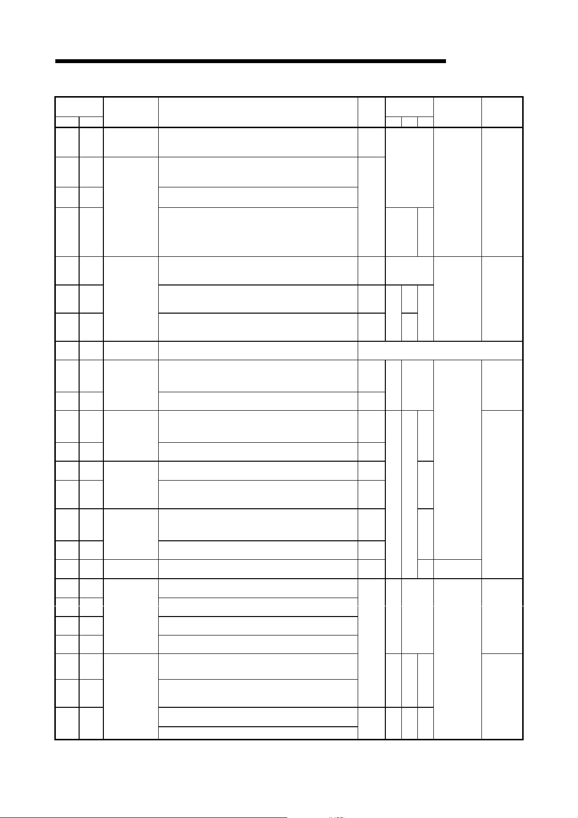
3 SPECIFICATIONS
MELSEC-Q
Address
Decimal (Hex)
CH1 CH2
312
152
)
(138H)
(98
H
153
313
(99
)
(139H)
H
154
314
(9A
)
(13AH)
H
155
315
(9B
)
(13BH)
H
156
316
(9C
)
(13CH)
H
317
157
)
(13DH)
(9D
H
158
318
(9E
)
(13EH)
H
319
159
)
(13FH)
(9F
H
160
320
(A0
)
(140H)
H
321
161
)
(141H)
(A1H
322
162
)
(142H)
(A2H
323
163
)
(143H)
(A3
H
164
324
(A4
)
(144H)
H
165
325
(A5
)
(145H)
H
326
166
)
(146H)
(A6
H
327
167
)
(147H)
(A7H
328
168
)
(148H)
(A8H
329
169
)
(149H)
(A9H
330
170
)
(14AH)
(AAH
171
331
(AB
)
(14BH)
H
172
332
(AC
)
(14CH)
H
333
173
)
(14DH)
(ADH
174 to
334 to
177
337
(AEH to
(14EH to
B1H)
151H)
178 to
338 to
181
341
(B2H to
(152H to
B5H)
155H)
Application Name
For designation
of communication control
Communication system designation (for RS-232)
0: Full duplex communication 1: Half-duplex communication
Simultaneous transmission priority/non-priority designation
0: Priority
For half- duplex
communica-tions
control
designation (RS-
232)
Other than 0: Non-priority (transmission wait time, unit: 100 ms)
Retransmission time transmission method designation
0: Do not resend . 1: Resend.
Simultaneously transmission data valid/invalid designation
• Receive data valid/invalid (b0)
0: Valid 1: Invalid
• Transmissio n da ta va l id/ in va l id (b8)
0: Valid 1: Invalid
No-reception monitoring time (timer 0) designation
: Wait infinitely
0
H
28
to FA0H: Monitoring time (unit: byte)
For designation
of data
communica-tion
time monitoring
H
Response monitoring time ( timer 1) designation
: Wait infinitely
H
0
1
to BB8H: Monitoring time (unit: 100 ms)
H
Transmission monitoring time (timer 2) designation
0
: Wait infinitely
H
1
to BB8H: Monitoring time (unit: 100 ms)
H
Use prohibited System area
For designation
of on-demand
function
Buffer memory head add re ss des ign at io n
(400H to 1AFFH, 2600H to 3FFFH)
Data length designation
(0000H to 3400H)
For designation
of transmission
area
Transmission buffe r me mory head address designation
(400H to 1AFFH, 2600H to 3FFFH)
Transmission buffer memory length designation
(0001H to 1A00H)
Received da ta count designation
0001
to 33FEH: Received data cou n t
For data
reception
H
Receive complete code designation
: No designation for re ce i ve compl et e c ode
FFFF
H
0
to FFH: Receive c o mp le te co de
H
Receive buffe r me mory head add re s s de sign at io n
For designation
of reception area
(400H to 1AFFH, 2600H to 3FFFH)
Receive buffe r me mory le ng th des igna t i on
(0001H to 1A00H)
For data
reception
Receive data c lea r re ques t
0: No request 1: Requested
First frame No. designation 1st
0: No designati on Other than 0: Des ign ated
For designation
of on-demand
user frame
First frame No. designation 2nd
0: No designati on Other than 0: Des ign ated
Last frame No. designation 1st
0: No designati on Other than 0: Des ign ated
Last frame No. designation 2nd
0: No designati on Other than 0: Des ign ated
User frame use enable/disable designation
0: Do not use 1: Use
2: Data communication possible (Q series C24 set)
For designation
of receive user
frame
First frame No. designation 1st (1st to 4th)
0H: No designation 1H or more: Head frame No.
Last frame No. designation (1st to 4th)
0H: No designation 1H or more: Last frame No.
0: No transmission designation 1 or more: Output frame No.
Initial
value
0
0
0
H
H
32
(5 sec.)
708
H
(3 min.)
CH1:
400
H
CH2:
H
800
0
CH1:
H
400
CH2:
800
H
200
H
H
1FF
0D0A
(CR+LF)
CH1:
600
H
CH2:
H
A00
200H
0
0
1: 0D
2: 0A
3: 0
H
4: 0
H
Applicable
protocol
MC Non Bi
—RW
RW
RW —
:
H
—RW
RW —
—RW—
H
H
—RW—
RW
RW
—
RW
RW
RW
—
RW
— Not allowed
Registration
allowed/not
allowed
Allowed
Allowed
—
Allowed
Allowed
Reference
section
Chapter 7
Section
8.4.5
Section
8.4.8
Chapter 8
of User's
Manual
(Application)
Section
8.4.5
Chapter 6
of User's
Manual
(Application)
Section
8.4.6
Reference
Manual
Chapter 6
Chapter 7
Section
8.4.5
Section
8.4.7
Section 8.7
Section
8.4.6
Chapters 9
and 10 of
User's
Manual
(Application)
Section
8.4.7
Chapters 9
and 11 of
User's
Manual
(Application)
3 - 21 3 - 21
Page 72

3 SPECIFICATIONS
MELSEC-Q
Address
Decimal (Hex)
CH1 CH2
342
182
)
(156H)
(B6H
183
343
(B7
)
(157H)
H
344
184
)
(158H)
(B8
H
345
185
)
(159H)
(B9H
186 to
346 to
285
445
(BAH to
(15AH to
11DH)
1BDH)
286
446
(11E
)
(1BEH)
H
287
447
(1BF
(11F
)
H
448
288
(1C0
)
(120
H
289
449
(121
)
(1C1H)
H
290 to
450 to
303
12FH)
511
(1C2H to
1EFH)
(122H to
512
(200
)
H
513
(201
)
H
514
)
(202
H
Application Name
User frame being
transmitted
User frame being transmitted
0 : Not send
1 to 100: User frame being transmitted (nth)
CR/LF output designation
0: Do not send. 1: Send.
Output head pointer designation
For user frame
being transmitted
designation
For designation
of transmission
wait time
0: No designation 1 to 100: Send from nth
Output count designation
0: No designati on 1 to 100: Output n
Output frame No. designation (A maximum of 100 can be specified)
Message wait time designation
0: No wait time 1
Transmission transparent code d esignation 1st
: No designation
0000
)
H
For designation
of transparent
code
)
H
H
Other than 0000
• Transparent code (b0 to b7)
00
H
• Additional code (b8 to b15)
H
00
Receive tr ansparent code designation
: No designation
0000
H
Other than 0000
• Transparent code (b0 to b7)
H
00
: Designated (be low)
H
to FFH: Transparent code
to FFH: Additional code
: Designated (be low)
H
to FFH: Transparent code
• Additional code (b8 to b15)
00
to FFH: Additional code
H
For conversion
designation
ASCII-BIN co nver s ion des igna t io n
0: No conversion 1: Convert
Use prohibited System area
For confirmation
of station No.
Station No. (switch setting)
setting status
LED ON status and co mmu ni ca t ion er ror st at us on C H1 si de
0: Turned off/OFF, no error 1: Turned on/ON, error
SD WAIT (b0)
SIO (b1)
PRO. (b2)
For confirmation
of LED ON status
and
communication
error status
P/S (b3)
For system (b8) to (b15)
LED ON status and co mmu ni ca t ion er ror st at us on C H2 si de
0: Turned off/OFF, no error 1: Turned on/ON, error
SD WAIT (b0)
SIO (b1)
PRO. (b2)
P/S (b3)
C/N (b4)
For system (b8) to (b13)
to FH: Wait time (unit: 10 ms)
H
C/N (b4)
NAK (b5)
ACK. (b6)
NEU. (b7)
NAK (b5)
ACK. (b6)
NEU. (b7)
CH2.ERR. (b14)
CH1 ERR. (b15)
Initial
value
Applicable
protocol
MC Non Bi
Registration
allowed/not
0 R Not allowed
—
0
—
RW
RW —
0
—RW
—
Depends
on
parame-
ter setting
Depends
on
module
status
R Not allowed
allowed
Allowed
Allowed
Reference
section
Section
8.4.7
Chapters 9
and 11 of
User's
Manual
(Application)
Section
8.4.6
Section
8.4.5
Chapter 12
of User's
Manual
(Application)
Section 4.3
Section
4.5.2
Section
8.6.9
3 - 22 3 - 22
Page 73

3 SPECIFICATIONS
MELSEC-Q
Address
Decimal (Hex)
CH1 CH2
515
)
(203
H
516
)
(204
H
517 to 541
to 21DH)
(205
H
542
)
(51E
H
543
(51F
)
H
544
(220
)
H
545
)
(221
H
546
)
(222
H
547
)
(223
H
548 to 549
to 225H)
(224
H
550
)
(226
H
Application Name
Switch setting error and mode switching error status
0: No error
Other than 0: Switch setting error and mode switching error
CH1 Communicat ion prot oc o l set t ing No. (b0 )
CH1 Communication rate setting (b1)
For confirmation
of switch setting
and mode
switching
CH1 Setting change prohibit time mode switching (b3)
CH2 Communicat ion prot oc o l set t ing No. (b4 )
CH2 Communication rate setting (b5)
CH2 Setting change prohibit time mode switching (b7)
Setting stat io n No. (b14 )
Linked operation setting (b15)
Number of registered user frames
0
: No registration 1 or more: Number of registered frames
H
User frame registration status (for confirmation of registration No.)
0: No registration 1: Registered
Bit corresponding to registration No. is 0(ON)/1(OFF).
For confirmation
Registration No.3E8
Registration No. 4AF
(1000) : Address 20 5H (b0) to
H
(1199) : Ad dress 211H (b7)
H
of user frame
Number of registered default registration frames (for system)
Use prohibited System area
For confirmation
of flash ROM
write result
Flash ROM system parameters write result
0 : Normal completion
Other than 1 (erro r code ) : A bnor mal co mple t ion
Modem function err or cod e (e rro r co de w hen mode m fun ct ion is
being used)
0 : Normal completion
Other than 1 (erro r code ) : A bnor mal co mple t ion
Modem function sequence status
0: Idle
1: Waitin g for initializ a t ion
2: Initializing modem
3: Waiting
For confirmation
of modem
function
4: Checking password
5: Communicating
6: Notification in progress
Number of data registration for connection
0: No registration 1 or more: Number of registration
Data registration status for connection
(for confirmation of registration No.)
0: No registration 1: Registered
Bit corresponding to registration No. is 0(ON)/1(OFF).
Registration No. BB8
Registration No. BD5
(3000) : Address 224H (b0) to
H
(3029) : Address 2 25H (b13)
H
Number of data registration for initialization
0: No registration 1 or more: Number of registrations
0: Normal 1: Error
0: Normal 1: Error
0: Normal 1: Error
0: Normal 1: Error
0: Normal 1: Error
0: Normal 1: Disable
0: Normal 1: Out of range
0: Normal 1: Error
7: Modem disconnected
8: Callback Request reception waiting
9: Callbac k Modem disconnect waiting
10: Callb ac k Delay time waiting
11: Callback Reconnecting
12: Callba ck Re checking password
Initial
value
Applicable
protocol
MC Non Bi
0R
Depends
on
registration
status
R — Not allowed
RW Not allowed
0
R Not allowed
Registration
allowed/not
allowed
Not allowed
—
Reference
section
Section 4.3
Section
4.5.2
Section
8.6.9
Section
8.6.9
Section
8.6.9
Section
9.1.2 of
User's
Manual
(Application)
Section
8.6.9
Section
8.6.2
Chapter 3
of User's
Manual
(Application)
3 - 23 3 - 23
Page 74

3 SPECIFICATIONS
MELSEC-Q
Address
Decimal (Hex)
CH1 CH2
551 to 552
(227
to 228H)
H
553
)
(229
H
554
)
H
(22A
555 to 557
to 22DH)
(22B
H
558 to 561
(22E
to 231H)
H
562 to 565
(232
to 235H)
H
566 to 569
(236
to 239H)
H
570 to 573
(23A
to 23DH)
H
574 to 590
(23E
to 24EH)
H
591
(24F
)
H
592
608
(250
)
(260H)
H
593
609
(251
)
(261H)
H
594
610
(252
)
(262H)
H
595
611
(253
)
(263H)
H
596
612
(254
)
(264H)
H
Application Name
Data registration status for initialization
For confirmation
of modem
function
(for confirmation of registration No.)
0: No registration 1: Registered
Bit corresponding to registration No. is 0(ON)/1(OFF).
Registration No.9C4
Registration No. 9E1
(2500) : Address 227H (b0) to
H
(2529) : Address 228H (b13)
H
Number of notification execution
0: Not executed 1 or more: Number of executions
Notificat ion exec ut io n da ta No.
0 : Notification not executed
BB8
or more: Notification executed
H
(notification execution No.)
System area (use proh i b ited) —
For confirmation
of notification
status
Data
storage
area 1
Data storage area 2
Data storage area 3
The configuration of each area is the same as the data storage area 1.
Data storage area 4
Data storage area 5
Use prohibited System area
For confirmation
of station No.
setting status
(
3)
Station No. (instruction setting)
Communication protocol status (switch setting)
0: GX Developer connection
1: MC protocol (format 1)
2: MC protocol (format 2)
3: MC protocol (format 3)
4: MC protocol (format 4)
Transmission setting status (switch setting)
Operation setting (b0)
Data bit (b1)
Parity bit (b2)
Odd/even parity (b3)
Stop bit (b4)
Sum check code (b5)
Write during RUN (b6)
Setting modification (b7)
For confirmation
of transmission
control status
Communication rate (b8 to b11)
For system (b12 to b15)
Communication protocol status (current)
0: GX Developer connection
1: MC protocol (format 1)
2: MC protocol (format 2)
3: MC protocol (format 3)
4: MC protocol (format 4)
Transmission status (current)
Operation setting (b0)
Data bit (b1)
Parity bit (b2)
Odd/even parity (b3)
Stop bit (b4)
Sum check code (b5)
Write during RUN (b6)
Setting modification (b7)
Communication rate (b8 to b11)
For system (b12 to b15)
RS-232 control signal status
Control signal
status
0: OFF status 1: ON status
RS (b0)
DSR (b1)
DTR (b2)
CD (b3)
Not used (b6 to b15) A ll 0
5: MC protocol (format 5)
6: Non procedure protocol
7: Bidirection al pr ot ocol
8: (For linked operation)
0: Independent
0: 7 bit
0: No
0: Odd
0: 1 bit
0: No
0: Prohibited
0: Prohibited
1: Link
1: 8 bit
1: Yes
1: Even
1: 2 bit
1: Yes
1: Allowed
1: Allowed
50 bps to 230400 bp s
All 0
5: MC protocol (format 5)
6: Non procedure protocol
7: Bidirection al pr ot ocol
8: (For linked operation)
0: Independent
0: 7 bit
0: No
0: Odd
0: 1 bit
0: No
0: Prohibited
0: Prohibited
1: link
1: 8 bit
1: Yes
1: Even
1: 2 bit
1: Yes
1: Allowed
1: Allowed
50 bps to 230400 bp s
All 0
CS (b4)
RI (b5)
Initial
value
Applicable
protocol
MC Non Bi
0R
0R
Depends
on module
status
Depends
on
parameter
setting
Depends
on signal
status
R
R
R
Registration
allowed/not
allowed
Not allowed
—
Not allowed
Not allowed
Reference
section
Section
8.6.2
Chapter 3
of User's
Manual
(Application)
Section
4.5.2
Section
8.6.3
Section
10.1.6
Section
4.5.2
Section
8.6.3
Section
10.1.5
Section
4.5.2
Section
8.6.3
Section
10.1.6
Section
8.6.3
Section
10.1.3
3 - 24 3 - 24
Page 75

3 SPECIFICATIONS
MELSEC-Q
Address
Decimal (Hex)
CH1 CH2
597
613
(255
)
(265H)
H
598
614
(256
)
(266H)
H
599
615
(257
)
(267H)
H
600
616
(258
)
(268H)
H
601
617
(259
)
(269H)
H
618
602
)
(26AH)
(25A
H
603
619
(25B
)
(26BH)
H
604 to
620 to
607
1023
(25C
(26CH to
H
to 25FH)
3FFH)
2048
1024
)
(800H)
(400
H
1025 to
2049 to
1535
2559
(401H to
(801H to
5FFH)
9FFH)
2560
1536
)
(A00H)
(600
H
1537 to
2561 to
2047
3071
(601H to
(A01H to
7FFH)
BFFH)
3072 to 6911
(C00H to 1AFFH)
6912to 6952
(1B00H to 1B28H)
6953 to 6993
(1B29H to 1B51H)
6994 to 7034
(1B52H to 1B7AH)
7035 to 7075
(1B7BH to 1BA3H)
7076 to 7116
(1BA4H to 1BCCH)
7117 to 7157
(1BCDH to 1BF5H)
7158 to 7198
(1BF6H to 1C1EH)
7199 to 7239
(1C1FH to 1C47H)
7240 to 7280
(1C48H to 1C70H)
7281 to 7321
(1C71H to 1C99H)
7322 to 7362
(1C9AH to 1CC2H)
7363 to 7403
(1CC3H to 1CEBH)
7404 to 7444
(1CECH to 1D14H)
7445 to 7485
(1D15H to 1D3DH)
Application Name
Transmission sequence status (For confirmation of MC protocol
communication status)
0: Waiting for receiving command
1: Receiving command
2: Command reception complete
3: Waiting to access PLC CPU
4: Accessing PLC CPU
5: PLC CP U ac ce s s co m p le te
6: Response message transmission
On-demand execution result
0 : Normal completion
1 or more: Abnormal completion (error code)
For confirmation
of communication result
Data transmission result
0 : Normal completion
1 or more: Abnormal completion (error code)
Data reception result
0 : Normal completion
1 or more: Abnormal completion (error code)
System area
MC protoco l transmission erro r code
(excludes A compatible 1C frame communication)
0: No error 1 or more: Transmission error code
Receive user frame (nth)
0 : Not received
1 to 4: Combination of user frame No. designations for reception
message
Use prohibited System area
Transmission dat a co un t des ign at ion
0: No designati on 1 or more: Number of send data
Transmission data designation
Transmission/rece
ive area
Data to be sent to an external device
Receive data count (Number of data for which read is requested)
0: No receive data 1 or more: Number of receive data
Receive data
Data received from an external device
For user
User free area (3 840 word s)
Determined by the user.
For registration No. 8001
For registration No. 8002
For registration No. 8003
For registration No. 8004
For registration No. 8005
For registration No. 8006
For registration No. 8007
For registration No. 8008
For registration No. 8009
For registration No. 800A
For registration No. 800B
For registration N o. 800 C
For registration N o. 800 D
For registration No. 800E
H
H
H
H
H
H
H
H
H
H
H
H
H
H
Initial
value
Applicable
protocol
MC Non Bi
R—
0
RW —
RW
RW —
0
—R—
0 RW Not allowed
0 RW Not allowed
The user registration area has the following combined uses, with
data written by the use r ac co rd in g to the pur po se of us e by the
TO instruction, etc.
See each explanation item concerning the configuration of each
area, the data written, etc.
(1) If data communications is being carri ed out by user
registration frame.
• User registration frame (User’s Manual (Application),
Chapter 9)
(2) If data communications is being carri ed out by the modem
function.
• Initialization Data (U ser’s Manual (Application) Section
3.4.3)
• Connection Data (User’s Manual (Application) Section
3.4.4)
Registration
allowed/not
allowed
Not allowed
—
Not allowed
—
Not allowed
Reference
section
Section
8.6.4
Section
10.1.4
Chapter 6
Chapter 7
Section
8.6.5
Section
8.6.6
Section
8.6.4
Section
8.6.5
Chapter 6
Chapter 7
Section
8.4.5
Section
8.4.7
—
Refer to left
description
3 - 25 3 - 25
Page 76

3 SPECIFICATIONS
MELSEC-Q
Address
Decimal (Hex)
CH1 CH2
7486 to 7526
(1D3EH to 1D66H)
7527 to 7567
(1D67H to 1D8FH)
7568 to 7608
(1D90H to 1DB8H)
7609 to 7649
(1DB9H to 1DE1H)
7650 to 7690
(1DE2H to 1E0AH)
7691 to 7731
(1E0BH to 1E33H)
7732 to 7772
(1E34H to 1E5CH)
7773 to 7813
(1E5DH to 1E85H)
7814 to 7854
(1E86H to 1EAEH)
7855 to 7895
(1EAFH to 1DE7H)
7896 to 7936
(1ED8H to 1F00H)
7937 to 7977
(1F01H to 1F29H)
7978 to 8018
(1F2AH to 1F52H)
8019 to 8059
(1F53H to 1F7BH)
8060 to 8100
(1F7CH to 1FA4H)
8101 to 8141
(1FA5H to 1FCDH)
8142 to 8182
(1FCEH to 1FF6H)
8183 to 8191
(1FF7
to 1FFFH)
H
8192
(2000
)
H
8193
(2001
)
H
8194
(2002
)
H
8195 to 8198
H to 2006H)
(2003
8199
(2007
)
H
8200
(2008
)
H
8201
(2009
)
H
8202
)
H
(200A
8203
(200B
)
H
8204
(200C
)
H
8205
)
H
(200D
Application Name
For registr ation No. 800F
For registration No. 8010
For registration No. 8011
For registration No. 8012
For registration No. 8013
For registration No. 8014
For registration No. 8015
For registration No. 8016
For registration No. 8017
For registration No. 8018
For registration No. 8019
For registration No. 801A
For registration No. 801B
For registration N o. 801 C
For registration N o. 801 D
For registration No. 801E
For registr ation No. 801F
H
H
H
H
H
H
H
H
H
H
H
H
H
H
H
H
H
Use prohibited System area
System
designation
Flash ROM write allow/prohibit designation
0: Write prohibited 1: Write allowed
Callback function designation
: Auto
H
0
: Callback connection (during fixed)·····························(Setting 4)
1
H
: Callback connect ion (d ur in g de sign a ted nu mber) ··· · ·( Sett ing 5)
H
3
: Callback connect io n
H
7
(during max. designated number is 10)·····················(Setting 6)
: Auto/Callback connection (during fixed)·····················(Setting 1)
H
For callback
function
9
: Auto/Callback connection
H
B
(during designated number)·······································(Setting 2)
: Auto/Callba ck co nn ec t io n
H
F
(during max. designated number is 10)·····················(Setting 3)
Callback den ia l not if ica t io n ac cu mu late d co un t de s ign at ion
H
: Not specif i ed
0
H
to FFFFH: Notification accumulated number count
1
Use prohibited System area
Auto modem init ial iza t ion d esi gna tio n
0: Do not auto initialize 1: Auto initialize
Modem initialization time DR (DSR) signal valid/invalid designation
For designation
of modem
function -2
0: Do not ignore DR sign al . 1: Ignore DR sign al.
Complete signal handling for modem function designation
0: Do not turn on/off X13 to X16.
1: Turn on/off X13 to X16.
Wait time of notification designation
to FFFFH: Wait time (unit: s)
0000
H
Use prohibited System area
Remote password mismatch notification count designation
0
: No designation
H
to FFFFH: Notification times
H
For remote
password
function
1
Remote password mi s mat ch not ifi c at ion ac c u mula te d coun t
designation
0
: No designation
H
1
to FFFFH: Cumulative times of notification
H
Initial
value
Applicable
protocol
MC Non Bi
The user registration area has the following combined uses, with
data written by the use r ac co rd in g to the pur po se of us e by the
TO instruction, etc.
See each explanation item concerning the configuration of each
area, the data written, etc.
(1) If data communications is being carri ed out by user
registration frame.
• User registration frame (User’s Manual (Application),
Chapter 9)
(2) If data communications is being carri ed out by the modem
function.
• Initialization Data (U ser’s Manual (Application) Section
3.4.3)
• Connection Data (User’s Manual (Application) Section
3.4.4)
0 RW Not allowed
0
— Allowed
RW
1
0
1
RW Allowed
1
10
0
—
RW
1
Registration
allowed/not
allowed
Not allowed
—
—
—
Allowed
Reference
section
Refer to left
description
Section
8.4.12
Section
8.4.4
Chapter 3 of
User’s
Manual
(Application)
Section
8.4.4
Chapter 3
of User's
Manual
(Application)
Section 5.1.5
Section 8.4.4
Chapter 3 of
User's
Manual
(Application)
3 - 26 3 - 26
Page 77

3 SPECIFICATIONS
MELSEC-Q
Address
Decimal (Hex)
CH1 CH2
8206
(200E
H
8456 to
8463
8207
(2108H
(200FH)
210FH)
8208
8464
(2010H)
(2110H)
8209
8465
(2011H)
(2111H)
8210
8466
(2012H)
(2112H)
8211
8467
(2013H)
(2113H)
8212
8468
(2014H)
(2114H)
8213 to
8469 to
8215
8471
(2015H
(2115H
to
2017H)
2117H)
8216
8472
(2018H)
(2118H)
8217
8473
(2019H)
(2119H)
8218
8474
(201AH)
(211AH)
8219
8475
(201BH)
(211BH)
8220 to
8476 to
8223
8479
(201CH
(211CH
to
201FH)
211FH)
8224 to
8480 to
8227
8483
(2020
(2120
H
to
2023H)
2123H)
8228 to
8484 to
8231
8487
(2024H
(2124H
to
2027H)
2127H)
8232 to
8488 to
8239
8495
(2028H
(2128H
to
202FH)
212FH)
8240 to
8496 to
8248
8504
(2030
(2130
H
to
2038H)
2138H)
8249 to
8505 to
8255
8511
(2039
(2139
H
to
203FH)
213FH)
Application Name
For designation
of modem
)
function -3
Use prohibited System area
to
Interrupt
designation
Circuit disconnect wait time (PLC CPU watch use)
0000
to FFFFH: Wait time (unit: s)
H
Receive interrupt-issued designation
0: Do not issue interrupt. 1: Issue interrupt.
Initial
value
Applicable
protocol
MC Non Bi
0
RW
0 — RW Allowed
Use prohibited System area
For transm ission
control
designation (
Transmission con tr o l star t f ree area de si gn atio n
64 to 4,095: transmission control start free area
Transmission contr o l end free ar ea des ig nat ion
263 to 4096: transmission control end free area
Non procedure and non reception monitoring time format
1)
designation
64
263
RW
—
RW
0
0: Format-0 1: Format-1
Use prohibited System area
to
Communication data monitoring designation
0000
: No monitor/stop ped moni tor des ign at io n
H
: Monitor start designation
H
0001
: Monitoring (Q series C24 is a set.)
0002
H
1002
: Monitoring stopped (Q series C24 is set.)
H
: Monitor setting erro r (Q seri es C24 i s a set .)
100F
H
0
Data optional designation
Communication
data monitoring
function (
1)
0: Off 1: On
Full stop designation (b0)
Timer 0 errors at occurrence stop designation (b2)
For system (b1) , (b3) to (b1 5)
0
RW Allowed
CH1:
2600
CH2:
3300
0D00
H
H
H
Use prohibited System area
to
Monitor buffer head address designation
to 1AFDH,2600H to 3FFDH)
H
(400
Monitor buffer size designation
to 1A00H)
H
(0003
User frame receive format designation (1st to 4th)
H
to
For designation
of user frame
receiving method
to
Use prohibited System area —
to
0: Format-0, 1: Format-1
Exclusive format-1 received data count (1st to 4th)
0 or more: Exclusive format-1 received data count
0
—
RW
Transmission transparent code d esignation (2nd to 4th)
For designation
H
of transparent
to
code
0000
H
Other than 0000
• Transparent code (b0 to b7)
00
to FF
H
H
:No designation
H
:Designated (b e low)
: Transparent code
0
—
• Additional code (b8 to b15)
H
Use prohibite d
to
to FF
H
00
System area
H
: Addition al co de
Registration
allowed/not
allowed
—
Allowed
—
—
Allowed
—
—
—
Allowed
—
RW Allowed
—
Reference
section
Section 8.4.4
Chapter 3 of
User's
Manual
(Application)
Chapter 4 of
User's Manual
(Application)
Chapter 7 of
User’s
Manual
(Application)
Chapter 6 of
User’s
Manual
(Application)
Chapter 16
of User’s
Manual
(Application)
Section
3.4.7
Chapter 11
of User's
Manual
(Application)
Section
3.4.5
Chapter 12
of User's
Manual
(Application)
3 - 27 3 - 27
Page 78

3 SPECIFICATIONS
MELSEC-Q
Address
Decimal (Hex)
CH1 CH2
8256
8512
(2040H)
(2140H)
8257
8513
(2041H)
(2141H)
8258
8514
(2042H)
(2142H)
8259
8515
(2043H)
(2143H)
8260
8516
(2044H)
(2144H)
8261
8517
(2045H)
(2145H)
8262
8518
(2046H)
(2146H)
8263 to
8519 to
8268
8524
(2047H to
(2147H to
204CH)
2149H)
8269
8225
(204DH)
(214DH)
8270
8226
(204EH)
(214EH)
8271
8527
(204FH)
(214FH)
8272
8528
(2050H)
(2150H)
8273 to
8529 to
8274
8530
(2051H to
(2151H to
2052H)
2152H)
8275
8531
(2053H)
(2153H)
8276
8532
(2054H)
(2154H)
8277
8533
(2055H)
(2155H)
8278
8534
(2056H)
(2156H)
8279
8535
(2057H)
(2157H)
8280
8536
(2058H)
(2158H)
8281 to
8537 to
8361
8617
(2059H to
(2159H to
20A9H)
21A9H)
8362 to
8618 to
8421
8677
(20AAH to
(21AAH to
20E5H)
21E5H)
Application
Cycle time unit s de s ign ati on
0: 100 ms 1: s 2: min
Cycle time designation
0H : No designation
to FFFFH: PLC CPU monitoring cycle time
H
1
PLC CPU monitor in g fu nct io n de sign at i o n
0: Do not use the f un ctio n. 1: Fixed cycle transmissi on
2: Condition agreement transmi ssion
PLC CPU monitoring transmission measure designation
For designation
of PLC CPU
monitoring
function
(for fixed cycle transmission)
0: Data trans miss ion (dev i ce da ta an d C PU st at u s data)
1: Notification
Transmission pointer designation (For fixed cycle transmission and
data transmi ssi on)
1 to 100: Output head poi nt ( send fro m t he nt h)
Send the user fra mes de si gnat ed in th e f ollow ing tra nsmis s ion
frame No. design ation are as fr o m the desi gn ate d p oin ter po sit ion .
(addresses: CH1 side = BA
Output count designation (for fixed cycle transmission and data
transmission)
1 to 100:Output count (designate the nu mber of fra me transmissions.)
Data No. for co nne ct ion des igna t io n (f or fixe d cycle transmission
and notification)
0BB8
to 0BD5H, 8001H to 801FH: Data No. for connection
H
Use prohibite d
System area
Number of registered word blocks designation
0 : No designation
1 to 10: Number of blocks of word devices
Number of registered bit blocks designation
0 : No designation
1 to 10: Number of blocks of bit devices
PLC CPU abnormal monitoring designation
0: Do not monitor. 1: Monitor.
For designation
of PLC CPU
monitoring
function
No. 1
block
monitoring
device
For designation
of PLC CPU
monitoring
function
Block
monitoring
devices
No. 2 to
10
Use prohibited System area
Name
Initial
value
Applicable
protocol
MC Non Bi
2
H
5
0
R — Allowed
0
to 11DH, CH2 side = 15 AH to 1BDH)
H
It is possible to
designate a
maximum of 10
blocks in total.
Monitoring device designation
90H to CCH: Device code
Head device No. designation
0 or more: Head device No.
Read point designation
1 or more: Number to read points
Monitoring condition designation (judgment condition
designation)
1 or more: Monitoring condition
Monitoring condition value designation
0R—
At bit device 0: OFF 1: ON
: Monitoring condition value
At word device 0 to FFFF
Transmission pointer designation (for condition
agreement transmission and data transmission)
1 to 100: Output head point (send from nth)
Send the user frames designated in the following
transmission frame No. designation areas from the
designated pointer position.
(address: CH1 side = BAH to 11DH, CH2 side = 15AH
to 1BDH)
H
Output count designation (for condition agreement
transmission and data transmission)
1 to 100: Output coun t (de sign at e th e nu mber
of frame transmissions)
Data No. for connection designation (for condition
agreement transmission and notification)
to 0BD5H, 8001H to 801FH: Data No. for
H
0BB8
connection
The structure of each area is the same as the first block monitoring device area
See *2 for the deta i ls of eac h ar ea .
Registration
allowed/not
allowed
—
Allowed
—
Reference
section
Chapter 2
of User's
Manual
(Application)
Chapter 2
of User's
Manual
(Application)
3 - 28 3 - 28
Page 79

3 SPECIFICATIONS
MELSEC-Q
Address
Decimal (Hex)
CH1 CH2
8422
8678
(20E6H)
(21E6H)
8423
8679
(20E7H)
(21E7H)
8424
8680
(20E8H)
(21E8H)
8425 to
8681 to
8447
8703
(20E9H to
(21E9H to
20FFH)
21FFH)
8448 (2100H)
8449 (2101H)
8450 (2102H)
8451 (2103H)
8452 (2104H)
8453 (2105H)
8454 (2106H)
8455 (2107H)
8456 (2108H)
8457 (2109H)
8458 (210AH)
8704 to
8960 to
8707
8963
(2200H to
(2300H to
2203H)
2303H)
8708
8964
(2204H)
(2304H)
8709
8965
(2205H)
(2305H)
8710
8966
(2206H)
(2306H)
8711
8967
(2207H)
(2307H)
8712 to
8968 to
8954
9215
(2208H to
(2308H to
22FAH)
23FFH)
Application Name
Transmission pointer designation (for condition
agreement transmission)
1 to 100: Output head point (send from nth)
Send the user fra me s des ign ated in the fo llow ing
transmission frame No. designation areas from the
designated pointer position.
For designation
of PLC CPU
monitoring
function
CPU
abnormal
monitoring
designation
(address: CH1 side = BA
15A
to 1BDH)
H
Output count designation (for condition agreement
transmission)
1 to 100: Output coun t (de sign at e th e nu mber of
frame transmissions)
Data No. for co nnec t ion des igna t io n (f or cond it io n
agreement tr an smis s ion an d no t if ica t ion )
0BB8H to 0BD5H, 8001H to 801FH: Data No. for
Use prohibited System area
Use Prohibited Sys tem are a
Data No. for callback designation 1
to 0BD5H, 8001H to 801FH: Data number for callback.
0BB8
H
Data No. for callback designation 2
Data No. for callback designation 3
For callback
function
Data No. for callback designation 4
Data No. for callback designation 5
Data No. for callback designation 6
Data No. for callback designation 7
Data No. for callback designation 8
Data No. for callback designation 9
Data No. for callback designation 10
Use prohibited System area
PLC CPU monitor ing fu nc t ion ope ra t ion st atus
0: Not executed (waiting for registration of PLC CPU monitoring)
1: Wait for PLC CPU monitoring time
(waiting to access PLC CPU)
2: Accessing PLC CPU
3: Sending monitoring results
PLC CPU monitor ing fu nc t ion ex ec ut ion resu l t (curre nt )
PLC CPU
monitoring
function
0: Normal completion
1 or more: Abnormal completion (error code)
PLC CPU monitor in g fu nct io n nu mber of tran smi s sion
0: Not executed
1 or more: Number of transmissions
Monitoring condition arriva l block No.
0 : The monitoring condition is not enabled for any block
1 to 10: Registration order of word/bit block (nth)
4096 : CPU abnormal monitoring block
The latest block No. for which monitoring condition is enabled is
stored.
Use prohibited System area
to 11DH, CH2 side =
H
connection
Initial
value
Applicable
protocol
MC Non Bi
Registration
allowed/not
allowed
0 R — Allowed
—
—
0RW—
Allowed
—
0 R — Not allowed
—
Reference
section
Chapter 2
of User's
Manual
(Application)
Section
8.4.4
Chapter 3 of
User’s
Manual
(Application)
Chapter 2
of User's
Manual
(Application)
3 - 29 3 - 29
Page 80

3 SPECIFICATIONS
MELSEC-Q
Address
Decimal (Hex)
CH1 CH2
8944 (22F0H)
8945 (22F1H)
8946 (22F2H)
8947 (22F3H)
8948 (22F4H)
8949 to 8954
(22F5H to 22FAH)
8955 (22FBH)
8956(22FCH)
8957 to 8958
(22FDH to 22FEH)
8959(22FFH)
9216(2400H)
9217(2401H)
9218 to 9427
(2402H to 25FFH)
9728 to 16383
(2600H to 3FFFH)
Application Name
Callback per mi t ac cumu la te d co un t
0 or more : Accu mu la te d co un t
Callback denial accumulated count
0 or more : Accu mu la te d co un t
For callback
function
Use prohibited System area
For the remote
password
function
Use prohibited System area
For the remote
password
function
Use prohibited System area
For flash ROM
write count
housing
Use prohibited System area
For user ( 1)
Auto (callback) connection permit accumulated count
0 or more : Accu mu la te d co un t
Auto (callback) connection denial accumulated count
0 or more : Accu mu la te d co un t
Accumulated count of callback receive procedure cancel
0 or more : Accu mu la te d co un t
Accumulated coun t of un lo c k proc es s no r mal co mpl et ion
0 or more: Accumulated count of normal completion
Accumulated count of un lo ck pro c ess ab nor ma l compl et ion
processing
0 or more: Accumulated count of abnormal completion
Accumulated count of lock process based on circuit disconnection
0 or more: Accumulated count of lock process based on circuit
disconnect ion
Flash ROM write count
0 to 1000: Write co un t
User free area 2 (6 656 word s)
(Transmission/receiving data monitoring function default buffer)
Usage is determined by the user.
1 Only QJ71C24N (-R2/R4) is usable. (System area when using QJ71C24 (-R2)
2 The following tables show the areas of block monitoring devices No. 1 to 10 (CH1
side: 8272 to 8361 (2 050
which are assigned for designating the PLC CPU monitoring function.
Initial
value
MC Non Bi
0RW
Applicable
protocol
—
Registration
allowed/not
allowed
Not allowed
Reference
section
Section
8.6.2
Chapter 3 of
User's
Manual
(Application)
—
Section
5.1.5
Section
0RW
—
Not allowed
8.6.2
Chapter 3 of
User's
Manual
(Application)
—
Section
5.1.5
Section
0RW
—
Not allowed
8.6.2
Chapter 3 of
User's
Manual
(Application)
—
0 R Not allowed
—
0 RW Not allowed
H
to 20A9H), CH2 side: 8528 to 861 7 (21 50H to 21A9H)),
—
—
3 - 30 3 - 30
Page 81

3 SPECIFICATIONS
[CH1 side buffer memory address: decimal (hexadecimal)]
nth block monitoring device
12345678910
8272
(2050
8273 to
8274
(2051H to
2052H)
8275
(2053
8376
(2054
8277
(2055
8278
(2056
8279
(2057
8280
(2058
8528
(2150
8529 to
8530
(2151H to
2152H)
8531
(2153
8532
(2154
8533
(2155
8534
(2156
8535
(2157
8536
(2158
H
H
H
H
H
H
H
)
)
)
)
)
)
)
8281
(2059H)
8282 to
8283
(205AH to
205BH)
8284
(205CH)
8385
(205DH)
8286
(205EH)
8287
(205FH)
8288
(2060H)
8289
(2061H)
8290
(2062H)
8291 to
8292
(2063H to
2064H)
8293
(2065H)
8294
(2066H)
8295
(2067H)
8296
(2068H)
8297
(2069H)
8298
(206AH)
8299
(206BH)
8300 to
8301
(206CH to
206DH)
8302
(206EH)
8303
(206FH)
8304
(2070H)
8305
(2071H)
8306
(2072H)
8307
(2073H)
8308
(2074H)
8309 to
8310
(2075H to
2076H)
8311
(2077H)
8312
(2078H)
8313
(2079H)
8314
(207AH)
8315
(207BH)
8316
(207CH)
8317
(207DH)
8318 to
8319
(207EH to
207FH)
8320
(2080H)
8321
(2081H)
8322
(2082H)
8323
(2083H)
8324
(2084H)
8325
(2085H)
8326
(2086H)
8327 to
8328
(2087H to
2088H)
8329
(2089H)
8330
(208AH)
8331
(208BH)
8332
(208CH)
8333
(208DH)
8334
(208EH)
8335
(208FH)
8336 to
8337
(2090H to
2091H)
8338
(2092H)
8339
(2093H)
8340
(2094H)
8341
(2095H)
8342
(2096H)
8343
(2097H)
8344
(2098H)
8345 to
8346
(2099H to
209AH)
8347
(209BH)
8348
(209CH)
8349
(209DH)
8350
(209EH)
8351
(209FH)
8352
(20A0H)
8353
(20A1H)
8354 to
8355
(20A2H to
20A3H)
8356
(20A4H)
8357
(20A5H)
8358
(20A6H)
8359
(20A7H)
8360
(20A8H)
8361
(20A9H)
[CH2 side buffer memory address: decimal (hexadecimal)]
nth block monitoring device
12345678910
H
H
H
H
H
H
H
)
)
)
)
)
)
)
8537
(2159H)
8538 to
8539
(215AH to
215BH)
8540
(215CH)
8541
(215DH)
8542
(215EH)
8543
(215FH)
8544
(2160H)
8545
(2161H)
8546
(2162H)
8547 to
8548
(2163H to
2164H)
8549
(2165H)
8550
(2166H)
8551
(2167H)
8552
(2168H)
8553
(2169H)
8554
(216AH)
8555
(216BH)
8556 to
8557
(216CH to
216DH)
8558
(216EH)
8559
(216FH)
8560
(2170H)
8561
(2171H)
8562
(2172H)
8563
(2173H)
8564
(2174H)
8565 to
8566
(2175H to
2176H)
8567
(2177H)
8568
(2178H)
8569
(2179H)
8570
(217AH)
8571
(217BH)
8572
(217CH)
8573
(217DH)
8574 to
8575
(217EH to
217FH)
8576
(2180H)
8577
(2181H)
8578
(2182H)
8579
(2183H)
8580
(2184H)
8581
(2185H)
8582
(2186H)
8583 to
8584
(2187H to
2188H)
8585
(2189H)
8586
(218AH)
8587
(218BH)
8588
(218CH)
8589
(218DH)
8590
(218EH)
8591
(218FH)
8592 to
8593
(2190H to
2191H)
8594
(2192H)
8595
(2193H)
8596
(2194H)
8597
(2195H)
8598
(2196H)
8599
(2197H)
8600
(2198H)
8601 to
8602
(2199H to
219AH)
8603
(219BH)
8604
(219CH)
8605
(219DH)
8606
(219EH)
8607
(219FH)
8608
(21A0H)
8609
(21A1H)
8610 to
8611
(21A2H to
21A3H)
8612
(21A4H)
8613
(21A5H)
8614
(21A6H)
8615
(21A7H)
8616
(21A8H)
8617
(21A9H)
3 Only the QJ71C24N(-R2/R4) whose first 5 digits of the serial No. are 06062 or
later is applicable. (System area for other than the one described on the left)
MELSEC-Q
Name
Monitoring device designation
Head device No. designation
Designation of number of points read
Monitoring condition designation (Judgment
condition designation)
Monitoring condition value designation
Transmission pointer designation (for
conditional transmission, data transmission)
Designation of number of outputs (for
conditional transmission, data transmission)
Designation of da ta No. fo r co nne c t ion
(for condit iona l tr an s miss ion and no t if ica t ion )
3 - 31 3 - 31
Page 82
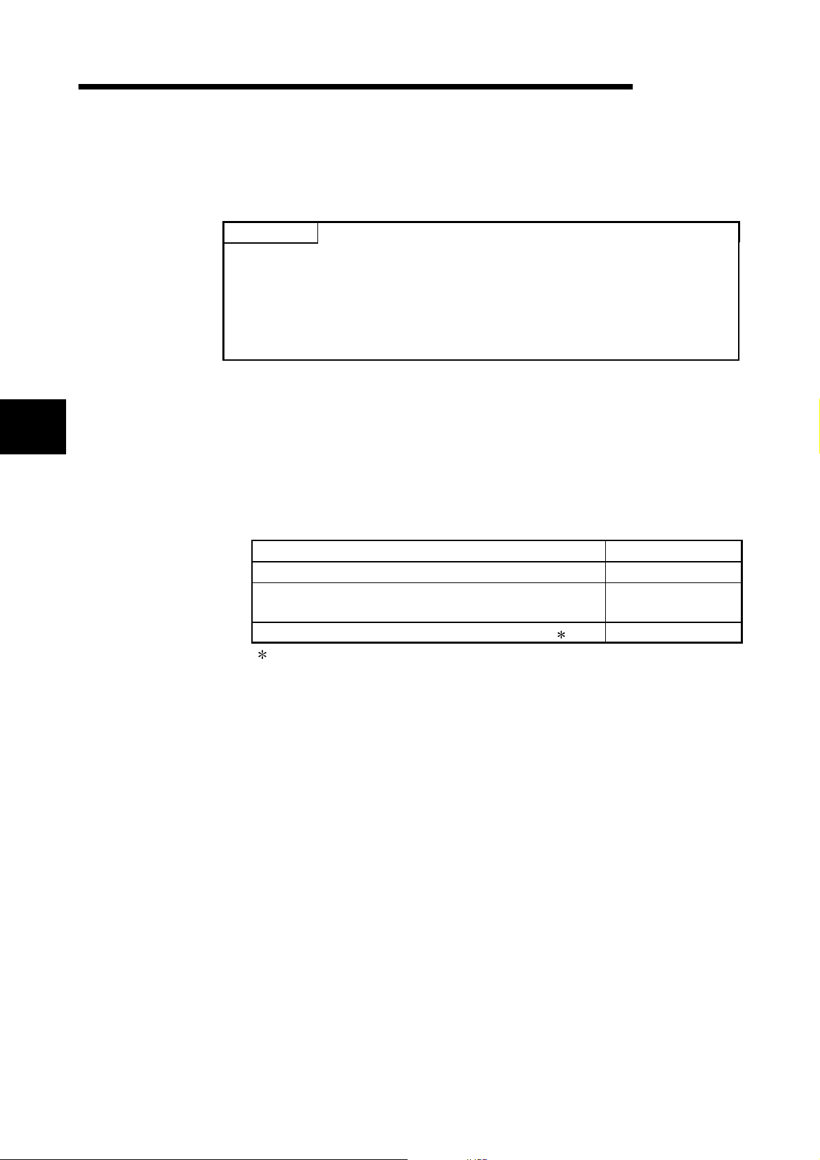
4 SETTINGS AND PROCEDURES PRIOR TO OPERATION
4 SETTINGS AND PROCEDURES PRIOR TO OPERATION
This chapter explains the settings and procedures required before starting a system
that uses the Q series C24.
POINT
(1) When using the Q series C24, please read the safety precautions at the
beginning of this manual.
(2) The installat ion an d set up met h ods o f th e Q se rie s C24 are t he sa me as th o se
for CPU modules.
(3) For module installation and setup, see the user's manual for the PLC CPU
used.
4.1 Handling Precautions
MELSEC-Q
4
The following explains the precautions for handling the Q series C24:
(1) Do not drop the module or subject it to heavy impact since it is made of resin.
(2) Tighten the module terminal and fixing screws within the specified tightening
torque range as follows:
Screw location Tightening torque range
RS-422/485 terminal block terminal screws (M3 screw ) 0.42 to 0.58 N · m
RS-422/485 plug-in connector socket terminal screw for
QJ71C24N-R4 (M2 screw)
Module fixing screw (normally not required) (M3 screw) ( 1) 0.36 to 0.48 N · m
1 A module can be easily fixed to a base unit using the hooks in the upper part
of the module. However, it is recommended that the module be fixed using
the module mounting screws when it is used in a place subject to vibration or
impact.
0.20 to 0.25 N · m
4 - 1 4 - 1
Page 83

4 SETTINGS AND PROCEDURES PRIOR TO OPERATION
C
(App
)
4.2 Settings and Procedures Prior to Operation
The outline of the procedure before operation is shown below.
Start
Check which functions and
specifications are to be used
MELSEC-Q
Connect the module with an
external device using a cable
Connect GX Developer and
QCPU with a cable
Perform various settings with
GX Developer
Perform individual station tests
with GX Developer
Perform a loopback test from the
external device
Set an operation mode with
GX Developer
• Connection of the Q series C24 and an external device
• See Section 4.4 in this manual.
• I/O assignment setting of the Q series C24
• Setting of operation mode and transmission specifications for
the Q series C24 and the external device
• See Section 4.5 in this manual.
• ROM/RAM/switch tests of the Q series C24
• Self-loopback test of the Q series C24
• See Section 4.7 in this manual
• When communication using the MC protocol is possible between
the Q series C24 and the external device, set the operation mode for
MC protocol communication and perform a loopback test.
• See Section 4.8 in this manual.
• Set an operation mode for the data communication system
between the Q series C24 and the external device.
• See Section 4.5.2 in this manual.
4
Perform auto refresh setting
with GX Configurator-SC
and error data to the GX Configurator-SC device.
• See Sections 4.6 and 8.3 in this manual.
• It is possible to change setting values for
• A setting that automatically refreshes the status of the Q series C24
Change setting values to use various
functions with GX Configurator-SC
various functions, including special functions.
• See the explanation for each function in
the applicable sections and manuals.
• See Chapter 8.
• Transmission and reception for the data communication system
Transmission and receive data
ommunication using non
procedure protocol
(see Chapter 6)
Communication using
bidirectional protocol
(see Chapter 7)
• See the explanation for each function in the applicable sections
and manuals.
Communication using MC protocol
(see the Reference Manual)
Communication using
special functions
see the U ser's
Manual
4 - 2 4 - 2
lication
Page 84

4 SETTINGS AND PROCEDURES PRIOR TO OPERATION
2
4.3 Part Names and Functions
Part names of Q series C24 are shown below.
QJ71C24N
QJ71C24 ( 2)
( 1)
QJ71C24N-R2
QJ71C24-R2
MELSEC-Q
QJ71C24N-R4
2)
2)
QJ71C24N-R2
RUN
NEU.
SD
CH1
RD
CH1
RS-232
CH2
RS-232
QJ71C24N-R2
ERR.
NEU.
SD
RD
CH2
QJ71C24N
RUN
ERR.
NEU.
CH1
CH1
RS-232
SDA
SG
SDB
(FG)
RDA
(FG)
RDB
CH2
RS-422
/485
NEU.
SD
SD
CH2
RD
RD
1
2
3
4
5
6
7
1) 1) 1)
)
3)
1 The external diagrams of the QJ71C24 are the same as QJ71C24N (except for the model name).
2 The external diagrams of the QJ71C24-R2 are the same as QJ71C24N-R2 (except for the model
name).
4)
4)
QJ71C24N-R4
RUN
NEU.
SD
CH1
RD
CH1
RS-422/485
SDA
SDB
RDA
RDB
SG
(FG)
CH2
RS-422/485
SDA
SDB
RDA
RDB
SG
(FG)
QJ71C24N-R4
ERR.
NEU.
SD
RD
CH2
Name Contents
1) Display LED Display LED (For details, see (1).)
2) RS-232 interface
3) RS-422/485 interface
4) RS-422/485 interface
RS232 interface for serial communication with external
devices (D-Sub 9 pin)
RS422/485 interface for serial communication with external
devices (2-piece terminal block)
RS422/485 interface for serial communication with external
devices (2-piece plug-in socket block)
4 - 3 4 - 3
Page 85

4 SETTINGS AND PROCEDURES PRIOR TO OPERATION
(1) LED display list
MELSEC-Q
QJ71C24N
RUN
NEU.
SD
CH1
RD
ERR.
NEU.
SD
RD
CH2
QJ71C24N-R2
RUN
NEU.
SD
CH1
RD
ERR.
NEU.
SD
RD
CH2
CH LED Display contents On/flashing Off
RUN Normal operation display Normal Faulty or reset
—
ERR Error display (
NEU
(
CH1
SD
Neutral status on the CH1
3)
side display ( 2)
Transmission status
display
1) Error has occurred Normal
Waiting for MC command
message to be received
MC command message
being received
Data being transmitted Data not transmitted
RD Reception status display Data being received Data not received
NEU
CH2
Neutral status on the CH2
(
3)
side display ( 2)
Transmission status
SD
display
RD Reception status display Data being received
Waiting for MC command
message to be received
Data being transmitted
MC command message
being received
MC command message
not transmitted
MC command message
not received
1 This LED comes on when an error occurs at Q series C24 hardware or during data communication.
2 This LED displays the data communication status via MC protocol. (see chapter 10.)
On: Waiting for the command message to be received from the external device.
Off: Processing the command message received from the external device.
3 This LED can be made valid also when "GX Developer connection" (0H) is specified in communication
protocol setting.
QJ71C24N-R4
CH1
RUN
NEU.
SD
RD
ERR.
NEU.
SD
RD
CH2
Compatible protocol
MC Non-procedural Bidirectional
Valid
Valid Invalid (Off)
Valid
Valid Invalid (Off)
Valid
4 - 4 4 - 4
Page 86

4 SETTINGS AND PROCEDURES PRIOR TO OPERATION
4.4 External Wiring
This section explains wiring between the Q series C24 and external device.
As the wiring precautions, external wiring which is resistant to the effects of external
noise is a prerequisite for reliable system operation and full use of the Q series C24
function.
(1) Ground the shield at only one point.
(2) When connecting with an external device using an RS-232 line, use a connector
shell as specified in Section 3.2.1 on the Q series C24 end.
(3) When connecting with an external device using an RS-422/485 cable, be sure to
note the following.
(a) QJ71C24N and QJ71C24
1) Use the RS-422/485 cable recommended in section 3.3.2.
2) The RS-422/485 interface terminal block uses M3 terminal screws.
Use suitable crimp-on terminals for the terminals.
(b) QJ71C24N-R4
1) Use the RS-422/485 cable recommended in section 3.3.2.
Be sure to strip the outer insulation layer by 7 mm before connecting
the cable to the plug-in socket block.
2) When connecting the braided shield wire inside the RS-422/485 cable,
use the plate terminals included with the product. The braided shield
wire can be conn e cte d wi th ou t the pla te te r min al . Fo u r plat e te rmi n al s
are included to connect the FG terminals of both stations. (see section
4.4.2.(6) .)
3) When connecting the plug-in socket block to the QJ71C24N-R4, be
sure to confirm the layout of the socket block, and then insert it into the
RS-422/485 connector on the QJ71C24N-R4.
MELSEC-Q
QJ71C24N-R4
ERR.
RUN
NEU.
NEU.
CH1
RS-422/485
SDA
SDB
RDA
RDB
SG
(FG)
CH2
RS-422/485
SDA
SDB
RDA
RDB
SG
(FG)
QJ71C24N-R4
SD
CH2
SD
RD
RD
CH1
SDA
SDB
RDA
RDB
SG
(FG)
7
mm
(0.28 in.)
Plate terminal
(included with product)
Braided shield wire
(4) Connect the external device according to its specifications.
(5) See Appendix 5 for the bend radius of the connection cable.
4 - 5 4 - 5
Page 87

4 SETTINGS AND PROCEDURES PRIOR TO OPERATION
4.4.1 Connecting the RS-232 interface (ful l -dupl ex communications)
The following shows the connection precautions and connection examples when using
the Q series C24 RS-232 interface for full-duplex communications.
(1) Connection precautions
(a) For further information about the following items, see the explanation in the
applicable section in the User's Manual (Application).
• Controlling the communication on the Q series C24 side by the external
device side using the CD signal of the RS-232 interface.
This is affe ct ed by the "RS - 232 CD te rmin al check setting" in "C Hn
transmission control and others system setting change" screen on GX
Configurator-SC.
• Performing half-du plex commun i cati on u sing spe ci ficati on s on t he e xternal
device side (an e xa mple o f su ch a conn e ction i s show n i n thi s section ) .
• Using modem functions.
(b) The connection cable FG signal and shield are connected as follows.
MELSEC-Q
Connection cable FG signal
Connection cable shield
To Connector
housing
DSR
DTR
Connection on the Q series C24 side Notes
Connect to the Q series C24 connector
housing
Connect to the external device FG terminal
or the Q series C24 connector housing
Do not short the communication cable FG
signal and the SG signal.
When the FG signal and the SG signal are
connected inside the external device, do not
connect the FG signal to the Q series C24.
(c) When normal data communication is not obtained due to external noise,
perform the wiring as follows:
1) Connect the FG terminals on the external device and the Q series C24
using the shield of the connection cable.
2) Signals other than SG should be connected with SG signals in the
twisted pai r.
(External device)
FG
RD
SD
DTR
DSR
SD
RD
Q series C24
Shield
SG
SG
POINT
When using an RS-232 to RS-422 converter to connect the external device and the
Q series C24, use a converter that is compatible with the external device and PLC
CPU system configuration (1:1).
4 - 6 4 - 6
Page 88

4 SETTINGS AND PROCEDURES PRIOR TO OPERATION
(2) Connection examples
(a) Connection example with an external device capable of turning on and off the
CD signal (No . 1 pin )
Q series C24
Signal name Signal name
CD
RD(RXD)
SD(TXD)
DTR(ER)
SG
DSR(DR)
RS(RTS)
CS(CTS)
RI(CI)
Pin No.
1
2
3
4
5
6
7
8
9
The CD terminal check setting is set according to the specification of the external
device. When wiring shown above, DTR/DSR control or DC code control may be
performed.
(b) Connection e xampl e wi th an e xte rn al devi ce not ca pable of turning on and off
the CD signal (No. 1 pin)
External device
MELSEC-Q
CD
RD(RXD)
SD(TXD)
DTR(ER)
SG
DSR(DR)
RS(RTS)
CS(CTS)
1) Connection example 1
Q series C24
Signal name
CD
RD(RXD)
SD(TXD)
DTR(ER)
SG
DSR(DR)
RS(RTS)
CS(CTS)
RI(CI)
Pin No.
1
2
3
4
5
6
7
8
9
External device
Signal name
CD
RD(RXD)
SD(TXD)
DTR(ER)
SG
DSR(DR)
RS(RTS)
CS(CTS)
When wiring shown above, DTR/DSR control or DC code control may be performed.
2) Connection example 2
Q series C24
Signal name
CD
RD(RXD)
SD(TXD)
DTR(ER)
SG
DSR(DR)
RS(RTS)
CS(CTS)
RI(CI)
Pin No.
1
2
3
4
5
6
7
8
9
External device
Signal name
CD
RD(RXD)
SD(TXD)
DTR(ER)
SG
DSR(DR)
RS(RTS)
CS(CTS)
When wiring shown above, DC code control may be performed.
POINT
If the PLC CPU and an external device cannot be communicated, try to perform data
communication as a connection test, using the wiring connection as shown in
Connection example 2.
If data can be communicated using the wiring connection shown in Connection
example 2, rewire after checking the interface specifications on the external device
side.
4 - 7 4 - 7
Page 89

4 SETTINGS AND PROCEDURES PRIOR TO OPERATION
4.4.2 Connecting the RS-422/485 interface
The following shows the connection precautions and connection examples when using
the Q series C24 RS -422 /4 85 int e rfa ce.
(1) Connection precautions
(a) When connecting the Q series C24 SG and FG signals to the external
device, connect them according to the specifications of the external device.
(b) Connect the shield of the connection cable to the FG terminal on either of
the connected devices.
If normal data communication is not obtained due to external noise even if
wiring is made as shown above, perform wiring as follows:
1) Connect between the FG of both stations with the shield of the
connection cable.
On the external device side, however, follow the instruction manual of
the external device.
Be sure to use the plate terminals included with the product when
connecting the braided shield wire to the QJ71C24N-R4.
MELSEC-Q
2) Connect the (FG) of the Q series C24 side to the FG terminal at the pow er
supply module of the station which has the Q series C24 is installed, or to
the FG terminal of the control panel on which the Q series C24 PLC is
installed.
3) Connect nnA and nnB of each signal in the connection cable as a pair.
Q series C24
SDA
SG
SDB
FG
RDA
FG
RDB
Correspondance of the RS-422/485 terminal block and signal location.
SDA
SDB
RDA
RDB
SG
(FG)
(FG)
External de vi ce
RDA
RDB
SDA
SDB
SG
FG
Shield
4 - 8 4 - 8
Page 90
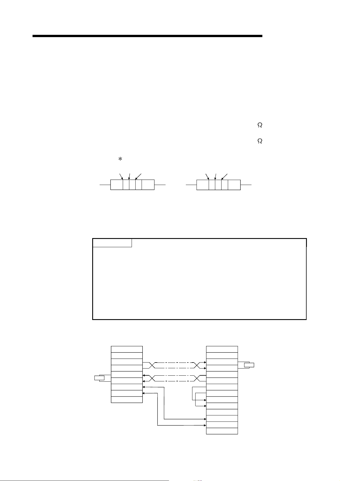
4 SETTINGS AND PROCEDURES PRIOR TO OPERATION
(c) Terminal resistor must be set (or connected) for the station of both ends on
the circuit.
Match the Q series C24 to the specifications of the external device and
connect a terminal resistor (packed with the Q series C24) according to this
section.
Connect, or set a terminal resistor at the external device according to the
instruction manual of the external device.
(The terminal resistor to connect to the Q series C24)
• When communications performed using RS-422, "330
connected.
• When communications performed using RS-485, "110
connected.
How to discriminate between the terminating resistors
330
Ω
Orange
Orange
Brown
110
Ω
Brown Brown Brown
MELSEC-Q
1/4 W" resistor is
1/2 W" resistor is
(d) If data cannot be communicated with the external device at all, the polarity of
the external device could be wrong and should be checked again. If the
polarities of the Q series C24 and the external device do not match, reverse
the polarity of each signal on either device side and connect the devices with
the cable; this may enable the data to be communicated.
POINT
(1) For terminal resistor setting/connection described in this section, when the RS-
232 to RS-422 converters or similar device is used at the external device at
both ends of the circuit, a terminal resistor must be set, or connected, at the
converter.
(2) When using the RS-232C to RS-422 converters to connect the external
devices and the Q series C24, use a converter that is compatible with the
external device and PLC CPU system configuration (1:1, 1:n, m:n).
(3) Device connected to the Q series C24 RS-422/485 interface must be
standardized as RS-422 or RS-485, including 1:n and m:n connections.
(2) Connection examples
(a) External device and Q series C24 with 1:1 system configuration
Terminal
resistor
Q series C24
Signal name
SDA
SDB
R
RDA
RDB
SG
FG
FG
External device
Signal name
RDA
RDB
SDA
SDB
RSA
RSB
CSA
CSB
Terminal
resistor
R
SG
FG
4 - 9 4 - 9
Page 91

4 SETTINGS AND PROCEDURES PRIOR TO OPERATION
(b) External device and Q series C24 with 1:n (multidrop) system configuration
1) Connection example
External device
C24 1) C24 2)
MELSEC-Q
C24n
SDA
SDB
RDA
RDB
SG
FG
R
SD
RD
RS-232
SD
RD
SDA
R
SDB
RDA
R
RDB
SG
FG
RS-422/485
cable
Linked
operation
SDA
SDB
RDA
RDB
SG
FG
RS-422/485
cable
2) Connection example 2
External device C24 1) C24 2) C24n
SDA
R
SDB
RDA
R
RDB
SG
FG
RS-422/485
cable
SDA
SDB
RDA
RDB
SG
FG
RS-422/485
cable
SDA
SDB
RDA
RDB
SG
FG
RS-422/485
cable
SDA
SDB
RDA
RDB
SG
FG
R
R
R
Terminal
resistor
R
R
Terminal
resistor
External device 1)
SDA
SDB
RDA
R
RDB
SG
FG
(c) External device and Q series C24 with n:1 (multidrop) system configuration
C24 1)
SDA
SDB
RDA
R
RDB
SG
FG
Terminal
R
resistor
RS-422/485
cable
External device 2) External device n
SDA
SDB
RDA
RDB
SG
FG
RS-422/485
cable
SDA
SDB
RDA
RDB
SG
FG
RS-422/485
cable
4 - 10 4 - 10
Page 92

4 SETTINGS AND PROCEDURES PRIOR TO OPERATION
(d) External device and Q series C24 with m:n (multidrop) system configuration
1) Connection example 1
MELSEC-Q
External device 1)
SD
RD
External device 2)
RS-232 RS-232
SD
RD
C24 1) C24 2)
SD
RD
SDA
SDB
RDA
R
RDB
SG
FG
RS-422/485
cable
Linked
operation
SD
RD
SDA
SDB
RDA
RDB
SG
FG
RS-422/485
cable
Linked
operation
C24n
SDA
SDB
RDA
R
RDB
SG
FG
Terminal
R
resistor
External device 1)
SDA
SDB
RDA
R
RDB
SG
FG
2) Connection example 2
C24 1)
SDA
SDB
RDA
RDB
SG
FG
RS-422/485
cable
RS-422/485
cable
External device 2)
SDA
SDB
RDA
RDB
SG
FG
RS-422/485
cable
C24n
SDA
SDB
RDA
R
RDB
SG
FG
Terminal
R
resistor
4 - 11 4 - 11
Page 93

4 SETTINGS AND PROCEDURES PRIOR TO OPERATION
4.5 Settings for GX Developer
This chapter explains various settings via GX Developer that allow the Q series C24 to
perform data communication with external devices.
See Section 3.3.3 of the User's Manual (Application) for how to perform the remote
password setting.
4.5.1 I/O assignment settings [Setting purpose]
The I/O assignment settings perform the settings for the types of modules to be
mounted on a base unit, the range of input/output signals, and switches of the Q
series C24.
[Startup procedure]
[GX Developer] [PLC paramet e rs] I/O assignment .
For screen display, see the GX Developer Operating Manual.
MELSEC-Q
[Setting screen]
[Display description]
Item name Setting for item Remarks
Type Select "intelli."
Model name Enter the module model name to be mounted.
(Example: QJ71C24N)
I/O
assignment
Multiple CPU settings Select when using a multiple CPU system.
Points Select 32 points.
Start XY Enter the start I/O signal (Hexadecimal) for the target module.
Switch setting Set the communication rate, transmission specifications,
communication protocol, etc.
Detailed setting Select the control PLC of the Q series C24 when a multiple
CPU system is employed.
See QCPU User's Manual
(Multiple CPU System)
See Section 4.5.2.
4 - 12 4 - 12
Page 94

4 SETTINGS AND PROCEDURES PRIOR TO OPERATION
4.5.2 Switch settings for I/O and intelligent functional module [Setting purpose]
The switch settings for I/O module and intelligent functional module perform the
settings for transmission specifications and communication protocol for
communicate with external devices.
[Setting procedure]
[GX Developer] [PLC parameters] [I/O assignment setting]
Switch setting .
For screen display, see the GX Developer Operating Manual.
[Setting screen]
MELSEC-Q
[Display description]
(1) Switches 1 to 5
Set the transmission specifications and communication protocol of each interface
using the combinations of setting values for each switch with 16 bit binary data
according to the following table.
Switch number Description Remarks
Switch 1
Switch 2 CH1 communication protocol setting See c)
Switch 3
Switch 4 CH2 Communication protocol setting See c)
Switch 5 Station number setting See d)
CH1 Communication rate setting CH1 Transmission setting
CH2 Communication rate setting CH2 Transmission setting
b15 to b8 b7 to b0
b15 to b8 b7 to b0
For settings to perform linked operation between two Q series C24 interfaces, see (2).
See a) and b)
See a) and b)
POINT
When GX Developer and/or the GOT is connected directly to the Q series C24,
switching settings using GX Developer need not be made to perform access to the
QCPU, monitoring and other operations. (If switch settings are not made, operation
is performed in the GX Developer connection mode.)
4 - 13 4 - 13
Page 95

4 SETTINGS AND PROCEDURES PRIOR TO OPERATION
(a) Transmission setting (CH1 side: switch 1 (lower level); CH2 side: switch 3
(lower level))
b7 b6 b5 b4 b3 b2 b1 b0
CH1 side
CH2 side
Bit Description OFF (0) ON (1) Remarks
b0 Operation sett i ng Independent Link Must be set to OFF on CH1
b1 Data bit 7 8 Parity bit is not included
b2 Parity bit NO Yes Vertical parity
b3 Even/odd parity Odd Even
b4 Stop bit 1 2 —
b5 Sum check code NO Yes —
b6 Write during RUN Prohibited Allowed —
b7 Setting modifications Prohibited Allowed —
All items listed in the table should be set to OFF for the interfaces for which
"GX Developer connection" is set in the communication protocol setting.
If connecting directly to the GX Developer, it operates with the setting value
on the GX developer. (Refer to the description below.)
Transmission setting Setting description for GX Developer
Operation se tt ing Independent
Data bit 8
Parity bit Yes
Even/odd p a rity Odd
Stop bit 1
Sum check code Yes
Write during RUN Allowed
Setting modifications Allowed/Prohibited
MELSEC-Q
Valid only when parity bit is set to
Yes
1) Operation setting
• This sets whether to use each of the two Q series C24 interfaces for
independent data communication, or to use the two for linked data
communication.
• The setting and data flow for linked operation is explained in (2).
2) Data bit setting
• This sets the bit length for one charac ter in data co mmunica ted with an
external device according to the specifications of the external device.
(When data communication is performed using format 5 of the MC
protocol (for binary code communication), it is necessary to set it to 8
bits when processing the su m check code with the bidire ctional
protocol.)
• If 7 bits are set, th e da ta is co mmun i cat ed by igno ring t he most
significa n t bi t ( 8 th bit ).
3) Parity bit se tt in g
• This sets whe the r or no t a par i ty bit (ve r ti cal pa ri ty ) i s a dde d fo r on e
byte of transmission/receive data, according to the specifications of
the external device.
• The addition of t he pa r ity bi t to th e t r ansmi ssi o n da t a and th e ch e cking
of the parity bit of receive data are performed by the Q series C24.
4 - 14 4 - 14
Page 96

4 SETTINGS AND PROCEDURES PRIOR TO OPERATION
4) Even/odd parity setting
This sets whethe r the pa ri ty bit (ve r ti cal pa rity) should be odd parity or
even parity when adding the parity bit (vertical parity), according to the
specifications of the external device.
5) Stop bit sett in g
This sets the stop bit length for one character in data communicated with
an external device, according to the specifications of the external device.
6) Sum check code setting
• This sets according to the specifications of the external device whether
or not a sum check code is added to transmission and reception
messages of each frame and format during data communication using
the MC or bidirect io nal p roto col.
• For an explanatio n o f th e message con fi gur at ion an d su m che ck cod e
when a sum check code i s ad de d (se t t o Ye s), see t he app li c abl e
explanation of each protocol.
7) Write during RUN setting
• This sets according to the system specifications whether or not data
transmitted using the MC protocol is written to the PLC CPU from an
external device while the PLC CPU is running.
• When write during RUN is prohibited (disabled), the data is not written
and an NAK message is returned if the external device requests the
PLC CPU to write data while it is running.
• For an explanatio n o f th e fun cti on s ava ila bl e in thi s se ttin g, che ck in
the "write allowe d se tt in g" and "w rite pr ohib it ed setti ng" columns in the
command list of the Reference Manual.
MELSEC-Q
8) Setting modifications setting
This sets whether or not the following actions are allowed after starting
up the Q series C24.
Changing data communication functions and transmission
• Specifications, and the switching mode of each interface
• Writing data to the flash ROM (writing the system setting values and
user frame)
POINT
(1) A setting chan ge in t he conn e cte d in te rfa ce side sh ould be set to Allow e d, i n
order to register a user frame to the flash ROM from an external device using
the MC protocol.
(2) Setting changes in interfaces on the CH1 and CH2 sides should both be set to
Allowed, in order to register the system setting values and user frames to the
flash ROM from the PLC CPU.
4 - 15 4 - 15
Page 97

4 SETTINGS AND PROCEDURES PRIOR TO OPERATION
(b) Communication rate setting (CH1 side: switch 1 (upper level); CH2 side:
switch 3 (upper level))
1 2 3
MELSEC-Q
Communication rate
(Unit: bps)
50 0F
300 00
600 01
1200 02
2400 03
4800 04
9600 05
Bit position Bit position
b15 to b8
H
H
H
H
H
H
H
Communication rate
(Unit: bps)
14400 06
19200 07
28800 08
38400 09
57600 0A
115200 0B
230400 0C
b15 to b8
H
H
H
H
H
H
H
1 Transmission speed of 230,400 bps is available for only CH1 of the
QJ71C24N (-R2/R4).
2 When connecting external devices to both of two interfaces, the total of
the communication speed should be 115,200bps or less (230,400 bps
or less if using QJ71C24N (-R2/R4)). When connecting an external
device to either of two interfaces, the maximum of 115,200 bps is
available for the interface (the maximum of 230,400 bps if using
QJ71C24N (-R2/R4)). In this case, set 300 bps for the other interface to
which no external device is connected.
3 Set "00H" to the interface for which "GX Developer connection" is set in
the communication protocol setting. Serial communication module will
operate at the communication speed set on the GX Developer.
Remarks
Try lowering the communication
rate when data cannot be
communicated normally with an
external device due to overrun
errors and framing errors etc.
(c) Communication protocol setting (CH1 side: switch 2; CH2 side: switch 4)
Set number Description Remarks
H
0
H
1
H
2
H
3
H
4
H
5
H
6
H
7
H
8
9H to D
H
E
H
F
GX Developer connection
Format 1
Format 2
MC protocol
Format 3
Format 4
Format 5 For communication with binary code in a QnA compatible 4C frame
Non procedure protocol For communication using non procedure protocol
Bidirectional protocol For communication using bidirectional protocol
For linked operation setting
H
Setting prohibited —
ROM/RAM/switch test For self-diagnosis of the modules
Individual station loopback test For checking operation of each interface of the modules
GX Developer communication rate and transmission specifications are
automatically set.
For communication with ASCII code in the specified form of an A compatible 1C
frame or QnA compatible 2C/3C/4C frame
Set to the CH1 side when CH1 and CH2 interfaces are used in linked operation
(operated with the communication protocol of the CH2 side).
4 - 16 4 - 16
Page 98

4 SETTINGS AND PROCEDURES PRIOR TO OPERATION
(d) Station number setting (switch 5 (common for both CH1 and CH2 sides))
• This setting is for communication using the MC protocol.
• When several the Q series C24s are connected on the same line with
multidrop conn e ctio n, set th e st at io n numbe r desig na t ed in the da t a it e ms
of the transmission frame in each external device to 0 to 31 (0
This number designates which external device is to be communicated
with the Q series C24.
• Set the station number to 0 when the system configuration of the external
device and the PLC CPU is 1:1.
Q series C24
External device
Station 0 Station 1 Station 2 Station 31
MELSEC-Q
H
to 1FH).
POINT
If the communication of data with external device is to be started, check the
specifications of the functions to be used and then make the settings and connect
the cables.
Make the following switch settings from the GX Developer if there is to be no
communication (if the cables are not to be connected) at the interface.
• Communication protocol setting
: Set between 0
• Transmission setting, communi cation r ate setti ng: Set al l to OFF.
(2) The setting and data flow in linked operation
(a) Set the related switches as follows when two Q series C24 interfaces are in
linked operation.
Switch number Settings Setting value
Operation setting b0 = OFF
Switch 1
Switch 2
Switch 3
Switch 4
CH1 side
Communication rate setting Match the external device.
Communication protocol setting 8
CH2 side
Communication rate setting Match the external device.
Communication protocol setting 0 to 7
Switch 5 Station number setting Set according to (d) of (1)
Data bit settingTransmission setting
:
Operation setting b0 = ON
Data bit settingTransmission setting
:
Set each switch on both CH1 and CH2 sides to
the same specification.
Set each switch on both CH1 and CH2 sides to
the same specification.
H
and 7H.
4 - 17 4 - 17
Page 99

4 SETTINGS AND PROCEDURES PRIOR TO OPERATION
(b) Do not use the above settings for the following cases, because linked
operation cannot be performed.
1) When using the QJ71C24N-R2 or QJ71C24-R2.
2) When an external device is not connected to either of the interfaces.
3) When the bidirectional protocol is used for data communication.
4) When communicating data with an external device connected to two
interfaces that are not interacting, using functions set in the
communication protocol settings (MC protocol/non procedure protocol).
5) When communicating data using the modem function.
POINT
When two interfaces are in linked operation, the transmission time for one
character becomes equal to the hardware gate off time of the Q series C24.
(c) The data flow in linked operation is as follows.
1) Two interfaces operate linked together using functions defined with the
communication protocol setting on the CH2 side (MC protocol in the
same format or a non procedure protocol) within the transmission
specifications set in the respective transmission settings (specifications
for CH1 and CH2 must be t he sa me).
Q series C24 (data flow in linked operation)
CH1
*
CH2
CH1
CH2
Transmits only
to a designated
CH side.
MELSEC-Q
1ch
2ch
4 - 18 4 - 18
Page 100

4 SETTINGS AND PROCEDURES PRIOR TO OPERATION
In linked operation, all data received from one of the two interfaces is
transmitted from the other interface. In this case, exclusive control of the
received data is necessary when data is communicated using the nonprocedure protocol since all the connected stations receive the data.
When data communication is performed using the MC protocol, only
the Q series C24 having the station number designated in the
message performs the process designated by the command.
Furthermore, when data communication is performed using QnA
compatible 2C/3C/4C frames of the MC protocol, the header
information for linked operation is added to messages directed to
other stations linked by multidrop connection.
a
Processing performed by the Q series C24 connected to an
external device
• The header information is added to the command messages
received from the external device that are directed to other
stations and sends them to the stations through the other
interface.
• The header information is deleted from the response
messages received from other stations and sends them to the
external device using the other interface.
(The header information is also sent during m:n connection.)
b
Operation of the accessed station
The accessed station processes the request contained in the
command message, adds the header information to a response
message, and sends it using the interface that received the
command message.
MELSEC-Q
REMARK
The following de scr i be s th e he ad e r info rmat i on th at is ad de d by the Q ser ie s C2 4 t o
a message in linked operation.
1) When communicating with ASCII code (formats 1 to 4)
The following 13/15 character header information is added immediately before
the control code (ENQ/STX/ACK/NAK) at the start of each message (13
characters for formats 1, 3 and 4; 15 characters for format 2).
2) When communicating in binary mode (format 5)
The following 10 byte header information is added immediately before the
control code (DLE + STX) at the start of each message.
"STX" in format 3
(In ASCII code commu n i ca ti o n )
Existence in format 2
E
N
Q
Block No.
HL HL HL H L HL HL HL HL LH LH LH
Station No.
Frame ID No. for link
Module I/O No. for
--
link station
Module station No.
E
N
Q
System data
for link station
Block No.
Frame ID No.
D
L
E
(In binary code communication)
S
T
X
System data
Header information (10 byte)Header information (13/15 characters)
Station No.
Frame ID No. for link
D
S
L
T
E
link station
for link station
Module I/O No. for
Module station No.
X
System data
No. of data bytes
4 - 19 4 - 19
 Loading...