

Page 1

QCPU-A (A Mode)
User's Manual
-Q02CPU-A
-Q02HCPU-A
-Q06HCPU-A
Page 2

Page 3
SAFETY PRECAUTIONS
WARNING
CAUTION
Indicates that incorrect handling may cause hazardous conditions,
resulting in death or severe injury.
Indicates that incorrect handling may cause hazardous conditions,
resulting in minor or moderate injury or property damage.
(Read these precautions before using this product.)
Before using the product, please read this manual and the relevant manuals carefully and pay full attention
to safety to handle the product correctly.
In this manual, the safety precautions are classified into two levels: " WARNING" and " CAUTION".
Under some circumstances, failure to observe the precautions given under " CAUTION" may lead to
serious consequences.
Observe the precautions of both levels because they are important for personal and system safety.
Make sure that the end users read this manual and then keep the manual in a safe place for future
reference.
[DESIGN PRECAUTIONS]
WARNING
Configure safety circuits external to the programmable controller to ensure that the entire system
operates safely even when a fault occurs in the external power supply or the programmable
controller. Failure to do so may result in an accident due to an incorrect output or malfunction.
(1) Configure external safety circuits, such as an emergency stop circuit, protection circuit, and
protective interlock circuit for forward/reverse operation or upper/lower limit positioning.
(2) When the programmable controller detects the following error conditions, it stops the operation
and turn off all the outputs.
• Overcurrent or overvoltage protection of the power supply module is activated.
• The CPU module detects an error such as a watchdog timer error by the self-diagnostic
function.
All outputs may turn on when an error occurs in the part, such as I/O control part, where the
CPU module cannot detect any error. To ensure safety operation in such a case, provide a
safety mechanism or a fail-safe circuit external to the programmable controller. For a fail-safe
circuit example, refer to Chapter 9 LOADING AND INSTALLATION in this manual.
(3) Outputs may remain on or off due to a failure of an output module relay or transistor. Configure
an external circuit for monitoring output signals that could cause a serious accident.
In an output module, when a load current exceeding the rated current or an overcurrent caused by a
load short-circuit flows for a long time, it may cause smoke and fire. To prevent this, configure an
external safety circuit, such as a fuse.
A - 1
Page 4
[DESIGN PRECAUTIONS]
WARNING
Configure a circuit so that the programmable controller is turned on first and then the external power
supply. If the external power supply is turned on first, an accident may occur due to an incorrect
output or malfunction.
For the operating status of each station after a communication failure, refer to relevant manuals for
the network.
Incorrect output or malfunction due to a communication failure may result in an accident.
When controlling a running programmable controller from a peripheral connected to the CPU module
or from a personal computer connected to a special function module, configure an interlock circuit in
the sequence program to ensure that the entire system will always operate safely.
For program modification and operating status change, read relevant manuals carefully and ensure
the safety before operation.
Especially, in the case of a control from an external device to a remote programmable controller,
immediate action cannot be taken for a problem on the programmable controller due to a
communication failure.
To prevent this, configure an interlock circuit in the sequence program , and determine corrective
actions to be taken between the external device and CPU module in case of a communication
failure.
When setting up the system, do not allow any empty slot on the base unit.
If any slot is left empty, be sure to use a blank cover (A1SG60) or a dummy module (A1SG62) for it.
Otherwise, internal parts of the module may be flied in the short circuit test or when an overcurrent or
overvoltage is accidentally applied to the external I/O section.
CAUTION
Do not install the control lines or communication cables together with the main circuit lines or power
cables.
Keep a distance of 100mm or more between them.
Failure to do so may result in malfunction due to noise.
When a device such as a lamp, heater, or solenoid valve is controlled through an output module, a
large current (approximately ten times greater than normal) may flow when the output is turned from
off to on.
Take measures such as replacing the module with one having a sufficient current rating.
After the CPU module is powered on or is reset, the time taken to enter the RUN status varies
depending on the system configuration, parameter settings, and/or program size.
Design circuits so that the entire system will always operate safely, regardless of the time.
A - 2
Page 5

[INSTALLATION PRECAUTIONS]
CAUTION
Use the programmable controller under the environment that meets the general specifications in this
manual.
Failure to do so may result in electric shock, fire, malfunction, or damage to or deterioration of the
product.
To mount the CPU module, while pressing the module mounting lever located in the lower part of the
module, fully insert the module fixing projection(s) into the hole(s) in the base unit and press the
module until it snaps into place.
Incorrect mounting may cause malfunction, failure or a drop of the module.
When using the programmable controller in an environment of frequent vibrations, fix the module
with the screw.
Tighten the screw within the specified torque range.
Undertightening can cause drop of the screw, short circuit or malfunction.
Overtightening can damage the screw and/or module, resulting in drop, short circuit, or malfunction.
Insert securely the module fixing projection at the bottom of the AnS series module into the fixing
hole in the base unit and then tighten the module fixing screw within the specified torque.
When no screw is tightened, even if the module is installed correctly, it may cause malfunctions, a
failure or a drop of the module.
Tightening the screw excessively may damage the screw and/or the module, resulting in a drop of
the module, a short circuit or malfunctions.
When using an extension cable, connect it to the extension cable connector of the base unit
securely.
Check the connection for looseness.
Poor contact may cause incorrect input or output.
When using a memory card, fully insert it into the memory card slot.
Check for incomplete connection after installing it.
Poor electrical contact may cause malfunctions.
Shut off the external power supply for the system in all phases before mounting or removing the
module.
Failure to do so may result in damage to the product.
Do not directly touch any conductive part of the module.
Doing so can cause malfunction or a failure of the module.
A - 3
Page 6

[WIRING PRECAUTIONS]
WARNING
Shut off the external power supply for the system in all phases before wiring.
Failure to do so may result in electric shock or damage to the product.
After wiring, attach the included terminal cover to the module before turning it on for operation.
Failure to do so may result in electric shock.
A - 4
Page 7

[WIRING PRECAUTIONS]
CAUTION
Ground the FG and LG terminals to the protective ground conductor dedicated to the programmable
controller.
Failure to do so may result in electric shock or malfunction.
Use applicable solderless terminals and tighten them within the specified torque range. If any spade
solderless terminal is used, it may be disconnected when the terminal screw comes loose, resulting
in failure.
Check the rated voltage and terminal layout before wiring to the module, and connect the cables
correctly.
Connecting a power supply with a different voltage rating or incorrect wiring may cause a fire or
failure.
Do not connect multiple power supply modules to one module in parallel.
The power supply modules may be heated, resulting in a fire or failure.
Connectors for external connection must be crimped or pressed with the tool specified by the
manufacturer, or must be correctly soldered.
Incomplete connections could result in short circuit, fire or malfunction.
Tighten the terminal screw within the specified torque range.
Undertightening can cause short circuit, fire, or malfunction.
Overtightening can damage the screw and/or module, resulting in drop, short circuit, or malfunction.
Prevent foreign matter such as dust or wire chips from entering the module.
Such foreign matter can cause a fire, failure or malfunction.
A protective film is attached to the top of the CPU module to prevent foreign matter, such as wire
chips, from entering during wiring.
Do not remove the film during wiring.
Remove it for heat dissipation before system operation.
Mitsubishi Electric programmable controllers must be installed in control panels.
Connect the main power supply to the power supply module in the control panel through a relay
terminal block.
Wiring and replacement of a power supply module must be performed by maintenance personnel
who is familiar with protection against electric shock. (For the wiring methods, refer to Section 9.5.)
A - 5
Page 8

[STARTUP AND MAINTENANCE PRECAUTIONS]
WARNING
Do not touch any terminal while power is on.
Doing so will cause electric shock.
Correctly connect the battery connector.
Do not charge, disassemble, heat, short-circuit, solder, or throw the battery into the fire.
Doing so will cause the battery to produce heat, explode, or ignite, resulting in injury and fire.
Shut off the external power supply for the system in all phases before cleaning the module or
retightening the terminal screws or module fixing screws.
Failure to do so may result in electric shock.
Undertightening the terminal screws can cause short circuit or malfunction.
Overtightening can damage the screw and/or module, resulting in drop, short circuit, or malfunction.
A - 6
Page 9

[STARTUP AND MAINTENANCE PRECAUTIONS]
CAUTION
Before performing online operations (especially, program modification, forced output and operation
status change) for the running CPU module from the peripheral connected, read relevant manuals
carefully and ensure the safety.
Improper operation may damage machines or cause accidents.
Do not disassemble or modify the modules.
Doing so may cause failure, malfunction, injury, or a fire.
Use any radio communication device such as a cellular phone or PHS (Personal Handy-phone
System) more than 25cm away in all directions from the programmable controller.
Shut off the external power supply for the system in all phases before mounting or removing the
module. Failure to do so may cause the module to fail or malfunction.
After the first use of the product, do not perform each of the following operations more than 50 times
(IEC 61131-2/JIS B 3502 compliant).
Exceeding the limit may cause malfunction.
• Mounting/removing the module to/from the base unit
• Mounting/removing the terminal block to/from the module
Do not drop or apply any shock to the battery to be installed in the module.
Doing so may damage the battery, causing the battery fluid to leak inside the battery. If the battery is
dropped or any shock is applied to it, dispose of it without using.
Before handling the module, touch a grounded metal object to discharge the static electricity from
the human body.
Failure to do so may cause the module to fail or malfunction.
A - 7
Page 10
[DISPOSAL PRECAUTIONS]
CAUTION
When disposing of the product, treat it as an industrial waste.
When disposing of batteries, separate them from other wastes according to the local regulations.
(For details of the Battery Directive in EU member states, refer to Appendix 7.)
[TRANSPORTATION PRECAUTIONS]
CAUTION
When transporting lithium batteries, follow the transportation regulations. (For details of the
regulated models, refer to Appendix 6.)
A - 8
Page 11

CONDITIONS OF USE FOR THE PRODUCT
(1) Mitsubishi programmable controller ("the PRODUCT") shall be used in conditions;
i) where any problem, fault or failure occurring in the PRODUCT, if any, shall not lead to any major or serious accident;
and
ii) where the backup and fail-safe function are systematically or automatically provided outside of the PRODUCT for the
case of any problem, fault or failure occurring in the PRODUCT.
(2) The PRODUCT has been designed and manufactured for the purpose of being used in general industries.
MITSUBISHI SHALL HAVE NO RESPONSIBILITY OR LIABILITY (INCLUDING, BUT NOT LIMITED TO ANY AND ALL
RESPONSIBILITY OR LIABILITY BASED ON CONTRACT, WARRANTY, TORT, PRODUCT LIABILITY) FOR ANY
INJURY OR DEATH TO PERSONS OR LOSS OR DAMAGE TO PROPERTY CAUSED BY the PRODUCT THAT ARE
OPERATED OR USED IN APPLICATION NOT INTENDED OR EXCLUDED BY INSTRUCTIONS, PRECAUTIONS, OR
WARNING CONTAINED IN MITSUBISHI'S USER, INSTRUCTION AND/OR SAFETY MANUALS, TECHNICAL
BULLETINS AND GUIDELINES FOR the PRODUCT.
("Prohibited Application")
Prohibited Applications include, but not limited to, the use of the PRODUCT in;
• Nuclear Power Plants and any other power plants operated by Power companies, and/or any other cases in which the
public could be affected if any problem or fault occurs in the PRODUCT.
• Railway companies or Public service purposes, and/or any other cases in which establishment of a special quality
assurance system is required by the Purchaser or End User.
• Aircraft or Aerospace, Medical applications, Train equipment, transport equipment such as Elevator and Escalator,
Incineration and Fuel devices, Vehicles, Manned transportation, Equipment for Recreation and Amusement, and
Safety devices, handling of Nuclear or Hazardous Materials or Chemicals, Mining and Drilling, and/or other
applications where there is a significant risk of injury to the public or property.
Notwithstanding the above restrictions, Mitsubishi may in its sole discretion, authorize use of the PRODUCT in one or
more of the Prohibited Applications, provided that the usage of the PRODUCT is limited only for the specific
applications agreed to by Mitsubishi and provided further that no special quality assurance or fail-safe, redundant or
other safety features which exceed the general specifications of the PRODUCTs are required. For details, please
contact the Mitsubishi representative in your region.
A - 9
Page 12
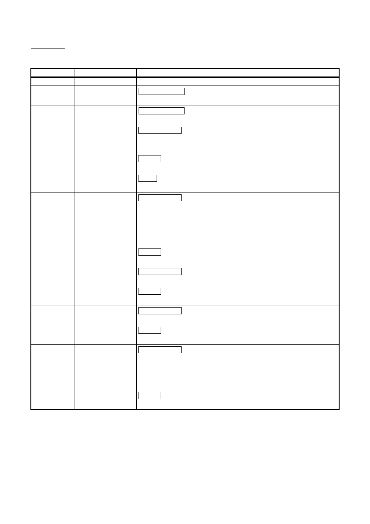
REVISIONS
Addition of model
Addition of model
Partial correction
Addition
Partial correction
Addition
Partial correction
Addition
Partial correction
Addition
Partial correction
Addition
The manual number is given on the bottom left of the back cover.
Print Date *Manual Number Revision
Dec., 1999 SH (NA) 080065-A First printing
Mar., 2000 SH (NA) 080065-B
QA1S33B
Dec., 2003 SH (NA) 080065-C
A1SY42P
About Manual, Section 2.2.1, 2.3, 3.1, 4.1.3, 6.1, 6.3, 7.2, 8.1.3, 9.1.2, 9.1.4,
9.1.5, 9.1.6, 9.2, 9.6, 11.3, 11.4.1, Appendix 2.1, 2.3, 4, 5.3
Appendix 6
Delete
Appendix 5 List of Instruction Processing Time
Oct., 2006 SH (NA) 080065-D
SAFETY PRECAUTIONS, Section 1.1, 2.2.1, 2.2.3, 2.3, Chapter 3, Section 3.1,
4.1, 4.1.1, 4.1.3, 4.1.4, 4.2.1, 4.2.2, 4.2.3, 4.2.6, 4.3, 4.4.1, 4.5, 4.6.1, 4.6.3, 5.1,
5.2, 6.1.1, 6.2, 7.2.1, 7.3, 7.7, 7.7.1, 7.7.2, Chapter 8, Section 8.1.3, 8.2.4, 8.2.6,
9.1.1, 9.1.2, 9.1.3, 9.1.4, 9.2, 9.2.4, 9.5, 9.5.1, 9.5.2, 10.3, 10.4, 11.2.8, 11.3.2,
11.4.1, Appendix 2.1, 2.3, 4.1, WARRANTY
May, 2007 SH (NA) 080065-E
Oct., 2008 SH (NA) 080065-F
Mar., 2010 SH (NA) 080065-G
Section 9.5.1, 9.5.2, 11.2.10
Section 2.3, 8.1.3, 8.2.7, 9.5.1, 9.5.2, 11.4.2
Section 8.1.7
SAFETY PRECAUTIONS, Chapter 3, Section 4.2.2, 5.1, 7.2.1, 7.7, 9.5.1, 11.4.1
Appendix 7, 7.1, 7.2
"PLC" was changed to "programmable controller".
SAFETY PRECAUTIONS, Section 2.2.1, 2.3, 4.1, 4.2.6, 4.4.3, 4.6.1, 5.1, 7.6,
7.7.2, Chapter 8, Section 9.1.2, 9.2, 9.5.1, 11.3.2, 11.4.1, Appendix 2.1, 2.2, 4.1,
5.1, 6.1, WARRANTY
CONDITIONS OF USE FOR THE PRODUCT
A - 10
Page 13
The manual number is given on the bottom left of the back cover.
Partial correction
Addition
Partial correction
Addition
Partial correction
Partial correction
Partial correction
Partial correction
Partial correction
Print Date *Manual Number Revision
Jan., 2011 SH (NA) 080065-H
Section 4.1.4, 8.8, Chapter 9, Section 9.1, 9.1.1, 9.1.2, 9.1.3, 9.1.4, 9.1.5, 9.1.6,
Section 9.1.7, 9.1.8
Oct., 2011 SH (NA) 080065-I
Introduction, Section 2.1, 2.3, 2.4.1, Chapter 3, Section 4.5, 6.1.1, 6.1.2, 6.2,
8.1.1, 9.1.1, 9.1.2, 9.1.3, 9.3, 9.5.1, Chapter 10, Section 11.2.4, 11.2.5, 11.2.6,
11.2.7, 11.2.8, 11.2.9, 11.2.10, Appendix 2.1, 2.2, 5.2, 5.3
Section 6.4
Apr., 2012 SH (NA) 080065-J
USER PRECAUTIONS, Chapter 3, Chapter 7, Section 10.3, 10.4, 11.3.2
Feb., 2015 SH(NA)-080065-K
Chapter 3, Section 4.6.1, 5.1, 5.2, 7.2.1, 7.7.2, 8.1.3, 8.2.6, 9.5.2, Appendix 5.1
Dec., 2015 SH(NA)-080065-L
Section 2.1, 7.4, Appendix 5.3, WARRANTY
Dec., 2017 SH(NA)-080065-M
Jun., 2019 SH(NA)-080065-N
Section 7.2.1
Section 2.1, 2.3, 7.1.1, 11.2.9, Appendix 6.1
This manual confers no industrial property rights or any rights of any other kind, nor dose it confer any patent licenses.
Mitsubishi Electric Corporation cannot be held responsible for any problems involving industrial property rights which may
occur as a result of using the contents noted in this manual.
Japanese Manual Version SH-080066-P
1999 MITSUBISHI ELECTRIC CORPORATION
A - 11
Page 14

Introduction
Thank you for purchasing the Mitsubishi Electric programmable controller MELSEC-Q series.
Before using your new programmable controller, please read this manual thoroughly to gain an
understanding of its functions so you can use it properly.
When applying the program examples introduced in this manual to the actual system, ensure the
applicability and confirm that it will not cause system control problems.
Please forward a copy of this manual to the end user.
Table of Contents
1 OVERVIEW 1 - 1 to 1 - 2
1.1 Features ........................................................................................................................................1 - 2
2 SYSTEM CONFIGURATION 2 - 1 to 2 - 23
2.1 System Configuration ....................................................................................................................2 - 1
2.2 Precautions When Configuring the System...................................................................................2 - 2
2.2.1 Hardware...............................................................................................................................2 - 2
2.2.2 Software package .................................................................................................................2 - 4
2.2.3 Precautions when using GPP function software packages and A8PUE peripheral devices
which are not compatible with AnU .......................................................................................2 - 7
2.3 System Equipment ........................................................................................................................2 - 8
2.4 System Configuration Overview ..................................................................................................2 - 22
2.4.1 QCPU-A system ..................................................................................................................2 - 23
3 SPECIFICATIONS 3 - 1 to 3 - 2
4 CPU MODULE 4 - 1 to 4 - 46
4.1 Performance Specifications...........................................................................................................4 - 1
4.1.1 Overview of operation processing.........................................................................................4 - 4
4.1.2 Operation processing of RUN, STOP, PAUSE, and STEP-RUN..........................................4 - 7
4.1.3 Operation processing upon instantaneous power failure ......................................................4 - 9
4.1.4 Self-diagnostics functions ...................................................................................................4 - 10
4.1.5 Device list ............................................................................................................................4 - 13
4.2 Parameter Setting Ranges ..........................................................................................................4 - 15
4.2.1 List of parameter setting range ...........................................................................................4 - 15
4.2.2 Memory capacity setting (for main program, file register, comment, etc.) ..........................4 - 18
4.2.3 Setting ranges of timer and counter ....................................................................................4 - 22
4.2.4 I/O devices ..........................................................................................................................4 - 24
4.2.5 I/O assignment of special function module .........................................................................4 - 25
4.2.6 MELSECNET/MINI-S3 auto refresh processing .................................................................4 - 26
4.3 Function List ................................................................................................................................4 - 31
4.4 Functions added to QCPU-A .......................................................................................................4 - 33
4.4.1 Boot operation from built-in ROM........................................................................................4 - 33
4.4.2 Usage of 1ms timer .............................................................................................................4 - 36
4.4.3 Sequence accumulation time processing............................................................................4 - 39
A - 12
Page 15

4.5 Handling Precautions ..................................................................................................................4 - 41
4.6 Part Names and Settings ............................................................................................................4 - 43
4.6.1 Part names..........................................................................................................................4 - 43
4.6.2 Switch operation after program write ..................................................................................4 - 46
4.6.3 Latch clear operation...........................................................................................................4 - 46
4.6.4 Handling of the memory card at power-on ..........................................................................4 - 46
5 POWER SUPPLY MODULE 5 - 1 to 5 - 4
5.1 Specifications ................................................................................................................................5 - 1
5.2 Part Names ...................................................................................................................................5 - 3
6 BASE UNIT AND EXTENSION CABLE 6 - 1 to 6 - 8
6.1 Specifications ................................................................................................................................6 - 1
6.1.1 Base unit specifications.........................................................................................................6 - 1
6.1.2 Extension cables specifications ............................................................................................6 - 2
6.2 Part Names and Settings ..............................................................................................................6 - 3
6.3 Setting the Extension Stage Numbers ..........................................................................................6 - 6
6.4 Voltage drop when an extension base unit is used .......................................................................6 - 7
7 MEMORY CARD AND BATTERY 7 - 1 to 7 - 13
7.1 Memory Card.................................................................................................................................7 - 1
7.1.1 Specifications ........................................................................................................................7 - 1
7.2 Battery Specifications (CPU Module and Memory Card Batteries) ...............................................7 - 2
7.2.1 Specifications ........................................................................................................................7 - 2
7.2.2 Handling precautions ............................................................................................................7 - 3
7.3 Handling Memory Cards................................................................................................................7 - 4
7.4 Part Names of Memory Card.........................................................................................................7 - 5
7.5 Installing/Removing a Memory Card .............................................................................................7 - 6
7.6 Installing Batteries (CPU Module and Memory Card Batteries) ....................................................7 - 7
7.7 Battery Replacement.....................................................................................................................7 - 8
7.7.1 Battery life .............................................................................................................................7 - 9
7.7.2 Battery replacement procedure...........................................................................................7 - 11
8 EMC AND LOW VOLTAGE DIRECTIVES 8 - 1 to 8 - 15
8.1 Requirements for Compliance with EMC Directive .......................................................................8 - 1
8.1.1 EMC Directive related standards ..........................................................................................8 - 2
8.1.2 Installation inside the control panel .......................................................................................8 - 3
8.1.3 Cable.....................................................................................................................................8 - 4
8.1.4 Power supply module ............................................................................................................8 - 9
8.1.5 Ferrite core..........................................................................................................................8 - 10
8.1.6 Noise filter (power supply line filter) ....................................................................................8 - 10
8.1.7 Power line for external power supply terminal ....................................................................8 - 11
8.1.8 Installation environment of the CC-Link/LT module and the AS-i module...........................8 - 11
8.2 Requirements for Compliance with Low Voltage Directive..........................................................8 - 12
8.2.1 Standard applied for MELSEC-AnS series programmable controller .................................8 - 12
8.2.2 Precautions when using the MELSEC-AnS series programmable controller......................8 - 12
A - 13
Page 16

8.2.3 Supply power ......................................................................................................................8 - 13
8.2.4 Control panel.......................................................................................................................8 - 14
8.2.5 Module installation ..............................................................................................................8 - 15
8.2.6 External wiring.....................................................................................................................8 - 15
9 LOADING AND INSTALLATION 9 - 1 to 9 - 30
9.1 Module Installation ........................................................................................................................9 - 1
9.1.1 Handling precautions ............................................................................................................9 - 1
9.1.2 Precautions on base unit installation.....................................................................................9 - 2
9.1.3 Installation and removal of the dustproof cover ....................................................................9 - 5
9.1.4 Installation and removal of modules......................................................................................9 - 7
9.1.5 Extension stage number setting for the extension base unit...............................................9 - 11
9.1.6 Connecting/disconnecting the extension cable ...................................................................9 - 12
9.2 Concept of Fail Safe Circuit.........................................................................................................9 - 15
9.3 Installation Environment ..............................................................................................................9 - 21
9.4 Calculation Method of Heat Amount Generated by the Programmable Controller......................9 - 22
9.5 Wiring ..........................................................................................................................................9 - 24
9.5.1 Wiring precautions ..............................................................................................................9 - 24
9.5.2 Wiring to module terminals..................................................................................................9 - 29
9.6 Precautions when Connecting the Uninterruptible Power Supply (UPS) ....................................9 - 30
10 MAINTENANCE AND INSPECTION 10 - 1 to 10 - 5
10.1 Daily Inspection ...........................................................................................................................10 - 2
10.2 Periodic Inspection ......................................................................................................................10 - 3
10.3 Operating a CPU Module After Being Stored Without a Battery .................................................10 - 4
10.4 Operating a CPU Module After Being Stored Over the Battery Life............................................10 - 5
11 TROUBLESHOOTING 11 - 1 to 11 - 27
11.1 Fundamentals of Troubleshooting...............................................................................................11 - 1
11.2 Troubleshooting...........................................................................................................................11 - 2
11.2.1 Troubleshooting flowchart ...................................................................................................11 - 2
11.2.2 Flow for actions when the POWER LED is turned off .........................................................11 - 3
11.2.3 Flow for actions when the MODE LED turns off..................................................................11 - 4
11.2.4 Flow for actions when the RUN LED is turned off...............................................................11 - 5
11.2.5 Flow for actions when the RUN LED is flashing..................................................................11 - 6
11.2.6 Flow for actions when the ERR. LED is turned on ..............................................................11 - 7
11.2.7 Flow for actions when the ERR. LED is flashing .................................................................11 - 8
11.2.8 Flow for actions when the output module's output load does not turn on ...........................11 - 9
11.2.9 Flow for actions when the program cannot be written.......................................................11 - 10
11.2.10 Flow for actions when the CPU module is not started up ................................................11 - 11
11.3 Error Code List ..........................................................................................................................11 - 12
11.3.1 Procedure to read an error code .......................................................................................11 - 12
11.3.2 Error code list for the QCPU-A (A Mode) ..........................................................................11 - 13
11.4 Fault Examples with I/O Modules ..............................................................................................11 - 22
11.4.1 Faults with the input circuit and the corrective actions ......................................................11 - 22
11.4.2 Faults in the output circuit .................................................................................................11 - 24
A - 14
Page 17

APPENDICES Appendix - 1 to Appendix - 61
Appendix 1 Instruction List .............................................................................................................. App - 1
Appendix 1.1 Precautions for write during RUN of a dedicated instruction ............................ App - 14
Appendix 2 Lists of Special Relays and Special Registers .......................................................... App - 15
Appendix 2.1 Special relays................................................................................................... App - 15
Appendix 2.2 Special Registers ............................................................................................. App - 27
Appendix 3 Peripheral Device....................................................................................................... App - 46
Appendix 4 Precautions for Utilizing the Existing Sequence Programs for the QCPU-A.............. App - 48
Appendix 4.1 Instructions with different specifications............................................................ App - 49
Appendix 4.2 Special relays and special registers with different specifications...................... App - 50
Appendix 4.3 Parameter setting.............................................................................................. App - 50
Appendix 4.4 I/O control mode ............................................................................................... App - 51
Appendix 4.5 Microcomputer program .................................................................................... App - 52
Appendix 4.6 Index register processing.................................................................................. App - 53
Appendix 5 External Dimensions .................................................................................................. App - 54
Appendix 5.1 Q02CPU-A, Q02HCPU-A and Q06HCPU-A QCPU-A module ......................... App - 54
Appendix 5.2 A1S61PN, A1S62PN and A1S63P power supply module ................................ App - 55
Appendix 5.3 Base unit ........................................................................................................... App - 56
Appendix 6 Transportation Precautions ........................................................................................ App - 58
Appendix 6.1 Relevant models ............................................................................................... App - 58
Appendix 6.2 Transportation Guidelines................................................................................. App - 59
Appendix 7 Handling of Batteries and Devices with Built-in Batteries in EU Member States ....... App - 60
Appendix 7.1 Disposal precautions......................................................................................... App - 60
Appendix 7.2 Exportation precautions .................................................................................... App - 61
INDEX Index - 1 to Index - 3
A - 15
Page 18

About This Manual
Related manuals
The following manuals are related to this product.
Manual Name
ACPU/QCPU-A (A mode) Programming Manual (Fundamentals)
Describes programming methods necessary for creating programs, device names, parameters,
program types, memory area configuration, and so on. (Sold separately)
ACPU/QCPU-A (A mode) Programming Manual (Common Instructions)
Describes how to use the sequence instruction, basic instructions, applied instructions and
microcomputer programs. (Sold separately)
AnSHCPU/AnACPU/AnUCPU/QCPU-A (A mode) Programming Manual (Dedicated Instructions)
Describes instructions that have been expanded.
(Sold separately)
AnACPU/AnUCPU/QCPU-A (A mode) Programming Manual (PID Instructions)
Describes dedicated instructions to perform the PID control. (Sold separately)
AnS Module type I/O User's Manual
Describes the specification of the compact building block type I/O module. (Sold separately)
Manual No.
(Model Code)
IB-66249
(13J740)
IB-66250
(13J741)
IB-66251
(13J742)
IB-66258
(13J744)
IB-66541
(13JE81)
A - 16
Page 19

USER PRECAUTIONS
Precautions for using a CPU module
When a CPU module is used for the first time, data in the CPU module (built-in RAM, device
data) and in the memory card are undefined.
Before writing data (parameters, programs) to the CPU module, clear data in the built-in RAM
using a peripheral (PC memory clear operation) and also clear data using the RESET/L.CLR
switch of the CPU module (latch clear operation).
Precautions for battery
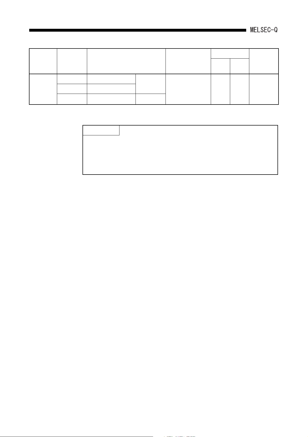
(1) Operating a CPU module after being stored without a battery
When a CPU module is operated again after being stored without a battery, data in the
CPU module (built-in RAM, device data) and a memory card may be undefined.
Before operating the CPU module again, clear data in the built-in RAM using a
peripheral (PC memory clear operation) and also clear data using the RESET/L.CLR
switch of the CPU module (latch clear operation).*
After all data are cleared, write the backed-up data in the CPU module or the memory
card.
(2) Operating a CPU module after being stored over the battery life
When a CPU module is operated again after being stored over the battery life, data in
the CPU module (built-in RAM, device data) and a memory card may be undefined.
Before operating the CPU module again, clear data in the built-in RAM using a
peripheral (PC memory clear operation) and also clear data using the RESET/L.CLR
switch of the CPU module (latch clear operation).*
After all data are cleared, write the backed-up data in the CPU module or the memory
card.
POINT
Make sure to back up each memory contents before storing the programmable
controller.
* For details of the PC memory clear operation using a peripheral, refer to the following manuals.
GX Developer Operating Manual
A6GPP/A6PHP Operating Manual
SW IVD-GPPA Operating Manual
For the latch clear operation using the RESET/L.CLR switch of the CPU module, refer to Section
4.6.3.
A - 17
Page 20
1. OVERVIEW
1 OVERVIEW
This user's manual describes the performance, functions, and handling method of the
QCPU-A, as well as the specifications and handling of the memory card, power supply
module and the base unit.
The programming modules and software packages have to be compatible with the
upgraded A2UCPU, A2UCPU-S1, A3UCPU, and A4UCPU (abbreviated as AnUCPU
hereafter).
When the conventional programming modules and software packages are used, the
usable range varies depending on the model of the CPU (programmable controller model
name).(Refer to Section 2.2.3.)
Related to each module used in the CPU modules, check "System equipment list" in
Section 2.3.
Refer to Section 2.2.1 for the special function modules which have limited usable devices
range.
(1) Bundled parts
Product Name Model Quantity
CPU module
Battery Q6BAT 1
Q02CPU-A
1Q02HCPU-A
Q06HCPU-A
1 - 1
Page 21
OVERVIEW1.
1.1 Features
QCPU-A (A mode) has the following features compared with A2USHCPU-S1.
(1) High-speed operation processing speed
QCPU-A offers significantly higher operation processing than that of A2USHCPU-S1.
Item Q02CPU-A
Operation processing
1
*
speed
*1 I/O processing: At refresh or LD instruction
79ns 34ns 90ns
Q02HCPU-A,
Q06HCPU-A
A2USHCPU-S1
(2) Greater program capacity
By using Q06HCPU-A, the program capacity can be expanded.
Moreover, Q06HCPU-A can create subprograms.
Item Q06HCPU-A A2USHCPU-S1
30k steps (Main program)
Program capacity
30k steps (Subprogram)
+
30k steps
(3) Increased actual I/O points
QCPU-A offers 4096 actual I/O points, 4 times as increased as that of A2USHCPUS1.
Item
Actual I/O points 4096 points 1024 points
Q02CPU-A, Q02HCPU-A,
Q06HCPU-A
A2USHCPU-S1
(4) Increased extension stages
Up to 7 stages of extension base unit can be added.
(5) Higher communication speed with peripheral devices
The communication speed with peripheral devices is considerably improved
compared with A2USHCPU-S1.
Item
Communication speed
(kbps)
* 1 Designate 9.6kbps when using GPP of SW3D5C-GPPW or earlier.
Q02CPU-A, Q02HCPU-A,
Q06HCPU-A
1
*
115 .2
A2USHCPU-S1
9.6
1 - 2
Page 22
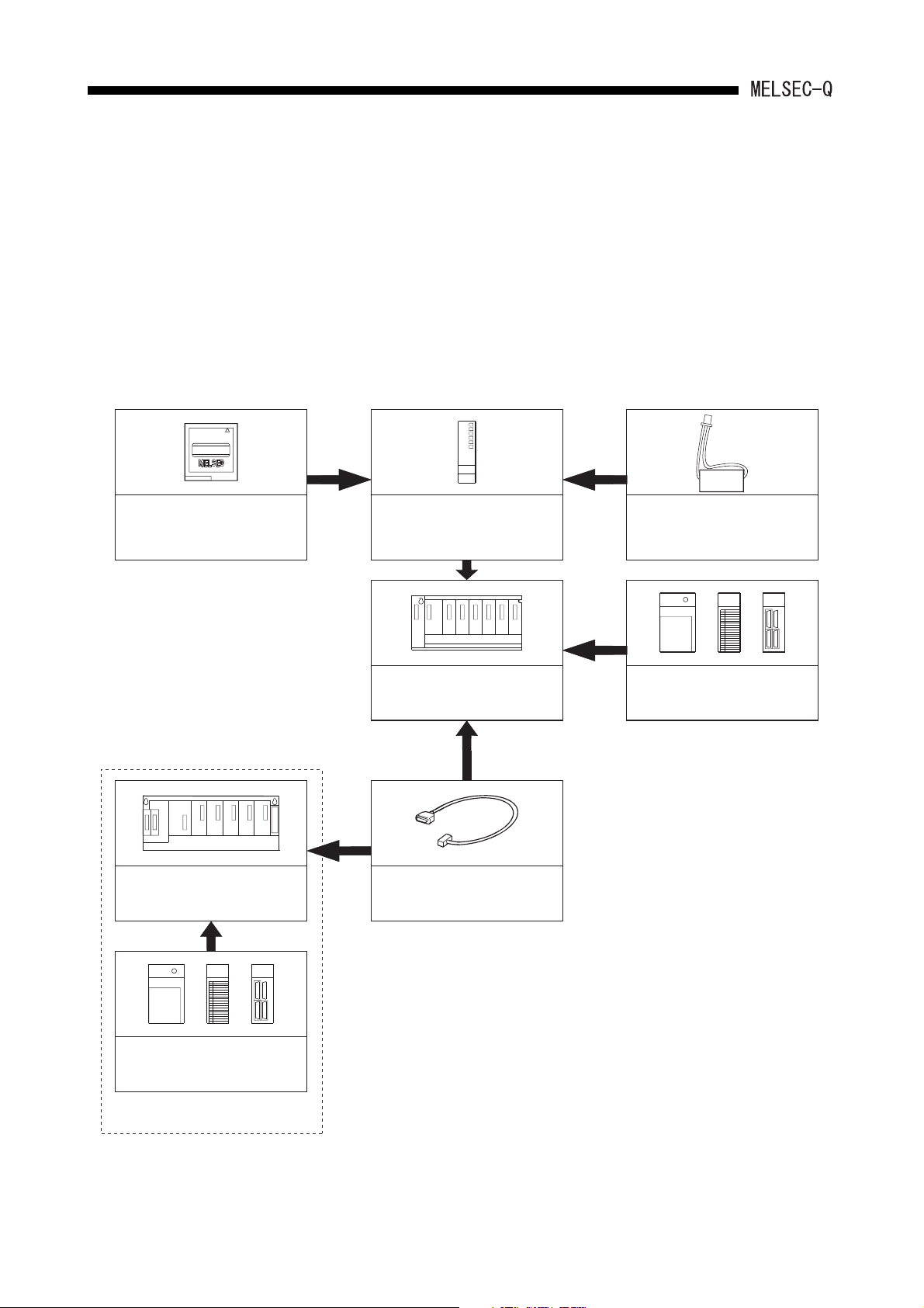
2. SYSTEM CONFIGURATION
LITHIUM BATTERY
QCPU-A
(Q02CPU-A, Q02HCPU-A,
Q06HCPU-A)
Battery
(Q6BAT)
Main base unit
(QA1S33B,QA1S35B,QA1S38B)
Extension cable
(QC05B,QC06B,QC12B,
QC30B,QC50B,QC100B)
Extension base unit
(QA1S51B,QA1S65B,QA1S68B)
Expansion of AnS series modules
*1
AnS series power supply
*2
, I/O,
or special function modules
The operation is not guaranteed
for the use of commercially
available memory cards.
*2
The power supply module cannot
be mounted on the QA1S51B.
Q series power supply, I/O, or
intelligent function modules
Memory card
*1
(Q2MEM-1MBSN,
Q2MEM-1MBS)
2 SYSTEM CONFIGURATION
This chapter shows the system configuration of QCPU-A, the relevant precautions and
system equipment.
2.1 System Configuration
This section describes the configuration of the QCPU-A system, the configuration of
peripheral devices, and the overview of the system configuration.
(1) Configuration of the QCPU-A system
2 - 1
Page 23
2. SYSTEM CONFIGURATION
2.2 Precautions When Configuring the System
The following shows the precautions when configuring the QCPU-A system:
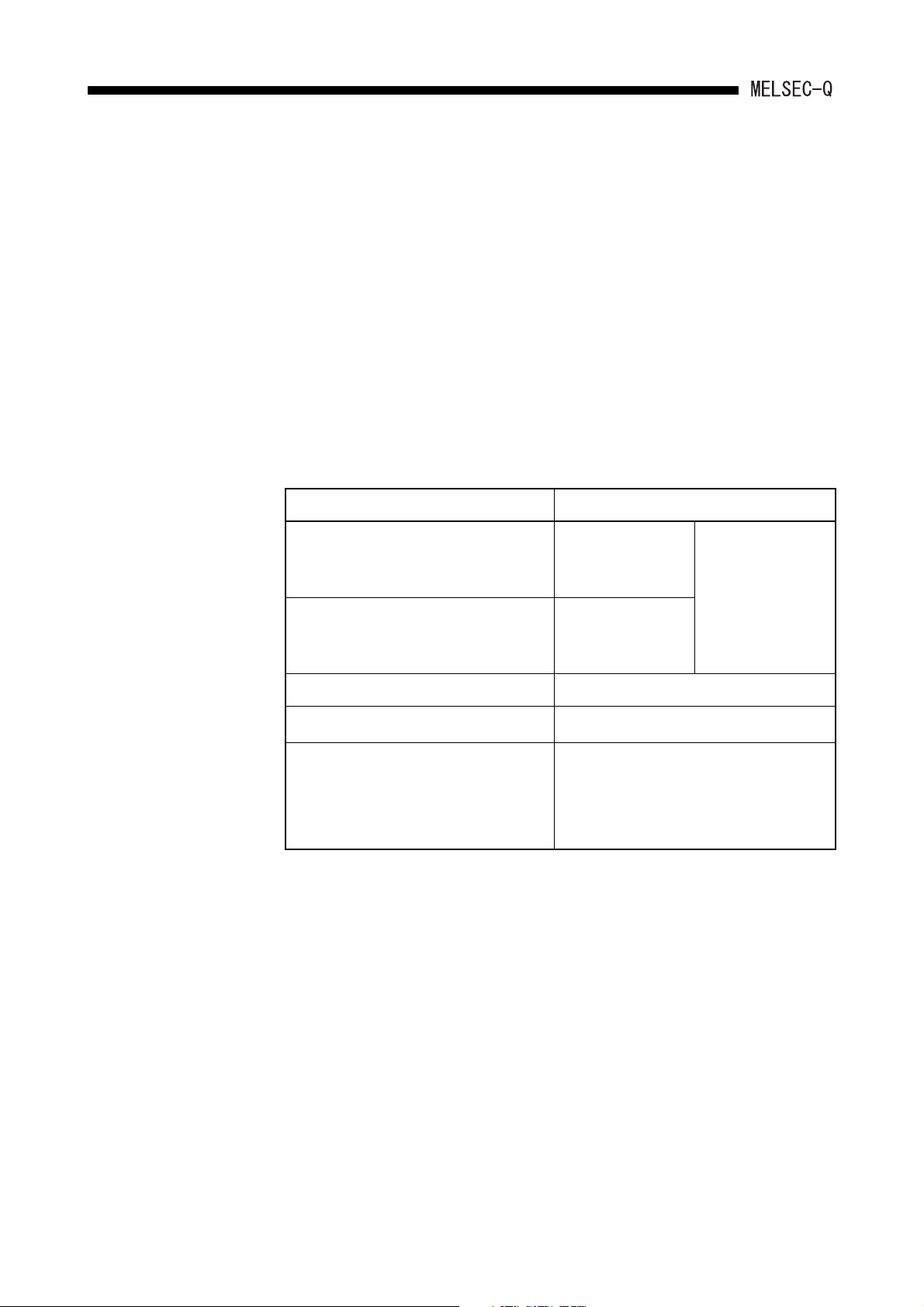
2.2.1 Hardware
(1) Up to 64 I/O modules or special function modules can be mounted to each of the
basic base unit or the extension base unit.
(2) Up to 7 extension base units can be connected in the system.
(Up to 8 modules including the main base unit.)
(3) The total length of the extension cable should be 13.2m or less.
(4) The following shows the modules that have some limitations for the number of
modules to be mounted.
Module No. of Mountable Modules
MELSECNET/10 network module
A1SJ71LP21(GE), A1SJ71LR21,
A1SJ71BR11
MELSECNET(II)/B data link module
A1SJ71AP21, A1SJ71AR21,
Up to 4 modules
Up to 4 modules in
total
Up to 2 modules
A1SJ71AT21B
Interruption module: A1SI61 1 module
AnS series special function module
*
Up to 6 modules in total
1
GOT-A900 Series (Only when the bus
2
connection is used.)
GOT1000 Series (Only when the bus
connection is used.)
*1 Applies to the following modules. Any modules but the following modules do not have the
number of limitations to be mounted.
Ethernet interface module: A1SJ71E71N-B2 (-B5/-T)
Calculating machine link module: A1SJ71UC24-R2 (-R4/-PRF)
CC-Link module (in intelligent mode): A1SJ61BT11
Intelligent communication module: A1SD35ID1(2)
ID interface module: A1SD35ID1(2)
*2 Refer to the following manual for the GOT models.
• GOT-A900 Series User's Manual (GT Works Versions2/GT Designer2 Version2 Compatible
Connection System Manual)
• GOT1000 Series Connection Manual (Mitsubishi Products)
*
Connection disable
2
*
2 - 2
Page 24
SYSTEM CONFIGURATION2.
(5) The accessible device ranges have limit when the following modules are used:
Accessible Device Range in CPU
Applicable Module
Device Accessible Range
Input (X), output (Y) X/Y0 to X/Y7FF
Internal relay (M) M0 to M8191
latch relay (L) L0 to L8191
MELSECNET(II) data link module:
A1SJ71AP21, A1SJ71AR21
MELSECNET/B data link module:
A1SJ71AT21B
Link relay (B) B0 to BFFF
Timer (T) T0 to T2047
Counter (C) C0 to C1023
Data register (D) D0 to D6143
Link register (W) W0 to WFFF
Annunciator (F) F0 to F2047
(6) It is recommended that the network and data link modules are mounted to the basic
base unit.
When these modules are mounted to the extension base unit, the link refresh time
becomes longer than the case where they are mounted to the basic base unit.
2 - 3
Page 25
2. SYSTEM CONFIGURATION
2.2.2 Software package
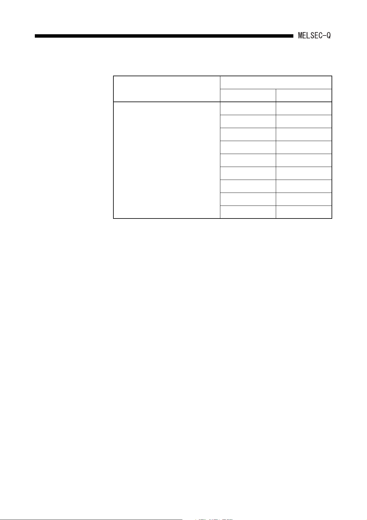
(1) GPP function software packages and model name setting at the start-up
The following table shows the GPP function software package that can be used to
create the QCPU-A program, and the programmable controller type setting at startup.
When using SW4D5C-GPPW or later, select the programmable controller type from
Q02(H)-A or Q06H-A according to the CPU to be used.
When using the peripheral devices and GPP function software package of SW3D5CGPPW or earlier, specify the programmable controller type name as "A4U". If "A4U"
is not found in PLC type names, specify "A3A." If both "A4U" and "A3A" are not
found, specify "A3H."
Note that when "A4U" is specified, the available device range is limited.
Peripheral
device
Software package for system start-up
Programmable controller CPU
model setting
Q02(H)-A Q06H-A
PC/AT
personal
computer
A6PHP SW3GP-GPPA A3H A3H
A6GPP SW3-GPPA
SW4D5C-GPPW or later Q02(H)-A Q06H-A
SW3D5 -GPPW or earlier
A4U A4U
SW IVD-GPPA
SW4GP-GPPA A3A A3A
SW1GP-GPPAU A4U A4U
SW3GP-GPPA
SW4GP-GPPA A3A A3A
SW1GP-GPPAU A4U A4U
A3H A3H
2 - 4
Page 26

SYSTEM CONFIGURATION2.
POINT
(1) Old software packages other than listed above cannot be used.
(2) To construct MELSECNET/10 network system with QCPU-A, use the AnU-
compatible GPP function software package (which includes "A4U" in its
programmable controller type name).
A network cannot be constructed with the GPP function software package
which is not compatible with AnU (which does not include "A4U" in its
programmable controller type name).
(3) Communication with GX Developer at 115.2kbps may not be available
depending on the peripheral devices. In such a case, select the lower
communication speed.
(4) When using Q02(H)CPU-A and conventional peripheral devices and setting
the programmable controller type as "A4U," designate the main program
setting to 28k steps or less with parameters. When "Main + parameter" is
written with the programmable controller with the setting of 29k steps or more,
"Cannot communicate with PC" is displayed, and writing to the CPU module is
disabled.
(5) Subprograms cannot be used with Q02(H)CPU-A. When using conventional
peripheral devices and setting the programmable controller type as "A4U," do
not specify any subprograms. If any subprograms are specified, "Cannot
communicate with PC" is displayed.
With Q06HCPU, subprogram 1 can be used, but subprograms 2 and 3
cannot.
When subprogram 2 or 3 is specified, the same message above is displayed.
2 - 5
Page 27

SYSTEM CONFIGURATION2.
(2) Utility package
(a) None of the following utility packages for A6GPP/A6PHP can be used:
The packages marked with * can
•SW -AD57P
• SW -UTLP-FN0
• SW -UTLP-FN1
•SW -UTLP-PID
•SW -SIMA
• SW -UTLP-FD1
•SW -SAPA
POINT
*
(1) The utility package, which specifies the device and accesses the QCPU-A,
can be used only in the device range for the A3ACPU, A3HCPU equivalent.
(Refer to Section 2.2.3.)
(2) Use an AnU-compatible utility package to use the device range for the
QCPU-A.
(Example: SW1IVD-SAP2, etc.)
*
execute the same functions using the
dedicated instructions.
For details, refer to type AnSHCPU/
AnACPU/AnUCPU/QCPU-A (A Mode)
Programming Manual (Dedicated
Instructions).
2 - 6
Page 28
2. SYSTEM CONFIGURATION
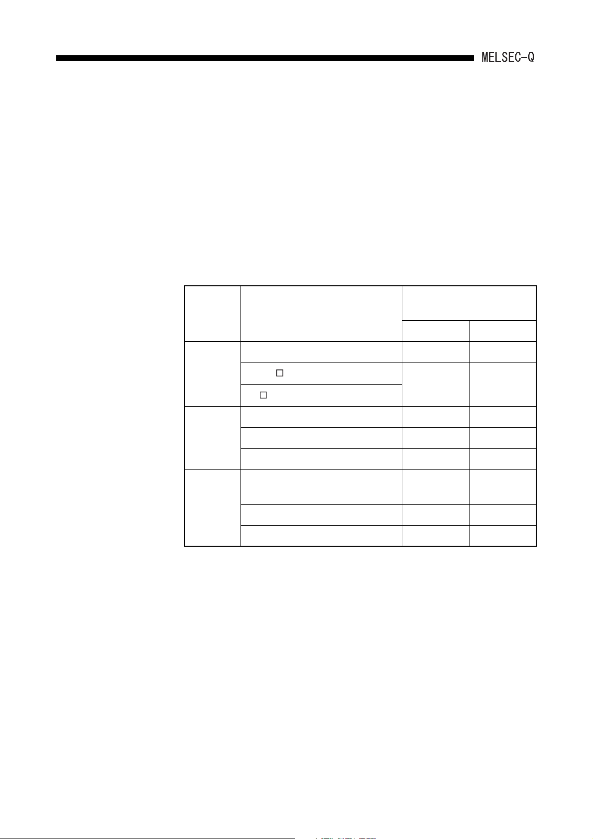
2.2.3 Precautions when using GPP function software packages and A8PUE peripheral devices which are not compatible with AnU
When starting with GPP function software packages not compatible with the AnU, QCPUA (starting with the programmable controller model name "A3A" or "A3H") or a A8PUE
peripheral device (including A7PUS), the usable device ranges are limited as follows.
(1) List of usable device range
AnACPU-compatible Module A3HCPU-compatible Module
Item
Instruction (sequence/basic/
application/dedicated)
Program capacity Max. 14k steps can be used for the main program.
I/O device points (X/Y)
M, L, S relay M/L/S0 to M/L/S8191 can be used.
Link relay (B)
Timer (T) T0 to T2047 can be used.
Counter (C) C0 to C1023 can be used.
Data register (D)
Programmable controller Model
"A3A"
at System FD Start-up
X/Y0 to X/Y7FF can be used.
(X/Y800 to X/Y1FFF cannot be used.)
B0 to BFFF can be used.
(B1000 to B1FFF cannot be used.)
D0 to D6143 can be used.
(D6144 to D8191 cannot be used.)
A8PUE
All instructions can be used.
Programmable controller Model
"A3H"
at System FD Start-up
X/Y0 to X/Y7FF can be used.
(X/Y800 to X/Y1FFF cannot be used.)
M/L/S0 to M/L/S2047 can be used.
(M/L/S2048 to M/L/S8191 cannot be used.)
B0 to B3FF can be used.
(B400 to B1FFF cannot be used.)
T0 to T255 can be used.
(T256 to T2047 cannot be used.)
C0 to C255 can be used.
(C256 to C1023 cannot be used.)
D0 to D1023 can be used.
(D1024 to D8191 cannot be used.)
A7PUS
Link register (W)
Annunciator (F) F0 to F2047 can be used.
Index register (V, Z) V, V1 to V6, Z, Z1 to Z6can be used.
Expanded comment Max. 3968 points – Unusable –
Latch (power failure compensation)
range
I/O assignment
The device range shown above can be latched. The device range shown above can be latched.
Possible to register occupied I/O
points and module model names.
W0 to WFFF can be used.
(W1000 to W1FFF cannot be used.)
Number of I/O occupied points can
–
W0 to W3FF can be used.
(W400 to W1FFF cannot be used.)
F0 to F255 can be used.
(F256 to F2047 cannot be used.)
V and Z can be used.
(V1 to V6, Z1 to Z6 cannot be used.)
be registered.
(1) The device range other than listed above is the same as that of QCPU-A.
(2) Refer to Operating Manual for peripheral devices to be used for available functions.
2 - 7
–
Page 29

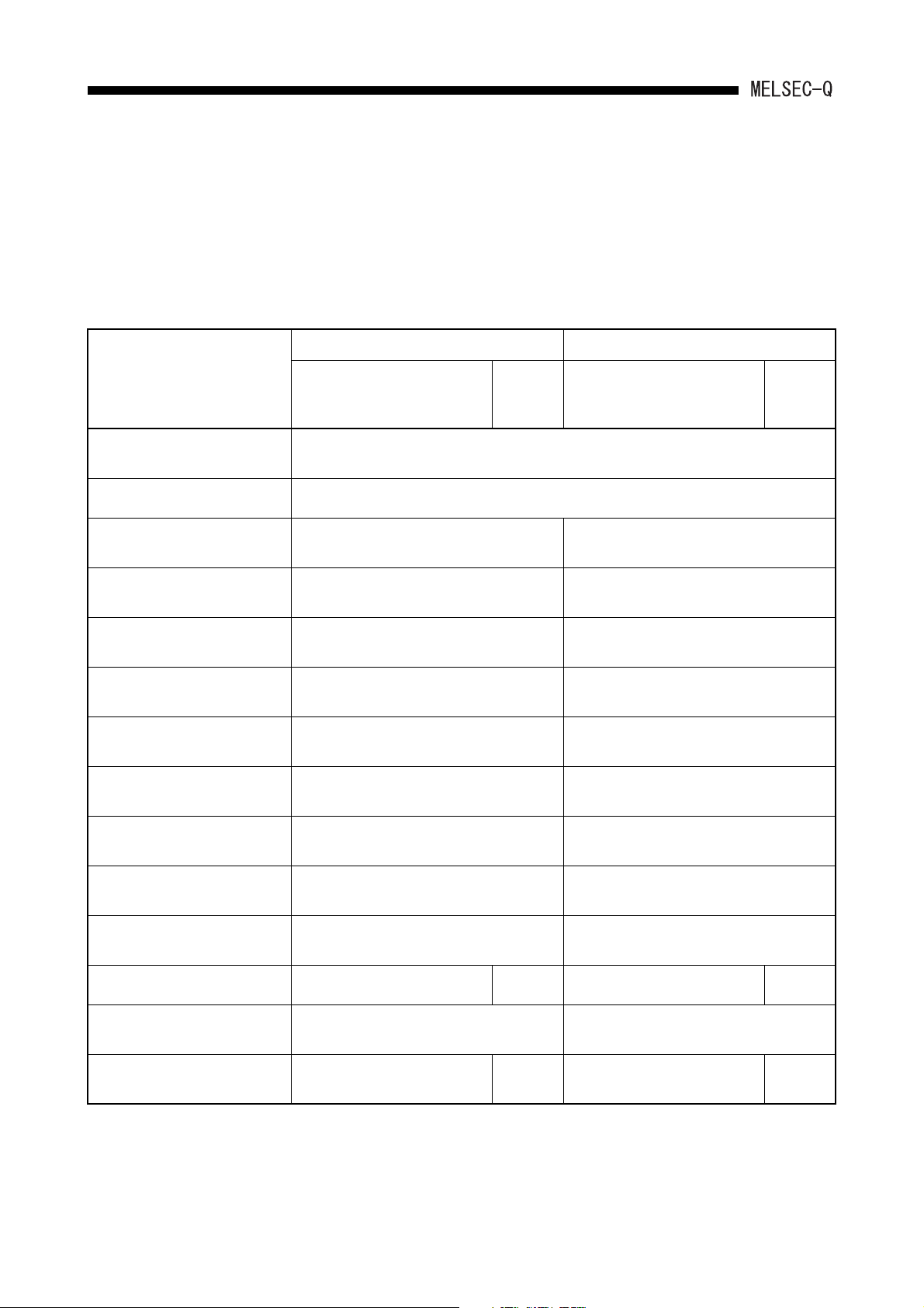
2. SYSTEM CONFIGURATION
2.3 System Equipment
The following shows various components of each module and peripheral device which can
be used by the QCPU-A.
(1) Modules dedicated to AnS
Product Name Model Name Description
Program capacity: 28k steps, I/O points: 4096,
Processing speed for basic instruction: 79ns
Program capacity: 28k steps, I/O points: 4096,
Processing speed for basic instruction: 34ns
Program capacity: 30k steps 2 (Main/sub),
I/O points: 4096, Processing speed for basic
instruction: 34ns
SRAM type: 1MB – – –
AnS series module mounting base (power
supply module + CPU module + 3 slots for other
module)
AnS series module mounting base (power
supply module + CPU module + 5 slots for other
module)
AnS series module mounting base (power
supply module + CPU module + 8 slots for other
module)
CPU module
Memory card
Main base unit
Q02CPU-A
Q02HCPU-A
Q06HCPU-A
Q2MEM-1MBSN,
Q2MEM-1MBS
QA1S33B
QA1S35B
QA1S38B
Number of Occupied
Points (points)
[I/O Assignment
Module Type]
–0.60–
–0.64–
–0.64–
– 0.107 –
–
–
Current Consumption
5VDC(A) 24VDC(A)
0.117
(0.086)*
0.118
(0.086)*
–
–
Remark
QA1S51B
Extension base
unit
Extension cable
Battery Q6BAT
Cable QC30R2 Communication cable for peripheral devices – – –
QA1S65B
QA1S68B
QC05B 0.45m extension base cable – – –
QC06B 0.6m extension base cable – – –
QC12B 1.2m extension base cable – – –
QC30B 3.0m extension base cable – – –
QC50B 5.0m extension base cable – – –
QC100B 10.0m extension base cable – – –
AnS series module mounting base, 1 slot for
other module
AnS series module mounting base (power
supply module + CPU module + 5 slots for other
module)
AnS series module mounting base (power
supply module + CPU module + 8 slots for other
module)
Battery for retaining the contents of built-in RAM
and devices in case of power failure
–0.12–
–
–
–––
0.117
(0.088)*
0.118
(0.090)*
–
–
2 - 8
Page 30
SYSTEM CONFIGURATION2.
POINT
(1) A USB port cannot be used with QCPU-A.
(2) A RS232/422 conversion cable is required to use the conventional peripheral
devices (A6GPP, A8PUE, etc.).
Recommended cable: FA-CNV2402CBL (2m), FA-CNV2405CBL (5m)
Contact: Mitsubishi Electric Engineering Corp.
Product Name Model Name Description
A1S61PN 5VDC, 5A
Power supply
module
A1S62PN 5VDC, A/24VDC, 0.6A
A1S63P 5VDC, 5A 24VDC input
* The parenthesized values are for those which is not compliant with CE.
100/200VAC
input
Number of Occupied
Points (points)
[I/O Assignment
Module Type]
–––
Current Consumption
Remark
5VDC(A) 24VDC(A)
Installed in the
power supply
slot of the main
base and
extension base.
2 - 9
Page 31

SYSTEM CONFIGURATION2.
Product Name Model Name Description
A1SX10 16-point 100 to 120 VAC input module 16 [16 input points] 0.05 –
A1SX10EU 16-point 100 to 120 VAC input module 16 [16 input points] 0.05 –
A1SX20 16-point 200 to 240 VAC input module 16 [16 input points] 0.05 –
A1SX20EU 16-point 200 to 240 VAC input module 16 [16 input points] 0.05 –
A1SX30 16-point 12/24VDC, 12/24VAC input module 16 [16 input points] 0.05 –
A1SX40 16-point 12/24VDC input module 16 [16 input points] 0.05 –
A1SX40-S1 16-point 24VDC input module 16 [16 input points] 0.05 –
A1SX40-S2 16-point 24VDC input module 16 [16 input points] 0.05 –
A1SX41 32-point 12/24VDC input module 32 [32 input points] 0.08 –
A1SX41-S1 32-point 24VDC input module 32 [32 input points] 0.12 –
Input module
A1SX41-S2 32-point 24VDC input module 32 [32 input points] 0.08 –
A1SX42 64-point 12/24VDC input module 64 [64 input points] 0.09 –
A1SX42-S1 64-point 24VDC input module 64 [64 input points] 0.16 –
Number of Occupied
Points (points)
[I/O Assignment
Module Type]
Current Consumption
Remark
5VDC(A) 24VDC(A)
A1SX42-S2 64-point 24VDC input module 64 [64 input points] 0.09 –
A1SX71 32-point 5/12/24VDC input module 32 [32 input points] 0.075 –
A1SX80 16-point 12/24VDC sink/source input module 16 [16 input points] 0.05 –
A1SX80-S1 16-point 24VDC sink/source input module 16 [16 input points] 0.05 –
A1SX80-S2 16-point 24VDC sink/source input module 16 [16 input points] 0.05 –
A1SX81 32-point 12/24VDC sink/source input module 16 [16 input points] 0.08 –
A1SX81-S2 32-point 24VDC sink/source input module 32 [32 input points] 0.08 –
A1SX82-S1 64-point 24VDC sink/source input module 32 [32 input points] 0.16 –
2 - 10
Page 32

SYSTEM CONFIGURATION2.
Product Name Model Name Description
A1SX10 16-point relay contact output module (2A) 16
A1SY10EU 16-point relay contact output module (2A) 16
A1SY14EU 12-point relay contact output module (2A) 16
A1SY18A
A1SY18AEU
A1SY22 16-point triac output module (0.6A) 16
A1SY28A
A1SY40
A1SY40P
8-point relay contact output module (2A) for
independent contacts
8-point relay contact output module (2A) for
independent contacts
8-point triac output module (1A)
All points independent
16-point 12/24VDC transistor output module
(0.1A) sink type
16-point 12/24VDC transistor output module
(0.1A) sink type
Number of Occupied
Points (points)
[I/O Assignment
Module Type]
[16 output
points]
[16 output
points]
[16 output
points]
16
16
16
16
16
[16 output
points]
[16 output
points]
[16 output
points]
[16 output
points]
[16 output
points]
[16 output
points]
Current Consumption
5VDC(A) 24VDC(A)
0.12 0.09
0.12 0.10
0.12 0.10
0.24 0.075
0.24 0.075
(200VAC)
0.27
0.13 –
0.27 0.008
0.08 0.011
0.002
Remark
Output module
A1SY41
A1SY41P
A1SY42
A1SY50
A1SY60
A1SY60E
A1SY68A
A1SY71
A1SY80
A1SY81
32-point 12/24VDC transistor output module
(0.1A) sink type
32-point 12/24VDC transistor output module
(0.1A) sink type
64-point 12/24VDC transistor output module
(0.1A) sink type
16-point 12/24VDC transistor output module
(0.5A) sink type
16-point 24VDC transistor output module
(2A) sink type
16-point 12/24VDC transistor output module
(2A) source type
8-point 5/12/24/48VDC
transistor output module (2A) sink/source type
All points independent
32-point 5/12VDC transistor output module
(0.016A) sink type
16-point 12/24VDC transistor output module
(0.8A) source type
32-point 12/24VDC transistor output module
(0.1A) source type
32
32
64
16
16
16
16
32
16
32
[32 output
points]
[32 output
points]
[64 output
points]
[16 output
points]
[16 output
points]
[16 output
points]
[16 output
po
ints]
[32 output
points]
[16 output
points]
[32 output
points]
0.50 0.008
0.14 0.012
0.93 0.008
0.12 0.06
0.12 0.015
0.20 0.01
0.11 –
0.40 0.15
0.12 0.02
0.50 0.008
A1SY82
64-point 12/24VDC transistor output module
(0.1A) source type
2 - 11
64
[64 output
points]
0.93 0.008
Page 33

SYSTEM CONFIGURATION2.
Specified number of points
Number of Occupied
Product Name Model Name Description
32-point 12/24VDC input module
A1SH42
I/O combined
module
Dynamic input
module
Dynamic output
module
Blank cover A1SG60 Dust-proof cover for unused slot 16 [Empty] – –
A1SH42-S1
A1SX48Y18
A1SX48Y58
A1S42X
A1S42Y
32-point 12/24VDC transistor output module
(0.1A) sink type
32-point 24VDC input module
32-point 12/24VDC transistor output module
(0.1A) sink type
8-point 24VDC input module
8-point relay contact output module (2A)
8-point 24VDC input module
8-point 12/24VDC transistor output module
(0.5A)
16/32/48/64 points
12/24VDC dynamic input module
16/32/48/64 points
12/24VDC dynamic output module
Points (points)
[I/O Assignment
Module Type]
32
32
16
16
Specified number of points
[Input
Specified number of points
[Output
Specified number of points
[32 output
points]
[32 output
points]
[16 output
points]
[16 output
points]
Current Consumption
5VDC(A) 24VDC(A)
0.50 0.008
0.50 0.008
0.085 0.045
0.06 0.06
0.08 –
]
0.18 0.055
]
Remark
Dummy module A1SG62
Pulse catch
module
Analog timer
module
Interrupt
module
High-speed
counter module
A1SP60
A1ST60
A1SI61
A1SD61
A1SD62
A1SD62D
A1SD62D-S1
16-point, 32-point, 48-point, 64-point selectable
module
Short ON-time pulse input module
(pulse with a minimum of 0.5ms) 16 input points
A module whose timer setting value can be
changed for different volumes (0.1 to 1.0s, 1 to
10s, 10 to 60s, 60 to 600s)
Analog timer 8 points
Interrupt module for specifying the interrupt
program
(16-point interrupt input)
32-bit signed binary
50kBPS, 1 channel
24-bit signed binary, 2 channel
100kPPS, DC input
transistor output (sink type)
24-bit signed binary, 2 channel
200kPPS, difference input
transistor output (sink type)
24-bit signed binary, 2 channel
200kPPS, difference input
transistor output (sink type)
Specified number of points
[Input
Specified number of points
16
16
32
32
32
32
32
[16 output
points]
[16 output
points]
[32 special
points]
[32 special
points]
[32 special
po
ints]
[32 special
points]
[32 special
points]
––
]
0.055 –
0.055 –
0.057 –
0.35 –
0.1 –
0.25 –
0.27 –
A1SD62E
24-bit signed binary, 2 channel
100kPPS, DC input
transistor output (source type)
2 - 12
32
[32 special
points]
0.1 –
Page 34

SYSTEM CONFIGURATION2.
Product Name Model Name Description
4 to 20mA/0 to 10V
4 analog channels
4 to 20mA/0 to 10V
8 analog channels
4 to 20mA/0 to 10V
2 analog output channels
-10 to 10V input
8 analog output channels
4 to 20mA input
8 analog output channels
Analog input, 2 channels, simple loop control is
allowed
1 analog output channels
Analog input, 4 channels, simple loop control is
allowed
2 analog output channels
For connecting to Pt100 (3-wire)
Temperature input, 2 channels
A/D converter
module
D/A converter
module
Analog I/O
module
A1S64AD
A1S68AD
A1S62DA
A1S68DAV
A1S68DAI
A1S63ADA
A1S66ADA
A1S62RD3
Number of Occupied
Points (points)
[I/O Assignment
Module Type]
32
32
32
32
32
32
32
32
[32 special
points]
[32 special
points]
[32 special
points]
[32 special
points]
[32 special
points]
[32 special
points]
[32 special
points]
[32 special
points]
Current Consumption
Remark
5VDC(A) 24VDC(A)
0.4 –
0.4 –
0.8 –
0.65 –
0.85 –
0.8 –
0.21 0.16
0.49 –
Temperature
control module
A1S62RD4
A1S68TD Thermocouple input, 8 channels 32
A1S62TCTT-S2
A1S62TCTTBWS2
A1S62TCRT-S2
A1S62TCRTBWS2
A1S64TCTT-S1
For connecting to Pt100 (4-wire)
Temperature input, 2 channels
Transistor output, thermocouple input
2 channels/module
PID control: ON/OFF pulse
Transistor output, thermocouple input
2 channels/module
PID control: ON/OFF pulse, wire breakage
detection function
Transistor output, platinum RTD (Resistance
Temperature Detector) input
2 channels/module
PID control: ON/OFF pulse
T
ransistor output, platinum RTD input
2 channels/module
PID control: ON/OFF pulse, wire breakage
detection function
Transistor output, thermocouple input
4 channels/module
PID control: ON/OFF pulse or 2 positioning
control
32
32
32
32
32
32
[32 special
points]
[32 special
points]
[32 special
points]
[32 special
points]
[32 special
points]
[32 special
points]
[32 special
points]
0.39 –
0.32 –
0.19 –
0.28 –
0.19 –
0.28 –
0.33 –
A1S64TCTTBWS1
Transistor output, thermocouple input
4 channels/module
PID control: ON/OFF pulse or 2 positioning
control
Heater wire breakage detection function
2 - 13
32
[32 special
points]
0.42 –
Page 35

SYSTEM CONFIGURATION2.
Product Name Model Name Description
Transistor output, thermocouple input
4 channels/module
PID control: ON/OFF pulse or 2 positioning
control
Transistor output, thermocouple input
4 channels/module
PID control: ON/OFF pulse or 2 positioning
control
Heater wire breakage detection function
Transistor output,
thermocouple input, or platinum RTD input
[For standard control]
4 channels/module
PID control: ON/OFF pulse or 2 positioning
control
[For heating-cooling control]
2 channels/module
PID control: ON/OFF pulse
Transistor output,
thermocouple input, or platinum RTD input
[For standard control]
4channels/module
PID control: ON/OFF pulse or 2 positioning
control
[For heating-cooling control]
2 channels/module
PID control: ON/OFF pulse, wire breakage
detection function
Temperature
control module
A1S64TCRT-S1
A1S64TCRTBWS1
A1S64TCTRT
A1S64TCTRTB
W
Number of Occupied
Points (points)
[I/O Assignment
Module Type]
32
32
32
32
[32 special
points]
[32 special
points]
[32 special
points]
[32 special
points]
Current Consumption
5VDC(A) 24VDC(A)
0.33 –
0.42 –
0.33
(0.19)*
0.39
(0.25)*
–
–
Remark
*:When the
temperature
conversion
function of
unused channels
are not used in
the heatingcoolA1S64TCTR
TBWing control
Computer link
module
Ethernet
interface
module
Intelligent
communication
module
A1SJ71UC24-R2 Computer link function RS-232C, 1 channel 32
A1SJ71UC24PRF
A1SJ71UC24-R4
A1SJ71E71N3-T 10 Base-T 32
A1SJ71E71N-T 10 Base-T 32
A1SJ71E71N-B2 10 Base 2 (for Cheapernet) 32
A1SJ71E71N-B5 10 Base 5 (for Ethernet) 32
A1SD51S
Computer link function, printer function
RS-232C, 1 channel
Computer link function, multidrop link function
RS-422/RS-485, 1 channel
BASIC (interpreter/compiler)
R
S-232C, 2 channel
RS-422/RS485, 1 channel
[32 special
points]
32
32
32
[32 special
points]
[32 special
points]
[32 special
points]
[32 special
points]
[32 special
points]
[32 special
points]
[32 special
points]
0.1 –
0.1 –
0.1 –
0.69 –
0.56 –
0.66 –
0.57 –
0.4 –
Accessible
within the
AnACPU device
range
2 - 14
Page 36

SYSTEM CONFIGURATION2.
First half
16 empty points
Second half
32 special points
Product Name Model Name Description
1 axis positioning control, speed control and
speed-positioning control,
analog voltage output for speed-positioning
control (0 to 10V)
For positioning control, pulse output, 2-axes
(independent, 2-axis simultaneous, linear
interpolation, circular interpolation)
For positioning control, pulse output, 3-axis
(independent, 3-axis simultaneous, 2-axis linear
interpolation, 2-axis circular interpolation)
For positioning control, digital output for MR-HB/MR-J-B/MR-J2-B, 1-axis SSCNET
For positioning control, digital output, for MR-HB/MR-J-B/MR-J2-B, 2-axis SSCNET
(Independent, 2-axis simultaneous, linear
interpolation, circular interpolation)
Positioning
module
A1SD70
A1SD75P1-S3 For positioning control, pulse output, 1-axis 32
A1SD75P2-S3
A1SD75P3-S3
A1SD75M1
A1SD75M2
Number of Occupied
Points (points)
[I/O Assignment
Module Type]
48
[32 special
points]
32
32
32
32
[32 special
points]
[32 special
points]
[32 special
points]
[32 special
points]
Current Consumption
5VDC(A) 24VDC(A)
0.3 –
0.7 –
0.7 –
*
0.7
0.7 –
0.7 –
–
Remark
* When different
driver is
connected:
0.78A
ID interface
module
MELSECNET(II)
data link
module
MELSECNET/B
data link
module
B/NET data link
module
For positioning control, digital output, for MR-H-
A1SD75M3
A1SD35ID1
A1SD35ID2
A1SJ71AP21
A1SJ71AP21-S3
A1SJ71AR21
A1SJ71AT21B
A1SJ72T25B
A1SJ71B62-S3 Master module for B/NET 32
B/MR-J-B/MR-J2-B, 3-axis SSCNET
(independent, 3-axis simultaneous, 2-axis linear
interpolation, 2-axis circular interpolation)
ID interface module
One reader/writer modules can be connected.
ID interface module
Two reader/writer modules can be connected.
For the master and local stations of
MELSECNET(II) data link system (for the
optical fiber cable)
For the master and local stations of
MELSECNET(II) data link
(for the GI-type optical fiber cable)
For the master and local stations of
MELSECNET(II) data link system (for the
coaxial cable)
For the master and local stations of
MELSECNET/B data link system
For the remote I/O station of
MELSECNET/B data link system
32
32
32
32
32
32
32
[32 special
points]
[32 special
points]
[32 special
points]
[32 special
points]
[32 special
points]
[32 special
points]
[32 special
points]
–0.3–
[32 special
points]
0.7 –
0.25 0.17
0.25 0.33
0.33 –
0.33 –
0.8 –
0.66 –
0.08 –
Access is
allowed within
the device range
of the AnACPU.
2 - 15
Page 37

SYSTEM CONFIGURATION2.
Product Name Model Name Description
For the control, master, and normal stations of
MELSECNET/10
data link
module
CC-Link system
master module
MELSECNET/
MINI-S3 master
module
A1SJ71LP21
A1SJ71LP21GE
A1SJ71BR11
A1SJ71LR21
A1SJ61BT11
A1SJ71PT32-S3
the MELSECNET/10 data link module system
(For the dual loop SI-type optical fiber cable)
For the control, master, and normal stations of
the MELSECNET/10 data link module system
(For the dual loop GI-type optical fiber cable)
For the control, master, and normal stations of
the MELSECNET/10 data link module system
(For the single bus coaxial cable)
For the control, master, and normal stations of
the MELSECNET/10 data link module system
(For the coaxial cable dual loop)
For the master and local stations of the CC-Link
data link system
(For the twisted pair shield cable only)
For MELSECNET/MINI-S3 master stations
(max. 64 stations). Performs remote I/O and
remote terminal control of a total of 512 I/O
points.
Number of Occupied
Points (points)
[I/O Assignment
Module Type]
32
32
32
32
32
I/O mode
32 [32 special points]
Expanded mode
48 [48 special points]
[32 special
points]
[32 special
points]
[32 special
points]
[32 special
points]
[32 special
points]
Current Consumption
Remark
5VDC(A) 24VDC(A)
0.65 –
0.65 –
0.80 –
1.14 –
0.40 –
0.35 –
MELSECNET-I/
O LINK master
module
S-LINK
interface
module
AS-I interface
module
Positioning
detection
module
Programmable
controller easier
monitoring
module
Memory card
interface
module
MELSECNET-I/O LINK master station. Controls
I/O LINK remote I/O module of a maximum of
64 stations and a total of 128 I/O points.
A1SJ51T64
A1SJ71SL92N
A1SJ71AS92
A1S62LS Absolute positioning detection module 32
A1SS91
A1SD59J-S2 Memory card interface module 32
If only a few remote I/O modules are used,
perform I/O assignment with a peripheral device
to decrease the number of occupied I/O points
to 16, 32, or 48.
Master module for S-LINK
I/O total 128 points
Master module for AS-I
I/O total 496 points
Programmable controller easier monitoring
module
64
32
32
16
[64 output
points]
[32 special
points]
[32 special
points]
[32 special
points]
[16 output
po
ints]
[32 special
points]
0.115 0.09
0.20 –
0.15 –
0.55 –
0.08 –
0.05 –
The current
consumption
describes in
connecting
A1SD59J-MIF.
Simulation
module
A6SIM-X64Y64
An I/O simulation module used connected to the
base unit Debugging can be executed without
connecting the I/O module to the base unit. Use
an extension cable of the AnS series between
the main base of the AnS series and the
A6SIM-X64Y64.
2 - 16
64
64
[64 input points]
[64 output
points]
TYP. 0.3
(When all
points
"ON")
–
Page 38

SYSTEM CONFIGURATION2.
Product Name Model Name Description
PROFIBUS
interface
module
Device net
interface
module
MODBUS
interface
module
Graphic
operation
terminal
A1SJ71PB92D PROFIBUS-DP master module 32
A1SJ71PB96F PROFIBUS-FMS interface module 32
A1SJ71DN91 Device net master module 32
A1SJ71UC24R2-S2
A1SJ71UC24R4-S2
GOT1000 Series
GOT-A900
Series
RS-232Ctype MODBUS interface module 32
RS-422/485type MODBUS interface module 32
For the applicable GOT models, refer to
GOT1000 Series Connection Manual
(Mitsubishi Products).
For the applicable GOT models, refer to
GOT-A900 Series User's Manual.
(GT Work2 Version2/GT Designer2 Version2
Compatible Connection System Manual)
Number of Occupied
Points (points)
[I/O Assignment
Module Type]
[32 special
points]
[32 special
points]
[32 special
points]
[32 special
points]
[32 special
points]
––––
––––
Current Consumption
Remark
5VDC(A) 24VDC(A)
0.56 –
0.56 –
0.24 –
0.1 –
0.1 –
2 - 17
Page 39

SYSTEM CONFIGURATION2.
Product Name Model Name Description Applicable Model
Connector/terminal
block converter
module
Cable for
connector/terminal
block converter
module
A6TBXY36
A6TBXY54
A6TBX70 For the sink-type input module (3-wire type) A1SX41(S1/S2), A1SX42(S1/S2), A1SH42(S1)
A6TBX36-E For the source-type input module (standard type) A1SX71, A1SX82-S1, A1SX81(S2)
A6TBY36-E For the source-type output module (standard type) A1SY81, A1SY82
A6TBX54-E For the source-type input module (2-wire type) A1SX71, A1SX82-S1, A1SX81(S2)
A6TBY54-E For the source-type output module (2-wire type) A1SY81, A1SY82
A6TBX70-E For the source-type input module (3-wire type) A1SX71, A1SX82-S1, A1SX81(S2)
AC05TB 0.5m for the sink module
AC10TB 1m for the sink module
AC20TB 2m for the sink module
AC30TB 3m for the sink module
AC50TB 5m for the sink module
AC80TB 8m for the sink module
AC100TB 10m for the sink module
AC05TB-E 0.5m for the source module
For the sink-type input module and sink-type output
module. (standard type)
For the sink-type input module and sink-type output
module. (2-wire type)
A1SX41(S1/S2), A1SX42(S1/S2), A1SY41, A1SY41P,
A1SY42, A1SY82, A1SH42(S1)
A6TBXY36
A6TBXY54
A6TBX70
Relay terminal
module
Cable for
connecting the
relay terminal
module
Terminal block
cover for the A1S I/
O module and the
special module
AC10TB-E 1m for the source module
AC20TB-E 2m for the source module
AC30TB-E 3m for the source module
AC50TB-E 5m for the source module
A6TE2-16SRN For the sink-type output module A1SY41, A1SY41P, A1SY42, A1SH42(S1)
AC06TE 0.6m long
AC10TE 1m long
AC30TE 3m long
AC50TE 5m long
AC100TE 10m long
A1STEC-S
Slim-type terminal block cover for the A1S I/O
module and the special module (terminal block
connector type).
A6TBX36-E
A6TBY36-E
A6TBX54-E
A6TBY54-E
A6TBX70-E
A6TE2-16SRN
All terminal block connector type modules
2 - 18
Page 40

SYSTEM CONFIGURATION2.
REMARK
Product Name Model Name Description Applicable Model
2
A1S-TA32
IDC terminal block adapter for 32 points 0.5mm
(AWG20)
IDC terminal block
adapter
Terminal block
adapter
40-pin connector
3-pin D-sub
connector
IDC terminal block adapter for 32 points 0.3mm
(AWG22)
A1S-TA32-7
A1S-TB32
A6C0N1 Soldering-type, straight out
A6C0N2 Crimp type, straight out
A6C0N3 Insulation-displacement type, flat cable
A6CON4 Soldering-type, straight/diagonal out
A6C0N1E Soldering-type, straight out
A6C0N3E Insulation-displacement type, flat cable
IDC terminal block adapter for 32 points 0.75mm
(AWG18)
For 32 points, conversion into Europe type terminal
block
Toa Electric Industrial CO., LTD. provides I/O cables with connectors, which can
connect to 40-pin connector (A1SX41, A1SX42, A1SY41, A1SY41P, A1SY42,
A1SY42P, etc.) or 37-pin D-sub connector (A1SX81, A1SY81) of I/O modules.
2
A1SX41(S1/S2), A1SX71, A1SY41, A1SY41P, A1SY71A1S-TA32-3
2
A1SX41(S1/S2), A1SX71, A1SY41, A1SY41P, A1SY71
Sink type (40p FCN)
Source type (37p D-sub)A6C0N2E Crimp type, straight out
Contact:
TOA ELECTRIC INDUSTRIAL CO., LTD.
2 - 19
Page 41

SYSTEM CONFIGURATION2.
(2) Peripheral device
Product Name Model Name Remark
• A6PHP main unit
Plasma hand-held
graphic programmer
Intelligent GPP A6GPP-SET
Composite video cable AC10MD • Connection cable for the monitor display of the A6GPP screen: 1m long
A6PHP-SET
• SWGP-GPPA...............
• SWGP-GPPK...............
• SW0-GPPU..................
• AC30R4........................
• A6GPP main unit
• SWGP-GPPA...............
• SWGP-GPPK...............
• SW0-GPPU..................
• AC30R4........................
GPP function start-up floppy disk for the A series
GPP function start-up floppy disk for the K series
User floppy disk (2DD)
3m-long RS-422 cable
GPP function start-up floppy disk for the A series
GPP function start-up floppy disk for the K series
User floppy disk (2DD)
3m-long RS-422 cable
RS-422 cable
User floppy disk SW0S-USER 2HD-type
Cleaning floppy disk SW0-FDC For A6GPP/A6PHP Floppy disk for cleaning the floppy disk drive
Optional keyboard for
A6PHP
Optional keyboard for
A6GPP
AC30R4 3m long
AC300R4 30m long
• A6KB keyboard
A6KB-SET-H
A6KB-SET
• AC03R4H...................
• A6KB-C.......................
• A6KB keyboard
• AC03R4L....................
• A6KB-C.......................
Connection cable for between the CPU main module and
A6GPP/A6PHP
Floppy disk for storing user programs
(3.5-inch, pre-formatted)
0.3m-long connection cable between A6KB and
A6PHP
Key sheet for the GPP mode of A6KB
0.3m-long connection cable between A6KB and
A6GPP
Key sheet for the GPP mode of A6KB
2 - 20
Page 42

SYSTEM CONFIGURATION2.
Product Name Model Name Remark
Printer
RS232C cable AC30R2
Printer paper
Inked ribbon for
K6PR(K)
Programming module
RS-422 cable
Data access module A6DU-B
Modem interface
module
K6PR-K
A7NPR-S1
K6PR-Y
K7PR-Y
K6PR-R Replacement inked ribbon for K6PR-K.
A7PUS
A8PUE
AC30R4-PUS
AC20R4-A8PU
A6TEL
• For printing out program circuit diagrams and various lists
Connection cable for between A6GPP/A6PHP and printer (K6PR-K, A7NPR-S1,
and a general-purpose printer with RS-232C interface)
3m long
Printer paper for K6PR(S1) and K6PR-K. 9-inch paper 2000 sheets per unit.
Printer paper for A7PR and A7NPR 11-inch paper Unit: 2000 sheets
Read/write of the program is performed by connecting to the CPU main module
with a RS-422 cable (AC30R4-PUS). (5VDC 0.4A)
Read/write of the program is performed by connecting to the CPU main module or
a RS-422 cable (AC30R4-PUS, AC20R4-A8PU). (5VDC 0.4A)
Connection cable for between the CPU main module and A7PUS, A8PUE.
3m long
Connection cable for between the CPU main module and A8PUE.
2m long
• Used for monitoring the devices of the CPU module, changing the setting values/
current values, and displaying the operation status. (5VDC 0.23A)
• Connect to the CPU module with an AC30R4-PUS cable.
• An interface module which connects the CPU module and the modem. Using a
telephone line, the communication is performed between a remote peripheral
device and the CPU module. (5VDC 0.2A)
• Connect to the CPU module with an AC30R4-PUS cable.
RS-422 cable
AC30R4
AC300R4
AC03WU Connection cable for between the A6PHP main unit and A6WU 0.3m long.
Connection cable for between the CPU main module and A6WU 3m/30m long.
2 - 21
Page 43

2. SYSTEM CONFIGURATION
2.4 System Configuration Overview
There are four system configuration types as follows:
(1) Stand-alone system
(2) Network system
(3) Computer link system
(4) Composite system
.............. A system with a main base unit only, or with a main
base system and an extension base unit connected
with the extension cable.
..............
.............. A system that communicates between the CPU module
..............
A system that controls multiple programmable
controllers and remote I/O modules
and the computer (personal computer, etc.) by using
an A1SJ71UC24 computer link module
A system that has a combination of a network system
and a computer link system
The details of the system configuration, number of I/O points, I/O number assignment,
etc., of a stand-alone system are listed on the next page.
2 - 22
Page 44

SYSTEM CONFIGURATION2.
Expansion
stage 1
C
P
U
001F203F405F607F809FA0BFC0DFE0
FF
01234567
100
11F
120
13F
140
15F
160
17F
891011
(QA1S68B)
15141312
2A0
2BF
2C0
2DF
2E0
2FF
2322212019181716
280
29F
260
27F
240
25F
220
23F
200
21F
1E0
1FF
1C0
1DF
1A0
1BF
180
19F
(QA1S68B)
3130292827262524
3E0
3FF
3C0
3DF
3A0
3BF
380
39F
360
37F
340
35F
320
33F
300
31F
(QA1S68B)
3938373635343332
4E0
4FF
4C0
4DF
4A0
4BF
480
49F
460
47F
440
45F
420
43F
400
41F
(QA1S68B)
4443424140
580
59F
560
57F
540
55F
520
53F
500
51F
Extension base unit (QA1S68B)
474645
5251504948
680
69F
660
67F
640
65F
620
63F
600
61F
5E0
5FF
5C0
5DF
5A0
5BF
(QA1S68B)
555453
6059585756
780
79F
760
77F
740
75F
720
73F
700
71F
6E0
6FF
6C0
6DF
6A0
6BF
(QA1S68B)
636261
7E0
7FF
7C0
7DF
7A0
7BF
Extension
cable
Slot No.
* When a 32-point module
is mounted to each slot
I
N
O
U
T
I
N
O
U
T
Extension base unit
Extension base unit
Extension base unit
Extension base unit
Extension base unit
Extension base unit
Main base unit (QA1S38B)
Power supply
module
Expansion
stage 2
Expansion
stage 3
Expansion
stage 4
Expansion
stage 7
Expansion
stage 6
Expansion
stage 5
O
U
T
Power supply
module
Power supply
module
Power supply
module
Power supply
module
Power supply
module
Power supply
module
Power supply
module
O
U
T
I
N
O
U
T
I
N
O
U
T
I
N
O
U
T
I
N
O
U
T
I
N
to
to
to
to
to
tototo
to
to
to
to
to
tototo
to
to
to
to
to
tototo
to
to
to
to
to
tototo
to
to
to
to
to
tototo
to
to
to
to
to
tototo
to
to
to
to
to
tototo
to
to
to
to
to
tototo
2.4.1 QCPU-A system
System
configuration
Maximum number of
extension stages
Maximum number of
I/O modules
Maximum number of
I/O points
Main base unit
model name
Extension base unit
model name
Extension cable
model name
Precautions
(1)
(2)
(3)
(4)
(5)
(6)
7th extension stage
64 modules
4096 points
QA1S33B, QA1S35B, QA1S38B
QA1S51B, QA1S65B, QA1S68B
QC05B, QC06B, QC12B, QC30B, QC50B, QC100B
Up to 7 extension base units can be added.
Limit the total length of the extension cable to 13.2m or less.
When using extension cables, keep them away from the main circuit cables (high voltage,
large current).
Assign the extension stage numbers in ascending order. Do not assign two or more modules
to one stage.
Connect the extension cable from OUT of the extension cable connector of the base unit to in
of the connector of the next extension base unit.
The QA1S51B can be connected to the last extension stage only because it does not have
an extension cable connector (OUT).
2 - 23
Page 45

3. SPECIFICATIONS
3 SPECIFICATIONS
The general specification common to various modules is shown.
Item Specifications
Operating ambient
temperature
Storage ambient
temperature
Operating ambient
humidity
Storage ambient
humidity
Vibration resistance
Shock resistance
10 to 90 % RH, No-condensing
Frequency
Compliant
*4
with JIS B
3502, IEC
61131-2
Under
intermittent
vibration
Under
5 to 9 Hz
9 to 150 Hz
5 to 9 Hz
continuous
vibration
9 to 150 Hz
Compliant with JIS B 3502 and IEC 61131-2 (147 m/s
0 to 55
-20 to 75
Constant
acceleration
–
9.8m/s
–
4.9m/s
2
, 3 times each in 3 directions X, Y, Z)
Half amplitude Sweep count
3.5mm 10 times each
2
–
1.7mm
2
–
in X, Y, Z
directions.
–
Operating atmosphere No corrosive gases
Operating altitude
*3
0 to 2000m
Installation location Inside a control panel
Overvoltage category
Pollution degree
*2
*1
II or less
2 or less
Equipment class Class I
*1 This indicates the section of the power supply to which the equipment is assumed to be
connected between the public electrical power distribution network and the machinery within
premises.
Category II applies to equipment for which electrical power is supplied from fixed facilities.
The surge voltage withstand level for up to the rated voltage of 300V is 2500V.
*2 This index indicates the degree to which conductive material is generated in terms of the
environment in which the equipment is used.
Pollution level 2 is when only non-conductive pollution occurs. A temporary conductivity
caused by condensing must be expected occasionally.
*3 Do not use or store the programmable controller under pressure higher than the atmospheric
pressure of altitude 0m. Doing so may cause malfunction. When using the programmable
controller under pressure, please consult your local Mitsubishi Electric representative.
3 - 1
Page 46

SPECIFICATIONS3.
*4 When an A series extension base unit (A52B, A55B, A58B, A62B, A65B, A68B) is used in the
system, the following specifications apply.
Frequency Acceleration Amplitude Sweep count
Under
intermittent
vibration
Under
continuous
vibration
10 to 57Hz – 0.075mm
57 to 150Hz
10 to 57Hz – 0.035mm
57 to 150Hz
9.8m/s
4.9m/s
2
2
–
–
10 times each in
X, Y, Z directions
–
3 - 2
Page 47

4. CPU MODULE
4 CPU MODULE
4.1 Performance Specifications
Performance specifications of CPU modules are shown below.
Performance specifications
Item
Control method Stored program repeat operation
I/O control mode Refresh mode
Programming language
Processing speed (sequence instruction) 79ns/step 34ns/step
Constant scanning
(Program startup with a specified interval)
Memory capacity
Program capacity
(steps)
Number of I/O device points
Number of I/O points
*1
Main sequence
program
Sub sequence program None Max. 30k steps
*2
Q02CPU-A Q02HCPU-A Q06HCPU-A
Language dedicated to sequence control
Relay symbol language, logic symbol language, MELSAP-II (SFC)
Can be set between 10ms and 190ms in 10ms units.
144k bytes of built-in RAM + 144k bytes of built-in ROM
Max. 28k steps Max. 30k steps
8192 points (X/Y0 to X/Y1FFF)
Model
4096 points
(X/Y0 to X/YFFF)
Remark
Partial direct I/O are
available by the
instructions.
Set in special register
D9020.
Set in parameters.
The number of points
usable in the program
The number of points
which can be used for
access to actual I/O
modules
*1 Each memory capacity for the programmable controllers is the sum total of the parameters, T/
C setting values, program capacities, file registers, comment points, sampling traces and
status latches. The memory capacities are unchanged. The extension memories cannot be
approved. For the calculation method of memory capacity, refer to Section 4.2.2.
*2 I/O devices of the actual number of I/O points or later can be used as the MELSECNET/10,
MELSECNET(II)/B, MELSECNET/MINI or CC-Link.
4 - 1
Page 48

CPU MODULE4.
Setting time: 0.001 to 32.767s (The latter
half of the retentive timer can be used by
ZHTIME instruction.)
Performance specifications (continued)
Item
Internal relay [M] 7144 points (M0 to M999, M2048 to M8191)
Latch relay [L] 1048 points (L1000 to L2047)
Step relay [S] 0 point (None for default)
Link relay [B] 8192 points (B0 to B1FFF)
Timer [T]
Counter [C]
Device points
Data register [D] 8192 points (D0 to D8191)
Q02CPU-A Q02HCPU-A Q06HCPU-A
2048 points (Default: 256 points)
•100ms timer (T0 to T199) ...................... Setting time: 0.1 to 3276.7s
•10ms timer (T200 to T255) ................... Setting time: 0.01 to 327.67s
•100ms retentive timer (none for initial) .... Setting time: 0.1 to 3276.7s
•Expansion timer (T256 to T2047) ........ Time set by word device (D, W, R)
•1ms timer (None for initial).......
1024 points (Default: 256 points)
•Normal counter (C0 to C255) .............. Setting range : 1 to 32767 times
•Interrupt counter (none for default)
............C224 to C255 possible depending on setting
•Expansion counter (C256 to C1023)
.................. Count value set by word device (D,W,R)
Model
Total 8192 shared by
M, L, S
Remark
The range can be
changed by
parameters.
The range and number
of points for use set by
parameters
(Refer to Section 4.2.1)
The range and number
of points for use set by
parameters
(Refer to Section 4.2.1)
Link register [W] 8192 points (W0 to W1FFF)
Annunciator [F] 2048 points (F0 to F2047) Fault finding device
File register [R] 8192 points (R0 to R8191)
Accumulator [A] 2 points (A0, A1)
Index register [V, Z] 14 points (V, V1 to V6, Z, Z1 to Z6)
Pointer [P] 256 points (P0 to P255)
Interrupt pointer [I] 32 points (I0 to I31)
Special relay [M] 256 points (M9000 to M9255)
Special register [D] 256 points (D9000 to D9255)
Points set by
parameters
4 - 2
Page 49

CPU MODULE4.
Performance specifications (continued)
Item
Comment Max. 4032 points (Set with the unit of 64 points)
Expanded comment Max. 3968 points (Set with the unit of 64 points)
Switch output mode from STOP to RUN
Self-diagnostics function
Operating mode when there is an error Select STOP or continue
Start-up method at RUN
Latch (power failure compensation) range
Remote RUN/PAUSE contacts Possible to setup one contact point for each of RUN/PAUSE from X0 to X1FFF. Set in parameters.
Print title entry YES (128 characters) Set in parameters.
Keyword registration YES Set in parameters.
I/O assignment Possible to register number of occupied I/O points and module model names.
Q02CPU-A Q02HCPU-A Q06HCPU-A
Select "Set the output status at STOP to RUN. (Default)" or "Output after
Watchdog error supervision (watchdog timer fixed to 200ms)
Error detection in the memory, CPU, I/O, battery, etc.
(upon power supply on/power restoration after power failure, automatic restart by
turning the "RUN" switch of the CPU or on.)
(Possible to setup latch ranges for L, B, T, C, D, W)
Model
operation execution."
Initial start
L1000 to L2047 (default)
Remark
Set in parameters.
Set in parameters.
Refer to Section 4.1.4
for details.
Set in parameters.
(refer to Section 4.2.1)
Range set by
parameters.
Step operation Possible to execute or stop sequence program operations. Refer to Section 4.3.
Interrupt processing
Data link MELSECNET/10, MELSECNET(II)/B
Clock function
Allowable momentary power failure period Depending on the power supply modules Refer to Section 5.1
5VDC internal current consumption 0.60A 0.64A
Weight 0.20kg
External dimensions
Possible to operate an interrupt program by the interrupt module or constant
period interrupt signal.
Year, month, day, hour, minute, second, day of the week
(automatic detection of the leap year)
Accuracy
• -3.18 to + 5.25s(TYP. + 2.12s)/d at 0
• -3.93 to + 5.25s(TYP. + 1.90s)/d at 25
• -14.69 to + 3.53s(TYP. - 3.67s)/d at 55
98mm (H) 27.4mm (W) 89.3mm (D)
CAUTION
When the conventional system software packages and peripheral devices are
used, the usable device range are limited.
Details are provided in Section 2.2.3.
4 - 3
Page 50

4. CPU MODULE
4.1.1 Overview of operation processing
An overview of processing when starting power supply for the CPU module to execution of
the sequence program is explained.
CPU modules processing may be categorized roughly into the following four kinds:
(1) Initial processing
This is a preprocess to execute sequence operations, and is performed only once
upon power-on or reset.
(a) Resets the I/O module and initialize it.
(b) Initializes the range of data memory for which latch is not set up (turns off the bit
device and sets the word device to 0).
(c) Allocates I/O address of the I/O module automatically based on the I/O module
number or the position of installation on the extension base unit.
(d) Execute the self-diagnostics check for the parameter setting and the operation
circuit. (Refer to Section 4.1.4)
(e) For the control station of the MELSECNET/10 or the master station of
MELSECNET (II)/B, sets the network/link parameter information to the network/
data-link module, and commences the network communication/data link.
(2) Refresh processing of I/O module
Executes the refresh processing of I/O module.
(Refer to the ACPU/QCPU-A (A Mode) Programming Manual (Fundamentals).)
(3) Operation processing of a sequence program
Executes the sequence program from step 0 to the END instruction written in the
programmable controller CPU.
(4) END processing
This is a post-process to finish one cycle of operation processing of the sequence
program and to return the execution of the sequence program to the step 0.
(a) Executes self-diagnosis checks, such as a fuse blown, a module verify, and a
low battery.
(Refer to Section 4.1.4)
(b) Updates the current value of the timer, sets the contact on/off, updates the
current value of the counter and sets the contact to on.
(Refer to the ACPU/QCPU-A (A Mode) Programming Manual (Fundamentals).)
(c) Executes the data exchange between the programmable controller CPU and a
computer link module (e.g.A1SJ71UC24-R2), when there is a data read or write
request from the computer link module.
4 - 4
Page 51

CPU MODULE4.
(d) Executes the refresh processing when there is a refresh request from the
network module or link module.
(e) When the trace point setting of sampling trace is by each scan (after the
execution of END instruction), stores the device status for which it is setup into
the sampling trace area.
(f) By setting link information, I/O storage device, etc. of the MELSECNET/MINI-S3
to the parameters, auto refresh processing of the A1SJ71PT32-S3 master
module is performed. (Refer to Section 4.2.6)
Figure 4.1 CPU module operation processing
4 - 5
Page 52

CPU MODULE4.
POINT
When executing the FROM/TO instruction for the special function module
frequently in short scan time, it may cause the target special function module
operation error.
When executing FROM/TO instruction to the special function module, set the
processing time and converter time by using such as a timer and a constant scan
function of the special function module.
4 - 6
Page 53

4. CPU MODULE
4.1.2 Operation processing of RUN, STOP, PAUSE, and STEP-RUN
The programmable controller CPU has four kinds of operation status: RUN status, STOP
status, PAUSE status, and step operation (STEP-RUN) status.
Operation processing of programmable controller CPU in each operation status is
explained.
(1) RUN status operation processing
(a) The repetition of sequence program operation in the order from step 0 END
(FEND) instruction step 0 is called the RUN status.
(b) When entering the RUN status, the output status saved by STOP is output
depending on the output mode setting of parameter upon STOP RUN.
(c) Processing time from switching STOP RUN to the start of the sequence
program operation is usually one to three seconds, although it may vary
depending on the system configuration.
(2) STOP status operation processing
(a) The termination of operation of the sequence program by the use of the RUN/
STOP key switch, the remote STOP, or at the execution of STOP instruction is
called the STOP status. (Refer to Section 4.3)
(b) When entering the STOP status, it saves the output status and sets all output
points to OFF. Data memories except for output (Y) are retained.
(3) PAUSE status operation processing
(a) The termination of operation of sequence program while retaining output and
data memories is called the PAUSE status. (Refer to Section 4.3)
(4) Step operation (STEP-RUN) operation processing
(a) Step operation is an operation mode wherein operation processing of a
sequence program can be paused/resumed by each instruction from peripheral
device(s). (Refer to Section 4.3)
(b) Since an operation processing is paused while retaining the output and data
memories, condition of the execution can be confirmed.
4 - 7
Page 54

CPU MODULE4.
(5) Operation processing of programmable controller CPU when RUN/STOP key switch
is operated
Programmable controller CPU operation processing
RUN/STOP key
switch operation
RUN STOP
STOP RUN Starts.
Operation
processing of a
sequence program
Executes up to the
END instruction,
then stops.
1. Whether in the RUN state, STOP state or PAUSE state, programmable
2. STEP-RUN executes the END processing when executes the END (FEND)
External output
OS saves the output
status, and sets all the
output points to OFF.
Determined by the
output mode of the
parameter upon
STOP RUN.
Data memory
M, L, S, T, C, D Y
Retains the condition
immediately prior to
entering the STOP
status.
Starts operations
from the condition
immediately prior to
entering the STOP
status.
OS saves the output
status, and sets all
the output points to
off.
Determined by the
output mode of the
parameter upon
STOP RUN.
Remark
POINT
controller CPU is performing the following:
Refresh processing of I/O module
Data communication with computer link module
Link refresh processing.
Thus, even in the STOP or PAUSE status, monitoring or testing I/O with
peripheral devices, reading or writing from a computer link module, and
communication with other stations by MELSECNET/10, MELSECNET/MINIS3 are possible.
instruction during step operation.
For current value update of the timer, the programmable controller adds 1 by
1 scan on the 10ms timer and adds 1 by 10 scan on the 100ms timer.
4 - 8
Page 55

4. CPU MODULE
4.1.3 Operation processing upon instantaneous power failure
The programmable controller CPU detects a momentary power failure when input power
voltage supplied to the power supply module becomes lower than the specified range.
When the programmable controller CPU detects an instantaneous power failure, the
following operation processing is performed.
(1) When an instantaneous power failure shorter than allowable momentary power
failure period occurred:
(a) When an instantaneous power failure occurred, the operation processing is
interrupted while the output status is retained.
(b) When the instantaneous power failure is reset, the operation processing will be
continued.
(c) When an instantaneous power failure occurred and the operation was
interrupted, measurement of the watchdog timer (WDT) continues. For instance,
in the case that WDT is 200ms and the scan time is 190ms, if an instantaneous
power failure of 15ms occurs, it causes the watchdog timer error.
Instantaneous power failure occurred
END 0
Operation processing upon instantaneous power failure
Power supply restoration
END
The programmable controller
suspends the operation.
END
(2) When an instantaneous power failure longer than the allowable momentary power
failure period occurred:
The programmable controller CPU performs the initial start.
The operation processing is the same as power-on or reset operation with the reset
switch.
4 - 9
Page 56

4. CPU MODULE
4.1.4 Self-diagnostics functions
Self-diagnosis is a function that a CPU module diagnoses itself for the presence of any
abnormalities.
(1) While turning on the programmable controller power or when an error occurs in the
programmable controller RUN, the error is detected and displayed, and the operation
is stopped by the self-diagnostics function, which the CPU module performs, to
prevent programmable controller malfunctions and give preventive maintenance.
(2) The CPU module stores the error occurred last to a special register D9008 as an
error code, and stores further detailed error code to a special register D9091.
(3) Even with the power-off, the latest error information and 15 errors in the past are
stored by battery backup.
With a GPP function software package for the AnUCPU, contents of up to 16 errors
can be confirmed with the peripheral devices.
Reset (All clear) in the past error information can be performed by operating "latch
clear" in the CPU module.
The following shows contents of the error information. (The error which occurred
last):
(a) The time and date of error occurrences..... Year, month, day, hour, minute,
(b) Error Code................................................. The content of the special register
(c) Detailed error code.................................... The content of the special register
(d) Error step and error module installation
address..................................................... The content of the special register
second (Clock data)
D9008
D9001
D9010, D9000, D9002
4 - 10
Page 57

CPU MODULE4.
REMARK
When switching from (STOP, PAUSE) to
(RUN, STEP RUN)
When switching from (STOP, PAUSE) to
(RUN, STEP RUN)
CJ SCJ JMP CALL(P) FOR to NEXT
When switching from (STOP, PAUSE) to
(RUN, STEP RUN)
When switching from (STOP, PAUSE) to
(RUN, STEP RUN)
When switching from (STOP, PAUSE) to
(RUN, STEP RUN)
(4) When detecting an error by self-diagnosis, QCPU takes action in the following
modes:
• Mode wherein the programmable controller operation is stopped
• Mode wherein the programmable controller operation is continued
In addition, some errors can be skipped or stopped by setting parameters.
(a) When an operation stop error is detected by the self-diagnosis, the AnSHCPU
stops the operation at error detection, and sets the all outputs(Y) to OFF.
(b) When an error of operation continued is detected, the only part of the program
with the error is not executed while the other part is executed.
Also, in the case of module verify error, the operation is continued using the I/O
address prior to the error.
Since error occurrence and error contents are stored in the special relay (M) and
special register (D) at error detection, use in the program for preventing any
malfunctions of the programmable controller or mechanical system especially in
mode wherein the programmable controller operation is continued.
Error definition detected by the self-diagnosis are shown in the next page.
(1) As to the LED indication message, the order of priority of the LED
indication can be changed if CPU module is in the operation mode.
(Error codes are stored in the special register.)
(2) When the special relay M9084 is on, checking on fuse blown, I/O
verification and the battery are not performed. (Error codes are not
stored in the special register.)
(3) The "Error indication of peripheral device" in the table of self-diagnostics
functions are messages that is indicated by the programmable controller
diagnosis of peripheral devices.
Self-diagnostics list
Diagnostic Item Diagnostic Timing
Instruction code check When each instruction is executed
• When switching on or resetting
Parameter setting check
No END instruction
•
• When M9056 or M9057 is on
•
CPU Module
Status
Status of
RUN LED
Error Message
INSTRCT CODE ERR. 10
PARAMETER ERROR 11
MISSING END INS 12
Error Code
(D9008)
Unable to execute instruction
Memory error
Format (CHK instruction)
check
Unable to execute instruction
(To the next page)
•
When each instruction is executed
•
•
• When interruption occurs
•
Stop Flickering
CAN'T EXECUTE(P) 13
CHK FORMAT ERR. 14
CAN'T EXECUTE(I) 15
4 - 11
Page 58

CPU MODULE4.
When switching from (STOP, PAUSE) to
(RUN, STEP RUN)
When switching from (STOP, PAUSE) to
(RUN, STEP RUN)
When switching from (STOP, PAUSE) to
(RUN, STEP RUN)
Self-diagnostics list (continued)
Diagnostic Item Diagnostic Timing
RAM check
Operation circuit check • When switching on or resetting OPE.CIRCUIT ERR. 21
Watchdog error supervision • When END instruction is executed WDT ERROR 22
END instruction not executed • When END instruction is executed END NOT EXECUTE 24
CPU error
Main CPU check Always MAIN CPU DOWN 26, 60, 61
Memory card error
Module verify error
*1 (Default: stop)
Fuse blown
I/O error
*1 (Default: stop)
Control bus check
Special function module error When FROM/TO instruction are executed SP.UNIT DOWN 41
Link module error
• When switching on or resetting
• When M9084 is on during STOP
• When END instruction is executed
• When END instruction is executed
• When power is on
When END instruction is executed
(However, not checked when M9084 is on.)
When END instruction is executed
(However, not checked when M9084 is on.)
When FROM/TO instruction are executed
and bus error occurs
• When switching on or resetting
•
CPU Module
Status
Stop Flickering
Stop/Run
Stop Flickering
Status of
RUN LED
Flickering/
Error Message
RAM ERROR 20
MEMORY CARD ERR. 16
UNIT VERIFY ERR. 31
On
FUSE BREAK OFF 32
CONTROL-BUS ERR. 40
LINK UNIT ERROR 42
Error Code
(D9008)
I/O interrupt error When interruption occurs I/O INT.ERROR 43
Special function module
assignment error
Special module access error
Special function module error
*1 (Default: STOP)
Link parameter error
Low battery
Battery
Operation error *1 (Default: RUN) When each instruction is executed Stop/Run
• When switching on or resetting
•
When FROM/TO instruction are executed Stop/Run
• When switching on or resetting
•
Always
(However, not checked when M9084 is on.)
Run On LINK PARA.ERROR 47
Run On BATTERY ERROR 70
Flickering/
Flickering/
SP.UNIT LAY.ERR. 44
SP.UNIT ERROR 46
On
OPERATION ERROR
On
[<CHK> ERROR ]
*1 Can be changed by the parameter settings of the peripheral devices.
*2 Displayed as a three-digit trouble code only for errors with the "CHK" instruction.
*2
50
4 - 12
Page 59

4. CPU MODULE
4.1.5 Device list
Device means a general name for such as a contact, coil and timer used on the program
operations in a programmable controller.
The following shows usage ranges and device names of the programmable controller.
For * in the devices below, they can be used by setting the parameters on each peripheral
device. Also, they can be changed the usage ranges assignment.
Set the parameters depending on the usage system and contents of the programs.
(For the detailed setting for parameters, refer to Section 4.2.1 "List of parameter setting
range".)
Device list
Device
X Input
YOutput
X Input
YOutput
Special relay M9000 to M9255 (256 points)
M
*Internal relay
L *Latch relay
S *Step relay
R Link relay B0 to B1FFF (8192 points)
F Annunciator F0 to F2047 (2048 points)
*100ms timer
*10ms timer
*100ms retentive
T
timer
1ms timer
*Counter
C
*Interrupt counter
(Register for storing setting value(s) is required
Range of Usage (points)
QCPU-A
X/Y0 to X/YFFF
(4096 points)
X/Y0 to X/Y1FFF(8192 points)
M/L/S0 to M/L/S8191 (8192 points)
8192 points as a total of M, L, S
T0 to T2047 (2048 points)
for T256 or later.)
C0 to C1023 (1024 points)
Interrupt counter: fixed C224 to C255
Register for storing setting value(s) is
required for C256 or later.
Description of Device
Used for the supply programmable controller commands and data
from the external devices such as push buttons, select switches,
limit switches and digital switches.
Used to the output control results of the program to the external
devices such as solenoids, magnetic switches, signal lights and
digital display device.
• Possible to use in a program from the I/O points usage range per
each programmable controller (described above) up to 8192
points. (External outputs are not allowed.)
• Assigned for auto I/O refresh of MELSECNET/MINI-S3, remote I/
O of MELSECNET/10, remote I/O of MELSECNET(B), or CCLink.
An auxiliary relay which is used in a programmable controller set in
advance for a special application.
An auxiliary relay in a programmable controller which cannot output
directly to external devices.
An auxiliary relay in a programmable controller which cannot output
directly to the external devices. Has the power failure
compensation function.
Used in the same manner as the internal relay (M).
Used as a relays to indicate the stage number of process stepping
program, etc.
An internal relay for data link and it cannot be output to external
devices. The range not set by the link parameters can be used as a
substitute for a data register.
Used for error detection. Error detection programs are created in
advance, and if it becomes on during RUN, the number is stored in
a special register D.
• Up-timing-timer: there are four kinds: 100ms timer, 10ms timer,
100ms retentive timer and 1ms timer.
• 1ms timer uses the second half of the retentive timer with
ZHTIME instruction.
Up-timing
There are two kinds: an up-timing counter used in programmable
controller programs, an interrupt counter used in counting the
number of interrupts.
4 - 13
Page 60

CPU MODULE4.
REMARK
Device list (continued)
Device
Data register D0 to D8191 (8192 points) Memory used to store data in a programmable controller
D
Special register D9000 to D9255 (256 points) Data memory set up in advance for the special application
W Link register W0 to W1FFF (8192 points)
R *File register R0 to R8191 (8192 points)
A Accumulator A0, A1 (2 points)
Z
Index register V,V1 to V6,Z,Z1 to Z6(14 points)
V
N Nesting N0 to N7 (8 levels) Indicates nesting structure of a master control.
P Pointer P0 to P255 (256 points)
I Interrupt pointer I0 to I31 (32 points)
K Decimal constant
H Hexadecimal
K-2147483648 to K-32767 (32-bit instruction)
Range of Usage (points)
QCPU-A
K-32768 to K-32767 (16-bit instruction)
H0 to HFFFF (16-bit instruction)
H0 to HFFFFFFFF (32-bit instruction)
Description of Device
Register for a data link.
The range not set by the link parameters can be used as a
substitute for a data register.
Used for expanding the data register. User memory area is used
for this.
Data register used to store a operation result of basic and
application instructions
Used for qualification of devices (X, Y, M, L, B, F, T, C, D, W, R, K,
H, P)
Indicates destination of the branch instructions (CJ, SCJ, CALL,
JMP).
When an interruption is generated, it shows the destination of the
interrupt program corresponding to the interruption.
Used to set timer/counter, pointer number, interrupt pointer number,
bit device digits, and values for basic and application instructions.
Used to the set values for basic and application instructions.
The step relay in the list above can be used in the same manner as the internal
relay (M). For the program creation with two kinds of functions in one program,
it is usable to divide the step relay (S) and internal relay (M) into a category of
such as a function and usage in using.
4 - 14
Page 61

4. CPU MODULE
4.2 Parameter Setting Ranges
Parameter contents of the CPU module and parameter setting ranges are explained
below.
4.2.1 List of parameter setting range
Parameters are used for allocating the user memory area inside the CPU module, setting
various functions and device ranges.
Parameters are usually stored in the first 3k bytes of the user memory area.
In the parameters, the network parameter for MELSECNET/10 is allocated and stored
after the main sequence program area. (Refer to Section 4.2.2 for details.)
Parameters can be used with default values set in advance as shown below. These values
can be changed within the setting ranges by using the peripheral devices in accordance
with the intended use.
List of parameter setting range
Item Default Value
Main sequence program capacity 6k steps
Subsequence program capacity – –
File register capacity – 0 to 8k points (1k point = in 2k-byte units)
Extension file register capacity –
Comment capacity –
Expanded comment capacity – 0 to 3968 points (unit: 64 points = 1k byte)
Status latch – No parameter setting
Sampling trace –
Link relay (B)
Latch
range
setting
Timer (T)
Counter (C)
Data register (D) D0 to D8191 (in 1-point unit)
• Latch: L1000
to L2047 only
• None for
others
(Block No.1 through No.8, and block No.10 through No.28 (when using a memory card) can be set.)
[Automatically setup in an empty area in a memory based on the file register setting.]
Performed by setting up extension file registers to store devices and result in each of status
latch and sampling trace modes.
(Refer to the Type ACPU/QCPU-A (A Mode)(Fundamentals) Programming Manual.)
Q02CPU-A, Q02HCPU-A Q06HCPU-A
1 to 28k steps
(1k step = in 2k-byte units)
0 to 4032 points (unit: 64 points = 1k byte)
[When comment capacity is set up, 1k byte is added to the memory area.]
Setting Range
1 block = 16k bytes
B0 to B1FFF (in 1-point unit)
T0 to T255 (in 1-point unit)
T256 to T2047 (in 1-point unit)
C0 to C255 (in 1-point unit)
C256 to C1023 (in 1-point unit)
1 to 30k steps
(1k step = in 2k-byte units)
1 to 30k steps
(in 1k-step unit)
Link register (W) W0 to W1FFF (in 1-point unit)
Settings for internal relay (M),
latch relay (L), step relay (S)
M0 to M999
M2048 to M8191
L1000 to L2047
None for S
M/L/S0 to M/L/S8191
(M, L, S are serial numbered.)
4 - 15
Page 62

CPU MODULE4.
List of parameter setting range (continued)
Item Default Value
T0 to T199
T0 to T255
Timer settings
T256 to T2047 –
Interrupt counter
Counter setting
I/O number assignment –
Remote RUN/PAUSE contact setting –
Operation mode
when there is an
error
setting
Points used
Fuse blown Continue
I/O verify error Stop
Operation error Continue
Special function
module check error
(100ms)
T200 to
T255(10ms)
256 points (C0
to C255)
Stop
Setting Range
Q02CPU-A, Q02HCPU-A Q06HCPU-A
• 256 points by 100ms, 10ms, and retentive timers (in 8-point units, in 16-point units only for
1ms)
• All timers are serial numbered.
• 1792 points by 100ms, 10ms, and retentive timers (in 16-point units)
• All timers are serial numbered.
• Devices set: D, R, W (Setting required if 257 points or more.)
– • Sets whether to use interrupt counter (C224 to C225) or not.
• 0 to 1024 points (in 16-point units)
• Devices set: D, R, W (Setting required if 257 points or more.)
• 0 to 64 points (in 16-point units) .................... Input module/output module
special function module/empty slot
• Module model name can be registered.
• X0 to X1FFF
• RUN/PAUSE.....1 point (PAUSE contact setting is not only allowed.)
Stop/Continue
Data communication request batch
processing
Output mode switching at
STOP RUN
Print title entry – • 128 characters
Keyword registration – • Up to 6 characters in hexadecimal (0 to 9, A to F)
Number of link
stations
MELSECNET/
10 link range
setting
Link range
settings for
MELSECNET II
I/O (X/Y) X/Y0 to X/Y1FFF (in 16-point unit)
Link relay (B) B0 to B1FFF (in 16-point unit)
Link register (W) W0 to W1FFF (in 1-point unit)
Number of link
stations
I/O (X/Y) X/Y0 to X/Y7FF (in 16-point units)
Link relay (B) • B0 to BFFF (in 16-point units)
Link register (W) • W0 to WFFF (in 1-point unit)
None Yes/No
Set the output
status at STOP
to RUN
–
–
Output before STOP/after operation
Optical link.........Max. 64 stations
Coaxial link........Max. 32 stations
• 0 to 64 station(s)
4 - 16
Page 63

CPU MODULE4.
List of parameter setting range (continued)
Link range
setting for
MELSECNET/
MINI,
MELSECNET/
MINI-S3
Item Default Value
Number of
supported modules
Head I/O number 0 to FE0 (in 10
Model name
registration
Transmitted and
received data
Number of retries 0 to 32 times
FROM/TO
response
specification
Faulty station data
clear specification
Faulty station
detection
Error No. T, C, D, W, R
Number of total
remote stations
–
Q02CPU-A, Q02HCPU-A Q06HCPU-A
X, M, L, B, T, C, D, W, R, none (16-point units for bit devices)
M, L, B, T, C, D, W, R, none (16-point units for bit devices)
Setting Range
0 to 8 module(s)
MINI, MINI-S3
Link priority; CPU priority
Retain/Clear
0 to 64 station(s)
H units)
Sending status
setting during
communication
error
Test message, OFF data, retention (sending data)
4 - 17
Page 64

4. CPU MODULE
4.2.2 Memory capacity setting (for main program, file register, comment, etc.)
QCPU-A has 144k bytes of user memory (RAM) as standard.
Parameters, T/C set values, main programs, MELSECNET/10 network parameters,
expanded comment, file register, and comment data are stored in the user memory.
(1) Calculation of memory capacity
Determine the data types to be stored and the memory capacity with parameters
before using the user memory.
Calculate the memory capacity according to Table 4.1.
Table 4.1 Parameter setting and memory capacity
(With Q02CPU-A/Q02HCPU-A)
Item Setting Unit Capacity Calculation Formula Max. Available Memory Capacity
Parameter – 3k bytes (fixed) 3k bytes (fixed)
T/C set value – 1k byte (fixed) 1k byte (fixed)
Sequence program 1k step
Microcomputer
program
MELSECNET/10 parameter – See note 3. 16k bytes
Expanded comment 1k byte
Extension file register (built-in) 8k points
File register 1k point
Comment 1k byte
Extension file register (memory card) 8k points
1k byte Preset number of bytes 54k bytes
Number of steps 2k bytes
Preset number of bytes (1k byte =
64 points)
Number of file register points 2k
bytes
Number of file register points 2k
bytes
Preset number of bytes (1k byte =
64 points)
Number of file register points 2k
bytes
56k bytes
63k bytes
128k bytes
16k bytes
64k bytes
304k bytes
To ta l :
60k
bytes
To ta l :
144k
bytes
Write to
ROM
AvailableMain program
Not
available
Remark
Dedicated
to SFC
*1
*1
4 - 18
Page 65

CPU MODULE4.
(With Q06HCPU-A)
Item Setting Unit Capacity Calculation Formula Max. Available Memory Capacity
Parameter – 3k bytes (fixed) 3k bytes (fixed)
T/C set value – 1k byte (fixed) 1k byte (fixed)
Main program
MELSECNET/10 parameter
Subprogram
Expanded comment 1k byte
Extension file register (built-in) 8k points
File register 1k point
Sequence program 1k step
Microcomputer
program
T/C set value 1k byte 1k byte 1k byte (fixed)
Sequence program 1k step
Microcomputer
program
1k byte Preset number of bytes 58k bytes
– See note 2, 3. 16k bytes
– 5k bytes 5k bytes (fixed)
Number of steps 2k bytes
Number of steps 2k bytes
Preset number of bytes (1k byte =
64 points)
Number of file register points 2k
bytes
Number of file register points 2k
bytes
60k bytes
60k bytes
63k bytes
128k bytes
16k bytes
To ta l :
60k
bytes
To ta l :
144k
bytes
Write to
ROM
Available
Not
available
Remark
Dedicated
to SFC
*1
Comment 1k byte
Extension file register (memory card)
8k points
*1 When the capacity of comment or expanded comment is specified, the system occupies 1k
Preset number of bytes (1k byte =
64 points)
Number of file register points 2k
bytes
byte for each.
64k bytes
304k bytes
*1
4 - 19
Page 66

CPU MODULE4.
*2 The capacity for network parameters of MELSECNET/10 changes depending on the contents
set.
The area for the network parameters shall be secured in 2k-byte units based on the total of
capacity for each setting.
The following shows the memory capacity of each network parameter:
Item Memory Capacity
Internal data 30
Routing parameter 390 bytes
Transfer parameter between data links 246 bytes
Control station 2164/module
Common parameter
Refresh parameter 92/module
Station inherent parameter 1490/module
The network parameter capacity for MELSECNET/10 is determined from the total of the
memory capacities calculated from above.
Total of the Capacity (bytes)
30 to 2048 2k
2049 to 4096 4k bytes
4097 to 6144 6k bytes
Remote master
station
Capacity of the Network
Parameter Setting
bytes
2722
bytes
bytes
6145 to 8192 8k bytes
8193 to 10240 10k bytes
10241 to 12288 12k bytes
12289 to 14336 14k bytes
14337 to 16384 16k bytes
*3 When the MELSECNET(II) data link system is configured using a GPP function software
package corresponding to the QCPU-A, 2k bytes (for 1k step) are occupied as a link
parameter area.
4 - 20
Page 67

CPU MODULE4.
Parameter
T/C setting value (Main)
Main program
MELSECNET/10
network parameter
T/C setting value (Sub)
Sub program
Unused
Parameter
T/C setting value (Main)
Main program
MELSECNET/10
network parameter
T/C setting value (Sub)
Sub program
Expansion comment
Extension file register
File register
Comment
Extension file register
Unusable
Parameter
T/C setting value (Main)
Main program
MELSECNET/10
network parameter
T/C setting value (Sub)
Sub program
Expansion comment
Extension file register
File register
Comment
Extension file register
Memory capacity
of built-in ROM
(144k bytes max.)
Memory capacity of
memory card RAM
(304k bytes max.)
Change into
ROM
During RAM operation During boot operation from ROM
*1 Sub programs can be used only with Q06HCPU-A.
*1
Memory capacity
of built-in RAM
(144k bytes max.)
Reserved for internal system
when sub program is used
Reserved for internal system
when sub program is used
Boot
operation
from ROM
(2) Order of user memory storage
POINT
The memory area for the sequence program for QCPU-A is the same as that for
MELSECNET/10. Therefore, the remainder of subtracting the memory area used
by MELSECNET/10 network parameters from the maximum 30k steps can be
used for the memory area for the sequence program.
Note that the sequence program can use only up to 22k steps when the
maximum 16k bytes are used for the MELSECNET/10 network parameters.
4 - 21
Page 68

4. CPU MODULE
4.2.3 Setting ranges of timer and counter
(1) Timer setting range
(a) Default values of the timer setting ranges are as follows:
Timer points :256 points
100ms timer :T0 to T199
10ms timer :T200 to T255
Retentive timer :None
(b) When timer-use points are set to 257 or more, the default values will be as
follows:
100ms timer :T0 to T199
10ms timer :T200 to T255
100ms timer :T256 to T2047
(c) The timer type can be arbitrarily set in serial numbers, with T0 to T255 in 8 point
units, and T256 to T2047 in 16 point units.
By setting the timer points actually to be used, the timer processing time
subsequent to the END instruction can be shortened.
(d) Timer setting values are as follows:
T0 to T255 : constant or word device (D)
T256 to T2047 : word device (D, W, R)
(Allocate a storage device for the set value by setting
parameters.)
(2) Counter setting range
(a) Default values of counter setting ranges are as follows:
Counter points :256 points
Normal counter :C0 to C255
Interrupt counter :None
(b) When the counter-use points are set to 257 points or more, the default values
will become as follows:
Normal counter :C0 to C255
Normal counter :C256 to C1024
(c) A counter which can be setup as an interrupt counter must be in the range C244
to C255 only, and any counters outside the range cannot be set up.
The setup is made with parameters in C224 to C255 by one point for the
interrupt counter.
Any counter in the range C224 to C255 which is not set up as an interrupt
counter can be used as a normal counter.
4 - 22
Page 69

CPU MODULE4.
The interrupt counters in C224 to C255 are allocated to the interrupt pointers I0 to I31 as
shown below, and count the occurrences of interrupts by those of I0 to I31.
Interrupt
pointer
I0 C224 I8 C232 I16 C240 I24 C248
I1 C225 I9 C233 I17 C241 I25 C249
I2 C226 I10 C234 I18 C244 I26 C250
I3 C227 I11 C235 I19 C243 I27 C251
I4 C228 I12 C236 I20 C244 I28 C252
I5 C229 I13 C237 I21 C245 I29 C253
I6 C230 I14 C238 I22 C246 I30 C254
I7 C231 I15 C239 I23 C247 I31 C255
Interrupt
counter
Interrupt
pointer
Interrupt
counter
Interrupt
pointer
Interrupt
counter
Interrupt
pointer
(d) The counter-use points can be set arbitrarily by 16 points using the serial
numbers.
By setting the counter which points to the number actually used, the counter
processing time subsequent to the END instruction can be shortened.
(e) The counter set values are as follows:
C0 to C255 :constant or word device (D)
C256 to C1023 :word device (D, W, R)
(Allocate a storage device for the set value by setting
parameters.)
Interrupt
counter
POINT
When the timer-use points are set to 257 points or more or the counter-use points
are set to 257 points or more, the set value storage devices (D, W, R) specified at
the time of timer/counter use point setup are automatically set in the serial
numbers.
<Example>
When the timer-use points are set to 512 points and the set value storage device
is set to D1000, D equivalent to 256 points (D1000 to D1255) in T256 to T511
becomes the devices for the set values using the continuous numbers.
4 - 23
Page 70

4. CPU MODULE
4.2.4 I/O devices
QCPU-A has 8192 I/O device points (X/Y0 to X/Y1FFF) each for input (X) and output (Y).
There are actual I/O devices and remote I/O devices in this I/O range.
(1) Actual I/O device
(2) Remote I/O device
This is the device range where an I/O module or special function module can be
installed to the main base unit/extension base unit and controlled.
Q02CPU-A,
Q02HCPU-A,
Q06HCPU-A
The remote I/O devices, following the actual I/O devices or later, can be used for the
following objectives:
(a) Allocate to a remote I/O station in the MELSECNET data link system.
(b) Allocate to a remote I/O station in the MELSECNET/10 network system.
(c) Allocate to the reception data storage device or transmission data storage
device in the MELSECNET/MINI-S3's auto refresh setting.
(d) Use as the substitute to an internal relay (Substitute only for output device)
4096 points (X/Y0 to X/YFFF)
4 - 24
Page 71

4. CPU MODULE
4.2.5 I/O assignment of special function module
By registering the model names of the following special function modules on I/O
assignment with the peripheral devices, the dedicated instructions for special function
modules can be used.
Model Name of Special Function
Module
A1SJ71UC24-R2
A1SJ71UC24-PRF
A1SJ71PT32-S3 A1SPT32S3
Setting for Model Name
Registration
A1SJ71UC24A1SJ71UC24-R4
4 - 25
Page 72

4. CPU MODULE
4.2.6 MELSECNET/MINI-S3 auto refresh processing
By setting link information, I/O storage device, etc. of the MELSECNET/MINI-S3 to the
parameters, the module automatically communicates with the buffer memory area for the
batch refresh send/received data of the A1SJ71PT32-S3/AJ71PT32-S3 master module
(abbreviated as the master module hereafter).
Sequence programs can be created using the I/O devices allocated to send/received by
the auto refresh setting. (The FROM/TO instructions are not required.)
POINT
(1) Since up to 8 master modules can be set for auto refresh by the parameter,
auto refresh is possible for up to 8 modules.
When 9 or more modules are desired, use the FROM/TO instruction in the
sequence program from the 9th module.
(2) Since auto refresh is not possible with send/received data for the separate
refresh I/O modules and for the remote terminal modules No.1 to No.14, use
them by the FROM/TO instructions.
However, the remote terminal modules shown below are subject of auto
refresh in the limited area:
AJ35PTF-R2 RS-232C interface module
AJ35PT-OPB-M1-S3 mount-type tool box
AJ35PT-OPB-P1-S3 portable type tool box
(3) For the master modules set up for auto refresh, since the CPU module
automatically turns on the link communication start signal Y(n+18) or
Y(n+28), it is not necessary to turn it on from the sequence program.
(4) Auto refresh of I/O data is performed by batch after the CPU module
executes the END instruction. (Auto refresh processing is performed when
the CPU module is in the RUN/PAUSE/STEP-RUN status.)
(5) The master module may perform the processing while the link
communication start signal Y(n+28) is off depending on the remote terminal
modules connected.
For instance, if the AJ35PTF-R2 RS-232C interface module is used without
protocol, it is necessary to write parameters to the parameter area (buffer
memory address 860 to 929) while the link communication start signal is off.
Since the link communication start signal turns on after the CPU module
enters the RUN status and one scan is performed, write the parameters
during the first 1 scan.
ON
Link communication start signal
Y(n+28)
M9038
4 - 26
OFF
ON
OFF
1 scan
CPU module RUN
Page 73

CPU MODULE4.
(1) Parameter setting items, setting ranges and contents of auto refresh, as well as the
buffer memory address of the master module which is used for exchanging data with
the CPU modules are shown below.
Set the parameters for the number of use of the A1SJ71PT32-S3/AJ71PT32-S3
master modules.
I/O signal
from the
master
module
––
––Head I/O No.
––
– 0
– 110 to 141
– 10 to 41
Buffer memory
address of the
master module
Number of
master
modules
Model
classification
of MINI/MINI-
S3
Total number
of remote I/O
stations
Storage
device for
received data
Send data
storage
device
Item Setting range Description
1 to 8 module(s) • Sets the total number of use of the master modules.
Number of I/O points of
CPU module
• MINI or MINI-S3
0 to 64 station(s)
*2
•X
• M, L, B, T, C, D, W, R,
none (Bit device:
multiples of 16)
•Y
• M, L, B, T, C, D, W, R,
none (Bit device:
multiples of 16)
• Sets the head I/O number where the master module is
installed.
• MINI ...... In I/O mode (occupies 32 points)
• MINI-S3 ...... In expansion mode (occupies 48 points)
• Set only when MINI is set.
• In MINI-S3, since the number of master module's initial
ROMs becomes valid, the setting is not necessary.
(When the setting is executed, ignore it).
• Sets the devices to store the received/send data for
batch refresh.
• Specify the head number of the device.
• Occupies a part of the device area as the auto refresh
area from the head of the device for the number of
stations. (When setting the total number of remote I/O
stations to 64, occupies 8 points/station 64
stations=512 points: bit device.)
• Use of X/Y remote I/O range is recommended for
devices.
*2
–
(To the next page)
• Sets the number of retries upon the communication
1
Number of
retries
0 to 32 times
errors occurrence.
• Error is not output when the communication is restored
within the number of the retries set.
4 - 27
Page 74

CPU MODULE4.
Access by FROM/TO instruction of
CPU has the priority.
Retains the received data for batch
and separate refresh.
(continued)
I/O signal
from the
master
module
Y(n+1A)
Y(n+1B)
Buffer memory
address of the
master module
*1
*1
Item Setting range Description
(1) Link priority ..... Link access by MINI-S3 has the priority.
During the link access, FROM/TO is caused to wait.
• Possible to read out the received data refreshed at the
same timing.
• The maximum wait time (0.3ms + 0.2ms number of
FROM/TO
–
response
specification
Link priority, CPU priority
Priority selection of
access to the master
module buffer memory
separate refresh stations) for the FROM/TO instruction
may be generated.
(2) CPU priority ......
Even during the link access, it interrupts and
accesses.
• Depending on the timing, received data in the midst of
I/O refresh may be read.
• No wait time for FROM/TO instruction.
Data clear
specification
–
for
communication
Retention, clear (received
data)
• Retention ......
• Clear ...... Sets all points to OFF.
faulty station
–
100 to 103
195
Faulty station
detection
M, L, B, T, C, D, W, R,
none (Bit device: multiples
of 16)
• Sets the head device to store the faulty stations
detected data.
• MINI ...... occupies 4 words; MINI-S3: occupies 5 words.
• Sets the head device to store the error code at the error
–
107
196 to 209
Error No. T, C, D, W, R
occurrence.
• MINI ...... occupies 1 word; MINI-S3 ...... occupies (1+
number of remote terminal modules) words.
• Test message sending
Line error
–
4
check setting
(Line error)
• OFF data sending
• Immediate data
transmission before line
• Sets data sending method for verification of faulty area
when the line errors occur.
errors
*1 "n" is determined by the installation location of the master modules.
*2 When the total number of remote I/O station is odd, add 1 to the station number to obtain the
occupied storage devices.
4 - 28
Page 75

CPU MODULE4.
A1SJ71PT32-S3
master module
AX41C Station 1
(number of occupied stations: 4)
AJ35TB1-16D
Station 5 (number of
occupied stations: 2)
MELSECNET/MINI
• Head I/O number: 40
• Model classification
(MINI/MINI-S3): MINI
• Total number of remote
I/O stations: 11
AJ35TJ-8R
Station 11
(number of occupied stations: 1)
AX40Y50C Station 7
(number of occupied stations: 4)
A1S61PN
Q06H
CPU-A
A1S
A1S
X0 to X1F
Y20 to Y3F
X41
Y41
Master module
Station 2
b15
b8b7 b0
Station 4
Station 6
Station 8
Station 10
Station 1
Station 3
Station 5
Station 7
Station 9
Station 11
X40F
X41F
X42F
X43F
X44F
X45F
X408
X418
X428
X438
X448
X458
X407
X417
X427
X437
X447
X457
X400
X410
X420
X430
X440
X450
Used by the system
QCPU-A
Input area
Address
110
111
112
113
114
115
to
to
to
to
to
to
to
to
to
to
to
to
(2) Setting of the send/received data storage devices is explained using the system
example shown below.
<Example> When the device X/Y400 and later are used as the remote I/O stations:
Sample parameter setting of the GPP function software package for the above
system configuration is shown below:
The storage devices for the send/received data for the present system example are as
follows:
(a) Storage device for received data
1) Set the device number (X400) for b0 of the station 1 as a received data
storage device.
2) The received data storage device occupies from X400 to X45F.
For the present system example, since the total number of stations is odd, it
is occupied for one extra station.
4 - 29
Page 76

CPU MODULE4.
Y40F
Y41F
Y42F
Y43F
Y44F
Y45F
Y408
Y418
Y428
Y438
Y448
Y458
Y407
Y417
Y427
Y437
Y447
Y457
Y400
Y410
Y420
Y430
Y440
Y450
QCPU-A
Output area
10
11
12
13
14
15
Master module
Station 2
b15
b8b7 b0
Station 4
Station 6
Station 8
Station 10
Station 1
Station 3
Station 5
Station 7
Station 9
Station 11
Used by the system
Address
to
to
to
to
to
to
to
to
to
to
to
to
<Example> X0, X10, ......... X100, .........
M0, M16, ........ M256, ........
B0, B10, ......... B100, .........
3) The device numbers of input modules connected are as follows:
Stations 1 to 4 AX41C X400 to X41F
Stations 5 to 6 AJ35TB-16D X420 to X42F
Stations 7 to 8 AX40Y50C X430 to X43F
With respect to X440 to X45F, they are simultaneously refreshed, and turned
off at all time.
Do not use X440 to X45F in the sequence program.
(b) Send data storage device
1) Set the device number (Y400) for b0 of the station 1 as a send data storage
device.
2) The send data storage device occupies from Y400 to Y45F.
For the present system example, since the total number of stations is odd, it
is occupied for one extra station.
3) The device numbers of output modules connected are as follows:
Stations 9 to 10 AX40Y50C Y440 to Y44F
Station 11 AJ35TJ-8R Y450 to Y457
With respect to Y400 to Y43F and Y458 to Y44F, they are simultaneously
refreshed, but are not output.
POINT
(1) Set the send and received data storage devices so that device numbers are
not overlapped.
When the received data storage device is set to B0 in the system
configuration example, it occupies B0 to B5F as the device range.
Set the send data storage device to B60 or later.
When the send data storage device is set to B60, the device range will be B60
to BBF.
(2) If a bit device is specified as the send/received data storage device, the
device number set must be a multiple of 16.
(3) Device range used is (8 points) (Number of stations).
When the number of stations is an odd number, extra 8 points are necessary.
4 - 30
Page 77

4. CPU MODULE
When the operation is stopped by
STOP, all the outputs (Y) are set to OFF.
4.3 Function List
Various functions of the CPU module are explained below.
Function (Application) Description Overview of Setting and Operation
Constant scan
•Program execution at
constant intervals
•Simplified positioning
Latch (power failure
compensation)
Continuous control by data
retention on power failure
Auto refresh of
MELSECNET/MINI-S3
Simplification of sequence
program
Remote RUN/STOP
When performing RUN/STOP
control from outside the
programmable controller
PAU SE
•When stopping operation of
CPU while retaining the output
(Y)
•When performing RUN/
PAUSE control from outside
the programmable controller
Status latch
Check an operation and failure
factor on each device when
QCPU debugs or a failure
condition is met.
• Makes the processing time for a single scan in the
sequence program constant.
• Set the processing time within the range of 10ms to
190ms in 10ms units.
• When 20ms or longer power off, CPU reset or power off
occur, data contents of the devices for which latches
have been set up in advance are retained.
• Latch-enabled devices: L, B, T, C, D, W
• Latched data are stored in the CPU main module and
backed up by batteries of the CPU main module.
• Up to 8 A1SJ71PT32-S3 modules make I/O auto refresh
communication with batch refresh send/received data
area.
• Auto refresh is executed in a batch after END
processing.
• I/O devices allocated directly by each module can
program without FROM/TO instruction in the sequence
program.
• When programmable controller CPU is in RUN (the
RUN/STOP switch is set to RUN), performs the
programmable controller's STOP/RUN from outside the
programmable controller (external input, peripheral
devices, computer) with a remote control.
• Stops the operation processing of programmable
controller CPU while retaining the ON/OFF of all the
outputs (Y).
• When programmable controller CPU is in RUN (the
RUN/STOP switch is set to RUN), performs the
programmable controller's STOP/RUN from outside the
programmable controller CPU (external input, peripheral
devices, computer) with a remote control.
• The devices, for which status latch is set, are stored to
the extension file register of the status latch area in the
CPU main module when the status latch conditions are
met. (The stored data are cleared by the latch clear
operation.)
• The criteria for the satisfied condition can be selected
from when the SLT instruction is executed by the
sequence program or when the device value matches
the set condition.
• Write to the special register D9020
by the sequence program.
• Latch devices and latch ranges are
specified by setting of the peripheral
device parameters.
• Performed by setting auto refresh
parameters of peripheral devices.
(Refer to Section 4.2.6.)
• When performed with the external
input (X), the parameter is set with a
peripheral device.
• When performed by a peripheral
device, perform in the
programmable controller test
operation.
• When performed via the computer
link module, perform using the
dedicated commands.
• Performed by the peripheral devices
in the programmable controller test
operation.
• When performed with the external
input (X), perform the parameter
setting with the peripheral device,
set the special relay M9040 to ON
with the sequence program, then
perform.
• Using the peripheral devices, set
the device to which the status latch
is performed and the extension file
register where the data are stored.
• Using the peripheral devices,
monitor the status latch data.
(To the next page)
4 - 31
Page 78

CPU MODULE4.
(continued)
Function (Application) Description Overview of Setting and Operation
Sampling trace
Check the operation status of
the set devices in
chronological order when
QCPU debugs or an abnormal
behavior are caused.
Step operation
Checks condition of program
execution and behavior during
debugging for example.
Clock
Program control by clock data/
external display of clock data
Priority order of LED indication
Changing priority order of
indication/canceling indication
• With respect to a device for which the sampling trace is
set up, the operating condition of the device is sampled
for the number of times specified per scan or per period,
and the results are stored in the extension file register
for the sampling trace of the CPU main module. (The
stored data are cleared by the latch clear operation.)
• Sampling trace is performed by the STRA instruction in
the sequence program.
• Executes operations of the sequence program with one
of the conditions (1) to (5) given below, then stops.
(1) Executes for each instruction.
(2) Executes for each ladder block.
(3) Executes by step intervals and loop counts.
(4) Executes by loop counts and break points.
(5) Executes when the device values matches.
• Executes the clock operation installed to the CPU
module.
• Clock data: year, month, day , hour, minute, second, day
of the week
• When the clock data read request (M9028) is on, the
clock data are read and stored in D9025 to D9028 by the
clock element after the END processing of the sequence
operation.
• The clock elements are bucked up by a battery of the
CPU main module.
• For ERR. LED indication except for operation stop,
changing order of indication/canceling indication are
executed.
• Using the peripheral devices, set
the device to which the status latch
is performed and the extension file
register where the data are stored.
• Using the peripheral devices,
monitor the result of the sampling
trace.
• Selects a step operation condition
for the peripheral device and
executes.
• Sets data for D9025 to D9028 by a
peripheral device, turns on M9025,
then write to the clock element.
• Writes to the clock element by the
sequence program. (Dedicated
instructions can be used.)
• Writes data as to whether change
order/cancel indication to D9038 or
D9039 by the sequence program.
Self-diagnostics function
•An abnormal behavior of the
CPU module
•Preventive maintenance
Boot operation from built-in ROM
Retains programs at power off.
1ms timer
Setting of 1ms timer
Sequence accumulation time
processing
Avoids influence of processing
FROM/TO instruction on
special function modules.
• When an error that matches one of the self-diagnostics
items is generated at the CPU module power on or
during RUN, QCPU prevents malfunctions by stopping
the CPU module operation and indicating the error.
• Stores the error codes corresponding to the self-
diagnostics item.
• Boot operation can be performed by booting parameters
and sequence programs from the built-in ROM to the
built-in RAM at start-up.
• In addition to the conventional high-speed timer (10ms)
and low-speed timer (100ms), a 1ms timer can be used.
• When the faster scan time affects the processing of
FROM/TO instruction or the scan time for special
function modules, a special relay (M9077) and special
register (D9077) are used to avoid such problems.
• There are some self-diagnostics
items with which the operation can
be continued or stopped by the
setting of peripheral device
parameters.
• Reads the error codes with the
peripheral devices and performs
troubleshooting.
(Refer to Section 4.1.4.)
• Sets DIP switch 3 to on and power
on or reset the module. (BOOT LED
turns on.) (Refer to Section 4.4.1.)
• Adds ZHTIME, a 1ms timer setting
instruction, during programming.
(Refer to Section 4.4.2.)
• Uses M9077 and D9077 as interlock
to execute FROM/TO instruction in
the unit of several ms. (Refer to
Section 4.4.3.)
4 - 32
Page 79

4. CPU MODULE
4.4 Functions added to QCPU-A
This section describes the new functions added to QCPU-A (A mode) which are not
available with A2USHCPU-S1.
4.4.1 Boot operation from built-in ROM
Boot operation can be performed by booting parameters and sequence programs from the
built-in ROM to the built-in RAM at start-up.
The boot operation from the built-in ROM allows the retention of sequence programs
without using batteries even when the power is off.
The following shows the procedure for the boot operation from the built-in ROM:
(1) Operation methods
There are two methods to operate QCUP-A: The RAM operation uses the built-in
RAM. The boot operation uses the built-in ROM and boots parameters and sequence
programs from the built-in ROM to the built-in RAM at start-up.
QCPU-A allows checking the current operation method by setting DIP switch 3 and
M9073. The following table shows the setting combination.
Status of M9073
Status of DIP switch 3
OFF ON
OFF
ON
RAM operation
D9076: 0
M9076: OFF
RAM operation
D9076: 1
M9076: OFF
RAM operation
D9076: 0
M9076: OFF
Boot operation from built-in ROM
D9076: 2
M9076: ON
(Writing available with built-in
ROM)
(a) Procedure for boot program (at start-up only)
How to boot program from the built-in ROM to the built-in RAM
1) Set DIP switch 3 to ON.
2) Turn on or reset the power supply. (BOOT LED turns on.)
(b) Procedure for write to built-in ROM
How to write a program from built-in RAM to built-in ROM
1) Set DIP switch 3 to ON and turn on M9073 "2" is stored in D9076 and "1"
is stored in M9076.
2) Start writing to the built-in ROM. (M9074 is turned on.)
3) When writing to the built-in ROM is successfully completed, M9075 turns on
and D9075 stores the result of writing to the built-in ROM operation.(M9074 is
turned on.)
4) To repeat writing, turn off M9074 once and turn it on again.
(When M9074 is turned off, M9075 is turned off.)
4 - 33
Page 80

CPU MODULE4.
(c) Detailed contents of D9075
The following table shows the detailed contents of special register D9075.
Value in D9075 Description
00H Successful completion
F1H RAM operation (Set DIP switch 3 to ON.)
F2
H M9073 is off. (Turn on M9073.)
F3
H
F4
H
FE
H
FF
H
(d) Details of special relays during boot operation
The following table shows the details of special relays during boot operation
Failed erasing the built-in ROM
Failed writing to the built-in ROM
Checking erasing the built-in ROM
Writing to the built-in ROM
Special
Relay
M9073
M9074
M9075
M9076
Name Description Details
Setting of writing to
built-in ROM
Request for writing to
built-in ROM
Successful
completion of writing
to built-in ROM
Status of writing to
built-in ROM
POINT
(1) Like the conventional A2USHCPU-S1, the available capacity of the standard
(2) During the ROM operation, the program stored in the built-in RAM is
(3) The capacity of the built-in ROM is 144k bytes, the same as that of the built-in
(4) When the attempt is made to boot parameters and programs from the built-in
(5) "Write during RUN" is performed to the built-in RAM. When the boot operation
OFF:Disables writing to ROM
ON: Enables writing to ROM
OFF ON:
Starts writing to ROM
OFF:Failed writing to ROM
ON: Successfully completed
to writing to ROM
OFF:Writing to ROM disabled
ON: Writing to ROM enabled
To enable writing to the
relay.
(DIP switch 3 should be set to ON.)
When this relay is turned from off to on, writing to
built-in ROM is started.
the
Turns on when writing to the
successfully completed.
(The writing status is stored in D9075.)
Turns on when writing to
(Turns on when DIP switch 3 is set to ON and
M9075 is on.)
built-in ROM, turn on this
built-in ROM is
built-in ROM is enabled.
memory (file register, comment, etc.) does not increase even if the ROM
operation is selected.
overwritten with the program stored in the ROM.
Before starting the boot operation, be sure to back up the program with
peripheral devices.
RAM. Writing is disabled when the total capacity of parameters and programs
exceeds 144k bytes.
(Comments and file registers cannot be written to the built-in ROM.)
ROM to the built-in RAM but the built-in ROM does not contain proper
programs, a parameter error occurs. (Detailed error code: 114)
is used, be sure to write the program which is written to the built-in RAM
during RUN, also to the built-in ROM.
4 - 34
Page 81

CPU MODULE4.
Configuration example of user memory area (in case of Q06HCPU)
(a) During RAM operation ( b) During boot operation from ROM
Memory capacity
of ROM
(144k bytes max.)
Unusable
Parameter3k bytes
T/C setting value (MAIN)1k byte
Main program
MELSECNET/10
network parameter
30k steps max.
(60k bytes)
1k byte T/C setting value (SUB)
Sub program
Expansion comment
Extension file register
File register
Comment
Change into
ROM
Parameter
T/C setting value (MAIN)
Main program
MELSECNET/10
network parameter
T/C setting value (SUB)
Unused
Parameter
T/C setting value (MAIN)
Main program
MELSECNET/10
network parameter
T/C setting value (SUB)
Expansion comment
Extension file register
File register
Comment
30k steps max.
(60k bytes)
Memory capacity
of RAM
(144k bytes max.)
Sub program
Sub program
Boot
operation
from ROM
For internal system when
using sub program
For internal system when
using sub program
(2) Configuration of user memory area
The following figure shows the configuration of the user memory area during the
RAM operation and during the boot operation from the built-in ROM.
4 - 35
Page 82

CPU MODULE4.
LEDB ZHTIME
SUB K208
LEDR
M9037
Designate the
device
in the unit of 16
points.
4.4.2 Usage of 1ms timer
With QCPU-A, a 1ms timer can be used in addition to the conventional high-speed
timer (10ms) and low-speed timer (100ms).
(1) Usage
Adding ZHTIME, a 1ms timer setting instruction, in a program enables the use of a
1ms timer. (The ZHTIME instruction must be written in the main program.)
The ZHTIME instruction is checked at start-up and at switching from STOP to RUN.
When this instruction exists in the main program, the 1ms timer can be used.
If the ZHTIME instruction does not exist in the main program, only the 100ms/10ms
timer can be used, and the 1ms timer is disabled.
The number of occupied points is set as the total points of the 100ms timer, 10ms
timer, retentive timer, and 1ms timer.
The area for the 1ms timer is reserved following that of the retentive timer.
Consequently, the constant specified with the ZHTIME instruction is designated as
the device number following that of the retentive timer specified by parameters in the
unit of 16 points.
(2) Use example of the ZHTIME instruction
The following shows the use example of the ZHTIME instruction.
Example) When the timer in 1ms is set at T208 or later:
(3) Accuracy of 1ms timer
The following table shows the accuracy of 1ms timer.
Timer Type Scan Time Accuracy
T1ms
1ms
T1ms
+2 scan time to -1 scan time
+2 scan time to -1ms
4 - 36
Page 83

CPU MODULE4.
LEDB ZHTIME
SUB K208
LEDR
M9037
(4) Setting example
The followings shows the setting examples with and without the expansion timer:
(a) Setting example when the expansion timer is not used
Number of occupied points: 256 (100ms timer: 120 points, 10ms timer: 40 points,
retentive timer: 48 points, 1ms timer: 48 points)
According to the setting above, the devices designated for the 100ms timer are
T0 to T119, for the 10ms timer are T120 to T159, for the retentive timer are T160
to T207, and for the 1ms timer are T208 to T255.
4 - 37
Page 84

CPU MODULE4.
(b) Setting example when the expansion timer is used
Number of occupied points: 512 (100ms timer: 240 points, 10ms timer: 80 points,
retentive timer: 80 points, 1ms timer: 112 points)
M9037
LEDB ZHTIME
SUB K400
LEDR
According to the setting above, the devices designated for the 100ms timer are
T0 to T239, for the 10ms timer are T240 to T319, for the retentive timer are T320
to T399, and for the 1ms timer are T400 to T511.
POINT
Note the following points to use the ZHTIME instruction.
(1) The ZHTIME instruction must be written in the main program.
(2) The ZHTIME instruction must be designated in the unit of 16 points.
(3) The number of occupied points designated in the timer setting by parameters
should include those for the 1ms timer.
(4) When the range for the timer setting by parameters is between T256 and
2047, the initial device number to be used should be set at the item of the
retentive timer between T256 and 2047.
The 100ms timer should be used as the retentive timer.
4 - 38
Page 85

CPU MODULE4.
Turns on M9077 and clears the accumulation time.
Turns from on to off M9077 and clears the
accumulation time.
When 1 to 255 is designated at D9077, M9077 is
turned on at the first scan.
When a value other than 1 to 255 is designated at
D9077, the value in D9077 is reset to 0 and M9077 is
always turned off.
When a value other than 1 to 255ms is designated,
the value in D9077 is reset to 0.
4.4.3 Sequence accumulation time processing
With QCPU-A, as the scan time becomes faster, it may affect the processing of FROM/TO
instruction or the scan time for special function modules.
Such problems can be avoided by using the following special relay and special register as
interlock and executing FROM/TO instruction in the unit of several ms.
(1) Procedure
Number Name Description Details
• Compares the setting value at D9077 with the time
elapsed from the start of measurement (accumulation
time) at every scan. Then, performs the following
operations:
Setting value Accumulation time
:
Setting value Accumulation time
:
When M9077 is already off, clears the accumulation
time.
*
*
• Stores the accumulation time used by M9077.
Setting range: 1 to 255ms (Default: 5ms)
*
M9077
D9077
Sequence
accumulation time
measurement
Sequence
accumulation time
measurement
ON: Timeout
OFF:Not timeout
Accumulation
time setting
Set by
(Set at)
System
User
4 - 39
Page 86

CPU MODULE4.
Sets the accumulation time as 5ms.
Executes the FROM instruction
only when the interval between
sequence scans becomes 5ms
or more. (Executes it at first scan.)
M9036
M9077
MOV K5 D9077
H1000 D0 K10
FROM
H0
The operation of M9077 above is shown below:
(a) When 5ms is set at D9077 (The scan time is shorter than the setting value.)
1st scan
4ms
ON ON
M9077
Turns OFF because
accumulation time
Internal timer 0 4 03 10 05 04 05 0
is 4 ms.
2nd scan
3ms
OFF OFF
Remains OFF because
accumulation time
is 3 ms.
3rd scan
7ms
Turns ON because
accumulation time
is 10 ms.
4th scan
5ms
Remains ON because
accumulation time
is 5 ms.
5th scan
4ms
Turns OFF because
accumulation time
is 4 ms.
6th scan
5ms
Turns ON because
accumulation time
is 10 ms.
In the diagram above, M9077 is ON at the first scan so that the instruction is
executed. At the beginning of the second scan, the accumulation time does not
reach 5 ms. As a result, M9077 turns OFF, the accumulation time is cleared, and
the instruction is not executed. At the end of the second scan, the accumulation
time does not reach 5 ms, so that M9077 remains OFF and the instruction is not
executed. At the end of the third scan, the accumulation time exceeds 5ms. As a
result, M9077 turns ON, the accumulation time is cleared, and the instruction is
executed at the forth scan. At the end of the forth scan, the accumulation time
exceeds 5ms, so that M9077 remains ON and the instruction is executed at the
fifth scan. At the end of the fifth scan, the accumulation time does not reach 5ms
so that M9077 turns OFF. The accumulation time is cleared and the instruction is
not executed at the sixth scan.
(b) When 5ms is set at D9077 (The scan time is longer than the setting value.)
1st scan
2nd scan 3rd scan 4th scan
ON
M9077
Internal timer 0
10ms
Remains ON because
accumulation time
is 10 ms.
10
10 ms 10 ms 10 ms
Remains ON because
accumulation time
is 10 ms.
0
10 010 010 0
Remains ON because
accumulation time
is 10 ms.
Remains ON because
accumulation time
In the diagram above, M9077 is always ON when the scan time is always longer
than the setting value (D9077).
The following program example executes the FROM/TO instruction in the unit of
several seconds using M9077 and D9077 above.
*1 The setting range for the sequence accumulation time is 1 to 255ms (default: 5ms).
The value in D9077 should be in the range between 1 and 255. Otherwise, the value in D9077
is reset to 0 and M9077 is always OFF.
*2 If the instruction signal for the FROM/TO instruction is a pulse signal, the interlock with M9077
may mask the FROM/TO instruction, disabling execution. In such a case, keep the instruction
signal once in the other device.
*3 If execution order is set to the FROM/TO instruction, adding M9077 may change the
execution order. In such a case, do not use M9077, and make the execution interval of the
FROM/TO instruction longer with a user program.
4 - 40
is 10 ms.
Page 87

4. CPU MODULE
4.5 Handling Precautions
The following shows precautions when handling the CPU module from unpacking to
installation.
CAUTION
Use the programmable controller under the environment that meets the general
specifications in this manual.
Failure to do so may result in electric shock, fire, malfunction, or damage to or
deterioration of the product.
To mount the CPU module, while pressing the module mounting lever located in the
lower part of the module, fully insert the module fixing projection(s) into the hole(s)
in the base unit and press the module until it snaps into place.
Incorrect mounting may cause malfunction, failure or a drop of the module.
When using the programmable controller in an environment of frequent vibrations,
fix the module with the screw.
Tighten the screw within the specified torque range.
Undertightening can cause drop of the screw, short circuit or malfunction.
Overtightening can damage the screw and/or module, resulting in drop, short cir cuit,
or malfunction.
Insert securely the module fixing projection at the bottom of the AnS series module
into the fixing hole in the base unit and then tighten the module fixing screw within
the specified torque.
When no screw is tightened, even if the module is installed correctly, it may cause
malfunctions, a failure or a drop of the module.
Tightening the screw excessively may damage the screw and/or the module,
resulting in a drop of the module, a short circuit or malfunctions.
When using an extension cable, connect it to the extension cable connector of the
base unit securely.
Check the connection for looseness.
Poor contact may cause incorrect input or output.
When using a memory card, fully insert it into the memory card slot.
Check that it is inserted completely.
Poor contact may cause malfunction.
Shut off the external power supply for the system in all phases before mounting or
removing the module.
Failure to do so may result in damage to the product.
Do not directly touch any conductive part or electronic components of the
module.Doing so can cause malfunctions or a failure of the module.
(1) Do not drop or allow any impact to the module case, memory card, terminal block
connector, or pin connector.
(2) Do not remove the printed-circuit board from the module case. Doing so may cause
failure.
(3) Use caution to prevent foreign matter, such as wire chips, from entering the module
during wiring.
If any foreign matter has entered the module, remove it.
4 - 41
Page 88

CPU MODULE4.
(4) When using the extension base unit (QA1S6 B), be sure to install the power supply
module.
Although modules with light load may operate without the power supply module,
stable operation is not guaranteed.
(5) Tighten the screws such as module fixing screws within the following ranges.
Screw Tightening Torque Range
QCPU-A module fixing screw (M3 12)
AnS series module mounting screw (M4)
I/O module terminal block installation screw (M3.5)
Power supply module terminal screw (M3.5)
36 to 48N cm
78 to 118N cm
59 to 88N cm
(6) When using the extension cable, do not install them together with the main circuit
cables (high voltage, large current), or bring them close to each other.
4 - 42
Page 89

4. CPU MODULE
1)
15)
14)
13)
12)
11)
*1
10)
9)
7)
8)
6)
5)
4)
3)
2)
*1 Not provided for Q02CPU-A.When opening the cover, put your finger here.
4.6 Part Names and Settings
The names of module parts and their settings of the QCPU-A are described here.
4.6.1 Part names
Front face With the front cover open
Side face
16)
17)
20)
19)
18)
4 - 43
Page 90

CPU MODULE4.
No. Name Description
1) Module fixing hook
2) MODE LED
3) RUN LED
4) ERR. LED
5) USER LED
6) BAT. LED
Hook for fixing the module to the base unit
(Single-motion installation)
Indicates the mode of the CPU.
On (orange): A mode
On (green): Q mode
Indicates the operation status of the CPU.
On: During operation in "RUN" or "STEP RUN" mode
Off: During a stop in "STOP", "PAUSE" or "STEP RUN" mode, or an error that
stops operation has occurred.
On: A self-diagnostics error that does not stop operation, other than a battery
error, has been detected.
(When the parameter setting is made for operation to continue when an
error occurs.)
Off: Normal
Flicker: An error that stops operation has been detected.
On: Annunciator F is turned on.
Off: Normal
Flicker: Latch clear is performed.
On: A battery error has occurred due to low battery voltage of the CPU
module and memory card.
Off: Normal
7) BOOT LED
8) Serial number Shows the serial number printed on the rating plate.
9) Memory card EJECT button Used for ejecting the memory card from the CPU module.
Memory card installing
10)
connector
11) USB connector Unusable (Usable for Q mode only)
12) RS-232 connector
On: Boot operation in execution
Off: Boot operation not in operation
Connector for installing the memory card in the CPU module
Connector for connecting to a peripheral device
Connectable with the RS-232C connection cable (QC30R2)
4 - 44
Page 91

CPU MODULE4.
1
2
3
4
5
ON SW
Resets the hardware. Resets and initializes operation when an
operation error occurred.
After performing a reset, return this switch to the neutral position.
No. Name Description
Dip switch
13)
14) RUN/STOP switch
15) RESET/L.CLR switch
Settings required to operate the CPU module are made.
SW1: Use prohibited Always off (Set to off before shipping)
SW2: Use prohibited Always off (Set to off before shipping)
SW3: Boot operation from ROM (Set to off before shipping)
ON: Boot operation from ROM
OFF: RAM operation
SW4: Use prohibited Always off (Set to off before shipping)
SW5: Use prohibited Always off (Set to off before shipping)
RUN: Executes sequence program operation.
STOP: Stops sequence program operation.
RESET:
L.CLR: Clears all data in the latch area (to "OFF" or "0") which is set with
parameters.
Clears sampling trace and status latch registrations.
16) Module fixing screw hole Hole for fixing the screw to the base unit (M3 12 screw)
17) Module installation lever Lever for fixing the module to the base unit
Used for connection of the battery lead wire.
18) Battery connector pin
19) Battery
20) Module installation lever Used to install the CPU module to the base unit.
(To prevent battery drain, the battery lead wire is disconnected from the
connector before shipment.)
Backup battery for using the power failure compensation function for the built-in
RAM and devices
4 - 45
Page 92

CPU MODULE4.
4.6.2 Switch operation after program write
This section describes switch operations after program write.
(1) Writing programs with the CPU module in STOP state
When writing a program in the CPU module in the STOP status, follow the procedure
below.
(a) RUN/STOP switch: STOP
RUN LED: Off...........CPU STOP status Program write
(b) RUN/STOP switch: STOP RUN
RUN LED: On............CPU RUN status
(2) Writing programs during RUN
When writing a program during RUN of the CPU module, do not operate the
switches.
4.6.3 Latch clear operation
(1) Latch clear operation procedure
To perform latch clear, operate the RESET/L.CLR switch as follows.
(a) RESET/L.CLR switch: Turn the switch to L.CLR several times until the USER
LED flickers.
(Do not turn it to RESET.)
USER LED: Flicker...........Ready for latch clear
(b) RESET/L.CLR switch: Turn the switch to L.CLR once again.
USER LED: Off.............Latch clear completed
4.6.4 Handling of the memory card at power-on
Do not install or remove the memory card while the power is on.
If installing or removing the memory card at power-on, the data within the memory card
may be corrupted.
POINT
The write protect information of the memory card can be recognized by the CPU
module when the programmable controller is powered on or when a CPU module
is reset. Note the following.
• When the power supply is turned on with the memory card write protect switch
on, the program cannot be written even when the memory card write protect
switch is turned off to modify the program. To modify the program, turn off the
power supply or reset the CPU module.
• When the power supply is turned off with the memory card write protect switch
set to off, the write protect will not function even when the memory card write
protect switch is turned on to protect the program. To enable write protection,
turn off the power supply or reset the CPU module.
4 - 46
Page 93

5. POWER SUPPLY MODULE
+10%
-15%
+30%
-35%
5 POWER SUPPLY MODULE
5.1 Specifications
Specifications of power supply modules are shown below.
Table 5.1 Power supply module specifications
Item
A1S61PN A1S62PN A1S63P
Base mounting position Power supply module installing slot
Performance specifications
Input power supply
100 to 240VAC
(85 to 264VAC)
Input frequency
50/60Hz 5%
Input voltage distortion Within 5% (See Section 9.6)
24VDC
(15.6 to 31.2VDC)
–
–
Max. input apparent power 105VA 41W
Inrush current
Rated output
current
Overcurrent
protection
*1
Overvoltage
protection
*2
20A 8ms or lower
*4
5VDC 5A 3A 5A
24VDC
–
0.6A
5VDC 5.5A or higher 3.3A or higher 5.5A or higher
24VDC
–
0.66A or higher
5VDC 5.5 to 6.5V
24VDC
–
81A 1ms or lower
–
–
Efficiency 65% or higher
Allowable momentary power
failure period
*3
Between primary
Dielectric
and 5VDC
withstand
voltage
Between primary
and 24VDC
20ms or lower
AC across input/LG and output/FG,
2,830VAC rms/3 cycle (elevation 2,000m)
1ms or lower
(24VDC or higher)
500VAC
–
Insulation resistance
AC across input/LG and output/FG 10M or higher, measures with a 500VDC
insulation resistance tester
Noise voltage 500Vp-p,
Noise width 1 s, Noise
frequency 25 to 60 Hz
(noise simulator condition)
Noise durability
• Noise voltage 1,500 Vp-p, Noise width 1 s,
Noise frequency 25 to 60Hz (noise simulator condition)
• Noise voltage IEC 801-4, 2kV
Operation indication LED indication (On for 5VDC output)
Fuse Built in (User cannot change.)
Terminal screw size M3.5 7
Applicable wire size
Applicable solderless terminal
0.75 to 2mm
RAV1.25 - 3.5, RAV2 - 3.5, thickness 0.8mm or less. Two solderless terminals can be
connected to one terminal.
2
5 - 1
Page 94

POWER SUPPLY MODULE5.
Item
A1S61PN A1S62PN A1S63P
Applicable tightening torque
External dimensions 130mm 55mm 93.6mm
Weight 0.60kg 0.60kg 0.50kg
POINT
Performance specifications
59 to 88N cm
*1 Overcurrent protection
The overcurrent protection device shuts off the 5VDC and/or 24VDC circuit(s) and stops the system
if the current exceeding the specified value flows in the circuit(s).
As this results in voltage drop, the power supply module LED turns off or is dimly on.
After that, eliminate the causes of overcurrent, e.g., insufficient current capacity and short-circuit,
and then start the system.
When the current value has reached the normal value, the initial start-up of the system will be
performed.
*2 Overvoltage protection
The overvoltage protection shuts off the 5VDC circuit and stops the system if the overvoltage of 5.5
to 6.5V is applied to the circuit.
This results in the power supply module LED turning off.
When restarting the system, power off and on the input power supply, and the initial start-up of the
system will be performed. If the system is not booted and the LED remains off, this means that the
power supply module has to be replaced.
*3 Allowable momentary power failure period
The allowable momentary power failure period of programmable controller CPUs varies depending
on the power supply module used.
In case of the A1S63P power supply module, the allowable momentary power failure period is
defined as the time from when the primary side of the stabilized power supply for supplying 24VDC
to the A1S63P is turned off until when the voltage (secondary side) has dropped from 24VDC to the
specified voltage (15.6VDC) or less.
*4 Inrush current
If the power supply module is re-powered on right after powered off (within 5seconds), the inrush
current exceeding the specified value (2ms or less) may be generated. Therefore, make sure to repower on the module 5seconds after power off.
When selecting a fuse or breaker for external circuit, consider the above point as well as blown and
detection characteristics.
5 - 2
Page 95

5. POWER SUPPLY MODULE
(1) A1S61PN (2) A1S62PN
5.2 Part Names
Part names of the power supply modules are shown here.
9)
1) 1)
8)
2) 3) 4) 6) 7)3) 4) 6) 7)
9)
No. Name Description
8)
1) POWER LED LED for the 5VDC power indicator.
2) 24VDC, 24GDC terminal
3) FG terminal The ground terminal connected to the shielding pattern of the printed-circuit board.
4) LG terminal
Used to supply 24VDC power supply to inside the output module (using external
wiring).
Grounding for the power supply filter. The potential of A1S61PN or A1S62PN
terminal is 1/2 of the input voltage.
5 - 3
Page 96

POWER SUPPLY MODULE5.
3) 4) 5) 7)
1)
8)
9)
(3) A1S63P
No. Name Description
5) Power input terminal Used to connect a 24VDC power supply.
6) Power input terminal Used to connect 100VAC to 240VAC power supply.
7) Terminal screw M3.5 7
8) Terminal cover A protective cover for the terminal block.
9) Module mounting screw
Used to fix a module to the base unit.
(M4 screw; tightening torque: 59 to 88N cm)
POINT
(1) Do not cable to the unused terminals such as FG and LG on the terminal
block (terminals whose name is not printed on the terminal cover).
(2) The protective ground terminal LG must be grounded.
5 - 4
Page 97

6. BASE UNIT AND EXTENSION CABLE
6 BASE UNIT AND EXTENSION CABLE
6.1 Specifications
This section explains the specifications of the base units (the main and extension base
units) and extension cables available for the systems, and the applicable standards for use
of the extension base units.
6.1.1 Base unit specifications
(1) Main base unit specifications
Table 6.1 Main base unit
Item QA1S33B QA1S35B QA1S38B
Allowable number of I/O
modules to be mounted
Extension possibility Extendable
Applicable module QCPU-A/AnS series module
Current consumption 0.107A
Installation hole size
External dimensions
Weight 0.57kg 0.75kg 1.00kg
Accessory
255(W)mm 130(H)mm
358
0.117A (0.086A)
M5 screw hole or 5.5 hole (for M5 screws)
325(W)mm 130(H)mm
51.2(D)mm
Installation screw: M5 25 (4), connector cover (for dust proof)
* The parenthesized values are for those products not provided with the CE mark.
51.2(D)mm
*
0.118A (0.086A)
430(W)mm 130(H)mm
51.2(D)mm
*
6 - 1
Page 98

BASE UNIT AND EXTENSION CABLE6.
(2) Extension base unit specifications
Table 6.2 Extension base unit
Item QA1S51B QA1S65B QA1S68B
Allowable number of I/O
modules to be mounted
Extension possibility Not extendable Extendable
Applicable module AnS series module
Current consumption 0.12A
Installation hole size
External dimensions
Weight 0.23kg 0.75kg 1.00kg
Accessory
100(W)mm 130(H)mm
Installation screw: M5 25
(3), dust proof cover (1)
158
0.117A(0.088A)
M5 screw hole or 5.5 hole (for M5 screws)
315(W)mm 130(H)mm
50.7(D)mm
* The parenthesized values are for those products not provided with the CE mark.
51.2(D)mm
Installation screw: M5 25 (4), connector cover
*
420(W)mm 130(H)mm
(for dust proof)
0.118A(0.090A)
51.2(D)mm
6.1.2 Extension cables specifications
The specifications of the extension cables used for the QCPU-A system are shown below:
Table 6.3 Extension cable specifications
*
Type name
Item
QC05B QC06B QC12B QC30B QC50B QC100B
Cable length 0.45m 0.6m 1.2m 3.0m 5.0m 10.0m
Application
Weight 0.15kg 0.16kg 0.22kg 0.40kg 0.60kg 1.11kg
Connection between the main base unit and extension base unit, or between the
extension base units
POINT
When using two or more extension cables, limit the total length of the cables to
13.2m or less.
6 - 2
Page 99

6. BASE UNIT AND EXTENSION CABLE
6)
4)
5)
2)
1)
I/O0 I/O7I/O6I/O5I/O4I/O3I/O2I/O1
CPU
QA1S38B
POWER
5V
SG
FG
OUT
3)
6.2 Part Names and Settings
Part names of the base unit are shown below.
(1) Main base unit (QA1S33B, QA1S35B, QA1S38B)
No. Name Description
1)
Extension cable connector
A connector used to connect an extension cable, by which signals can be
transmitted to/from an extension base unit.
2) Base cover A protective cover for the connector for the extension cable. To extend, the area
surrounded by the groove below the OUT sign on the base cover has to be
removed using a tool such as a nipper.
3) Module connector Connectors used to install the power supply module, CPU modules, I/O modules,
and/or special function modules.
To prevent dust from entering, attach the supplied connector cover or a blank
cover (A1SG60) to the connector with no module installed.
4) Module mounting screw hole Screw hole to fix a module to the base.
Screw size for CPU module: M3 12
Screw size for other than CPU module: M4 12
5) Base installation hole A bell-shaped hole used to install the base unit to a control panel. (For M5 screws)
6) Hook for DIN rail Hook for DIN rail installation.
QA1S33B ............................................................................. 1 pc
QA1S35B, QA1S38B ........................................................... 2 pcs
6 - 3
Page 100

BASE UNIT AND EXTENSION CABLE6.
(2) Extension base unit (QA1S51B)
6)
3)
2)
1)
5)
4)7)
No. Name Description
1) Extension cable connector A connector used to connect an extension cable, by which signals can be
transmitted to/from the main base unit or another extension base unit.
Do not remove the supplied connector cover.
2) Base cover A protective cover for the connector for the extension cable.
3) Stage number setting switch Switch used to set the stage numbers of the extension base unit.
Refer to Section 6.3 for the setting procedure.
4) Module connector Connectors used to install I/O modules and/or special function modules. To
prevent dust from entering, attach the supplied connector cover or a blank cover
(A1SG60) to the connector with no module installed.
5) Module mounting screw hole Screw hole to fix a module to the base. For M4 screws.
6) Base installation hole A bell-shaped hole used to install the base unit to a control panel. (For M5 screws)
7) Hook for DIN rail Hook for DIN rail installation.
QA1S51B ............................................................................. 1 pc
6 - 4
 Loading...