

MITSUBISHI PS21869-P, PS21869-AP Technical data
MITSUBISHI SEMICONDUCTOR <Dual-In-Line Package Intelligent Power Module>
MITSUBISHI SEMICONDUCTOR <Dual-In-Line Package Intelligent Power Module>
PS21869-P/AP
TRANSFER-MOLD TYPE
TRANSFER-MOLD TYPE
INSULATED TYPE
INSULA TED TYPE
PS21869
PS21869-P/AP
INTEGRATED POWER FUNCTIONS
600V/50A CSTBT inverter bridge for three phase
DC-to-AC power conversion
INTEGRATED DRIVE, PROTECTION AND SYSTEM CONTROL FUNCTIONS
• For upper-leg IGBTS :Drive circuit, High voltage isolated high-speed level shifting, Control supply under-voltage (UV) protection.
• For lower-leg IGBT
• Fault signaling : Corresponding to an SC fault (Lower-leg IGBT) or a UV fault (Lower-side supply).
• Input interface : 3, 5V line CMOS/TTL compatible. (High Active)
• UL Approved : Yellow Card No. E80276
S : Drive circuit, Control supply under-voltage protection (UV), Short circuit protection (SC).
APPLICATION
AC100V~200V inverter drive for small power motor control.
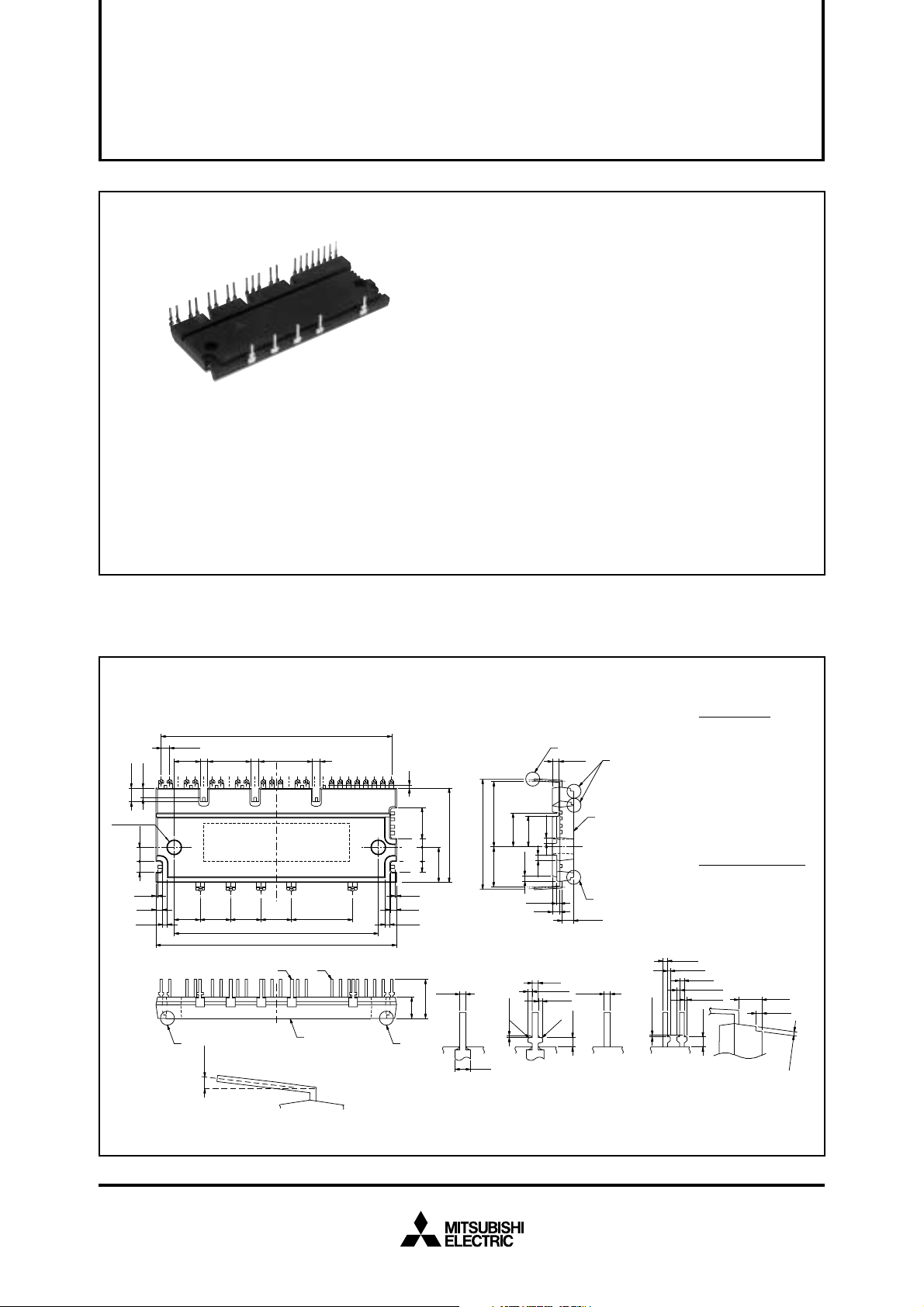
Fig. 1 PACKAGE OUTLINES
±0.3
2.8
(2.4) (2.5) (2.4)
(8.5)
(14.4) (17.6)
7305283
31
Type name , Lot No.
22 23 24 25
±0.3
±
0.3
10
10
(0 ~ 5°)
2-φ4.5
2468
1
(4.5)
(3.1)
27
±0.2
(4.65)
41
(3.5)
(0.6)
(2)
8.5
(1.5)
D D
(Short-pin type : PS21869-P) Refer Fig. 6 for long-pin type : PS21869-AP.
27×2.8(=75.6)
C
1333121110
9
35
343229
±0.3
±0.3
10
67
79
±0.3
20
±0.3
±0.5
BA
HEAT SINK SIDE
2120191817161514
(1)
36
37
38
39
(2.9) (10)
0.5
(4.65)
(0.6)
(2)
(3.5)
±
11.5
40
26
(1.5)
±0.2
1
±0.5
±0.5
12.8
7
±0.5
21.4
±0.5
±0.5
31
34.9
±0.5
13.4
(11)
(10)
(1.5)
1 MIN
C
0.2
0.5MAX
(1.5)
2.5
(1.5)
1
0.7
0.7
C0.2
±0.2
±0.2
±0.2
Irregular solder remains
(2.5)
TERMINAL 22, 26
OTHER TERMINAL
DETAIL A (5 pins t = 0.7) DETAIL B (21 pins t = 0.7) DETAIL D (5 parts)
(2.2)
D
HEAT SINK SIDE
D
±0.2
3.8
±0.2
0.8
±0.5
1.6
OTHER TERMINAL
TERMINAL CODE
1. UP
2. VP1
3. VUFB
4. VUFS
5. VP
6. VP1
7. VVFB
8. VVFS
9. WP
10. VP1
11. VPC
12. VWFB
13. VWFS
DUMMY TERMINAL CODE
27. VPC
28. UPG
29. P
30. VPC
31. VPG
32. U
33. WPG
34. V
±0.2
0.8
±0.2
0.45
±0.2
0.8
±0.2
0.45
±0.2
0.45
0.5MAX
±0.5
1.6
Irregular solder remains
TERMINAL 1-2, 20-21
Dimensions in mm
14. VN1
15. VNC
16. CIN
17. CFO
18. FO
19. UN
20. VN
21. WN
22. P
23. U
24. V
25. W
26. N
35. UNG
36. VNC
37. VNO
38. WNG
39. VNG
40. W
41. P
(3.8)
1MIN
0.7MIN
DETAIL C (2 parts)
All outer lead terminals are with Pb-free solder (Sn-Cu) plating.
Jul. 2005
MITSUBISHI SEMICONDUCTOR <Dual-In-Line Package Intelligent Power Module>
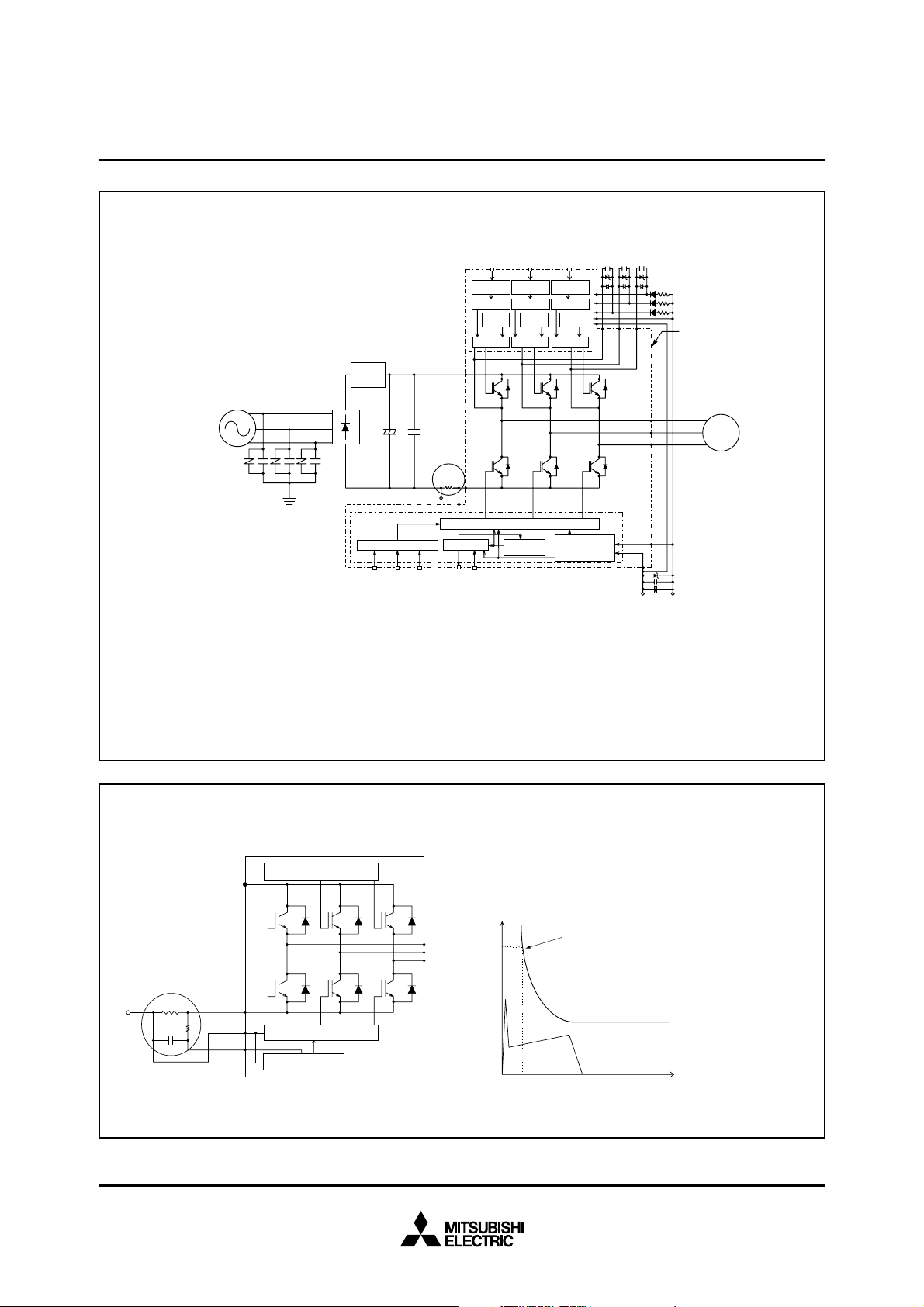
Fig. 2 INTERNAL FUNCTIONS BLOCK DIAGRAM (TYPICAL APPLICATION EXAMPLE)
CBV+
CBU–
CBV–
C1 : Tight tolerance, temp-compensated electrolytic type
(Note : The capacitance value depends on the PWM control
scheme used in the applied system).
C2 : 0.22~2µF R-category ceramic capacitor for noise filtering.
Inrush current
limiter circuit
High-side input (PWM)
(3, 5V line) (Note 1, 2)
Input signal
conditioning
Level shifter
Protection
circuit (UV)
Drive circuit
P
Input signal
Input signal
conditioning
conditioning
Level shifter Level shifter
Drive circuit Drive circuit
Protection
circuit (UV)
Protection
circuit (UV)
CBU+
PS21869-P/AP
TRANSFER-MOLD TYPE
INSULATED TYPE
CBW+
CBW–
C2
(Note 7)
C1
(Note 6)
DIP-IPM
AC line input
(Note 4)
C
Z
Z : ZNR (Surge absorber)
C : AC filter (Ceramic capacitor 2.2~6.5nF)
(Note : Additionally, an appropriate line-to line
surge absorber circuit may become necessary
depending on the application environment).
Note1: Input logic is high-active. There is a 2.5kΩ (min) pull-down resistor built-in each input circuit. When using an external CR filter, please make it satisfy the
input threshold voltage.
2: By virtue of integrating an application specific type HVIC inside the module, direct coupling to MCU terminals without any opto-coupler or transformer
isolation is possible. (see also Fig. 10)
3: This output is open drain type. The signal line should be pulled up to the positive side of the 5V power supply with approximately 10kΩ resistance.
(see also Fig. 10)
4: The wiring between the power DC link capacitor and the P, N1 terminals should be as short as possible to protect the DIP-IPM against catastrophic high
surge voltages. For extra precaution, a small film type snubber capacitor (0.1~0.22µF, high voltage type) is recommended to be mounted close to
these P-N1 DC power input pins.
5: Fo output pulse width should be decided by putting external capacitor between CFO and V
6: High voltage (600V or more) and fast recovery type (less than 100ns) diodes should be used in the bootstrap circuit.
7: It is recommended to insert a Zener diode (24V/1W) nearby each pair of supply terminals to prevent surge destruction.
Input signal conditioning
Low-side input (PWM)
(3, 5V line) (Note 1, 2)
Fig. 3
N1
VNC
Fo logic
FO CFO
Fault output (5V line)
(Note 3, 5)
N
CIN
Drive circuit
Fig. 3 EXTERNAL PART OF THE DIP-IPM PROTECTION CIRCUIT
DIP-IPM
P
H-side IGBT
External protection circuit
Shunt Resistor
N1
(Note 1)
R
C
C
Note1: In the recommended external protection circuit, please select the RC time constant in the range 1.5~2.0µs.
2: To prevent erroneous protection operation, the wiring of A, B, C should be as short as possible.
L-side IGBT
A
N
NC
V
CIN
B
(Note 2)
Drive circuit
S
S
Drive circuit
Protection circuit
Short Circuit Protective Function (SC) :
SC protection is achieved by sensing the L-side DC-Bus current (through the external
shunt resistor) after allowing a suitable filtering time (defined by the RC circuit).
When the sensed shunt voltage exceeds the SC trip-level, all the L-side IGBTs are turned
OFF and a fault signal (Fo) is output. Since the SC fault may be repetitive, it is
recommended to stop the system when the Fo signal is received and check the fault.
IC (A)
U
V
W
0
H-side IGBT
S
U
V
W
L-side IGBTS
Protection
circuit
Control supply
Under-Voltage
protection
VNC
(15V line)
NC terminals. (Example : CFO=22nF → tFO=1.8ms (Typ.))
SC Protection
Trip Level
Collector current
waveform
2
w
(µs)
t
AC line output
(Note 7)
D
V
M
Jul. 2005
MITSUBISHI SEMICONDUCTOR <Dual-In-Line Package Intelligent Power Module>
PS21869-P/AP
TRANSFER-MOLD TYPE
INSULATED TYPE
MAXIMUM RATINGS (Tj = 25°C, unless otherwise noted)
INVERTER PART
ConditionSymbol Parameter Ratings Unit
CC
V
VCC(surge)
VCES
±IC
±ICP
PC
Tj
Supply voltage
Supply voltage (surge)
Collector-emitter voltage
Each IGBT collector current
Each IGBT collector current (peak)
Collector dissipation
Junction temperature
Applied between P-N
Applied between P-N
T
f = 25°C
f = 25°C, less than 1ms
T
f = 25°C, per 1 chip
T
(Note 1)
450
500
600
50
100
70.4
–20~+125
Note 1 : The maximum junction temperature rating of the power chips integrated within the DIP-IPM is 150°C (@ Tf ≤ 100°C) however, to en-
sure safe operation of the DIP-IPM, the average junction temperature should be limited to Tj(ave) ≤ 125°C (@ Tf ≤ 100°C).
CONTROL (PROTECTION) PART
ConditionSymbol Parameter Ratings Unit
VD
VDB
VIN
VFO
IFO
VSC
Control supply voltage
Control supply voltage
Input voltage
Fault output supply voltage
Fault output current
Current sensing input voltage
Applied between V
Applied between VUFB-VUFS, VVFB-VVFS,
Applied between UP, VP, WP-VPC, UN, VN,
Applied between FO-VNC
Sink current at FO terminal
Applied between CIN-V
P1-VPC, VN1-VNC
VWFB-VWFS
WN-VNC
NC
–0.5~V
–0.5~V
–0.5~V
20
20
D+0.5
D+0.5
1
D+0.5
V
V
V
A
A
W
°C
V
V
V
V
mA
V
TOTAL SYSTEM
Symbol Ratings Unit
V
CC(PROT)
Tf
Tstg
Viso
Self protection supply voltage limit
(short circuit protection capability)
Module case operation temperature
Storage temperature
Isolation voltage
Parameter
D = 13.5~16.5V, Inverter part
V
Tj = 125°C, non-repetitive, less than 2 µs
60Hz, Sinusoidal, AC 1 minute, connection
pins to heat-sink plate
Note 2 : Tf measurement point
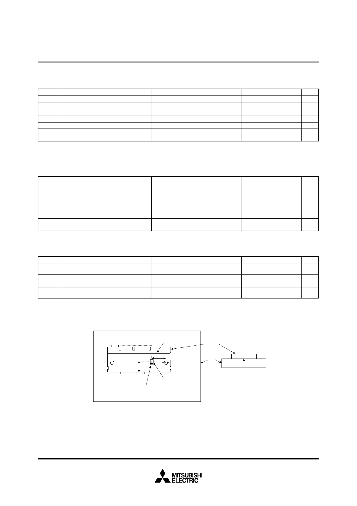
Al Board Specification :
Dimensions : 100✕100✕10mm, Finishing : 12s, Warp : –50~100µm
Silicon-grease should be applied evenly with a thickness of 100~200µm
Control Terminals
13.5mm
PUVW N
Power Terminals
FWDi Chip
Groove
18mm
IGBT Chip
Temp. measurement point
(inside the AI board)
Condition
DIP-IPM
AI board
(Note 2)
Temp. measurement point
(inside the AI board)
400
–20~+100
–40~+125
2500
V
°C
°C
rms
V
Jul. 2005
 Loading...