

MITSUBISHI PS21765 Technical data
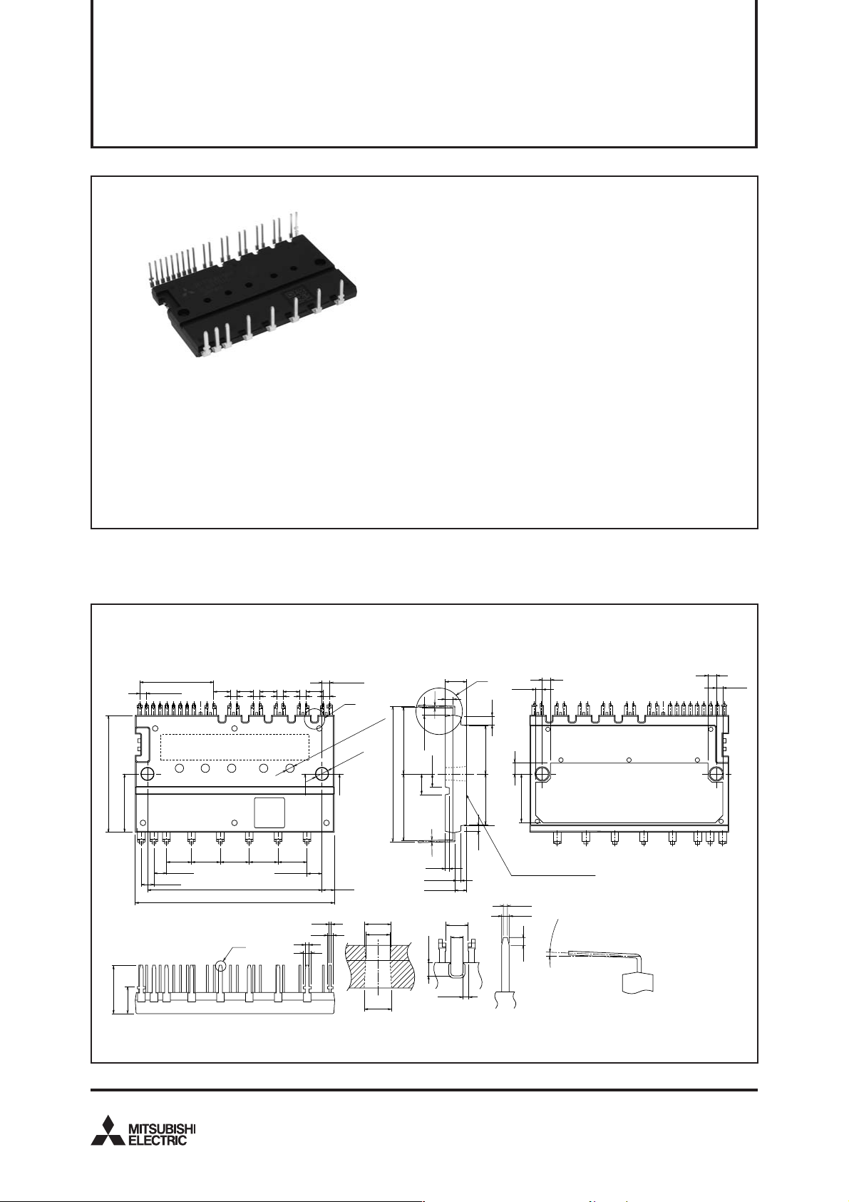
MITSUBISHI SEMICONDUCTOR <Dual-In-Line Package Intelligent Power Module>
MITSUBISHI SEMICONDUCTOR <Dual-In-Line Package Intelligent Power Module>
PS21765
TRANSFER-MOLD TYPE
TRANSFER-MOLD TYPE
INSULATED TYPE
INSULATED TYPE
PS21765
INTEGRATED DRIVE, PROTECTION AND SYSTEM CONTROL FUNCTIONS
• For upper-leg IGBTS : Drive circuit, High voltage high-speed level shifting, Control supply under-voltage (UV) protection.
• For lower-leg IGBT
• Fault signaling : Corresponding to an SC fault (Lower-leg IGBT) or a UV fault (Lower-side supply).
• Input interface : 3, 5V line (High Active)
•UL Approved : Yellow Card No. E80276
S : Drive circuit, Control supply under-voltage protection (UV), Short circuit protection (SC).
INTEGRATED POWER FUNCTIONS
600V/20A low-loss CSTBTTM inverter bridge with N-side
three-phase output DC-to-AC power conversion
PS21765
APPLICATION
AC100V~200V three-phase inverter drive for small power motor control.
Fig. 1 PACKAGE OUTLINES
±0.2
(11×1.78)
±0.2
1.78
28
27 26 25 24 23 22 21 2019 181716 151413 121110 987654321
29
30
31
15.5
32 33 34 35 36 37 38
31
6.6
3.3
±0.3
3.3
12.7
7.1
A = 1.78
±0.2
B = 4.32
BABABAB
B
A
Type name, Lot No.
QR
CODE
±0.3
±0.3
±0.3
46
52.5
±0.2
E
7.62
±0.3
±0.3
7.62
7.62
3.95
7.62
±0.3
±0.3
2
0.5
1.5
1
±0.3
2.04
A
D
5-φ2.2(DEPTH2.6)
2-φ3.3
CC
3.25
C-C
(φ3.5)
φ3.3
(φ3.7)
Note: All outer lead terminals are with lead free solder (Sn-Cu) plating.
2
0.5
17.7
(1.96)
(3.5)
±0.5
35.9
(5.5)
17.7
0.5
(1)
1.55
±0.1
3.1
(2.9)
(1.6)
(1.75)
(0.75)
DETAIL D DETAIL E
F
5.6
2.2
(12.78)(13.5)
1.5
(2.2)
(1.7)
(2.8)
(13)
HEAT SINK SIDE
(0.6)
(1)
°)
°~5
(0
(1)
Dimensions in mm
(2.2)
TERMINAL CODE
VUFS
1
2
3
4
5
6
7
8
9
10
11
12
13
14
15
16
17
18
19
(UPG)
VUFB
VP1
(COM)
UP
VVFS
(VPG)
VVFB
VP1
(COM)
VP
VWFS
(WPG)
VWFB
VP1
(COM)
WP
(UNG)
20
21
22
23
24
25
26
27
28
29
30
31
32
33
34
35
36
37
38
(1.7)
VNO
UN
VN
WN
FO
CFO
CIN
VNC
VN1
(WNG)
(VNG)
NW
NV
NU
W
V
U
P
NC
Aug. 2007
1
MITSUBISHI SEMICONDUCTOR <Dual-In-Line Package Intelligent Power Module>
MAXIMUM RATINGS (Tj = 25°C, unless otherwise noted)
INVERTER PART
CC
V
VCC(surge)
VCES
±IC
±ICP
PC
Tj
Supply voltage
Supply voltage (surge)
Collector-emitter voltage
Each IGBT collector current
Each IGBT collector current (peak)
Collector dissipation
Junction temperature
CONTROL (PROTECTION) PART
Parameter
D
V
VDB
VIN
VFO
IFO
VSC
Control supply voltage
Control supply voltage
Input voltage
Fault output supply voltage
Fault output current
Current sensing input voltage
Applied between P-NU, NV, NW
Applied between P-NU, NV, NW
T
T
T
Applied between V
Applied between VUFB-VUFS, VVFB-VVFS,
Applied between UP, VP, WP, UN, VN, WN-
Applied between FO-VNC
Sink current at FO terminal
Applied between CIN-V
ConditionSymbol Parameter Ratings Unit
c = 25°C
c = 25°C, less than 1ms
c = 25°C, per 1 chip
ConditionSymbol
P1-VNC, VN1-VNC
VWFB-VWFS
VNC
NC
PS21765
TRANSFER-MOLD TYPE
INSULATED TYPE
450
500
600
20
40
76.9
–20~+150
Ratings Unit
20
20
–0.5~V
D+0.5
D+0.5
–0.5~V
1
–0.5~V
D+0.5
V
V
V
A
A
W
°C
V
V
V
V
mA
V
TOTAL SYSTEM
Symbol Ratings Unit
V
CC(PROT)
Tc
Tstg
Viso
Note 1 : T
Self protection supply voltage limit
(short circuit protection capability)
Module case operation temperature
Storage temperature
Isolation voltage
C measurement point
Parameter
18mm
IGBT Chip position
FWDi Chip position
D = 13.5~16.5V, Inverter part
V
Tj = 125°C, non-repetitive, less than 2 µs
60Hz, Sinusoidal, AC 1 minute,
All pins to heat-sink plate
Control Terminals
18mm
Power Terminals
Condition
Groove
Tc point
(Note 1)
400
–20~+100
–40~+125
2500
DIP-IPM
Heat sink side
V
°C
°C
rms
V
Aug. 2007
2
MITSUBISHI SEMICONDUCTOR <Dual-In-Line Package Intelligent Power Module>
PS21765
TRANSFER-MOLD TYPE
INSULATED TYPE
THERMAL RESISTANCE
Parameter
Rth(j-c)Q
Rth(j-c)F
Note 2 : Grease with good thermal conductivity should be applied evenly with about +100µm~+200µm on the contacting surface of DIP-IPM
Junction to case thermal
resistance (Note 2)
and heat-sink.
The contacting thermal resistance between DIP-IPM case and heat sink (R
ductivity of the applied grease. For reference, R
thermal conductivity is 1.0W/m·k
Inverter IGBT part (per 1/6 module)
Inverter FWD part (per 1/6 module)
th(c-f) (per 1/6 module) is about 0.3°C/W when the grease thickness is 20µm and the
ConditionSymbol
th(c-f)) is determined by the thickness and the thermal con-
Min.
Limits
Typ. Max.
—
—
—
—
ELECTRICAL CHARACTERISTICS (Tj = 25°C, unless otherwise noted)
INVERTER PART
Symbol Parameter
V
CE(sat)
VEC
Collector-emitter saturation
voltage
FWDi forward voltage
ton
trr
tc(on)
Switching times
toff
tc(off)
ICES
Collector-emitter cut-off
current
Condition
VD = VDB = 15V
VIN = 5V
C = 20A, Tj = 25°C
I
IC = 20A, Tj = 125°C
Tj = 25°C, –IC = 20A, VIN = 0V
CC = 300V, VD = VDB = 15V
V
IC = 20A, Tj = 125°C, VIN = 0 ↔ 5V
Inductive load (upper-lower arm)
T
CE = VCES
V
j = 25°C
Tj = 125°C
Min. Typ. Max.
0.70
Limits
—
1.60
—
1.70
—
1.50
1.30
—
0.30
—
0.50
—
1.30
—
0.40
—
—
—
—
2.10
2.20
2.00
1.90
0.80
1.90
0.60
1.3
3.0
—
10
Unit
°C/W
°C/W
Unit
V
V
µs
µs
µs
µs
µs
1
mA
CONTROL (PROTECTION) PART
—
—
—
—
4.9
—
1.0
1.0
—
0.8
0.5
Limits
—
—
—
—
—
—
0.48
1.5
—
—
—
—
1.8
2.3
1.4
0.9
7.00
0.55
7.00
0.55
0.95
0.53
12.0
12.5
12.5
13.0
Symbol
I
D
VFOH
VFOL
VSC(ref)
IIN
UVDBt
UVDBr
UVDt
UVDr
tFO
Vth(on)
Vth(off)
Vth(hys)
Parameter Condition
VD = VDB = 15V
V
Circuit current
Fault output voltage
Short circuit trip level
Input current
Control supply under-voltage
protection
Fault output pulse width
IN = 5V
V
D = VDB = 15V
V
IN = 0V
VSC = 0V, FO terminal pull-up to 5V with 10kΩ
V
SC = 1V, IFO = 1mA
T
j = 25°C, VD = 15V (Note 3)
V
IN = 5V
Tj ≤ 125°C
C
FO = 22nF (Note 4)
ON threshold voltage
OFF threshold voltage
Applied between U
ON/OFF threshold hysteresis voltage
Total of V
P1-VNC, VN1-VNC
VUFB-VUFS, VVFB-VVFS, VWFB-VWFS
Total of V
P1-VNC, VN1-VNC
VUFB-VUFS, VVFB-VVFS, VWFB-VWFS
Trip level
Reset level
Trip level
Reset level
P, VP, WP, UN, VN, WN-VNC
Min. Typ. Max.
0.43
10.0
10.5
10.3
10.8
Note 3 : Short circuit protection is functioning only at the low-arms. Please select the external shunt resistance such that the SC trip-level is
less than 2.0 times of the current rating.
4:Fault signal is output when the low-arms short circuit or control supply under-voltage protective functions works. The fault output pulse-
width tFO depends on the capacitance of CFO according to the following approximate equation : CFO = 12.2 ✕ 10-6 ✕ tFO [F].
—
2.0
—
2.6
—
—
Unit
mA
mA
mA
mA
V
V
V
mA
V
V
V
V
ms
V
V
V
Aug. 2007
3
 Loading...