

MITSUBISHI PS21562-SP Technical data
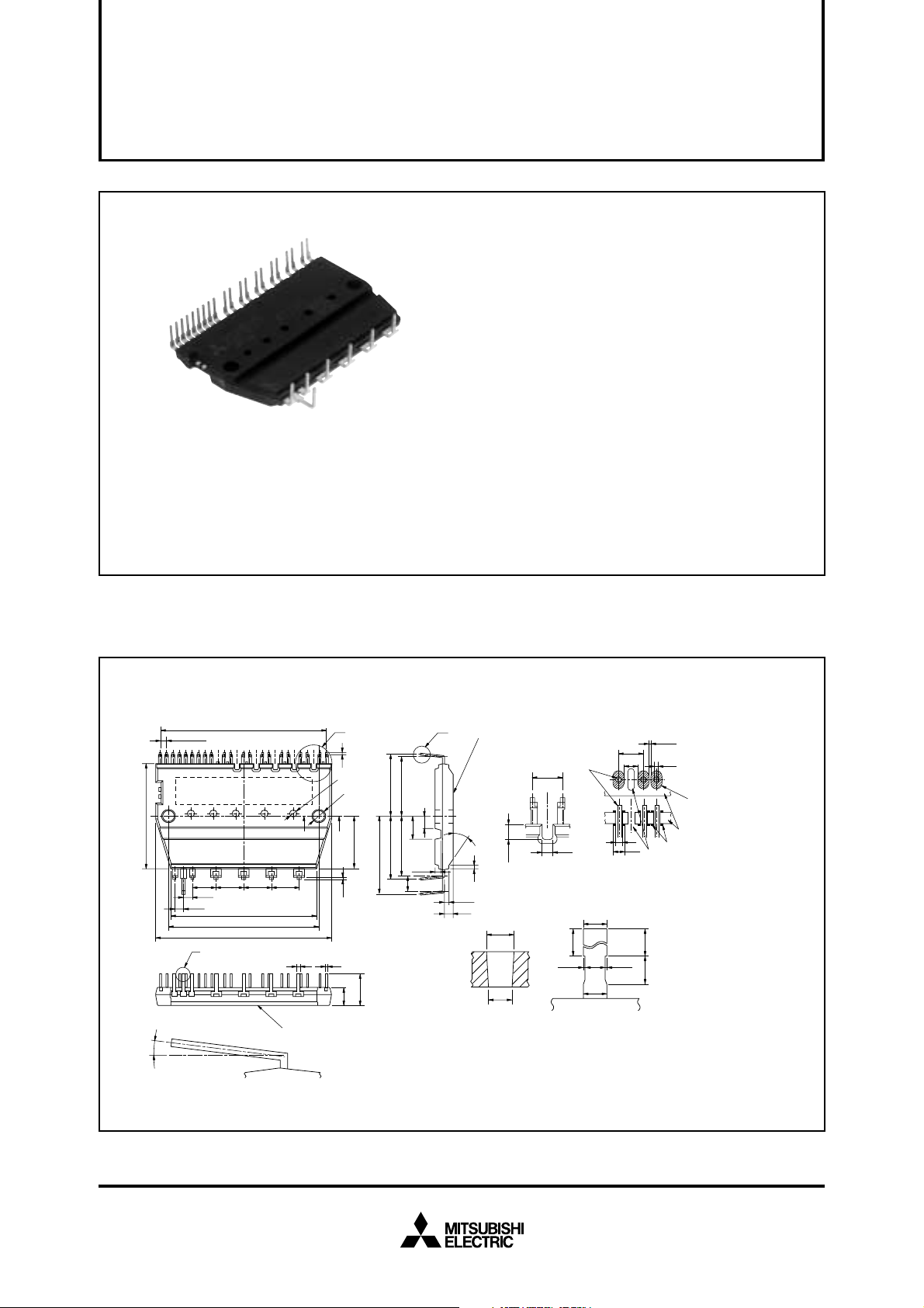
MITSUBISHI SEMICONDUCTOR <Dual-In-Line Package Intelligent Power Module>
MITSUBISHI SEMICONDUCTOR <Dual-In-Line Package Intelligent Power Module>
PS21562-SP
TRANSFER-MOLD TYPE
INSULATED TYPE
INSULA TED TYPE
PS21562-SP
PS21562-SP
TRANSFER-MOLD TYPE
INTEGRATED POWER FUNCTIONS
600V/5A low-loss 5th generation IGBT inverter bridge for
three phase DC-to-AC power conversion.
Open emitter type.
INTEGRATED DRIVE, PROTECTION AND SYSTEM CONTROL FUNCTIONS
• For upper-leg IGBTS :Drive circuit, High voltage isolated high-speed level shifting, Control supply under-voltage (UV) protection.
• For lower-leg IGBT
• Fault signaling : Corresponding to an SC fault (Lower-leg IGBT) or a UV fault (Lower-side supply).
• Input interface : 3,5V line CMOS/TTL compatible. (High Active)
• UL Approved : Yellow Card No. E80276
S : Drive circuit, Control supply under-voltage protection (UV), Short circuit protection (SC).
APPLICATION
AC100V~200V inverter drive for small power motor control.
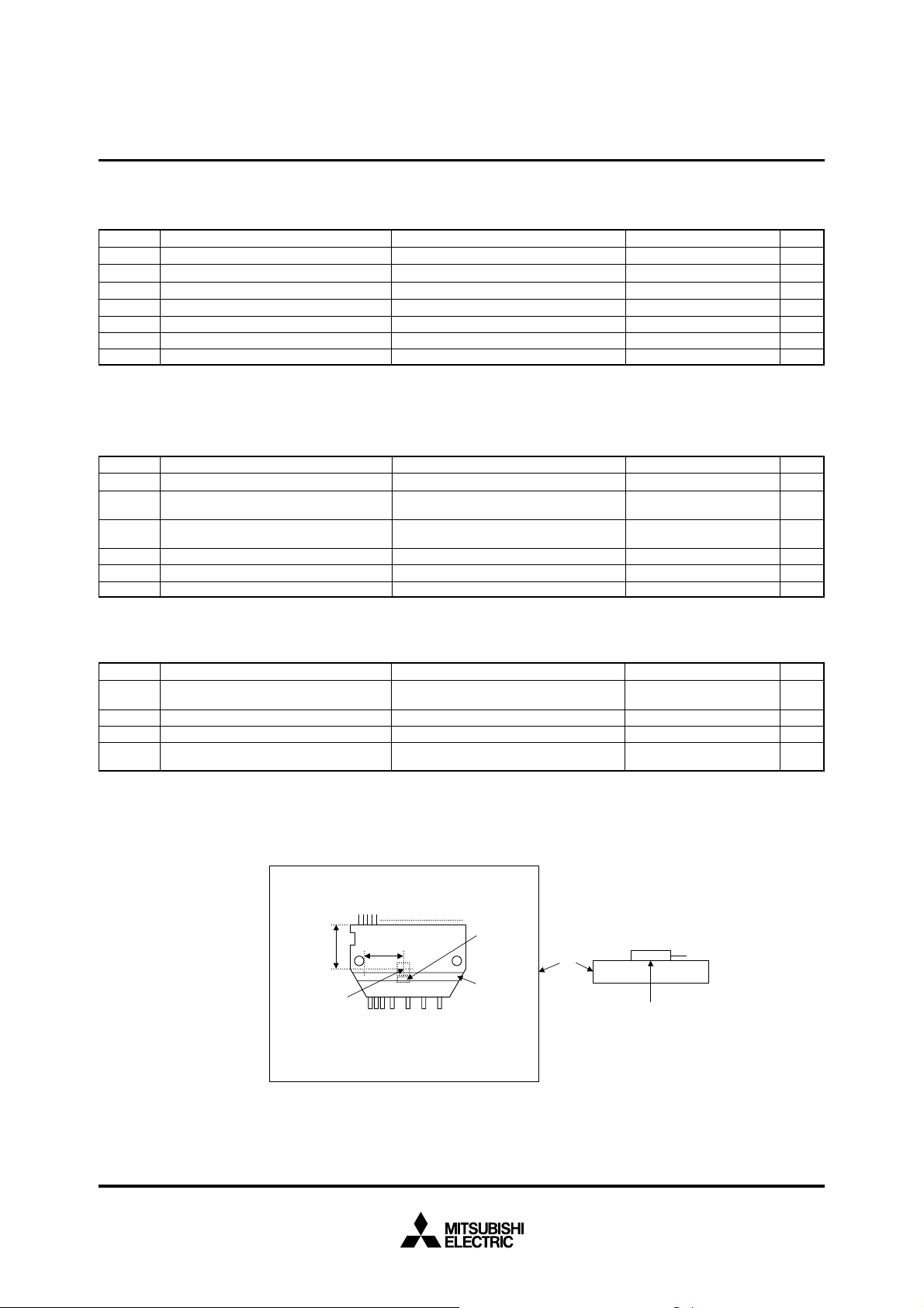
Fig. 1 PACKAGE OUTLINES
±0.15
1.778
26 252728
29
Type name , Lot No.
30
30.5
35 3437 36 33 32 31
2.54
C
°)
(0~5
1.778 × 26 (=46.228)
161718 131415 10 987 654 321
7.62
(41)
±0.15
42
49
7.62 7.62
6.7
2.54
12192021222324
11
DETAIL D
HEAT SINK SIDE
0.8 0.5
A
0.5
(φ2 DEPTH 2)
φ3.3
BB
15.25
0.5
9
5
D
HEAT SINK SIDE
3.556
(17.6)
35°
(3.5)
(6.5)
17.4 17.4
(22.1)
(17.6)
(1.5)
4.5
1.25
1.75
1.2
2.5
(φ3.8)
NO SOLDER PLATING
(0.05) (0.05)
φ3.3
B-B
All outer lead terminals are with Pb-free solder plating.
TERMINAL
1.2
DETAIL A
0.8
ON BOTH LEAD SIDE
(0.7)
0.8
DETAIL C
(36 TERMINAL)
(0.278)
3.556
(2.056)
(0.5)
(1)
(1.5)
SLIT
(ex. PCB LAYOUT)
(1.5)(1)
(R
0.7
5)
PCB
PATTERN
Note1)
Dimensions in mm
TERMINAL CODE
1 VUFS
2 (UPG)
3 VUFB
4 VP1
5 (COM)
6 UP
7 VVFS
8 (VPG)
9 VVFB
10 VP1
11 (COM)
12 VP
13 VWFS
14 (WPG)
15 VWFB
16 VP1
17 (COM)
18 WP
19 (UNG)
20 VNO
21 UN
22 VN
23 WN
24 FO
25 CFO
26 CIN
27 VNC
28 VN1
29 (WNG)
30 (VNG)
31 P
32 U
33 V
34 W
35 NU
36 NV
37 NW
Note 1: In order to get enough creepage distance between the terminals, please take some countermeasure such as a slit on PCB.
Jul. 2005
MITSUBISHI SEMICONDUCTOR <Dual-In-Line Package Intelligent Power Module>
PS21562-SP
TRANSFER-MOLD TYPE
INSULATED TYPE
MAXIMUM RATINGS (Tj = 25°C, unless otherwise noted)
INVERTER PART
ConditionSymbol Parameter Ratings Unit
CC
V
VCC(surge)
VCES
±IC
±ICP
PC
Tj
Supply voltage
Supply voltage (surge)
Collector-emitter voltage
Each IGBT collector current
Each IGBT collector current (peak)
Collector dissipation
Junction temperature
Applied between P-NU, NV, NW
Applied between P-NU, NV, NW
T
f = 25°C
f = 25°C, less than 1ms
T
f = 25°C, per 1 chip
T
(Note 1)
450
500
600
5
10
16.7
–20~+125
Note 1 : The maximum junction temperature rating of the power chips integrated within the DIP-IPM is 150°C (@ Tf ≤ 100°C) however, to en-
sure safe operation of the DIP-IPM, the average junction temperature should be limited to Tj(ave) ≤ 125°C (@ Tf ≤ 100°C).
CONTROL (PROTECTION) PART
ConditionSymbol Parameter Ratings Unit
VD
VDB
VIN
VFO
IFO
VSC
Control supply voltage
Control supply voltage
Input voltage
Fault output supply voltage
Fault output current
Current sensing input voltage
Applied between V
Applied between VUFB-VUFS, VVFB-VVFS,
Applied between UP, VP, WP, UN, VN,
Applied between FO-VNC
Sink current at FO terminal
Applied between CIN-V
P1-VNC, VN1-VNC
VWFB-VWFS
WN-VNC
NC
–0.5~V
–0.5~V
–0.5~V
20
20
D+0.5
D+0.5
1
D+0.5
V
V
V
A
A
W
°C
V
V
V
V
mA
V
TOTAL SYSTEM
Symbol Ratings Unit
V
CC(PROT)
Tf
Tstg
Viso
Self protection supply voltage limit
(short circuit protection capability)
Module case operation temperature
Storage temperature
Isolation voltage
Parameter
D = 13.5~16.5V, Inverter part
V
Tj = 125°C, non-repetitive, less than 2 µs
60Hz, Sinusoidal, 1 minute,
All connected pins to heat-sink plate
Note 2 : Tf measurement point
Al Board Specification :
Dimensions : 100✕100✕10mm, Finishing : 12s, Warp : –50~100µm
Control Terminals
18mm
IGBT Chip
Temperature
measurement point
(inside the AI board)
Silicon-grease should be applied evenly with a thickness of 100~200µm
16mm
PUVWN
Power Terminals
Condition
FWDi Chip
Groove
Al Board
(Note 2)
DIP-IPM
Temperature measurement
point (inside the AI board)
400
–20~+100
–40~+125
2500
V
°C
°C
rms
V
Jul. 2005
MITSUBISHI SEMICONDUCTOR <Dual-In-Line Package Intelligent Power Module>
PS21562-SP
TRANSFER-MOLD TYPE
INSULATED TYPE
THERMAL RESISTANCE
Parameter
Rth(j-f)Q
Rth(j-f)F
Note 3: Grease with good thermal conductivity should be applied evenly with about +100µm~+200µm on the contacting surface of DIP-IPM
Junction to case thermal
resistance (Note 3)
and heat-sink.
Inverter IGBT part (per 1/6 module)
Inverter FWD part (per 1/6 module)
ConditionSymbol
Min.
Limits
Typ. Max.
—
—
—
—
ELECTRICAL CHARACTERISTICS (Tj = 25°C, unless otherwise noted)
INVERTER PART
Symbol
V
CE(sat)
VEC
ton
trr
tc(on)
toff
tc(off)
ICES
Parameter
Collector-emitter saturation
voltage
FWD forward voltage
Switching times
Collector-emitter cut-off
current
Condition
VD = VDB = 15V
VIN = 5V
C = 5A, Tj = 25°C
I
IC = 5A, Tj = 125°C
Tj = 25°C, –IC = 5A, VIN = 0V
CC = 300V, VD = VDB = 15V
V
IC = 5A, Tj = 125°C, VIN = 0
↔
Inductive load (upper-lower arm)
T
CE = VCES
V
j = 25°C
Tj = 125°C
Min. Typ. Max.
0.60
5V
Limits
—
1.60
—
1.70
—
1.50
1.20
—
0.30
—
0.40
—
1.30
—
0.50
—
—
—
—
2.10
2.20
2.00
1.80
0.60
2.00
0.80
6.0
6.5
—
10
Unit
°C/W
°C/W
Unit
V
V
µs
µs
µs
µs
µs
1
mA
CONTROL (PROTECTION) PART
—
—
—
—
4.9
—
1.0
1.0
2.1
0.8
Limits
—
—
—
—
—
—
—
1.5
—
—
—
—
1.8
2.3
1.4
5.00
0.40
7.00
0.55
0.95
0.52
12.0
12.5
12.5
13.0
Symbol
I
D
VFOH
VFOL
VSC(ref)
IIN
UVDBt
UVDBr
UVDt
UVDr
tFO
Vth(on)
Vth(off)
Parameter Condition
Circuit current
Fault output voltage
Short circuit trip level
Input current
Control supply under-voltage
protection
Fault output pulse width
ON threshold voltage
OFF threshold voltage
D = VDB = 15V
V
V
IN = 5V
V
D = VDB = 15V
V
IN = 0V
Total of V
P1-VNC, VN1-VNC
VUFB-VUFS, VVFB-VVFS, VWFB-VWFS
Total of V
P1-VNC, VN1-VNC
VUFB-VUFS, VVFB-VVFS, VWFB-VWFS
VSC = 0V, FO circuit pull-up to 5V with 10kΩ
V
SC = 1V, IFO = 1mA
T
f = –20~100°C, VD = 15V (Note 4)
V
IN = 5V
Trip level
Tj ≤ 125°C
Reset level
Trip level
Reset level
C
FO = 22nF (Note 5)
Applied between U
P, VP, WP-VNC, UN, VN, WN-VNC
Min. Typ. Max.
0.45
10.0
10.5
10.3
10.8
Note 4: Short circuit protection is functioning only for the lower-arms. Please select the external shunt resistance such that the SC trip-level is
less than 2.0 times of the current rating.
5:Fault signal is asserted corresponding to a short circuit or lower side control supply under-voltage failure. The fault output pulse width tFO
depends on the capacitance value of CFO according to the following approximate equation : CFO = 12.2 ✕ 10-6 ✕ tFO [F].
—
2.0
—
2.6
2.1
Unit
mA
V
V
V
mA
V
V
V
V
ms
V
V
Jul. 2005
 Loading...