

Mitsubishi PS21313 Datasheet
MITSUBISHI SEMICONDUCTOR <Dual-In-Line Package Intelligent Power Module>
MITSUBISHI SEMICONDUCTOR <Dual-In-Line Package Intelligent Power Module>
PS21313
INSULA TED TYPE
PS21313
PS21313
TRANSFER-MOLD TYPE
TRANSFER-MOLD TYPE
INSULA TED TYPE
INTEGRATED POWER FUNCTIONS
3rd generation IGBT inverter bridge for 3 phase DC-to-AC
power conversion.
INTEGRATED DRIVE, PROTECTION AND SYSTEM CONTROL FUNCTIONS
• For upper-leg IGBTS :Drive circuit, High voltage isolated high-speed level shifting, Control circuit under-voltage (UV) protection.
Note : Bootstrap supply scheme can be applied.
• For lower-leg IGBT
• Fault signaling : Corresponding to a SC fault (Low-side IGBT) or a UV fault (Low-side IGBT).
• Input interface : 5V line CMOS/TTL compatible, Schmitt Trigger receiver circuit.
S : Drive circuit, Control circuit under-voltage protection (UV), Short-circuit protection (SC).
APPLICATION
AC200V three-phase inverter drive for small power motor control.
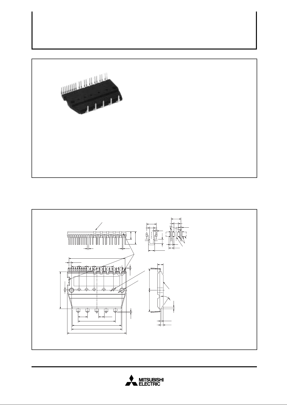
Fig. 1 PACKAGE OUTLINES
(1.778)
(6.25)(6.25)
(6.25)
26 252728
29
Type name , Lot No.
30
(0.75)
(30.5)
35 34 33 32 31
(7.62)
*Note 2: In order to increase the surface distance between terminals, cut a slit, etc. on the PCB surface
when mounting a module.
HEAT SINK SIDE
(1.778 × 26)
(8) (8)
161718 131415 10 987 654 321
12192021222324
11
(4MIN)
(7.62 × 4)
(41)
(42)
(49)
(3.556)
(1)
(6.5)
(10.5)
(0.5)(1)
DUMMY PIN
A
(0.5)
2 DEPTH 2)
φ
(
3.3)
φ
(
(0.5)
(1.8MIN)
(17.4)(17.4)
TERMINAL
(0.5)
(1.5)
Detail A
(5)
(35
(1.25)
(2.5)
(3.556)
(1.656)
(0.5)
(1)
(1.9)
SLIT
(PCB LAYOUT)
HEAT SINK SIDE
°
)
(1.2)
PCB
PATTERN
*Note2
TERMINAL CODE
1 VUFS
2 (UPG)
3 VUFB
4 VP1
5 (COM)
6 UP
7 VVFS
8 (VPG)
9 VVFB
10 VP1
11 (COM)
12 VP
13 VWFS
14 (WPG)
15 VWFB
16 VP1
17 (COM)
18 WP
19 (UNG)
20 VNO(NC)
21 UN
22 VN
23 WN
24 FO
25 CFO
26 CIN
27 VNC
28 VN1
29 (WNG)
30 (VNG)
31 P
32 U
33 V
34 W
35 N
*Note1:(***) = Dummy Pin.
* Note: The values used in the above figure are tentative.
Aug. 1999
MITSUBISHI SEMICONDUCTOR <Dual-In-Line Package Intelligent Power Module>
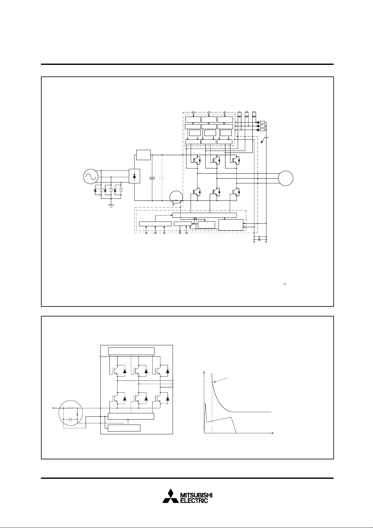
Fig. 2 INTERNAL FUNCTIONS BLOCK DIAGRAM (TYPICAL APPLICATION EXAMPLE)
CBW+
CBW–
CBV+
CBU–
CBV–
C3 : Tight tolerance, temp-compensated electrolytic type
(Note : The capacitance value depends on the PWM control
scheme used in the applied system).
C4 : 0.22~2µF R-category ceramic capacitor for noise filtering.
Inrush current
limiter circuit
High-side input (PWM)
(5V line) Note 1,2)
Input signal
coditioning
Level shifter
Protection
circuit (UV)
Drive circuit
P
Input signal
Input signal
coditioning
coditioning
Level shifter Level shifter
Protection
Protection
circuit (UV)
circuit (UV)
Drive circuit Drive circuit
CBU+
PS21313
TRANSFER-MOLD TYPE
INSULA TED TYPE
Bootstrap circuit
For detailed description
of the boot-strap circuit
C4
construction, please
C3
contact Mitsubishi
Electric
(Note 6)
DIP-IPM
AC input
(Note 4)
C
Z
Z : Surge absorber
C : AC filter (Ceramic capacitor 2.2~6.5nF)
(Protection against common-mode noise)
Note1: To prevent the input signals oscillation, an RC coupling at each input is recommended. (see also Fig. 6)
2: By virtue of integrating an application specific type HVIC inside the module, direct coupling to CPU terminals without any opto-coupler or transformer
isolation is possible. (see also Fig. 6)
3: This output is open collector type. The signal line should be pulled up to the positive side of the 5V power supply with approximately 5.1kΩ resistance.
(see also Fig. 6)
4: The wiring between the power DC link capacitor and the P/N1 terminals should be as short as possible to protect the DIP-IPM against catastrophic high
surge voltages. For extra precaution, a small film type snubber capacitor (0.1~0.22µF, high voltage type) is recommended to be mounted close to
these P and N1 DC power input terminals.
5: Fo output pulse width should be decided by connecting external capacitor between CFO and V
6: High voltage diodes (600V or more) should be used in the bootstrap circuit.
Input signal conditioning
Low-side input (PWM)
(5V line) (Note 1, 2)
Fig. 3
N
1
V
NC
Fo logic
FOCFO
FO output (5V line)
(Note 3, 5)
N
CIN
Drive circuit
SC
protection
H-side IGBT
S
U
V
W
L-side IGBT
Control supply
Under-Voltage
protection
NC terminals. (Example : CFO=22nF tFO=1.8ms (Typ.))
S
V
NC
(15V line)
V
Fig. 3 EXTERNAL PART OF THE DIP-IPM PROTECTION CIRCUIT
DIP-IPM
P
H-side IGBTS
External protection circuit
Shunt Resistor
N1
R
C
L-side IGBTS
A
N
NC
V
CIN
B
C
Note1: In the recommended external protection circuit, please select the RC time constant in the range 1.5~2.0µs.
2: To prevent erroneous protection operation, the wiring of A, B, C should be as short as possible.
Drive circuit
Drive circuit
Protection circuit
Short Circuit Protective Function (SC) :
SC protection is achieved by sensing the L-side DC-Bus current (through the external
shunt resistor) after allowing a suitable filtering time (defined by the RC circuit).
When the sensed shunt voltage exceeds the SC trip-level, all the L-side IGBTs are turned
OFF and a fault signal (Fo) is output. Since the SC fault may be repetitive, it is
recommended to stop the system when the Fo signal is received and check the fault.
IC (A)
SC Protection
waveform
Trip Level
w
(µs)
t
U
V
W
Collector current
0
2
M
AC line output
D
Aug. 1999
MITSUBISHI SEMICONDUCTOR <Dual-In-Line Package Intelligent Power Module>
PS21313
TRANSFER-MOLD TYPE
INSULA TED TYPE
MAXIMUM RATINGS (Tj = 25°C, unless otherwise noted)
INVERTER PART
ConditionSymbol Parameter Ratings Unit
CC
V
VCC(surge)
VCES
±IC
±ICP
PC
Tj
Supply voltage
Supply voltage (surge)
Collector-emitter voltage
Each IGBT collector current
Each IGBT collector current (peak)
Collector dissipation
Junction temperature
Applied between P-N
Applied between P-N
C = 25°C
T
C = 25°C, instantaneous value (pulse)
T
C = 25°C, per 1 chip
T
(Note 1)
450
500
600
10
20
25
–20~+150
Note 1 : The maximum junction temperature rating of the power chips integrated within the DIP-IPM is 150°C (@ Tf ≤ 100°C). However, to en-
sure safe operation of the DIP-IPM, the average junction temperature should be limited to T
j(ave) ≤ 125°C (@ Tf ≤ 100°C).
CONTROL (PROTECTION) PART
ConditionSymbol Parameter Ratings Unit
D
V
VDB
VCIN
VFO
IFO
VSC
Control supply voltage
Control supply voltage
Input voltage
Fault output supply voltage
Fault output current
Current sensing input voltage
Applied between V
Applied between VUFB-VUFS, VVFB -VVFS,
Applied between UP, VP, WP-VNC, UN, VN,
Applied between FO-VNC
Sink current at FO terminal
Applied between CIN-V
P1-VNC, VN1-VNC
V
WFB-VWFS
W
N-VNC
NC
20
20
–0.5~+5.5
–0.5~V
15
–0.5~V
D+0.5
D+0.5
V
V
V
A
A
W
°C
V
V
V
V
mA
V
TOTAL SYSTEM
Symbol Ratings Unit
CC(PROT)
V
Self protection supply voltage limit
(short-circuit protection capability)
Tf
Tstg
Viso
Heat-fin operation temperature
Storage temperature
Isolation voltage
Parameter Condition
D = 13.5~16.5V, Inverter part
V
T
j = 125°C, non-repetitive, less than 2 µs
(Note 2)
60Hz, Sinusoidal, AC 1 minute, connection
pins to heat-sink plate
400
–20~+100
–40~+125
1500
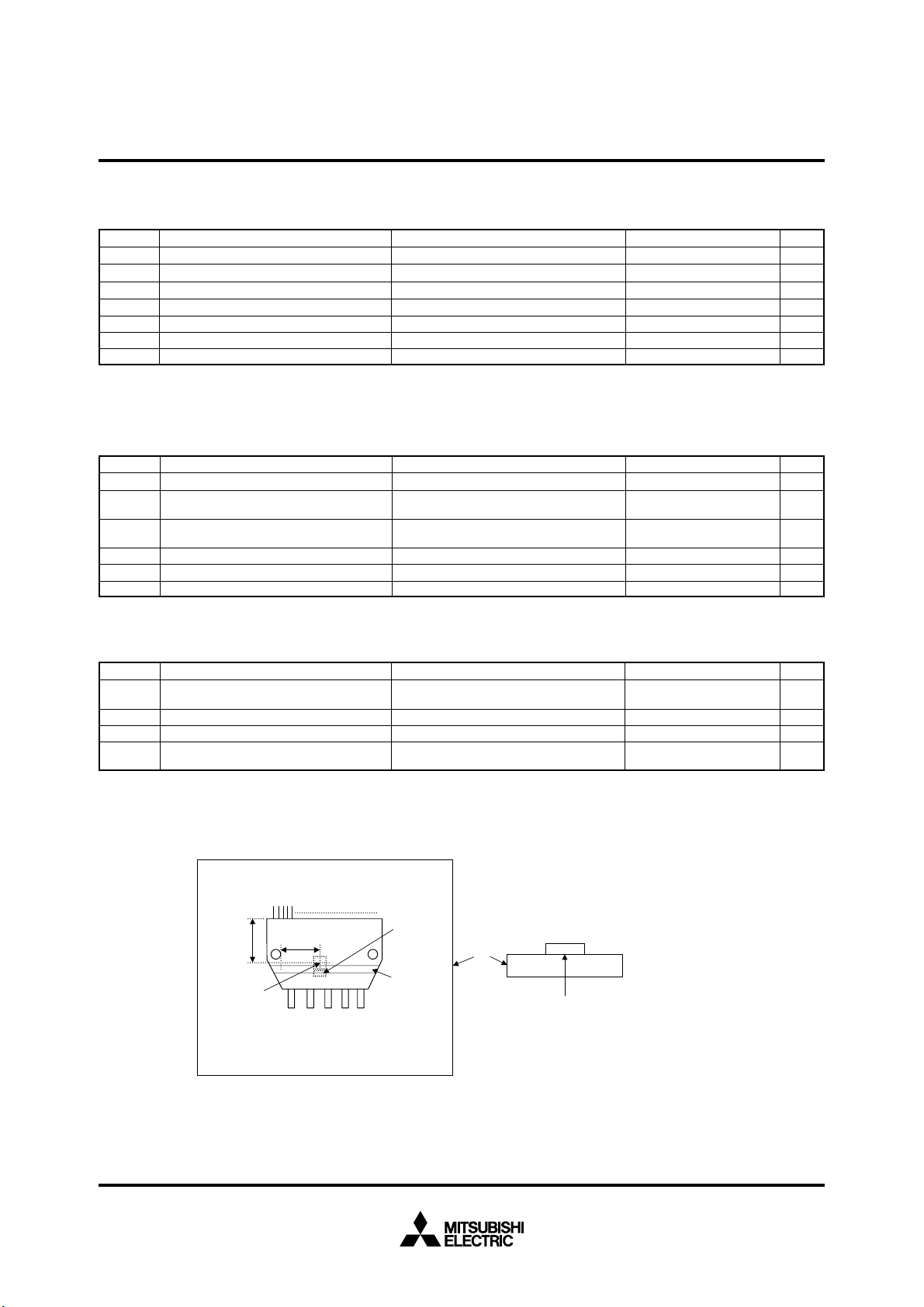
Note 2 : Tf MEASUREMENT POINT
Al Board Specifications:
Dimensions 100 × 100 × 10mm, finishing: 12s, warp: –50~100µm
C
Control Terminals
18mm
IGBT Chip
Temp. measurement
point
(inside the Al board)
100~200µm of evenly applied Silicon-Grease
16mm
Power Terminals
FWDi Chip
Al Board
Groove
PUVWN
IGBT/FWDi Chip
Temp. measurement point
(inside the Al board)
V
°C
°C
rms
V
Aug. 1999
 Loading...