

MITSUBISHI PM100CLA060 Technical data
查询PM100CLA060供应商
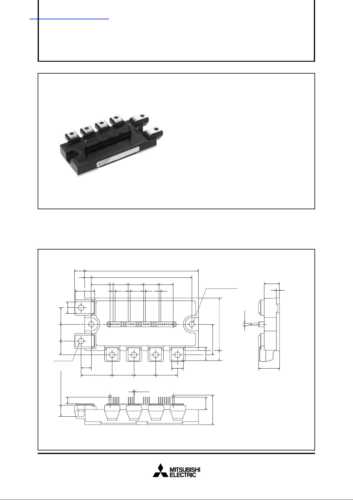
PM100CLA060
MITSUBISHI <INTELLIGENT POWER MODULES>
PM100CLA060
FLAT-BASE TYPE
INSULATED PACKAGE
FEATURE
a) Adopting new 5th generation IGBT (CSTBT) chip, which
performance is improved by 1µm fine rule process.
For example, typical V
b) I adopt the over-temperature conservation by Tj detection of
CSTBT chip, and error output is possible from all each conservation upper and lower arm of IPM.
c) New small package
Reduce the package size by 10%, thickness by 22% from
S-DASH series.
•3φ 100A, 600V Current-sense IGBT type inverter
• Monolithic gate drive & protection logic
• Detection, protection & status indication circuits for, shortcircuit, over-temperature & under-voltage (P-Fo available
from upper arm devices)
• Acoustic noise-less 11kW class inverter application
ce(sat)=1.5V @Tj=125°C
APPLICATION
General purpose inverter, servo drives and other motor controls
PACKAGE OUTLINES Dimensions in mm
12011
106
1616
16 15.25
6-23-23-23-2
UVW
12 22
19-■0.5
2-φ5.5
MOUNTING HOLES
5511.75
32
13.5
13
31
2-φ2.5
Terminal code
1. VUPC
2. UFO
3. UP
4. VUP1
5. VVPC
6. VFO
7. VP
8. VVP1
9. VWPC
10. WFO
16
+
1
–
0.5
11. WP
12. VWP1
13. VNC
14. VN1
15. NC
16. UN
17. VN
18. WN
19. Fo
3
12
17.5 17.5
14.5
6-M5 NUTS
7
(SCREWING DEPTH)
12
7
19.75
NP
10.75
3.25
19.75
1591319
B
32.75 23 23 23
Apr. 2004
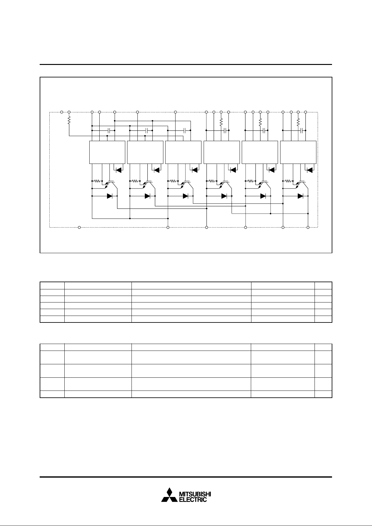
INTERNAL FUNCTIONS BLOCK DIAGRAM
V
NC
Fo V
NC
V
N1
W
N
N
MITSUBISHI <INTELLIGENT POWER MODULES>
PM100CLA060
FLAT-BASE TYPE
INSULATED PACKAGE
WPV
U
N
V
WPC
WF
WP1
O
V
VPC
VPV
VF
VP1
O
V
UPC
UPV
UF
UP1
O
Gnd In Fo Vcc
Gnd Si Out OT
NC N W V U P
Gnd In Fo Vcc
Gnd Si Out OT
Gnd In Fo Vcc
Gnd Si Out OT
Gnd In Fo Vcc
Gnd Si Out OT
Gnd In Fo Vcc
Gnd Si Out OT
Gnd In Fo Vcc
Gnd Si Out OT
MAXIMUM RATINGS (Tj = 25°C, unless otherwise noted)
INVERTER PART
Symbol Parameter Condition Ratings Unit
VCES
±IC
±ICP
PC
Tj
Collector-Emitter Voltage
Collector Current
Collector Current (Peak)
Collector Dissipation
Junction T emperature
V
D = 15V, VCIN = 15V
T
C = 25°C
T
C = 25°C
T
C = 25°C (Note-1)
600
100
200
356
–20 ~ +150
V
A
A
W
°C
CONTROL PART
Symbol Parameter Condition Ratings Unit
VD
VCIN
VFO
IFO
Supply Voltage
Input Voltage
Fault Output Supply Voltage
Fault Output Current
Applied between : V
Applied between : UP-VUPC, VP-VVPC
Applied between : UFO-VUPC, VFO-VVPC, WFO-VWPC
Sink current at UFO, VFO, WFO, FO terminals
UP1-VUPC
VVP1-VVPC, VWP1-VWPC, VN1-VNC
WP-VWPC, UN • VN • WN-VNC
FO-VNC
20
20
20
20
Apr. 2004
V
V
V
mA
TOTAL SYSTEM
Symbol
V
CC(PROT)
V
CC(surge)
TC
Tstg
Viso
Supply Voltage Protected by
SC
Supply Voltage (Surge)
Module Case Operating
Temperature
Storage Temperature
Isolation Voltage
(Note-1) Tc (base plate) measurement point is below.
Parameter
V
D = 13.5 ~ 16.5V, Inverter Part,
j = +125°C Start
T
Applied between : P-N, Surge value
(Note-1)
60Hz, Sinusoidal, Charged part to Base, AC 1 min.
Top view
Condition
UVW
MITSUBISHI <INTELLIGENT POWER MODULES>
PM100CLA060
FLAT-BASE TYPE
INSULATED PACKAGE
Ratings
400
500
–20 ~ +100
–40 ~ +125
2500
B
NP
Unit
V
°C
°C
V
rms
V
THERMAL RESISTANCES
Tc
Symbol
Rth(j-c)Q
Rth(j-c)F
Rth(j-c)Q
Rth(j-c)F
Rth(c-f)
Junction to case Thermal
Resistances
Contact Thermal Resistance
Parameter
Inverter IGBT part (per 1/6) (Note-2)
Inverter FWDi part (per 1/6) (Note-2)
Inverter IGBT part (per 1/6) (Note-1)
Inverter FWDi part (per 1/6) (Note-1)
Case to fin, (per 1 module)
Thermal grease applied (Note-1)
* If you use this value, Rth(f-a) should be measured just under the chips.
(Note-2) Tc (under the chip) measurement point is below.
axis
arm
X
Y
IGBT
28.3
–8.5
UP
FWDi
28.0
1.7
VP WP UN VN WN
FWDi
IGBT
FWDi
IGBT
87.2
87.0
65.2
65.0
1.7
–8.5
1.7
–8.5
Condition
IGBT
39.3
6.5
FWDi
39.5
–5.2
Bottom view
ELECTRICAL CHARACTERISTICS (Tj = 25°C, unless otherwise noted)
INVERTER PART
= 15V
Condition
(Fig. 5)
Symbol
CE(sat)
V
VEC
ton
trr
tc(on)
toff
tc(off)
ICES
Parameter
Collector-Emitter
Saturation Voltage
FWDi Forward Voltage
Switching Time
Collector-Emitter
Cutoff Current
D = 15V, IC = 100A
V
V
CIN = 0V, Pulsed (Fig. 1)
–I
C = 100A, VD = 15V, VCIN = 15V (Fig. 2)
D = 15V, VCIN = 0V↔15V
V
V
CC = 300V, IC = 100A
T
j = 125°C
Inductive Load (Fig. 3,4)
VCE = V
CES
, V
CIN
IGBT
54.0
6.5
FWDi
53.7
–5.2
T
j = 25°C
T
j = 125°C
T
j = 25°C
T
j = 125°C
Min.
—
—
—
—
—
(unit : mm)
FWDi
IGBT
75.7
76.0
–5.2
6.5
Min. Typ. Max.
—
—
—
0.5
—
—
—
—
—
—
Limits
Typ. Max.
0.27*
—
0.43*
—
—
—
0.038
—
Limits
1.6
1.5
2.2
1.0
0.2
0.4
1.2
0.5
—
—
0.35
0.56
2.1
2.0
3.3
2.4
0.4
1.0
2.5
1.0
1
10
Unit
°C/W
Unit
V
V
µs
mA
Apr. 2004
 Loading...