

Page 1
MITSUBISHI ELECTRIC
2003
Service
Manual
PLASMA DISPLAY PANEL
PD-6130
CAUTION:
Before servicing this chassis, it is important that the service person read the "SAFETY PRECAUTIONS" and
"PRODUCT SAFETY NOTICE" contained in this manual.
SPECIFICATIONS
• Power : AC 120V, 50/60Hz
540W (Typical)
6.7A (Maximum)
• Signals
Sync Range : Horiz : 15.5 to 110kHz
(Automatic : step scan)
: Vert : 50.0 to 120 Hz
(Automatic : step scan)
Input Signals : RGB, HD*1,
DVD*1, DTV*
• Input Terminals
RGB : Visual 1 (Analog) : Mini D-sub 15-pin
Visual 2 (Analog) : BNC (R,G,B,H/CS,V)*
Visual 3 (M-LINK) : MONITORLINK
Video : Visual 1 : BNC
Visual 2 : RCA-pin
Visual 3 : S-Video: DIN 4-pin
DVD/HD/DTV : Visual 1 RCA-pin (Y,PB[CB},PR{CR])*
Visual 2 BNC (Y,PB[CB},PR{CR])*1*
Audio : Stereo RCA x 3 (Selectable)
External Control : D-sub 9-pin (RS232C)
1
TM
(DVI)
1
• Sound Output : 9W+9W at 6 ohms
• Dimensions : (W)57.9" (H)34.7" (D)4.7"
(W)1470 (H)880 (D)119 mm
• Weight : 134.5 lbs / 61 kg
*1
HD/DVD/DTV Input Signals supported:
480P (60Hz) 480I (60Hz)
2
525P (60Hz) 525I (60Hz)
576P (50Hz) 576I (50Hz)
625P (50Hz) 625I (50Hz)
720P (60Hz) 1035I (60Hz)
1080I (50Hz) 1080I (60Hz)
*2
The 5-BNC connectors are used as
RGB/PC2 and HD/DVD2 input.
Select one of them under "BNC SELECT".
• Weight and dimensions shown are approximate.
• Design specifications are subject to change without notice.
MITSUBISHI DIGITAL ELECTRONICS AMERICA, INC.
9351 Jeronimo Road, Irvine, CA 92618-1904
Copyright © 2004 Mitsubishi Digital Electronics America, Inc.
All Rights Reserved
Page 2

CONTENTS
SERVICE SAFETY ............................................................................................................................................ 2-1
TROUBLESHOOTING ....................................................................................................................................... 3-1
METHOD OF ADJUSTMENTS .......................................................................................................................... 4-1
METHOD OF DISASSEMBLY ........................................................................................................................... 5-1
PART LIST ......................................................................................................................................................... 6-1
CONNECTION DIAGRAMS............................................................................................................................... 7-1
BLOCK DIAGRAMS ........................................................................................................................................... 8-1
1-1
Page 3
SAFETY SERVICE
■ Safety cautions
The matters to be observed without fail are explained below. These matters are indispensable for the prevention
of an accident during the maintenance servicing, the “security of products” after the completion of servicing
work, and the “prevention of the repeated occurrence of similar fault.”
(1) The degree of danger and material damage, caused as a result of wrong use by disregarding the contents
of the display” is distinguished and explained in the table below.
If this display is disregarded and equipment is handled wrongly,
WARNING
CAUTION
(2) Kinds of the matters to be observed are classified and explained in the icons shown below.
This icon indicates a dangerous place where an electric shock is anticipated.
This icon indicates the contents of “caution” that must be borne in mind, without fail.
this can be a cause of physical injury and a fire, thus leading a
person to death or serious injury.
If this display is disregarded and equipment is handled wrongly,
this may lead to personal injury or material damage.
This icon indicates the contents of “caution” that must be practiced, without fail.
WARNING
• Observe the caution matter, without fail.
• In the place where a particular caution is needed during maintenance servicing, such a
caution note is displayed with a label or a stamp that is given to the cabinet, chassis, PWB,
etc. These caution notes and also the caution matters of
instruction manuals, etc., must be observed, without fail.
• Be careful of an electric shock or a burn.
• The power block or the PDP module involves the sections where high voltage or high temperature is prevalent. When equipment is energized, use working gloves in order to prevent
an electric shock or a burn. At the time of transportation, disassembly, reassembly, and the
replacement of parts, such a servicing job must be done after pulling out the power plug.
• Modification of equipment is absolutely prohibited. Use the specified parts at all times.
• If any modification is performed, the validity of the manufacturer’s warranty is lost at that
moment. The personnel who did this modification is responsible for the physical injury or
the like, if it should occur as a result of the modification. The parts used are given the
safety-based characteristics, such as non-flammability or sufficient withstand voltage. The
parts to be replaced shall be those which are specified in the list of replacement
parts.(Example: The lithium battery (circuit symbol BA9501 in the MAIN PWB) will give
rise to explosion if its polarity is wrongly treated.
WARNING
given in the
• The replaced parts and wiring must be arranged in the original conditions.
• For safety reasons, insulation materials like tubes and tapes may be used or some parts
may be mounted clear of the PWB. The internal wiring and the fastening with the clampers
for separation from high-heat and high-voltage parts shall be returned to their original
conditions, without fail.
2-1
Page 4
• For the maintenance servicing, safety inspection is needed in accordance with the check list.
• Inspection should be carried out according to the check list shown below, in regard to
safety inspection before and after repairing, authentic repair, and explanation to the user.
(Method of insulation check)
Mount a PDP module on the product to complete it. After the completion of aging and
others, pull out the power plug from the wall outlet, remove the cable, and turn on the
power switch. Use a 500V megger (Note 1) and confirm that the insulation resistance is
500MΩ or more between each terminal (except for the 3-core earth terminal) of the power
plug (Note 2) and the external exposed metallic parts (Note 3). If the insulation resistance
is found to be below the specified value, recover the faulty section and make another
insulation check again.
(Note 1) If a 500V megger is not available at that time, use a circuit tester or the like.
(Note 2) In the case of a 3-core terminal, the earth resistance shall be 1Ω or less between the earth
terminal and the earth side of each input terminal.
(Note 3) Head phone jack, speaker terminals, remote control terminals, each I/O terminals, control termi-
nals, screws, etc.
Check item Check column
Is there any influence by high temperatures (due to direct sunlight, etc.), moisture (steam, etc.), oil
fume, dust, and dew condensation?
Is the condition of ventilation acceptable (distance to the wall, ventilation holes, etc.)?
Is the condition of the antenna acceptable (reach to the wire, bend, tilt, etc.)?
conditions
Is the condition of power supply acceptable (regular outlet, adequate earthing, concentrated wiring, etc.)?
Installation
repairing
Safety inspection before
Authentic repair
Safety inspection after repairing
Explanation to the user
Is the condition of installation acceptable (unstability, height, tilt, falling preventive materials, etc.)?
Are the power plug and the power cord free from damage or the attachment of dust?
Is the product free from unusual sound, unusual odor, or unusually high temperature?
Are the knobs, handles, and back cabinet free from abnormality (rattling, drop off, etc)?
Product
Is equipment free from any abnormality in daily use?
main body
Is the symptom examined according to the user’s statement?
Is the product disassembled to the grade where troubleshooting is possible?
Is the symptom reproduced, the faulty part located as a result of fault diagnosis, and replaced?
Trouble-
shooting
Is the normal condition confirmed after aging?
Is the part, specified in the list of parts, used for the power unit?
Is the part, specified in the list of parts, used for the insulation material (material, thickness, etc)?
Is the part, specified in the list of parts, used for the power plug and the power cord?
Is the part, specified in the list of parts, used for the internal cabling and the high voltage lead wires?
Is the part, specified in the list of parts, used for the PDP module?
Specified parts
Are the rest of replaced parts those specified in the list of parts?
Is the part version correct?
Are the part mounting position, fixing method, and the distance the same as those of original?
Is the wiring layout the same as the original (connector, clamper, distance from a heat generating part, etc)?
Is the soldering condition acceptable (whisker, too much solder, tunnel, failure in winding, etc)?
Wires
mounted
Is the insulation material the same as the original (tubes, tapes, fiber, etc.)?
Are the repaired section and its peripheral parts free from abnormality?
Is there any intrusion of foreign substances (solder chips, wire chips, screw chips, screws, etc.)?
Is everything free from danger due to deterioration (discoloration, damage, leakage, etc.)?
Is the safety protection circuit in normal operation?
Are contamination and dust removed after final finish?
Is there any failure in mounting and tightening (back cabinet, falling preventive materials, etc.)?
Is there any influence by high temperatures (direct sunlight, stove, etc.), moisture (steam, etc.), oil fume,
dust, and dew condensation?
Is the condition of ventilation acceptable (distance to the wall, ventilation holes, etc.)?
Is the condition of the antenna acceptable (reach to the wire, bend, tilt, etc.)?
Is the condition of power supply acceptable (regular outlet, adequate earthing, concentrated wiring, etc.)?
Is the condition of installation acceptable (unstability, height, tilt, falling preventive materials, etc.)?
Is the insulation check finished with a circuit tester or the like? (Refer to the above description, “Method of
insulation check.”)
Are the contents and actual treatment of repairing and safety inspection services duly explained?
To use equipment after reading through the instruction manual.
Not to dislodge the back cabinet.
Not to insert anything in ventilation holes and clearances.
To pull out the power plug if the product is not used for a long time.
To ask an NEC’s authorized maintenance service company for the cleaning of the product interior
for the removal of dust.
To turn off the power switch when cleaning the panel surface and the cabinet.
Explanation of use
To turn off the power switch of the main unit for the product provided with a remote control, in case
of going out or sleeping.
Are explanations given to pull out the power plug in case of abnormality and to contact the dealer or an
NEC’s authorized maintenance service company.
2-2
Page 5
CAUTION
• Observe the caution matter, without fail
• The caution matters of CAUTION given in the instruction manuals, etc., must be
observed, without fail.
• Do not give shocks and vibration.
• The panel surface (display plane) of the filter and the PDP module is made of glass. If any
shocks or vibration is applied, it may be broken and the scattered glass chips will be a
cause of injury.
• Do not put anything.
• Do not put anything on the product. Otherwise, this can be a cause of injury as a result of
falling down or dropping caused by imbalance.
• Transportation must be done by enough personnel.
• The product is heavy. In the case of transportation, unpacking, or packing, more than two
persons should do it (four persons for a product of 50-inch or larger) by supporting the top
and the bottom of the product.
■ Miscellaneous caution matters
(1) This product uses highly integrated semiconductor parts. Since these parts are fragile to electrostatic
charges, earth bands should be used for handling. The product should be handled where measures have
been taken against electrostatic charges.
(2) For this product, the PDP modules and the PWBs are repaired by replacement in a unit. Therefore, the
units of the PDP modules and the PWBs must not be repaired or disassembled. Otherwise, the validity of
warranty will be lost.
(3) If this product is used for the fixed character display or the like as in the case of a character display board,
a phenomenon of burning (not warranted) will occur. Burning is a phenomenon that the unevenness in the
brightness is caused in the display. In such a case, the brightness in the section where the integrated
display time is longer becomes lower than the brightness in another section where the integrated display
time is shorter. This phenomenon is in proportion to the integrated display time and the brightness. For this
reason, to relieve this difficulty during servicing, do not use any still picture, but use a display by motion
pictures of a video or the like. In addition, use “FULL” for the screen mode and avoid using any display by
“NORMAL”, “TRUE”, or MULTI SCREEN like side by side etc. If it is necessary to use only a still picture for
unavoidable reasons, use a burning relief function such as “PLE LOCK”, “ORBITER”, “SCREEN WIPER”,
etc.
(4) When a PDP module is operated after a long time of storage, it may encounter a difficulty like a failure in
displaying a screen or unstability according to the condition of storage. In such a case, the PDP module
should be incorporated in the product and aging treatment should be carried out for about two hours (all
screen display).
(5) Sulfides will deteriorate the PDP module and this is a cause of malfunction. Therefore, it is absolutely
prohibited to put any vulcanized rubber or a material containing sulfur in the vicinity of the PDP module.
(6) When taking out a PDP module from the maintenance package box, do it slowly so that the panel surface
2-3
Page 6

does not get any shock or stress.
(7) If one touches the connector of the flexible cable exposed to the rear side of the PDP module, there is
danger of causing a poor contact. As such, it must be handled with utmost care. In addition, the flexible
cable is very weak in mechanical strength. Therefore, this cable must not be touched during handling.
(8) The panel surface of the filter and the PDP module is easy to be hurt. These components should be
handled very carefully not to press or rub them with a hard thing. Never put them on a hard thing with the
panel surface faced downwards.
(9) When the panel surface of the PDP module is contaminated, gently wipe off the contaminant with a piece
of soft dry cloth. Liquid-state contamination can be removed by lightly pressing it, without rubbing it. If it is
difficult to remove the contamination, use a piece of cloth soaked with a neutral detergent. The cloth for
wiping off should be clean. Never use the same cloth repeatedly. If a cleansing detergent or water drops
should enter the module interior or be attached to the module surface other than the display plane at the
time of cleaning, this will give rise to the destruction of the product when the product is energized.
(10) Refer to the “Instruction Manual” in regard to contamination in the filter and the cabinet.
(11) When transporting this product, use the packing materials specified in the list of parts. Once used, such
packing materials should not be used again.
(12) This product is composed of a variety of parts, such as those made of materials like glass, metal, plastics,
etc., and those like a lithium battery (circuit symbol of the MAIN PWB: BA9501), etc. Therefore, when
abandoning this product, this should be done in accordance with the relevant law of the nation or an
autonomous body.
2-4
Page 7

TROUBLESHOOTING
• Problems in the power supply, such as “Failure in Power ON” or “LED flashing or lighting (alarm display)”
→ 1. Go to Power failure (P3-2).
• Problems in the images, such as “No pictures available”
→ 2. Go to Image errors (P3-8).
• “No output from the video loop out”
→ Fault in the MAIN PWB
• Problems in the audio system, such as “No audio output”
→ 3. Go to Audio errors (P3-15).
• “Remote control not effective”
→ 4. Go to Remote control not effective (P3-16).
3-1
Page 8
1. Power failure
(1) The power supply is not turned on.
Move the main power setting for
OFF→ ON.
Is the POWER/STANDBY lamp lit?
YES
(2) Flashing in green (Alarm of
temperature sensor error or fan
error) Go to (P4-3).
(3) Flashing in red (Alarm of tem-
perature error) Go to (P4-5).
(4) Reciprocal flashing in red and
green (Alarm of panel error) Go
to (P4-6).
(5) Lighting in green, and then in
red (Alarm of power line error)
Go to (P4-8).
NO
(Caution)If any abnormality is sensed in such a manner that the
LED flashes or lights, all the power lines other than those
of 7Vdc (M+7V) and 5Vdc (M+5V) are automatically
turned off in about 10 seconds. When checking the power
lines other than those of M+7V and M+5V, a circuit tester
or the like should have been connected in advance.
Is the AC power output
available at the AC connector (power cord)?
YES
Is a 6.8Vdc output available
at Pin 1 of the PM connector?
YES
Is a 6.8Vdc output available
at Pin 1 of the PW connector?
NO
NO
NO
The power cord is defective.
Is a 6.8Vdc output available in
the state that the LD connector is disconnected and the
main power is turned ON?
YES
NO
Is a 6.8Vdc output available in
the state that the PW connector is disconnected and the
main power is turned ON?
The LD connector or the
LED PWB is
fault.
Is a 5Vdc output available in the state
that the LD connector is disconnected
and the main power is turned ON?
YES
NO
Is a 5Vdc output available in the state
that the RS connector is disconnected
and the main power is turned ON?
YES
NO
The PW connector, PWR PWB or the
MAIN PWB is fault.
The LD connector or the
LED PWB is
fault.
The RS connector or the
232C PWB is
fault.
The PW con-
YES
Is a 6.8Vdc output available
at Pin 6 of the PM connector?
NO
YES
Is a 4.9Vdc output available
at Pin 3 of the PM connector?
NO
Is a 5Vdc output available
at Pin 4 of the PW connector?
NO
YES
nector or the
PWR PWB is
fault.
The PM connector or the
MAIN PWB is
fault.
YES
YES
NO
Is a 6.8Vdc output available in
the state that the PM connector is disconnected and the
main power is turned ON?
NO
The power unit is fault.
YES
The PW connector or the
PWR PWB is
fault.
The PM connector or the
MAIN PWB is
fault.
The MAIN PWB is fault.
3-2
Page 9
(2) Blinking in green
1
Alarm of temperature sensor error.
Blinking in green (intervals of 2
seconds)
Turn off the main power supply.
Pressing the [MENU] key of the
product, turn on the main power
supply to cancel alarming.
FAN SET
Press the remote control keys in the sequential order of [MENU] [MUTE] [EXIT] [SLEEP]
[EXIT] and enter the diagnostics
menu. Press the [MENU/ENTER] key to
display the FAN SET menu (P8/10).
Is there a display of numerals (almost room temperatures) at the
right side of [T1, T2, T3]?
YES
The MAIN PWB is fault.
NO
Is there a display of [-] for all the
numerals at the right side of [T1,
T2, T3]?
NO
When a [-] display is presented, the PWB with the symbol shown below is
fault. T1: SEND PWB, T2: SENB PWB, T3: SENC PWB
YES
Are there a 5Vdc output
at Pin 3 and a clock signal (5Vpp) at Pins
1
and 2 of the TS in the
state that the TS connector is disconnected
and the main power
supply is turned on?
NO
Are there a 5Vdc output
at Pin 3 and a clock
signal (5Vpp) at Pins
and 2 of the TR in the
state that the TR connector is disconnected
and the main power
supply is turned on?
1
FAN SET
FAN MODE H CONT ENA
FAN OFF/L CONT UP
FAN L/M CONT TIME
FAN M/H UP STEP
SF SAVE
PLE SAVE 070 READ TIME
T ALM 095
RET TME
PLE TIME
T1T3030
030
IC ERROR
[MENU/ENTER] NEXT [EXIT] PREV 8/10
T2
T4
–
–
–
075
DOWN STEP
TEMP LEVEL
030
001
025
–
–
MODE 2
Are there a 5Vdc output
NO
at Pin 3 and a clock signal (5Vpp) at Pins
and 2 of the TM in the
state that the TM connector is disconnected
and the main power
supply is turned on?
1
–
–
–
2
2
60
1
NO
The MAIN PWB is
fault.
YES
The TS connector or the
SENC PWB is fault.
YES
The TR connector or the
SEND PWB is fault.
YES
The TM connector or
the SENB PWB is fault.
3-3
Page 10
2
Alarm of fan error (PD-6130 Series)
Blinking in green (intervals of 0.5
seconds)
Turn off the main power supply.
Pressing the [MENU] key of the
product, turn on the main power
supply to cancel alarming.
Is the fan running?
(Caution) When alarming is can-
celed, [FAN MODE] of
FAN SET (P8/10) in the
factory adjustment
menu automatically
moves from [ENA] to
[H], thus causing the
fan to run.
FAN SET
FAN MODE ENA CONT ENA
FAN OFF/L CONT UP
FAN L/M CONT TIME
FAN M/H UP STEP
FAN SAVE 075 DOWN STEP
PLE SAVE 070 READ TIME
T ALM 095 TEMP LEVEL
RET TME 030
PLE TIME 001
T1 030 T2
T3 030 MODE 2
IC ERROR
[MENU/ENTER] NEXT [EXIT] PREV 8/10
FAN MODE H
FAN OFF/L
FAN L/M
FAN M/H
FAN SAVE 075
PLE SAVE 070
T ALM 095
RET TME 030
PLE TIME 001
T1 030 T2
T3 030 MODE 2
IC ERROR
[MENU/ENTER] NEXT [EXIT] PREV 8/10
T4
T4
–
–
–
025
–
–
FAN SET
–
–
–
025
–
–
CONT ENA
CONT UP
CONT TIME
UP STEP
DOWN STEP
READ TIME
TEMP LEVEL
–
–
–
2
2
60
1
–
–
–
2
2
60
1
YES
NO
Is there a 9.3Vdc output at Pin
1
of the FA and FB, FC connectors?
YES
NO
Is there a 9.3Vdc output in the
state that the FA connector is disconnected and the main power
supply is turned on?
YES
NO
Is there a 5Vdc output at Pin
3
of the FA and FB, FC connectors?
The MAIN PWB is fault.
The FAN-A/FAN-B/FAN-C is fault.
Is there a 9.3Vdc output in the
state that the FB connector is disconnected and the main power
supply is turned on?
NO
YES
YES
YES
The fan is out of order on the
side where a 5Vdc output is
generated.
NO
(Caution)The FAN-C and FC con-
nectors are used only for
the PD-6130 Series.
Is there a 9.3Vdc output in the
state that the FC connector is disconnected and the main power
supply is turned on?
NO
The MAIN PWB is fault.
The FAN-A is fault.
The FAN-B is fault.
The FAN-C is fault.
(Caution)When repairing is finished, press the [s] key of POSITION/CONTROL at the remote control to return [H] of
FAN MODE to [ENA], without fail. When the main power supply is moved from OFF to ON, [ENA] is automatically recovered.
3-4
Page 11

(3) Blinking in red (Alarm of temperature error)
Since the internal temperature is too high in the product, the temperature protector has been actuated. In such a
case, the following actions should be taken immediately:
1. Turn off the main power supply and pull out the power cord from the wall outlet.
2. Wait for about 60 minutes until the temperature in the main unit lowers.
3. Check whether the heat discharge port is covered with dust or the like. If yes, remove the clogging substance.
4. If the unit is used where the ambient temperature is high, it should be moved to an adequate place (air temperature
ranging from 5°C to 35°C).
3-5
Page 12
(4) Alternation blinking in red and green (Alarm of PDP error)
(Caution)How to reset the alarming condition
Pressing the [Input Select] key of the product, turn on the main power supply of the main unit. In this state,
keep pressing the [Input Select] key for more than 2 seconds until alarming is canceled. Make confirmation
by the method specified below.
Blinking in red and green
Move the main power setting for
OFF → ON.
NO
Is there alternation blinking in red
and green?
YES
Normal
Turn OFF the main power supply.
With the [Menu] key of the product kept pressed, turn on the main
power supply to assume the [Voltage Check Mode].
Is there a 3.3Vdc output at Pin
94 of IC9501 in the MAIN PWB?
(See the PWB Layout Diagram
on P4-20.)
YES
Turn ON the main power supply
in the state that the AD, PD, and
PH connectors are disconnected.
In this state, are there the outputs
of Vs (170Vdc), Vd (60Vdc), and
5Vdc at the PD/PH connectors as
specified in the table at right? In
this case, however, no images are
generated.
(Caution)When the main power supply is turned on with the [Menu]
key of the product kept pressed, it takes 30 seconds more
to assume the state of [blinking in red and green]. In this
time period, the following voltage checks should be carried
out.
If the state of [blinking in red and green] is assumed during
this checking, take actions of [Alarm Canceling] and [Voltage Check Mode Setup] again.
NO
The MAIN PWB is fault.
NO
The Power unit is fault.
(Caution)The voltage values of Vd and Vs and also the connector
pin numbers can differ according to the PDP. The method
of checking these voltage values is obtainable from [2.
Adjustment of the power unit] in the method of adjustment
plus the table specified below.
YES
The PDP is fault.
Vs Vd GND 5Vdc GND
PD-6130 PD-9pin PD-7pin PD-5pin PD-4pin PD-5pin
PH-1pin PH-4pin PH-5pin PH-7pin PH-5pin
3-6
Page 13
(5) Lighting in green, and then in red (Alarm of power voltage error)
Unlike [lighting in red] in the STANDBY mode, [lighting in green] continues for about 30 seconds without any output of
images and audio signals. Since then, the mode turns into [lighting in red].
Lighting in red
Make an OFF → ON setting twice
for the main power supply in order to reset the alarming condition.
NO
Is the LED lit in red after it has been
lit in green for about 30 seconds?
YES
When the main power supply is turned on in the state
that the AD, PD, and PH connectors are disconnected, are there the Vs (170Vdc) and Vd (60Vdc)
outputs at Pins 6-7 to Pins 9-0 of the PD connector and a 5Vdc output at Pins 1-2 of the PH
connector? In this case, is the LED not turned in red
after it has been lit in green for about 30 seconds?
At that time, however, no images are generated.
(Caution)How to reset the alarming condition
The alarming condition can be reset when an OFF→
ON setting is repeated twice for the main power
supply in the state that the LED is lit in red. The
interval between the first and second settings is not
particularly specified.
Normal
YES
The PDP is fault.
(Caution)The voltage values of Vd and Vs can
differ according to the PDP. The method
of checking these voltage values is obtainable from [2. Adjustment of the
power unit] in the method of adjustment.
NO
When the main power supply is turned on in the
state that the PA and PV connectors are disconnected from one after another, is there a 12Vdc
output at Pins 1-3 of the PA connector or the
12Vdc and 6Vdc outputs at Pins 1 and 3-4of
the PV connector? In this case, is the LED not turned
in red after it has been lit in green for about 30 seconds?
NO
When the main power supply is turned on in the
state that the PA and PV connectors are returned
to their original conditions, are there a 3.3Vdc output at Pins 1-3 and a 2.5Vdc output at Pins 7-
9
of the PN connector?
YES
Is there a 3.3Vdc output at Pin 96 of IC9501 in the
MAIN PWB? (Refer to the PWB layout diagram on
Page P4-19 or 20.)
YES
The MAIN PWB or the AUDIO
PWB is fault.
NO
The Power unit or the PN connector is fault.
NO
The MAIN PWB is fault.
YES
The Power unit is fault.
3-7
Page 14
2. Image errors
A
Dot errors change
with no continuity.
All-white signal
All-white signal
All-white signal
No signal
(Caution) Typical abnormal images are shown below. All errors do not always fall on these error samples.
(1) Image burn and deterioration in brightness
Residual images are seen without signal entry.
This is not a fault.
Deterioration in brightness
This is not a fault.
(2) Failure in writing
Failure in writing
The PDP is fault.
3-8
Page 15
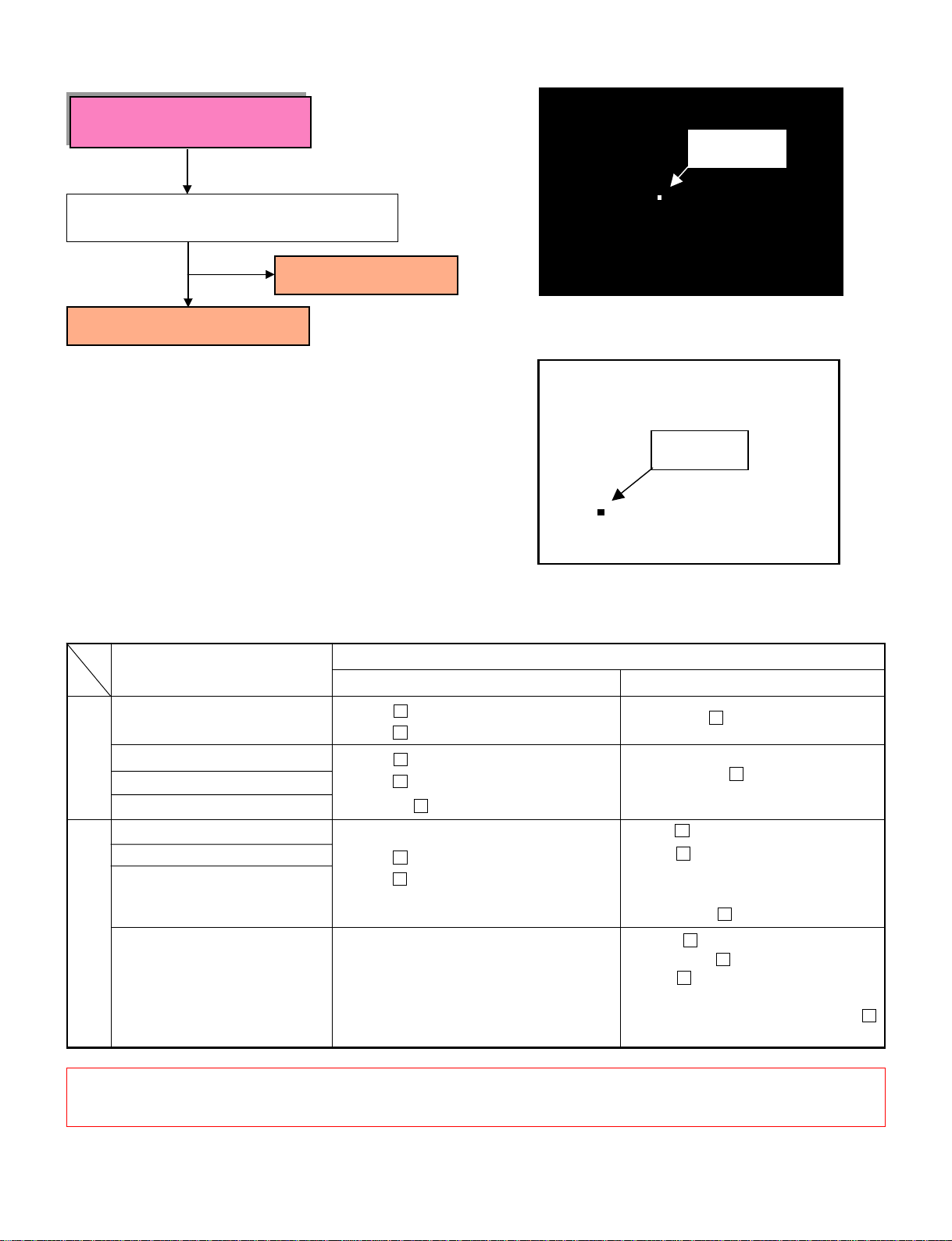
(3) Pixel defect
Pixel defect
Are there many defective pixels exceeding the
pixel defect standard?
Bright defect
N
Y
The PDP is fault.
[Pixel defect standard for reference]
Displayed image
Black all over the screen
(Fig. 1)
Red level 100% over the screen
Green level 100% over the screen
Bright defect
Blue level 100% over the screen Each zone: dots or less for each uni-color
Red level 100% over the screen Zone A: dots or less vertically continuous
Green level 100% over the screen Zone B: dots or less continuous
Blue level 100% over the screen
White all over the screen
Dark defect
(Fig. 2)
This is not a problem.
Pixel defect standard
Non-continuous Continuous
Zone A: dots or less in all for each color
Zone B: dots or less in all for each color
Zone A: dots or less in all for each color
Zone B: dots or less in all for each color
Zone A: dots or less in all for each color
Zone B: dots or less in all for each color
–
(Fig. 1) All-Black Signal
Dark defect
(Fig. 2) All-White Signal
Continuous dots or less
Defective when dots or less are continuously horizontal and seen white.
Except for the continuous portions,
however, the distance between dark
dots shall be cm or more.
Zone A: dots continuous in one
portion or less ( dots for vertical continuity)
Zone B: dots or less continuous
Except for the continuous portions, however,
the distance between dark dots shall be
cm or more.
3-9
Page 16
(Caution1) Zone A: Central part (the area surrounded by
the right and left sides by 1/4H) with
V
Zone B Zone B
ZoneA
the area that is 1/2 of the whole
Zone B: Area other than A above
(4) Wrong lighting
Wrong lighting
1/4H
H
3 dots continuous
→
3 dots continuous
→
4 dots continuous
→
1/4H
(Caution2) The continuous dots appearing in the slantwise
direction or in a cluster state shall be defined
as follows:
The PDP is fault.
All-black signal
Dot errors change
with no continuity.
All-black signal
3-10
Page 17
(5) Dark images [Other than the deterioration in brightness as per (1) above]
The images are dark even with
an all-white input signal.
The PDP is fault.
All-white signal
(6) Defect in horizontal lines
Line defect
The PDP is fault.
All-white signal
All-white signal
3-11
All-white signal
Page 18
Defect in the block unit
The PDP is fault.
All-white signal
(7) Defect in vertical lines
Defect in vertical lines
The PDP is fault.
All-white signal
All-white signal
3-12
All-white signal
Page 19
Block defect
The PDP is fault.
All-white signal
All-white signal
3-13
All-white signal
All-white signal
Page 20

(8) No pictures [(Caution) The voltage outputs of Vs = 170V and Vd = 64V, 5Vdc are always generated, but the LED is
not flashing or lighting for alarming. However, the voltage values can differ according to the PDP.]
No picture is displayed.
Make the setting of OFF→ ON for
the main power supply.
Does the priming glimpse?
NO
YES
When the AD connector is disconnected, is the LVDS signal
normally output to each pin of the
AD connector? (For more details
of the signal, refer to the descriptions about the connector pins.)
YES
The AD connector or the PDP is
fault.
The PDP is fault.
NO
The MAIN PWB is fault.
3-14
Page 21

3. Audio errors
(Caution)In regard to the method of audio input setting, refer to the specifications and the instruction manual to
confirm that all the setting is free from errors. Since then, troubleshooting can be carried out. It must be
noted that the protector functions and no audio output is available if the opposing electrodes of the speaker
output or the speaker output and the ground (GND) are short-circuited. In such a case, turn off the main
power supply and make the connections correctly. The protector is reset when the main power supply is
turned on after that.
Audio errors
YES
In the state that the speaker cable is disconnected, is the audio signal output available at
the speaker terminal?
NO
NO
Is the voltage output specified below available
at each pin of the PA connector in the AUDIO
PWB?
The speaker or the speaker
cable is fault.
The power unit or the PA connector is fault.
Pin No. Name Voltage
1 S+12 12Vdc
2 S+12 12Vdc
3 S+12 12Vdc
4 GND GND
5 GND GND
6 GND GND
YES
Is the waveform specified below output to the
AU connector of the AUDIO PWB?
Pin 6
Pin 7
Pin 5
5Vpp
5Vpp
3.5Vdc
NO
The MAIN PWB or the AU connector is fault.
Pin 1,3 • • • Audio signal waveform
YES
The AUDIO PWB is fault.
3-15
Page 22

4. Remote control not effective
(1) The wired remote control is not effective.
1
When a single item is used
The wired remote control is not effective.
(Caution)The wired remote control is not effective if the setting of
[PLE LINK], [Repeat TIMER], or [IR REMOTE] is ON, or
if the setting of [ID NUMBER] has been made. Therefore, such a setting should be turned off, without fail. Since
then, troubleshooting can be carried out.
Is there a signal output specified below at Pin 7 of the RS connector?
5Vpp
NO
Is there a signal output specified below
at Pin 3 of the M2003? (Refer to the
PWB layout diagram on Page P4-22.)
5Vpp
YES
When the RS connector is disconnected, is there a signal output specified below at the RS connector of the
MAIN PWB?
Pin No. Pin Name Voltage
1 M+7V 6.8Vdc
5 M+5V 5Vdc
YES
NO
NO
The RS connector or the
MAIN PWB is fault.
Is there a 3.3Vdc output at
Pin 2 of the M2003? (Refer
to the PWB layout diagram
on Page P4-22.)
YES
NO
The RS232C PWB is fault.
The RS connector or the
MAIN PWB is fault.
The remote control or the remote
control cable is fault.
YES
The 232C PWB is fault.
2
When a daisy chain (including the video wall) is used
The wired remote control is not effective.
Are the 0Vdc and 5Vdc outputs respectively available at Pins 9 and 10
of the RS connector in the standard
product of 232C PWB?
NO
The MAIN PWB is fault.
YES
Is there a clock signal output at Pin 3 of the M2004?
(Refer to the PWB layout
diagram on Page P4-22.)
NO
The 232C PWB is fault.
3-16
YES
Check the products of second and thereafter according to “1 When a single item
is used.”
Page 23

(2) The wireless remote control is not effective.
(Caution)Since the detection of “wired” or “wireless” is conducted for the remote control through the remote terminal,
it is necessary to pull out the remote control cable from the remote terminal, without fail. Troubleshooting
should be carried out after confirming that “IR REMOTE” is set at ON and that “ID NUMBER” is at ALL
according to the user’s menu.
The wireless remote control is not
effective.
NO
Is there a 0Vdc output at Pin 12 of the RS connector?
YES
Is there a signal output specified below at Pin
6 of the PW connector?
5Vp-p
YES
NO
When the RS connector is disconnected, is
there a 0Vdc output at Pin 12 of the RS connector in the MAIN PWB?
YES
The 232C PWB or the RS con-
NO
The MAIN PWB is fault.
nector is fault.
Is there a signal output specified below at Pin
1 of the LD connector?
5Vp-p
YES
The LED connector or the LED PWB is fault.
YES
The PW connector or the PWR
PWB is fault.
3-17
Page 24

MAIN PWB(HDCP)
IC9501
3-18
Page 25

AUDIO PWB
3-19
Page 26

232C PWB
CTL PWB
PWR PWB
LED PWB
SENB PWB
SENC PWB
SEND PWB
M2003 pin 2
M2004 pin 3
M2003 pin 3
3-20
Page 27

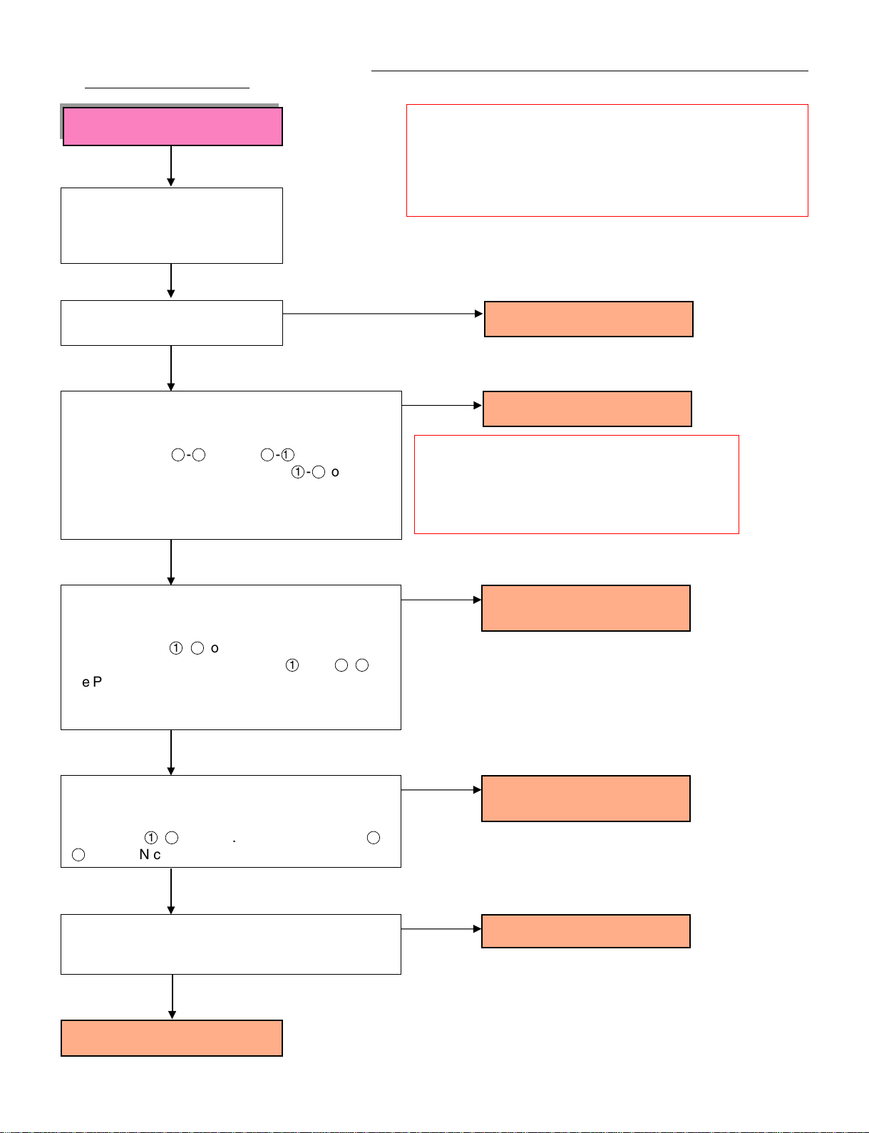
METHOD OF ADJUSTMENTS
■ Adjusting conditions
Adjustments should be carried out in the procedures of A to B specified below. However, any adjustments other than
the items A to B below are not required.
A. When the “PDP module” is replaced, perform adjustment item 1-1 specified on the following page.
B. When the “POWER UNIT” is replaced, perform adjustment item 1-1 specified on the following page.
4-1
Page 28

1-1. For the PD-6130 Series
1-1-1. Adjustment of the Vs voltage
(1) Enter a color bar input by means of either video signal of VIDEO input, or DVD/HD input, or RGB input, and turn
on the power switch of the main unit.
(2) Turn the volume control (RV6) in the power unit and make adjustments until the voltages of CH2 and CH1 (D,
GND) of the power unit attain the voltage values specified for the PDP (Vs value of the voltage regulation indicator label on below the figure) ±1V.
1-1-2. Adjustment of the Vd voltage
(1) Enter a color bar input by means of either video signal of VIDEO input, or DVD/HD input, or RGB input, and turn
on the power switch of the main unit.
(2) Confirm that the voltages of CH4 and CH1 (D, GND) of the power unit are maintained at the voltage values
specified for the PDP (Vd value of the voltage regulation indicator label on below the figure) ±1V.
Otherwise, turn the volume control (RV5) until the voltage attains the voltage values specified for the PDP (Vd
value of the voltage regulation indicator label on below the figure) ±1V.
1-1-3. Adjustment of the +5V voltage
(1) Display a color bar by means of either video signal of VIDEO input, or DVD/HD input, or RGB input.
(2) Confirm that the voltages of CH3 and CH1 (D, GND) of the power unit are maintained at “5.15 ± 0.1V”.
Otherwise, turn the volume control (RV2) until the voltage attains “5.15 ± 0.1V”.
SERIAL NO.
********
Vd= **V
Vs=***V
CODE -01
OR
Vs/Vd/100/185/220 V
555/84.2/782/10204 K
347 W/0 /2 P
(Caution) Rear Side View when the Rear Cover is Removed
The position of label adhesion is subject to change
without notice.
4-2
Page 29

* Top view of the power unit for the PD-6130 Series
P
V
P
M
P
N
P
A
Adjustment
of 5V
RV3
D+3.3 ADJ
CH1
D.GND
RV2
D+5 ADJ
Adjustment of
the Vd voltage
CH3
Vcc
RV5
D+70 ADJ
PH
CH4
Vd
RV6
D+170 ADJ
PD
CH2
Vs
Adjustment of
the Vs voltage
AC
4-3
Page 30

METHOD OF DISASSEMBLY
(Caution)1. Before disassembly, turn power off the main unit and pull out the power plug from the wall outlet.
2. Use a screwdriver with a fitting size. Otherwise, the screw threads may be damaged.
3. Reassembly can be carried out in the reverse order for disassembly. Refer to the disassembly procedures and forward
reassembly in the reverse order.
4. The order for taking out the parts (or components) is indicated by the foregoing numeral that is attached to the name
of each part.
5. The wire connector symbol is indicated by two digits of Marking . Read CN- when examining the table of parts.
6. Class A or Class B in the text is applicable to the models specified below.
CLASS B: PD-6130
1. Outlined method of disassembly
The outlined procedures for the disassembly of the major parts are shown below (disassembled in the direction of ).
In regard to the details of disassembly, cautions, etc., refer to the method of replacement for each part [page indicated in ( )].
SET
(with a STAND)
STAND
(P5-2)
BACK COVER
(P5-3)
CHASSIS ASSY
(P5-4)
PDP
(P5-5)
F-BRACKET(IN)
(P5-6)
FILTER
(P5-6~5-7)
SET
(without a STAND)
* Modification means that the screws are
mounted or removed.
Modifications of
a STAND *
(P5-10)
Modifications of
a BACK COVER *
(P5-11)
BACK COVER
(P5-3)
FRONT PANEL
(P5-9)
F-BRACKET B(OUT)
(P5-8)
TERMINAL PANEL M SUB ASSY
(P5-12)
TERMINAL PANEL S
(P5-14)
COVER SW
(P5-15)
TERMINAL PANEL B SUB ASSY
(P5-16)
POWER UNIT
(P5-18)
SEND PWB
(P5-19)
SENB PWB
(P5-19)
SENC PWB
(P5-19)
F-BRACKET(OUT) ASSY
(P5-7)
LED PWB
(P5-8) (P5-8)
CTL PWB
(P5-8)
TERMINAL PANEL M
(P5-13)
232C PWB
(P5-14)
POWER BUTTON
(P5-15) (P5-15)
TERMINAL PANEL B
(P5-17)
FAN
(P5-19)
COVER CTL
CONTROL BUTTON
(P5-8)
MAIN PWB
(P5-13)
PWR PWB
AUDIO PWB
(P5-17)
AC INLET
(P5-17)
5-1
Page 31

2. STAND
(1)SCREW M6*50 4p
5-2
Page 32

3. BACK COVER
(5)SRW33
PL-CPIMS*4*12*15KF
*27p
(1)SRW34
PL-CPIMS*4*16*3KF
*4p
M31 GS COVER
(Caution) Replacement is
impossible unless the NAME
PLATE is removed.
M03 SERIAL LABEL
(Caution) This is not a service part.
M56 SPEAKER LABEL
(4)SRW32
CBIPS*4*12*15KF
*12p
(2)M18 HANDLE
29F00591 *2p
M57 NAME PLATE
(6)M58 BACK COVER
29P01271
M63 LABEL(EARTH)
(3)SRW35 PL-CPIMS*3*10*15KF
*14p
M55 AC IN LABEL
5-3
Page 33

4. CHASSIS ASSY
(6)SRW05,06 PL-CPIMS*6*20*15KF
*10p
(7)SRW07,08,09,11,13
PL-CPIMS*4*12*15KF
*22p
(4)CONNECTOR
(3) SRW17 TP-M3*6*3KF
(Caution) For mounting, it should
be tightened together with the round
terminal of the AD cable.
(5)CONNECTOR 4p
(Caution) Remove the ferrite
core first.
5-4
(8)CHASSIS ASSY
(2)M40 SHIELD COVER MAIN
(1)SRW31 PL-CPIMS*4*12*15KF
*8p
Page 34

5. PDP
(4)CN-PH CN 9P(PH) 360W,1007-20
(3) CN-PD CN 10P(PD) 920W,1007-20
(5)PDP PDP-NP61C2MF01AA
3S361002
5-5
(2)CN-AD CABLE 31P L320
7S530030
(1)SCREW
(Caution) This screw is used
to fasten the PWB of the PDP.
Positioning pin
Page 35

6. F-BRACKET(IN) /FILTER
(Caution) Once the shielding tape and the cushion are removed, they must not be used again because their adhesive strength
has been reduced.
(4)M33 F-BRACKET T(IN)
M49 CUSHION(686*10*T5)
*4p
* Used in common for top and bottom
M48 CUSHION(782*10*T5)
*2p
* Used in common for right and left
(2)M32 F-BRACKET LR(IN)
2p
* Used in common for right and left
(3)M34 F-BRACKET B(IN)
(5)M54 FILTER
CLASS B :29KS0131
M04 EDGING SADDLE(EDS-1208U)
*2p
(Caution) The filter is standardized to be positioned at bottom left.
M62 SHIELDING TAPE (33MM*50M)
(1)SRW04 PL-CPIMS*3*6*15KF
*30p
5-6
Page 36

8. F-BRACKET(OUT) ASSY
(1)F-BRACKET (OUT) ASSY
M20 CORNER PIECE LT
(Caution) Insertion is possible by sliding it
from bottom to top.
SRW03 CBIPS*4*12*15KF
*8p
(2)FRONT PANEL ASSY
M21 CORNER PIECE RT
(Caution) Insertion is possible by sliding it
from bottom to top.
M36 F-BRACKET T(OUT)
M35 F-BRACKET LR(OUT)
*2p
* Used in common for right and left
M22 CORNER PIECE LB
(Caution) Insertion is possible by sliding it
from top to bottom.
M37 F-BRACKET B(OUT)
M23 CORNER PIECE RB
(Caution) Insertion is possible by sliding it
from top to bottom.
5-7
Page 37

9. LED PWB/CTL PWB/F-BRACKET B(OUT)/COVER CTL/CONTROL BUTTON
(5)CONNECTOR
(2)A04 CTL PWB
936Q0SB1
(Caution) For reassembly, put the CONTROL BUTTON in the
clearance and screw-fasten the CTL PWB to the F-BRACKET.
(1)SRW01 TP-M3*6*3KF
*3p
(3) M26
(4)M24
(6)SRW02 TP-M3*6*3KF
*2p
(8)CONNECTOR
CLASS B CONTROL BUTTON-S: 29G00381
(7)A06 LED PWB
936Q0SD1
CLASS B COVER CTL-S:29F00941
(10)M37 F-BRACKET B(OUT)
(9)M10 CLAMP(UAMS-05-2)
FRONT PANEL ASSY
*7p
5-8
Page 38

10. FRONT PANEL
(2)M16
FRONT PANEL:29D00711
5-9
Page 39

11. STAND (modification)
(6) Fit it, using the screw that
has been removed as per (1).
(Caution) The screw can
be tightened only midway.
(1)SCREW M6*50 2p*2
(3)COVER POST 1p*2
(2)PL-CPIMS*4*12*15KF 1P*2
(5)POST 1p*2
(4)HEXAGONAL BOLT 3p*2
(
(Caution) Use a hexagon head wrench
(opposite side distance 5mm).
5-10
Page 40

12. BACK COVER (modification)
(Caution) The illustration below shows a case when the STAND has been removed.
(1)SRW32
CBIPS*4*12*15KF
*12p
5-11
(2)FRONT PANEL ASSY
Page 41

13. TERMINAL PANEL M SUB ASSY
(7)SRW25 TP-M3*6*3KF
*3p
(8)SRW17 TP-M3*6*3KF
*4p
(3)SRW17 TP-M3*6*3KF
(Caution) It should be tightened
together with the round terminal
of the AD cable.
(9)TERMINAL PANEL M
SUB ASSY
(5)SRW18 TP-M3*6*3KF
*2p
(6)M30 HEAT SINK
(4)CONNECTOR 12p
(2)M40 SHIELD COVER MAIN
(1)SRW31 PL-CPIMS*4*12*15KF
*8p
5-12
Page 42

14. TERMINAL PANEL M/MAIN PWB
(Caution) Please note that no DS connector is furnished even though the MAIN PWB is ordered.
(6)A01 MAIN PWB
936Y2M02
(5)M27 SHIELD PLATE MAIN
(Caution) After sticking the TERMINAL SHEET to
the TERMINAL PANEL, push the peripheral area
of the screw hole to strengthen the adhesion.
(In 3 positions)
(2)SRW15 CBIPS*3*8*3KF
*7p
(1)SRW16 SCREW(UNC4-40/4-40)
*4p
(Caution) Use a hexagon head driver
(opposite side distance 5mm).
5-13
Page 43

15. TERMINAL PANEL S/232C PWB
(4)A03 232C PWB
936Q0SA1
(3)SRW19 SCREW(UNC4-40/4-40)
*2p
(Caution) Use a hexagon head driver
(opposite side distance 5mm).
(Caution) After sticking the TERMINAL
SHEET to the TERMINAL PANEL, push
the peripheral area of the screw hole to
strengthen the adhesion.
(1)SRW20 TP-M3*6*3KF
*2p
(2)SRW26 TP-M3*6*3KF
5-14
Page 44

16. COVER SW/POWER BUTTON/PWR PWB
(1)SRW28 TP-M3*6*3KF
*2p
Rear side
(Caution) Positioning pin
Use it in the case of reassembly.
(3)M25 POWER BUTTON(50XM3)
29G00281
(2)M19 COVER SW
29F00721
(4)A05 PWR PWB
936Q0SC1
5-15
Page 45

17. TERMINAL PANEL B SUB ASSY
(1)CONNECTOR 3p
(3) SRW23 TP-M3*6*3KF
*2p
(5)TERMINAL PANEL B
SUB ASSY
(4)SRW27 TP-M3*6*3KF
*3p
(2)SRW24 ET-CBIMS*4*8*3KF
5-16
Page 46

18. TERMINAL PANEL B/AUDIO PWB/AC INLET
(4) CN-FG CABLE 1P L400
7S530027
(5) CN-PI CN 2-WP(PI) 360W,1672-18
(8)A02 AUDIO PWB ASSY
936R4AA2
(6)E03 AC INLET 10DKDG3S(Y1)
6S760010
(Caution) Mount the INLET so
that its label faces upwards.
(7)SRW21 CBIPS*3*8*3KF
*2p
(2)M17 INLET COLLAR
*2p
(Caution) Insert it between the screw
and the TERMINAL SHEET.
(9)M51 TERMINAL SHIEET B
(10)M42 TERMINAL PANEL B
29H03191
Rear
side
(3)M45 BARRIER(AC INLET)
29J00871
(Caution) Mount it so that its bent
side is positioned upwards.
(1)SRW22 CPIMS*NO.6-32UNC
*8*3GF *2p
(Caution) Positioning hole
For mounting, it should be combined with the embossed
part on the main unit side.
TERMINAL PANEL B
29H03191
5-17
Page 47

19. POWER UNIT
(2)PSU POWER UNIT
3S110161
(1)SRW14 PL-CPIMS*4*12*15KF
*6p
5-18
Page 48

20. SENB PWB/SENC PWB/SEND PWB/FAN
(Caution) For mounting, the FAN should be installed as illustrated.
(2)A07 SENB PWB
936Q0SE1
(7)SRW30 SCREW,M3*30*15KF
*6p
M44 BRACKET PC
2p
(1)SRW29 TP-M3*6*3KF
(8)E01 FAN MOTOR 9G1212M4D03
3S170014 *2p
(9)E02 FAN MOTOR 9G1212M4D04
3S170015
M02 INSULATOR(D4.5**T1)
*2p
(Caution) Stick it to the screw hole
area on the rear side of the PWB.
(4)A09 SEND PWB
936Q0SG1
(3)SRW29 TP-M3*6*3KF
(5)SRW29 TP-M3*6*3KF
M02 INSULATOR(D4.5**T1)
*2p
(Caution) Stick it to the screw hole
area on the rear side of the PWB.
SRW36 PL-CPIMS*4*12*15KF
*4p
5-19
(6)A08 SENC PWB
936Q0SF1
M02 INSULATOR(D4.5**T1)
*2p
(Caution) Stick it to the screw hole
area on the rear side of the PWB.
Page 49

21. BRACKET/SHIELD
(10)M43 SHIELD
CABLE
(Caution) Fix it after the PD
cable has been passed.
(9)M39 BRACKET MAIN
29H03011
(7)SRW08 PL-CPIMS*4*12*15KF
*10p
(Peripheral area of the BRACKET MAIN)
M46 WASHER(6-10)
*2p
(6)SRW12
PL-CPIMS*4*12*15KF
*4p
(SHIELD CABLE)
(8)SRW07 PL-CPIMS*4*12*15KF
*10p
(Peripheral area of the CHASSIS)
(12)M41 FAN BRACKET
(2)SRW 05,06 PL-CPIMS*6*20*15KF
*10p
(3)SRW10 PL-CPIMS*4*12*15KF
*3p
(Peripheral area of the BRACKET FAN)
PL-CPIMS*4*12*15KF
(F-BRACKET LR)
PL-CPIMS*4*12*15KF
(BRACKET SENSOR)
(4)SRW13
*2p
(5)SRW11
*3p
(14)M60 CHASSIS L ASSY
M47 SILICONE SHEET(AUDIO)
(Caution) For mounting, remove the separator.
(11)M38 BRACKET
SENSOR
(13)M59 BRACKET
PS ASSY
(15)M61 CHASSIS R ASSY
(1)SRW09 PL-CPIMS*4*12*15KF
*6p
(Peripheral area of the BRACKET PS)
5-20
Page 50

22. WIRE CLAMP
1M04 EDGING SADDLE(EDS-1208U) 1p
2M05 CLAMP(LCT-1S) 1p
3M06 CLAMP(RBWS-0510D) 24p
4M07 CLAMP(RFCC-625) 1p
5M08 CLAMP(RBWS-1015D) 8p
6M09 CLAMP(RBWS-5N) 1p
7M01 BUSHING,INSULATOR 3p
5-21
Page 51

23. GASKET(CLASS B)
(Caution) Gaskets are used only for the CLASS B model. [For more details, refer to Item 6 of the caution column on P.6-1.]
If replacement is intended, the gasket should be carefully stuck without permitting it to protrude from the BACK COVER when
this BACK COVER is being mounted.
M13 GASKET(L120*10*T10)
7p
M11 GASKET(L30*10*T10)
17p
M15 GASKET(L140*13*T1.5)
4p
M14 GASKET(L30*6*T3)
2p
M12 GASKET(L50*10*T10)
22p
5-22
Page 52

24. WIRING
(Caution) “Turns” in the illustration below denotes the number of cable turns to be wound around the ferrite core.
(Example) 3 turns 3 turns of a cable wound around.
2 Pass TM, FB and FC.
2 Pass TM, FA FB and FC.
3 Pass FA and FB.
AU PV
DS
TM FA FB
4
Pass AU, AD, PM, PN and PV.
Pass the AD and fasten it with the attached harness band.
8
2 Pass PW.
8
Pass RS.
Pass the PW beneath the RS.
2
Pass PW.
Pass LD.
8
PW SW2
RS
3
Pass RS.
LD
2 Pass TM, FB and FC.
8 Pass 2 turns of TM.
2 Pass TM and TR.
Pass TR, FB and FC.
2 Pass x2PD.
2
TM
TR
PD
3 Pass PV, PM and PN.
FC PH
PM
PN
AD
,
Pass PN and PM.
7
PV
PM
PN
PA
6
Pass PV, PM, PN and PA.
8
Pass PV.
,
Pass PD and PH.
7
3 x2, Pass AU and PA.
RS
Pass RS and SW.
3
PW
AU
2 Pass SW.
8 Pass 2 turns of PA.
5 Pass AD.
SW1
2 Pass AU and PA.
2 Pass AC.
AC
PA
AU
2 x2, Pass AU.
2 Pass TR, TS and FC.
2 Pass TR and FC.
PHPD
2 Pass PH.
3Pass PH and PD.
Using the filament tape
(19mm), fasten TR,
FA, and FB.
3 Pass GND and AC.
Pass GND and AC.
7
9 Pass 3 turns of GND.
8 Pass 2 turns of GND.
8 Pass 2 turns of AU.
8 Pass 2 turns of TR.
2 x2, Pass TR and TS.
TR
TS
2 x4, Pass TS.
TS
8 Pass 2 turns of TS.
Pass the LD from the bottom.
2 Pass SW.1
1M04 EDGING SADDLE(EDS-1208U) 1p 6M09 CLAMP(RBWS-5N) 1p
2M06 CLAMP(RBWS-0510D) 24p 7FL11,12,41CORE,FERRITE SFT-72SNB 3p
3M08 CLAMP(RBWS-1015D) 8p 8FL21-29,43FERRITE CORE ZCAT2032-930 10p
4M07 CLAMP(RFCC-625) 1p 9FL42 FERRITE CORE(ESD-R-19) 1p
5M05 CLAMP(LCT-1S) 1p
5-23
Page 53

PARTS LIST
A01 936Y2M02 PWB-MAIN
A02 936R4AA2 PWB-AUDIO ASSY
A03 936Q0SA1 PWB-232C
A04 936Q0SB1 PWB-CTL
A05 936Q0SC1 PWB-PWR SWITCH
A06 936Q0SD1 PWB-PWR LED
A07 936Q0SE1 PWB-SENB
A08 936Q0SF1 PWB-SENC
A09 936Q0SG1 PWB-SEND
CN-AD 7S530030 CABLE- 31P L320
CN-FG 7S530027 CABLE -1P L400
E01 3S170014 FAN-MOTOR (9G1212M4D03)
E02 3S170015 FAN-MOTOR (9G1212M4D043)
M16 29D00711 PANEL-FRONT
M18 29F00591 HANDLE
M19 29F00721 COVER-SW
M24 29F00941 COVER CTL (PD-6130)
M25 29G00281 BUTTON-POWER
M26 29G00381 BUTTON-CONTROL
M42 29H03191 PANEL-TERMINAL
M45 29J00871 BARRIER (AC INLET)
M54 29KS0131 SCREEN SHIELD (FILTER)
M58 29P01271 COVER-BACK (61XM2)
PDP 3S361002 PDP-NP61C2MF01AA (T/A REQ)
PSU 3S110161 PWB-POWER UNIT
Ref. Part Number Description
7S580006 CABLE-D-SUB 15P L1800
7S580010 CABLE-STEREO MINI L3M
7S552001 CORD-POWER AC
I/B PD6130 OWNERS GUIDE
3S120171 REMOTE
6-1
Page 54

CONNECTION DIAGRAMS
TEMP-SENSOR3
SENC PWB
PCB-5032F
SCL5
SDA5
VDD+5V
GND
TEMP-SENSOR2
SEND PWB
TS
1
2
3
4
1
2
3
4
AU : SHIELD-WIRE
SCL5
SDA5
VDD+5V
GND
SCL5
SDA5
VDD+5V
GND
TEMP-SENSOR1
SENB PWB
PCB-5032EPCB-5032G
TR
1
2
3
4
SCL5
SDA5
VDD+5V
GND
SCL5
SDA5
123
VDD+5V
1
2
3
4
GND
4
FAN-A
FAN-CTL
123
GND
F-ALM1
FAN-B
FAN-CTL
123
GND
F-ALM2
FAN-C
FAN-CTL
GND
123
F-ALM3
PDP
123
...
293031
ALARM
D.GND
D.GND
D+5
D.GND
D.GND
D+65
(N.C.)
123456789
D+175
D+175
10
D+175
D+175
(N.C.)
D+65
D.GND
D.GND
D+5
D.GND
123456789
D.GND
AD
PD
PH
PWR PWB
PCB-5032C
REMIN1
LEDCTL1
LEDCTL2
12345
LD
12345
REMIN1
LEDCTL1
LEDCTL2
LED PWB
PCB-5032D
GND
GND
REMIN1
LEDCTL1
M+5V
LEDCTL2
M+5V
SW7
POIN
GND
M+5V
M+7V
DS
M+5V
M+7V
M+7V
GND
M+5V
GND
TXD1
GND
REM
REMIN1
TXD
RXD
1234567
GND
GND
AU-L
1,3,5,6,7pin:shield
AU-R
SCL7
MUTE
MAIN PWB
PCB-5035
LEDCTL1
LEDCTL2
8
1
2
3
4
5
RS
6
7
8
9
10
11
12
SDA7
123
GND
GND
HDSTP
SW7
POIN
1
2
3
4
PW
5
6
7
8
232C PWB
GND
1234567
PCB-5032A
REMIN2/RXD
RESET SW
PLE_CTL
PV
1234567
A+6
A+6
A+12
A.GND
A.GND
A.GND
NC
8
NC
TM
123
SCL5
FA FB
4
GND
SDA5
VDD+5V
M+7V
TXD
GND
123456789
RXD
RS
123
M+5V
GND
F-ALM1
FAN-CTL
GND
REMIN2/RXD
RESET SW
123
GND
F-ALM2
FAN-CTL
1 GND
2 GND
3 ALARM
4 GND
5 PS+
6 PS 7 MSEL
8 GND
9 RH+
10 RH11 RG+
12 RG13 RF+
14 RF15 GND
16 RE+
17 RE18 RD+
19 RD20 RCLK+
PLE_CTL
TXD1
GND
101112
FC
REM
123
D.GND
GND
POWER
D.GND
F-ALM3
FAN-CTL
POMUTE
D.GND
D.GND
D.GND
D.GND
D.GND
D.GND
21 RCLK22 GND
23 RC+
24 RC25 RB+
26 RB27 RA+
28 RA29 GND
30 GND
31 GND
CTL1
123
SW
M+7V
SW7
NC
D+3.3
D+3.3
D+3.3
D+2.5
D+2.5
D+2.5
CTL2
GND
10
11
12
29
30
31
123456789
1
2
3
4
5
6
7
1
2
3
4
5
6
7
8
9
1
2
3
.
AD
.
.
PM
PN
PV
PA
1
2
3
4
5
6
7
1
2
3
4
5
6
7
8
9
10
11
12
1
2
3
4
5
6
7
8
1
2
3
4
5
6
M+7V
D.GND
POWER
D.GND
POMUTE
SW7
NC
D+3.3
D+3.3
D+3.3
D.GND
D.GND
D.GND
D+2.5
D+2.5
D+2.5
D.GND
D.GND
D.GND
A+12
A.GND
A+6
A+6
A.GND
A.GND
NC
NC
S+12
S+12
S+12
GND
GND
GND
D+5
D+65
D.GND
D.GND
(N.C.)
D.GND
D.GND
ALARM
POWER SUPPLY
D+175
123456789
10
D+175
D+175
D+175
D+65
(N.C.)
D.GND
D.GND
D+5
D.GND
D.GND
L
N
AC
1
2
AU : SHIELD-WIRE
PA
AUDIO PWB
PCB-5033
ROUT+
ROUT-
LOUT+
LOUT-
123
4
SPEAKER_OUT
12345
S+12
SW
S+12
1
2
3
S+12
GND
GND
CTL1
CTL2
GND
6
AU-L
GND
AU-R
GND
GND
MUTE
SCL7
SDA7
PCB-5032B
1
2
3
4
5
6
7
CTL PWB
AU
7-1
Page 55

CONNECTOR PIN EXPLANATION
PD-6130 Series
(Caution) The operating voltages specified below are used in common irrespective of the presence of signals. In this case, how-
ever, part of the operating voltages (red characters) may change according to the signal conditions when the main
power supply is turned on (POWER button ON).
Status of LED lighting: v for lighting in green, vv for unlighting, and vvv for lighting in red.
Basic operation (Numerical unit: Vdc; except for the case when units are individually indicated)
Name Pin No. Pin name Function
PN
PM
PV
DS
AU
RS
1 D+3.3
2 D+3.3
3 D+3.3
4D.GNDGND 000000––
5D.GNDGND 000000––
6D.GNDGND 000000––
7 D+2.5
8 D+2.5
9 D+2.5
10D.GNDGND 000000––
11D.GNDGND 000000––
12D.GNDGND 000000––
1 M+7
2D.GNDGND 000000––
3 POWER Power control 0 4.9 4.9 0 0 0 – MAIN→POWER
4D.GNDGND 000000––
5 POMUTE Mute signal for AC power OFF 4.8 4.8 4.8 4.8 4.8 4.8 4.8→ POWER→MAIN
6 SW7 Power start control 0 6.8 6.8 6.8 6.8 0 – POWER→MAIN
7 NC Non-connection terminal – – – – – – – –
1 A+12V
2A.GNDGND 000000––
3 A+6
4 A+6
5A.GNDGND 000000––
6A.GNDGND 000000––
7 NC No-connection terminal – – – – – – – –
8 NC No-connection terminal – – – – – – – –
1 GND GND 0 0 0 0 0 0 – –
2 HDSTP
3 GND GND 0 0 0 0 0 0 – –
1 AU_L Audio signal L CH 0
2 GND GND 0 0 0 0 0 0 – –
3 AU_R Audio signal R CH 0
4 GND GND 0 0 0 0 0 0 – –
5 MUTE Mute signal of audio output 3.5 3.5→0 3.5→0 3.5 3.5→0 3.5 3.5→0 MAIN→AUDIO
6 SCL7 Clock line of the I2C bus 0 Clock signal Clock signal 0 0 0 – MAIN→AUDIO
7 SDA7 Data line of the I2C bus 0 Clock signal Clock signal 0 1 0 – MAIN→AUDIO
1 M+7V
2 TXD RS232 driver output 5 5 5 5 5 5 – MAIN→RS232C
3 GND GND 0 0 0 0 0 0 – –
4 RXD RS232 receiver input 0 Clock signal Clock signal Clock signal 0 0 – RS232C→MAIN
5 M+5V
6 GND GND 0 0 0 0 0 0 – –
7
REMIN2/RXD1
8 RESET SW NC – – – – – – – –
9 PLE_CTL PLE control 0 Clock signal Clock signal Clock signal 0 0 – MAIN→RS232C
3.3V power supply for digital circuits
3.3V power supply for digital circuits
3.3V power supply for digital circuits
2.5V power supply for digital circuits
2.5V power supply for digital circuits
2.5V power supply for digital circuits
7V power supply for microcomputer
12V power supply for analog circuits
6V power supply for analog circuits
6V power supply for analog circuits
Video mute control for chroma signals
7V power supply for microcomputer
5V power supply for microcomputer
Data signal of wired remote control
AC power ON
(Power cord
connected to
the wall outlet)
vv
6.8 6.8 6.8 6.8 6.8 6.8 – POWER→MAIN
6.8 6.8 6.8 6.8 6.8 6.8 – MAIN→RS232C
Main power ON
(POWER button ON)
No signal With signal
0 3.3 3.3 0 0 0 – POWER→MAIN
0 3.3 3.3 0 0 0 – POWER→MAIN
0 3.3 3.3 0 0 0 – POWER→MAIN
0 2.5 2.5 0 0 0 – POWER→MAIN
0 2.5 2.5 0 0 0 – POWER→MAIN
0 2.5 2.5 0 0 0 – POWER→MAIN
0 12 12 0 0 0 – POWER→MAIN
0 6 6 0 0 0 – POWER→MAIN
0 6 6 0 0 0 – POWER→MAIN
0 0V when the 0V when the 0V when the 0V when the 0 – –
DS connector DS connector DS connector DS connector
is connected; is connected; is connected; is connected;
High-Z when High-Z when High-Z when High-Z when
it is not conn- it is not conn- it is not conn- it is not connected ected ected ected
(Video mute) (Video mute) (Video mute) (Video mute)
Selected input Selected input
signals are out- signals are output. put.
Selected input Selected input
signals are out- signals are output. put.
(5Vac) when (5Vac) when
data are rec- data are received; 5Vdc eived; 5Vdc
when no data when no data
are received. are received.
(5Vac) when (5Vac) when
data are rec- data are received; 5Vdc eived; 5Vdc
when no data when no data
are received. are received.
(5Vac) when (5Vac) when (5Vac) when
data are rec- data are rec- data are received; 5Vdc eived; 5Vdc eived; 5Vdc
when no data when no data when no data
are received. are received. are received.
055550–MAIN→RS232C
0 Clock signal Clock signal Clock signal 0 0 – RS232C→MAIN
(5Vac) when (5Vac) when (5Vac) when
data are rec- data are rec- data are received; 5Vdc eived; 5Vdc eived; 5Vdc
when no data when no data when no data
are received. are received. are received.
(5Vac) when (5Vac) when (5Vac) when
data are rec- data are rec- data are received; 5Vdc eived; 5Vdc eived; 5Vdc
when no data when no data when no data
are received. are received. are received.
v
management
Power
vvv
Standby
vvv
0 0 0 – MAIN→AUDIO
0 0 0 – MAIN→AUDIO
Main power
vv
OFF
AC power OFF
(Power cord
pulled out of the
wall outlet)
vv
Signal direction
Ver. 1
7-2
Page 56

Name Pin No. Pin name Function
10 TXD1 RS232 driver output 0 Clock signal Clock signal Clock signal 0 0 – MAIN→RS232C
11 GND GND 0 0 0 0 0 0 – –
TM
TR
TS
FA
FB
12 REM
1 SCL5 Clock line of the I2C bus 0 Clock signal Clock signal Clock signal 0 0 – MAIN→SENB
2 SDA5 Data line of the I2C bus 0 Clock signal Clock signal Clock signal 0 0 – MAIN←→SENB
3 VDD+5V
4 GND GND 0 0 0 0 0 0 – –
1 SCL5
2 SDA5
3 VDD+5V
4 GND GND 0 0 0 0 0 0 0 –
1 SCL5
2 SDA5
3 VDD+5V
4 GND GND 0 0 0 0 0 0 0 –
1 FAN-CTL Voltage-controllable 0 9.3Vdc during 9.3Vdc during 0 0 0 – MAIN→FAN
2 GND GND 0 0 0 0 0 0 – –
3 ALARM FAN lock detect 0 0V during nor- 0V during nor- 0 0 0 – FAN→MAIN
1 FAN-CTL Voltage-controllable 0 9.3Vdc during 9.3Vdc during 0 0 0 – MAIN→FAN
2 GND GND 0 0 0 0 0 0 – –
Insertion detection for wired remote control input
5V power supply for analog signals
I2C bus clock for temperature sensors
I2C bus data for temperature sensors
5V power supply for analog signals
I2C bus clock for temperature sensors
I2C bus data for temperature sensors
5V power supply for analog signals
power supply high-speed high-speed
signal output
power supply high-speed high-speed
Basic operation (Numerical unit: Vdc; except for the case when units are individually indicated)
AC power ON
(Power cord
connected to
the wall outlet)
vv
Main power ON
(POWER button ON)
No signal With signal
(5Vac) when (5Vac) when (5Vac) when
data are rec- data are rec- data are received; 5Vdc eived; 5Vdc eived; 5Vdc
when no data when no data when no data
are received. are received. are received.
0 5V when the 5V when the 5V when the 0 0 – RS232C→MAIN
wired remote wired remote wired remote
control is co- control is co- control is connected; 0V nnected; 0V nnected; 0V
when no wired when no wired when no wired
remote control remote control remote control
is connected. is connected. is connected.
(5Vac) when (5Vac) when (5Vac) when
data are rec- data are rec- data are received; 5Vdc eived; 5Vdc eived; 5Vdc
when no data when no data when no data
are received. are received. are received.
(5Vac) when (5Vac) when (5Vac) when
data are rec- data are rec- data are received; 5Vdc eived; 5Vdc eived; 5Vdc
when no data when no data when no data
are received. are received. are received.
0 5 5 0 0 0 – MAIN→SENB
0 Clock signal Clock signal Clock signal 0 0 – SENB←→SEND
(5Vac) when (5Vac) when (5Vac) when
data are rec- data are rec- data are received; 5Vdc eived; 5Vdc eived; 5Vdc
when no data when no data when no data
are received. are received. are received.
0 Clock signal Clock signal Clock signal 0 0 – SENB←→SEND
(5Vac) when (5Vac) when (5Vac) when
data are rec- data are rec- data are received; 5Vdc eived; 5Vdc eived; 5Vdc
when no data when no data when no data
are received. are received. are received.
0 5 5 0 0 0 – SENB→SEND
0 Clock signal Clock signal Clock signal 0 0 – SEND←→SENC
(5Vac) when (5Vac) when (5Vac) when
data are rec- data are rec- data are received; 5Vdc eived; 5Vdc eived; 5Vdc
when no data when no data when no data
are received. are received. are received.
0 Clock signal Clock signal Clock signal 0 0 – SEND←→SENDC
(5Vac) when (5Vac) when (5Vac) when
data are rec- data are rec- data are received; 5Vdc eived; 5Vdc eived; 5Vdc
when no data when no data when no data
are received. are received. are received.
0 5 5 0 0 0 – SEND→SENC
revolution revolution
(Fan mode H); (Fan mode H);
7.6Vdc during 7.6Vdc during
medium- mediumspeed revolu- speed revolution (Fan tion (Fan
mode M); mode M);
5.2Vdc during 5.3Vdc during
low-speed low-speed
revolution revolution
(Fan mode L) (Fan mode L)
mal fan opera- mal fan operation; 5Vdc tion; 5Vdc
while the fan while the fan
is stopped. is stopped.
revolution revolution
(Fan mode H); (Fan mode H);
7.6Vdc during 7.6Vdc during
medium- mediumspeed revolu- speed revolution (Fan tion (Fan
mode M); mode M);
5.2Vdc during 5.3Vdc during
low-speed low-speed
revolution revolution
(Fan mode L) (Fan mode L)
v
management
Power
vvv
Standby
vvv
Main power
vv
OFF
AC power OFF
(Power cord
pulled out of the
wall outlet)
vv
Signal direction
7-3
Page 57

Name Pin No. Pin name Function
3 ALARM FAN lock detect 0 0V during nor- 0V during nor- 0 0 0 – FAN→MAIN
FC
AD
1 FAN-CTL Voltage-controllable 0 9.3Vdc during 9.3Vdc during 0 0 0 – MAIN→FAN
2 GND GND 0 0 0 0 0 0 – –
3 ALARM FAN lock detect 0 0V during nor- 0V during nor- 0 0 0 – FAN→MAIN
1 GND GND 0 0 0 0 0 0 – –
2 GND GND 0 0 0 0 0 0 – –
3 ALARM Module alarm signal 0 5Vdc during 5Vdc during 0 0 0 – PDP→MAIN
4 GND GND 0 0 0 0 0 0 – –
5 PS+ PSS input PS+ 0 PSS LVDS PSS LVDS 0 0 0 – PDP→MAIN
6 PS– PSS input PS– 0 PSS LVDS PSS LVDS 0 0 0 – PDP→MAIN
7 MSEL 42V5 compatible interface OFF 0 0 0 0 0 0 – –
8 GND GND 0 0 0 0 0 0 – –
9 RH+ OSD system output H+ 0 OSD LVDS OSD LVDS 0 0 0 – MAIN→PDP
10 RH– OSD system output H– 0 OSD LVDS OSD LVDS 0 0 0 – MAIN→PDP
11 RG+ OSD system output G+ 0 OSD LVDS OSD LVDS 0 0 0 – MAIN→PDP
12 RG– OSD system output G– 0 OSD LVDS OSD LVDS 0 0 0 – MAIN→PDP
13 RF+ Mode system output F+ 0 Video mode Video mode 0 0 0 – MAIN→PDP
14 RF– Mode system output F– 0 Video mode Video mode 0 0 0 – MAIN→PDP
15 GND GND 0 0 0 0 0 0 – –
16 RE+ Video system output E+ 0 Video data Video data 0 0 0 – MAIN→PDP
signal output
power supply high-speed high-speed
signal output
Basic operation (Numerical unit: Vdc; except for the case when units are individually indicated)
AC power ON
(Power cord
connected to
the wall outlet)
vv
Main power ON
(POWER button ON)
No signal With signal
mal fan opera- mal fan operation; 5Vdc tion; 5Vdc
while the fan while the fan
is stopped. is stopped.
revolution revolution
(Fan mode H); (Fan mode H);
7.6Vdc during 7.6Vdc during
medium- mediumspeed revolu- speed revolution (Fan tion (Fan
mode M); mode M);
5.2Vdc during 5.3Vdc during
low-speed low-speed
revolution revolution
(Fan mode L) (Fan mode L)
mal fan opera- mal fan operation; 5Vdc tion; 5Vdc
while the fan while the fan
is stopped. is stopped.
normal PDP normal PDP
operation; 0V operation; 0V
when the PDP when the PDP
is out of order. is out of order.
serial differen serial differen
tial PS+ input tial PS+ input
0Vac; Bias 0.3Vac; Bias
1.1Vdc 1.25Vdc
serial differen serial differen
tial PS+ input tial PS+ input
0Vac; Bias 0.3Vac; Bias
1.4Vdc 1.25Vdc
serial differen- serial differential H+ output tial H+ output
0Vac; Bias 0Vac; Bias
1.1Vdc 1.1Vdc
serial differen- serial differential H– output tial H– output
0Vac; Bias 0Vac; Bias
1.41Vdc 1.4Vdc
serial differen- serial differential G+ output tial G+ output
0.3Vac; Bias 0.3Vac; Bias
1.25Vdc 1.25Vdc
serial differen- serial differential G– output tial G– output
0.3Vac; Bias 0.3Vac; Bias
1.25Vdc 1.25Vdc
LVDS serial LVDS serial
differential F+ differential F+
output 0.3Vac; output 0.3Vac;
Bias 1.25Vdc Bias 1.25Vdc
LVDS serial LVDS serial
differential F– differential F–
output 0.3Vac; output 0.3Vac;
Bias 1.25Vdc Bias 1.25Vdc
LVDS serial LVDS serial
differential E+ differential E+
output 0Vac; output 0Vac;
Bias 1.1Vdc Bias 1.1Vdc
v
*Only for the
PX-42VP4V
Series, 0.3Vac
and bias 1.25
Vdc in theater
mode when 60Hz
motion pictures
are displayed.
Power
management
vvv
Standby
vvv
Main power
OFF
vv
AC power OFF
(Power cord
pulled out of the
wall outlet)
vv
Signal direction
7-4
Page 58

Name Pin No. Pin name Function
17 RE– Video system output E– 0 Video data Video data 0 0 0 – MAIN→PDP
18 RD+ Video system output D+ 0 Video data Video data 0 0 0 – MAIN→PDP
19 RD– Video system output D– 0 Video data Video data 0 0 0 – MAIN→PDP
20 RCLK+ Video system output clock+ 0 Video data Video data 0 0 0 – MAIN→PDP
21 RCLK– Video system output clock– 0 Video data Video data 0 0 0 – MAIN→PDP
22 GND GND 0 0 0 0 0 0 – –
23 RC+ Video system output C+ 0 Video data Video data 0 0 0 – MAIN→PDP
24 RC– Video system output C– 0 Video data Video data 0 0 0 – MAIN→PDP
25 RB+ Video system output B+ 0 Video data Video data 0 0 0 – MAIN→PDP
26 RB– Video system output B– 0 Video data Video data 0 0 0 – MAIN→PDP
27 RA+ Video system output A+ 0 Video data Video data 0 0 0 – MAIN→PDP
28 RA– Video system output A– 0 Video data Video data 0 0 0 – MAIN→PDP
29 GND GND 0 0 0 0 0 0 – –
30 GND GND 0 0 0 0 0 0 – –
31 GND GND 0 0 0 0 0 0 – –
1 REMIN1 Infrared remote control data 0 Clock signal Clock signal Clock signal 0 0 – LED→PWR
LD
2 LEDCTL1 Standby LED control 0 0 0 5 5 0 – PWR→LED
3 LEDCTL2 Standby LED control 5 5 5 5 0 5 – PWR→LED
4 GND GND 0 0 0 0 0 0 – –
5 M+5V
5V power supply for microcomputer
Basic operation (Numerical unit: Vdc; except for the case when units are individually indicated)
AC power ON
(Power cord
connected to
the wall outlet)
vv
Main power ON
(POWER button ON)
No signal With signal
LVDS serial LVDS serial
differential E– differential E–
output 0Vac; output 0.3Vac;
Bias 1.4Vdc Bias 1.25Vdc
LVDS serial LVDS serial
differentialD+ differential D+
output 0Vac; output 0.3Vac;
Bias 1.1Vdc Bias 1.25Vdc
LVDS serial LVDS serial
differential D– differential D–
output 0Vac; output 0.3Vac;
Bias 1.4Vdc Bias 1.25Vdc
clock LVDS clock LVDS
serial differen- serial differential clock+ out- tial clock+ output 0.3Vac; put 0.3Vac;
Bias 1.25Vdc Bias 1.25Vdc
clock LVDS clock LVDS
serial differen- serial differential clock– out- tial clock– output 0.3Vac; put 0.3Vac;
Bias 1.25Vdc Bias 1.25Vdc
LVDS serial LVDS serial
differential C+ differential C+
output 0.3Vac; output 0.3Vac;
Bias 1.25Vdc Bias 1.25Vdc
LVDS serial LVDS serial
differentia C– differential C–
output 0.3Vac; output 0.3Vac;
Bias 1.25Vdc Bias 1.25Vdc
LVDS serial LVDS serial
differential B+ differential B+
output 0Vac; output 0.3Vac;
Bias 1.1Vdc Bias 1.25Vdc
LVDS serial LVDS serial
differentia B– differential B–
output 0Vac; output 0.3Vac;
Bias 1.4Vdc Bias 1.25Vdc
LVDS serial LVDS serial
differential A+ differential A+
output 0Vac; output 0.3Vac;
Bias 1.1Vdc Bias 1.25Vdc
LVDS serial LVDS serial
differentia A– differential A–
output 0Vac; output 0.3Vac;
Bias 1.4Vdc Bias 1.25Vdc
(5Vac) when (5Vac) when (5Vac) when
data are re- data are re- data are received; 5Vdc ceived; 5Vdc ceived; 5Vdc
when no data when no data when no data
are received. are received. are received.
055500–PWR→LED
v
*Only for the
PX-42VP4V
Series, 0.3Vac
and bias 1.25
Vdc in theater
mode when 60Hz
motion pictures
are displayed.
Power
management
vvv
Standby
vvv
Main power
vv
OFF
AC power OFF
(Power cord
pulled out of the
wall outlet)
Signal direction
vv
7-5
Page 59

Name Pin No. Pin name Function
PW
SW
PA
PD
PH
1 SW7 Power start control 0 6.8 6.8 0 0 0 – PW→MAIN
2 POIN Power start detection 0 5 5 5 5 0 – PW→MAIN
3 GND GND 0 0 0 0 0 0 – –
4 M+5V
5 M+7V
6 REMIN1 Infrared remote control data 0 Clock signal Clock signal Clock signal 0 0 – PW→MAIN
7 LEDCTL1 Standby red LED control 0 0 0 5 5 0 – MAIN→PW
8 LEDCTL2 Standby green LED control 0 5 5 5 0 0 – MAIN→PW
1 CTL1 Key input detection 0 1~4.2Vdc 1~4.2Vdc 1~4.2Vdc 0 0 – SW→MAIN
2 CTL2 Key input detection 0 1~4.2Vdc 1~4.2Vdc 1~4.2Vdc 0 0 – SW→MAIN
3 GND GND 0 0 0 0 0 0 – –
1 S+12
2 S+12
3 S+12
4 GND GND 0 0 0 0 0 0 – –
5 GND GND 0 0 0 0 0 0 – –
6 GND GND 0 0 0 0 0 0 – –
1 ALARM PDP alarm signal 0 5Vdc when 5Vdc when 0 0 0 – PDP→POWER
2D.GNDGND 000000––
3D.GNDGND 000000––
4 D.+5
5D.GNDGND 000000––
6D.GNDGND 000000––
7 D+65 Vd power supply for PDP 0 65Vdc (chan- 65Vdc (chan- 0 0 0 – POWER→PDP
8 NC Non-connection terminal – – – – – – – –
9 D+175 Vs power supply for PDP 0 175Vdc (cha- 175Vdc (cha- 0 0 0 – POWER→PDP
10 D+175 Vs power supply for PDP 0 175Vdc (cha- 175Vdc (cha- 0 0 0 – POWER→PDP
1 D+175 Vs power supply for PDP 0 175Vdc (cha- 175Vdc (cha- 0 0 0 – POWER→PDP
2 D+175 Vs power supply for PDP 0 175Vdc (cha- 175Vdc (cha- 0 0 0 – POWER→PDP
3 NC Non-connection terminal – – – – – – – –
4 D+65 Vd power supply for PDP 0 65Vdc (chan- 65Vdc (chan- 0 0 0 – POWER→PDP
5D.GNDGND 000000––
6D.GNDGND 000000––
7 D+5
8D.GNDGND 000000––
9D.GNDGND 000000––
5V power supply for microcomputer
7V power supply for microcomputer
+12V power supply for audio circuits
+12V power supply for audio circuits
+12V power supply for audio circuits
5V power supply for digital circuits
digital circuits geable acco- geable acco-
high-voltage circuits ngeable acc- ngeable acc-
high-voltage circuits ngeable acc- ngeable acc-
high-voltage circuits ngeable acc- ngeable acc-
high-voltage circuits ngeable acc- ngeable acc-
digital circuits geable acco- geable acco-
5V power supply for digital circuits
Basic operation (Numerical unit: Vdc; except for the case when units are individually indicated)
AC power ON
(Power cord
connected to
the wall outlet)
vv
Main power ON
(POWER button ON)
No signal With signal
0 5 5 5 5 0 – MAIN→PW
0 6.8 6.8 6.8 6.8 6.8 – MAIN→PW
(5Vac) when (5Vac) when (5Vac) when
data are re- data are re- data are received; 5Vdc ceived; 5Vdc ceived; 5Vdc
when no data when no data when no data
are received. are received. are received.
when key in- when key in- when key inputs are en- puts are en- puts are entered; 5Vdc tered; 5Vdc tered; 5Vdc
when no key when no key when no key
inputs are inputs are inputs are
entered. entered. entered.
when key in- when key in- when key inputs are en- puts are en- puts are entered; 5Vdc tered; 5Vdc tered; 5Vdc
when no key when no key when no key
inputs are inputs are inputs are
entered. entered. entered.
0 12 12 0 0 0 – POWER→AUDIO
0 12 12 0 0 0 – POWER→AUDIO
0 12 12 0 0 0 – POWER→AUDIO
the PDP is the PDP is
normal; 0V normal; 0V
when it is when it is
abnormal. abnormal.
0 5.15 5.15 0 0 0 – POWER→PDP
ding to the ding to the
PDP) PDP)
ording to the ording to the
PDP) PDP)
ording to the ording to the
PDP) PDP)
ording to the ording to the
PDP) PDP)
ording to the ording to the
PDP) PDP)
ding to the ding to the
PDP) PDP)
0 5.15 5.15 0 0 0 – POWER→PDP
v
management
Power
vvv
Standby
vvv
Main power
vv
OFF
AC power OFF
(Power cord
pulled out of the
wall outlet)
Signal direction
vv
7-6
Page 60

BLOCK DIAGRAMS
Power supply
When the power cord is connected to a wall outlet, M+7V (7Vdc) begins to be fed to IC9503 (M+5V) from Pin 1 of the
PM connector. When the main power switch (S2601) is turned on, IC9503 is turned on by means of SW7 (M+7V) and
M+5V (5Vdc) is fed to the CPU (IC9501). With the power supply of M+5V, the CPU feeds the POWER signal [H] to the
power unit from Pin 3 of the PM connector. As a result, power supplies of the signal system (D+5V, D+3.3V, D+2.5V,
A+12V, A+6V, S+12V) are turned on so that power can be fed to the respective circuits of the signal system. After the
power has been fed to the signal system, the power supplies for the high-voltage system [Vs, Vd
generated and fed to the PDP (plasma display panel).
Sequence
circuit
POWER
(Caution 1)] are
IC9503
M+5V
S2601
AC IN
(AC Connector 1, 2pin)
POMUTE
(PM Connector 5pin)
M+7V
(PM Connector 1pin)
SW7 (PM Connector
6pin) (S2601)
M+5V
(PW Connector 4pin)
AC
Input
(Caution 1) The standard voltages of
Vd and Vs for each model are specified
below. These values can, however,
differ according to the PDP
specifications.
PD-6130 Series Vs=175V,Vd=65V
(Caution 2)
PD-6130 Series T4/5
Input
Filter
Rectifier
Circuit
Power
Factor
Circuit
T1
T2
(Caution 2)
T4
T5
T3
M+7V
Dropper
A+12V
Dropper
S+12V
Dropper
A+6V
D+5V
Vs
Vd
Chopper reg
Dropper
GND
POWER
(PM Connector 3pin)
D+5V
(PH Connector 1, 2pin)
* PD-6130 Series only
(PD Connector 4pin)
A+12V
(PV Connector 1pin)
S+12V
(PA Connector 1~3pin)
A+6V(PV Connector
3, 4pin) VDD+5V
(TM Connector 3pin)
D+2.5V
D+2.5V
(DN Connector 7~9pin)
D+3.3V
D+3.3V
(DN Connector 1~3pin)
V s
(PD Connector 9, 10pin)
Vd
(PD Connector 6, 7pin)
* PD-6130 Series only
(PD Connector 7pin)
ALARM
(PD Connector 1pin)
8-1
Page 61

ANALOG BLOCK DIAGRAM
M5001
VIDEO 1
[BNC]
VIDEO 2
[PHONO]
VIDEO 3
[S-Video]
M5002
M5003
DVD1/HD1
(DVD)
[PHONO]
M5006
AUDIO 1
[PHONO]
M5007
AUDIO 2
[PHONO]
M5008
AUDIO 3
[PHONO]
M5004
RGB1
(PC1)
[Min_D-sub 15pin]
Loop out
M5005
RGB2/DVD2/HD2
(PC2)
[BNC]
M7001
RGB3
(PC3)
[DVI-D]
L
R
L
R
L
R
VD(PC2)
VD2(PC2)
Y IN
C IN
VD
SCL,SDA
VD(PC1)
SEL
IC5170
SN74AHC2
G66
VD2(PC2)
RGB/YUV
(PC2)
HD(PC2)
Analog video signal
Digital video signal
Single Line
Two or more Lines
Loop out
Amp.& Buff
PNP
IC5003
24LCS21AT
RGB/YUV(PC1)
RGB/YUV(PC2)
HD(PC1)
Reform
OPA2356
VD(PC1)
Reform
IC5004
BA10393
YUV
AUDIO 1-3
From CPU
PNPWE
/SN
HD(PC2)
IC5005
From CPU
THRU_ON
RL5001,5002
From IC5708
V_SW_1/2
V_SW_3
Video SEL
(6dB amp. Out)
IC5001
MM1118
THRU_ON
From CPU
AMP
IC5401
AD8013
YUV(DVD)
RGB/YUV
(PC2)
VD(PC1)
VD(PC2)
HD(PC1)
HD(PC2)
DVI signal
From CPU
AUSEL1
Audio SEL
IC5403,IC5404
From IC5708
HD1_ON
DVD/PC2
SELECT
AUSEL2
MM1113
RGB/YUV(PC1)
From CPU
PS_SW
Switch
IC5701
M61323
FL5001
LPF
6MHz
FL5150
LPF
6MHz
Scart_HV
DVD_Y
From IC5708
Sync
on
Green/Y
VIDEO 1,3 IN
VIDEO2 IN
DVD2 IN
DVD1 IN
From CPU
PS SW
PC1
DVD/
PC1/PC2
SELECT
Switch
IC5702
M61323
VD
VD(PC3)
HD(PC3)
From IC5708
PC2/HD2
Video proccesor
IC6001
UPD64011
RGB/HD/DTV/DVD
PC/720P
From IC5708
PC1/2_ON
HD/VD
Select
Switch
IC5706
SN74AHC
2G66
From IC5708
SOG_HD_ON
VD
Select
Switch
IC5707
SN74AHC
2G66
PC3 PC1
VD
Sync on
Green/Y
HD
Select
Switch
IC5705
SN74AHC
2G66
VD
HD
HD
AMP
IC5703
AD8013
VSIN
Sync.
Sep.
VIN
IC5712
BA7078
HSIN
SDA3, SCL3
MEMORY
IC6002
K4S16122D
DIGITAL (S_CLK/S-HSI/S-VSI/DEI 4 Bit)
DIGITAL( YCbCr 10 Bit)
FL6501-6503
DTV/HD
LPF
18MHz
LPF
RGB/DVD
8MHz
FL6504-6506
23MHz
Filter sw
Q6507
Q6509
Q6511
23MHz
720P
DIGITAL
(S-HSI/S-VSI)
[HD/VD]
23M
From CPU
MSYNCTL
From CPU
VIDEO/RGB/
YUV
select
IC5710
SN74HC153
HD / VD
From CPU
VIDEO/RGB/
YUV
select
IC5711
74ACTQ153
PCH_POL
PCH_STATE
PCV_STATE
PCV_POL
To CPU
Picture&
sync cont.
M62320
V_SW_1/2
V_SW_3
PC1
PC2/HD2
PC3
HD1_ON
PC1/2ON
SOG_HD_ON
SCL4, SDA4
From CPU
8M
SELECT
Switch
IC6504-6506
SN74AHC2G66
sync.
SYNCTL
sync.
From CPU
SCL7, SDA7,SMUTE
Selected L/R
IC5708
18M
To/from CPU
CLK/HD
/VD/DE
YCbCr
YUV
RGB
MVD
MHD
HD
VD
DVIHD
DVIVD
DVIRGB
"AU"
AUDIO PWB
Audio
controller
IC3002
BD3869
Audio
amplifire
IC3003
TA2024
+ - - +
SPEAKER TERMINAL
MAIN PWB(1/2)
TO DIGITAL BLOCK
8-2
Page 62

DIGITAL BLOCK DIAGRAM (HDCP)
CTL1/2
(CPU/MUTE)
To/from CPU
LVDS
TMDS_RST
LED PWB
LEDCTL1/2
REMIN1
PWR PWB
“LD”
CTL PWB
232C PWB
REMIN2
PLE_CTL/REM
RXD/TXD
SW7
“SW”
“RS”
MAIN PWB(2/2)
CLK/HD
/VD/DE
YCbCr
YUV
RGB
MVD
MHD
HD
FROM ANALOG BLOCK
VD
DVIHD
DVIVD
DVIRGB
From POWER
“PW”
To CPU
To FPGA1
M+7V
REG
M+5V
IC9503
Analog video signal
Digital video signal
Single Line
Two or more Lines
DIGITAL(S_CLK/S_HSI/S_VSI/DEI 4BIT)
DIGITAL(YcbCr 10BIT)
To/from CPU
SDA6/SCL6 PDAD
YUV 48bit
RGB 48bit
A/D
Converter
IC6501
CXA3506R
DVI
Receiver
IC7001
Sii161
RGB 48bit
DIVOUT
From FPGA1
RST_LSI2/DO_TRI/
SK_TRI/DI_TRI/
SK2/SD2 from FPGA1
Pre-Digital
Signal Processor
IC7501
TRITON
Au to Picture
RGBÆYUV
Color Controller
I-P converter
Picture Correct
YUVÆRGB
S_CLK/S_HSI/S_VSI/
DEI
HD
CLK1
CLK2
Timing
Generator
VD
DE
P_HREFO P_HIS
SK2/SD2(TRITON)
SDIN
SK1/SD1(SCPD2)
RSTGA
DO
RSTGA
SK2/SD2
5V to 3.3V LEVEL SHIFT
K1/SD1
FPGA1(IC9502)
CS_TRI
from CPU
RGB 48bit
TRI_CLKO
TRI_FSO
TRI_HSO
TRI_VSO
CLK
SDRAM
P_CLKI
IC8001,2,3
System Controller CPU
IC9501
M37902F
RST_LSI1/DI_SCPD2/
SK_SCPD2/ SK1/SD1
fromFPGA1
Post-Digital
Signal Processor
IC8501
SCPD2
Position
Resolution Converter
(Frame Rate Convert.)
Contrast/Bright
Color temp. adjust
De-Gamma Converter
Error Diffusion
Dither
OSD Composer
Timing
Generator
Buffer
16M*3
IC8504
LCX240
CS_SCPD2
from CPU
SDRAM
IC8502,3
64M*2
HS/VS
CLK
Buffer
IC8505
LVC1G04
RGB24bit
OSDDT[3:0]/OSDEN
CLK/HS/VS
OSD
IC9403
MB90098A
SD_OSD /RST_LSI1/
SK_OSD from FPGA1
CS_OSD
from CPU
RESET
IC9504
BD4742G
F_SCL/SDA
SCL2/SDA2
E2P-ROM
CAT24WC64
RTC
IC9507
RTC-4543
D3.3V,D2.5V
DC_IN
POWER
POMUTE,M+7V
SD_OSD/SK_OSD/ENPDP/ PLE
from FPGA1
Transmitter
IC9001
DS90C387
RGB to LVDS
LVDS
Reciever
IC9002
DS90LV018
PSS
ALARM
To CPU
IC9505
A12V,A6V
RST
IC9302
BD4727G
SDA5/SCL5
To/from CPU
LVDS
M5
POWER
SUPPLY
“PV”
“PN”
POWER
POMUTE
“PM”
Temp.
Sensor*3
“TM”
SENB/C/D PWB
PDP
“AD1”
PnP ROM
(PC)
IC7002
24C02
SEL
IC7005
SN74AHC
2G66
PnP ROM
(STB/DVD)
IC7006
24C02
from CPU
PQ20WZ5
EDID_SEL
REG
IC7004
To/from
CPU
SCDT
PDO/PD
PIXS
DVISEL
SCL1/SDA1
from CPU
PLL
IC7502
CLK/Hsync
Processor
Inverter
IC7504
LCX240
X'TAL
100MHz
X8502
X'TAL
VGA 40MHz
XGA 64.5MHz
WXGA 79.5MHz
X8501
8-3
 Loading...