

Page 1
20042004
2004
20042004
MITSUBISHI ELECTRIC
SerSer
Ser
SerSer
ManualManual
Manual
ManualManual
PLASMA DISPLAY PANEL
vicevice
vice
vicevice
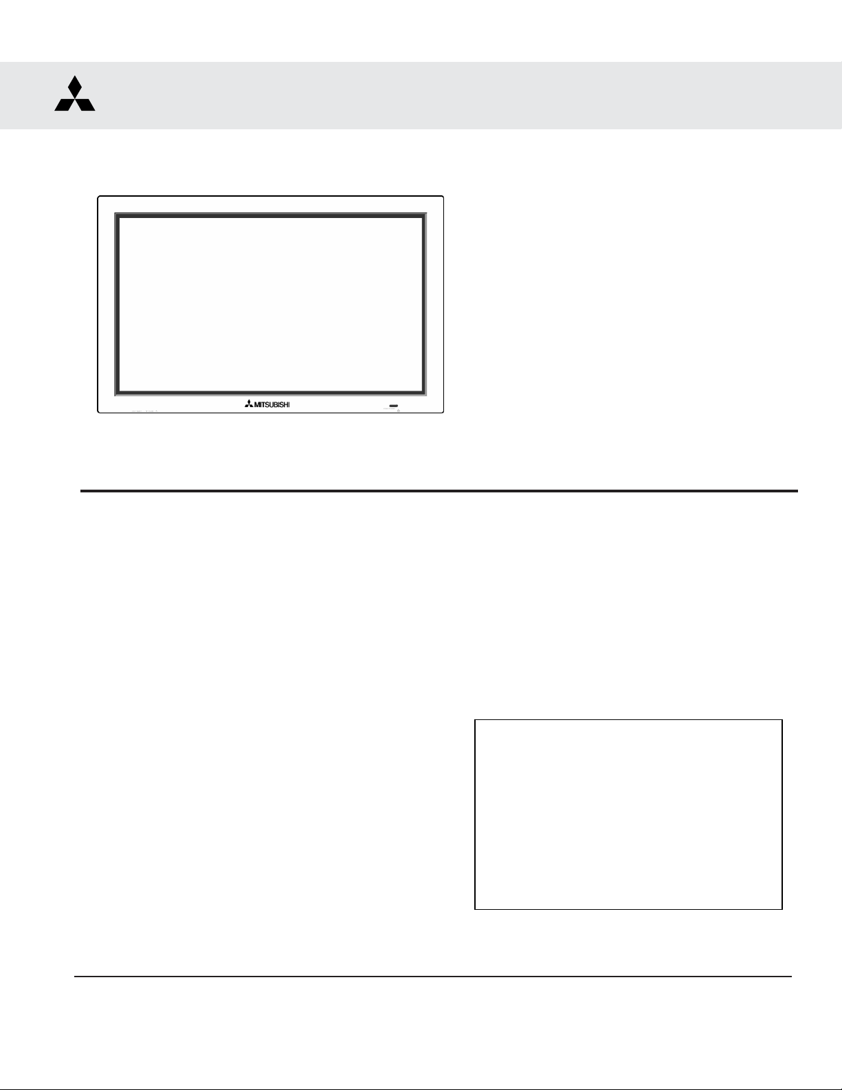
PD-5050
CAUTION:
Before servicing this chassis, it is important that the service person read the "SERVICE SAFETY" section in this
manual.
SPECIFICATIONS
• Power : AC 120V, 50/60Hz
480W (Typical)
6.4A (Maximum)
• Signals
Sync Range : Horiz : 15.5 to 110kHz
(Automatic : step scan)
: Vert : 50.0 to 120 Hz
(Automatic : step scan)
Input Signals : RGB, HD*
DVD*
• Input Terminals
RGB : Visual 1 (Analog) : Mini D-sub 15-pin
Visual 2 (Analog) : BNC (R,G,B,H/CS,V)*
Visual 3 (M-LINK) : MONITORLINK
Video : Visual 1 : BNC
Visual 2 : RCA-pin
Visual 3 : S-Video: DIN 4-pin
DVD/HD/DTV : Visual 1 : RCA-pin (Y,PB[CB},PR{CR])*
Visual 2 : BNC (Y,PB[CB},PR{CR])*1 *
Visual 3 (M-LINK) : MONITORLINK
Audio : Stereo RCA x 3 (Selectable)
External Control : D-sub 9-pin MONITORLINK
1
, DTV*
1
,
1
TM
(RS232C)
TM
(HDMI)
2
TM
(HDMI)
1
• Sound Output : 9W+9W at 6 ohms
• Dimensions : (W)48.1" (H)30" (D)3.8"
(W)1222 (H)736 (D)96 mm
• Weight : 98 lbs / 44.5 kg
*1
HD/DVD/DTV Input Signals supported:
480P (60Hz) 480I (60Hz)
2
525P (60Hz) 525I (60Hz)
576P (50Hz) 576I (50Hz)
625P (50Hz) 625I (50Hz)
720P (60Hz) 1035I (60Hz)
1080I (50Hz) 1080I (60Hz)
*2
The 5-BNC connectors are used as
RGB/PC2 and HD/DVD2 input.
Select one of them under "BNC SELECT".
• Weight and dimensions shown are approximate.
• Design specifications are subject to change without notice.
MITSUBISHI DIGITAL ELECTRONICS AMERICA, INC.
9351 Jeronimo Road, Irvine, CA 92618-1904
Copyright © 2004 Mitsubishi Digital Electronics America, Inc.
All Rights Reserved
Page 2

Page 3

1-1
CONTENTS
SERVICE SAFETY..................................................................................................................... 2-1
TROUBLESHOOTING ............................................................................................................... 3-1
METHOD OF ADJUSTMENTS .................................................................................................. 4-1
METHOD OF DISASSEMBLY ................................................................................................... 5-1
PARTS LIST ............................................................................................................................... 6-1
CONNECTION DIAGRAM ........................................................................................................ 7-1
CONNECTOR PIN EXPLANATION .......................................................................................... 8-1
BLOCK DIAGRAM ..................................................................................................................... 9-1
Page 4

1-2
Page 5
■Safety cautions
SERVICE SAFETY
2-1
The matters to be observed without fail are explained below. These matters are indispensable for the
prevention of an accident during the maintenance servicing, the “security of products” after the completion of
servicing work, and the “prevention of the repeated occurrence of similar fault.”
(1) The degree of danger and material damage, caused as a result of wrong use by disregarding the contents
of the display” is distinguished and explained in the table below.
WARNING
CAUTION
(2) Kinds of the matters to be observed are classified and explained in the icons shown below.
This icon indicates a dangerous place where an electric shock is anticipated.
This icon indicates the contents of “caution” that must be borne in mind, without fail.
This icon indicates the contents of “caution” that must be practiced, without fail.
If this display is disregarded and equipment is handled
wrongly, this can be a cause of physical injury and a
fire, thus leading a person to death or serious injury.
If this display is disregarded and equipment is
handled wrongly, this may lead to personal injury or
material damage.
WARNING
• Observe the caution matter, without fail.
• Be careful of an electric shock or a burn.
• Modification of equipment is absolutely prohibited. Use the specified parts at all times.
• The replaced parts and wiring must be arranged in the original conditions.
• In the place where a particular caution is needed during maintenance servicing, such a
caution note is displayed with a label or a stamp that is given to the cabinet, chassis,
PWB, etc. These caution notes and also the caution matters of
the instruction manuals, etc., must be observed, without fail.
• The power block or the PDP module involves the sections where high voltage or high
temperature is prevalent. When equipment is energized, use working gloves in order to
prevent an electric shock or a burn. At the time of transportation, disassembly,
reassembly, and the replacement of parts, such a servicing job must be done after pulling
out the power plug.
• If any modification is performed, the validity of the manufacturer’s warranty is lost at that
moment. The personnel who did this modification is responsible for the physical injury or
the like, if it should occur as a result of the modification. The parts used are given the
safety-based characteristics, such as non-flammability or sufficient withstand voltage. The
parts to be replaced shall be those which are specified in the list of replacement
parts.(Example: The lithium battery (circuit symbol BA9501 in the MAIN PWB) will give
rise to explosion if its polarity is wrongly treated.
• For safety reasons, insulation materials like tubes and tapes may be used or some parts
may be mounted clear of the PWB. The internal wiring and the fastening with the
clampers for separation from high-heat and high-voltage parts shall be returned to their
original conditions, without fail.
given in
WARNING
Page 6
2-2
• For the maintenance servicing, safety inspection is needed in accordance with the check list.
• Inspection should be carried out according to the check list shown below, in regard to
safety inspection before and after repairing, authentic repair, and explanation to the
user.
(Method of insulation check)
Mount a PDP module on the product to complete it. After the completion of aging and
others, pull out the power plug from the wall outlet, remove the cable, and turn on the
power switch. Use a 500V megger (Note 1) and confirm that the insulation resistance is
50M. or more between each terminal (except for the 3-core earth terminal) of the power
plug (Note 2) and the external exposed metallic parts (Note 3). If the insulation
resistance is found to be below the specified value, recover the faulty section and make
another insulation check again.
(Note 1) If a 500V megger is not available at that time, use a circuit tester or the like.
(Note 2) In the case of a 3-core terminal, the earth resistance shall be 1Ω or less
between the earth terminal and the earth side of each input terminal.
(Note 3) Head phone jack, speaker terminals, remote control terminals, each I/O
terminals, control terminals, screws, etc.
Check item Check column
Is there any influence by high temperatures (due to direct sunlight, etc.), moisture (steam, etc.), oil
fume, dust, and dew condensation?
Is the condition of ventilation acceptable (distance to the wall, ventilation holes, etc.)?
Is the condition of the antenna acceptable (reach to the wire, bend, tilt, etc.)?
conditions
Is the condition of power supply acceptable (regular outlet, adequate earthing, concentrated wiring, etc.)?
Installation
repairing
Safety inspection before
Authentic repair
Safety inspection after repairing
Explanation to the user
Is the condition of installation acceptable (unstability, height, tilt, falling preventive materials, etc.)?
Are the power plug and the power cord free from damage or the attachment of dust?
Is the product free from unusual sound, unusual odor, or unusually high temperature?
Are the knobs, handles, and back cabinet free from abnormality (rattling, drop off, etc)?
Product
Is equipment free from any abnormality in daily use?
main body
Is the symptom examined according to the user’s statement?
Is the product disassembled to the grade where troubleshooting is possible?
Is the symptom reproduced, the faulty part located as a result of fault diagnosis, and replaced?
Trouble-
shooting
Is the normal condition confirmed after aging?
Is the part, specified in the list of parts, used for the power unit?
Is the part, specified in the list of parts, used for the insulation material (material, thickness, etc)?
Is the part, specified in the list of parts, used for the power plug and the power cord?
Is the part, specified in the list of parts, used for the internal cabling and the high voltage lead wires?
Is the part, specified in the list of parts, used for the PDP module?
Specified parts
Are the rest of replaced parts those specified in the list of parts?
Is the part version correct?
Are the part mounting position, fixing method, and the distance the same as those of original?
Is the wiring layout the same as the original (connector, clamper , distance from a heat generating part, etc)?
Is the soldering condition acceptable (whisker, too much solder, tunnel, failure in winding, etc)?
Wires
mounted
Is the insulation material the same as the original (tubes, tapes, fiber, etc.)?
Are the repaired section and its peripheral parts free from abnormality?
Is there any intrusion of foreign substances (solder chips, wire chips, screw chips, screws, etc.)?
Is everything free from danger due to deterioration (discoloration, damage, leakage, etc.)?
Is the safety protection circuit in normal operation?
Are contamination and dust removed after final finish?
Is there any failure in mounting and tightening (back cabinet, falling preventive materials, etc.)?
Is there any influence by high temperatures (direct sunlight, stove, etc.), moisture (steam, etc.), oil fume,
dust, and dew condensation?
Is the condition of ventilation acceptable (distance to the wall, ventilation holes, etc.)?
Is the condition of the antenna acceptable (reach to the wire, bend, tilt, etc.)?
Is the condition of power supply acceptable (regular outlet, adequate earthing, concentrated wiring, etc.)?
Is the condition of installation acceptable (unstability, height, tilt, falling preventive materials, etc.)?
Is the insulation check finished with a circuit tester or the like? (Refer to the above description, “Method of
insulation check.”)
Are the contents and actual treatment of repairing and safety inspection services duly explained?
To use equipment after reading through the instruction manual.
Not to dislodge the back cabinet.
Not to insert anything in ventilation holes and clearances.
To pull out the power plug if the product is not used for a long time.
To ask an NEC’s authorized maintenance service company for the cleaning of the product interior
for the removal of dust.
To turn off the power switch when cleaning the panel surface and the cabinet.
Explanation of use
To turn off the power switch of the main unit for the product provided with a remote control, in case
of going out or sleeping.
Are explanations given to pull out the power plug in case of abnormality and to contact the dealer or an
NEC’s authorized maintenance service company.
Page 7
2-3
CAUTION
• Observe the caution matter, without fail
• The caution matters of
observed, without fail.
given in the instruction manuals, etc., must be
CAUTION
• Do not give shocks and vibration.
• The panel surface (display plane) of the filter and the PDP module is made of glass. If
any shocks or vibration is applied, it may be broken and the scattered glass chips will
be a cause of injury.
• Do not put anything.
• Do not put anything on the product. Otherwise, this can be a cause of injury as a result
of falling down or dropping caused by imbalance.
• Transportation must be done by enough personnel.
• The product is heavy. In the case of transportation, unpacking, or packing, more than
two persons should do it (four persons for a product of 50-inch or larger) by supporting
the top and the bottom of the product.
■Miscellaneous caution matters
(1) This product uses highly integrated semiconductor parts. Since these parts are fragile to
electrostatic charges, earth bands should be used for handling. The product should be handled
where measures have been taken against electrostatic charges.
(2) For this product, the PDP modules and the PWBs are repaired by replacement in a unit.
Therefore, the units of the PDP modules and the PWBs must not be repaired or disassembled.
Otherwise, the validity of warranty will be lost.
(3) If this product is used for the fixed character display or the like as in the case of a character
display board, a phenomenon of burning (not warranted) will occur. Burning is a phenomenon
that the unevenness in the brightness is caused in the display. In such a case, the brightness in
the section where the integrated display time is longer becomes lower than the brightness in
another section where the integrated display time is shorter. This phenomenon is in proportion
to the integrated display time and the brightness. For this reason, to relieve this difficulty during
servicing, do not use any still picture, but use a display by motion pictures of a video or the like.
In addition, use “FULL” for the screen mode and avoid using any display by “NORMAL”,
“TRUE”, or MULTI SCREEN like side by side etc. If it is necessary to use only a still picture for
unavoidable reasons, use a burning relief function such as “PLE LOCK”, “ORBITER”,
“SCREEN WIPER”, etc.
(4) When a PDP module is operated after a long time of storage, it may encounter a difficulty like a
failure in displaying a screen or unstability according to the condition of storage. In such a case,
the PDP module should be incorporated in the product and aging treatment should be carried
out for about two hours (all screen display).
(5) Sulfides will deteriorate the PDP module and this is a cause of malfunction. Therefore, it is
absolutely prohibited to put any vulcanized rubber or a material containing sulfur in the vicinity
of the PDP module.
(6) When taking out a PDP module from the maintenance package box, do it slowly so that the
Page 8

panel surface does not get any shock or stress.
2-4
(7) If one touches the connector of the flexible cable exposed to the rear side of the PDP module,
there is danger of causing a poor contact. As such, it must be handled with utmost care. In
addition, the flexible cable is very weak in mechanical strength. Therefore, this cable must not
be touched during handling.
(8) The panel surface of the filter and the PDP module is easy to be hurt. These components
should be handled very carefully not to press or rub them with a hard thing. Never put them on
a hard thing with the panel surface faced downwards.
(9) When the panel surface of the PDP module is contaminated, gently wipe off the contaminant
with a piece of soft dry cloth. Liquid-state contamination can be removed by lightly pressing it,
without rubbing it. If it is difficult to remove the contamination, use a piece of cloth soaked with
a neutral detergent. The cloth for wiping off should be clean. Never use the same cloth
repeatedly. If a cleansing detergent or water drops should enter the module interior or be
attached to the module surface other than the display plane at the time of cleaning, this will
give rise to the destruction of the product when the product is energized.
(10) Refer to the “Instruction Manual” in regard to contamination in the filter and the cabinet.
(11) When transporting this product, use the packing materials specified in the list of parts. Once
used, such packing materials should not be used again.
(12) This product is composed of a variety of parts, such as those made of materials like glass,
metal, plastics, etc., and those like a lithium battery (circuit symbol of the MAIN PWB: BA9501),
etc. Therefore, when abandoning this product, this should be done in accordance with the
relevant law of the nation or an autonomous body.
CAUTION: Risk of Explosion if Battery is replaced by an Incorrect Type. Dispose of Used
Batteries According to above the Instructions.
Page 9

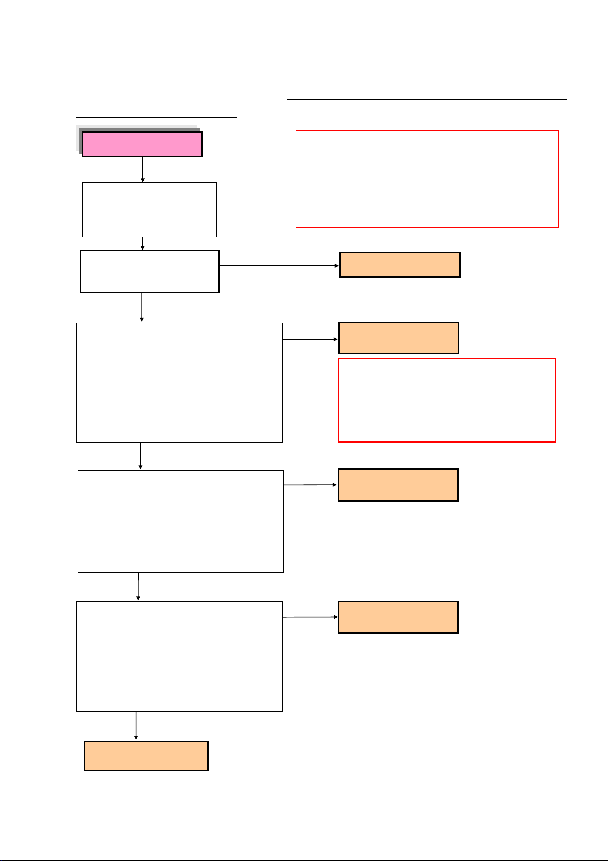
TROUBLESHOOTING CONTENTS
Power Supply does not switch ON
LED does not light. ................................................................................................................. page 3-2
LED blinking green (2 sec. intervals), temperature sensor alarn .............................................. page 3-3
LED blinking green (0.5 sec. intervals), fan error alarm ............................................................ page 3-4
LED blinking red, temperature error alarm ................................................................................ page3-5
LED alternate red/green blinking, PDP error alarm ................................................................. page 3-6
LED comes on gree then goes red, power voltage error alarm ................................................. page 3-7
Image Defects
Image burn .............................................................................................................................. page 3-8
Loss in brightness .................................................................................................................. page 3-8
Failure in writing...................................................................................................................... page 3-8
Pixel Defects .......................................................................................................................... page 3-9
Wron lighting ........................................................................................................................ page 3-10
Dark images1 ....................................................................................................................... page 3-10
Horizxontal lines ................................................................................................................... page 3-10
Block defects ........................................................................................................................ page 3-12
No picture ............................................................................................................................. page 3-14
Audio Problems ................................................................................................................................ page 3-15
Remote Problems
Wired Remote not effective ................................................................................................... page 3-16
Wireless Remote not effective ............................................................................................... page 3-17
Page 3-1
Page 10
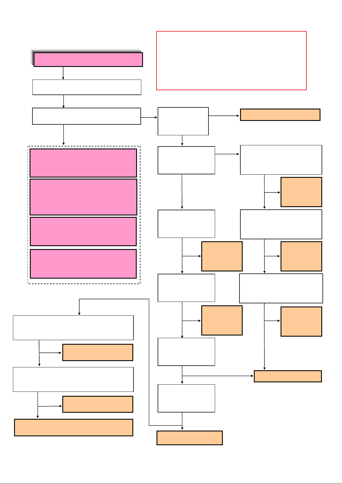
1. Power failure
3-2
(1) The power supply is not turned on.
Move the main power setting for
OFF→ ON.
Is the POWER/STANDBY lamp lit?
(2) Blinking in green (Alarm of
temperature sensor error or fan error)
Go to (P3-3)
(3) Blinking in red after repeating
reciprocal flash in red and green
(POWER ON↔OFF) 3times (Alarm of
temperature error) Go to (P3-5).
(4) Reciprocal flashing in red and
green (Alarm of panel error) Go to
(P3-6).
(5) Lighting in green, and then in
red (Alarm of power line error) Go to
(P3-7).
Is a 5Vdc output available in the state that
the LD connector is disconnected and the
main power is turned ON?
YES
NO
Is a 5Vdc output available in the state that
the RS connector is disconnected and the
main power is turned ON?
YES
NO
The PW connector, PWR PWB or the MAIN
PWB is fault.
YES
The LD connector or the
LED PWB is fault.
The RS connector or the
232C PWB is fault.
(Caution) If any abnormality is sensed in such a
NO
Is the AC power
output available at
the AC connector
(power cord)?
YES
Is a 6.8Vdc output
available at Pin of
the PM connector?
YES
Is a 6.8Vdc output
available at Pin of
the PW connector?
YES
Is a 6.8Vdc output
available at Pin of
the PM connector?
YES
Is a 4.9Vdc output
available at Pin of
the PM connector?
NO
Is a 5Vdc output
available at Pin of
the PW connector?
NO NO NO
The MAIN PWB is fault.
manner that the LED flashes or lights, all
the power lines other than those of 7Vdc
(M+7V) and 5Vdc (M+5V) are automatically
turned off in about 10 seconds. When
checking the power lines other than those of
M+7V and M+5V, a circuit tester or the like
should have been connected in advance.
NO
The PW
connector or
the PWR PWB
is fault.
NO
The PM
connector or
the MAIN
PWB is fault.
NO
NO
The power cord is defective.
Is a 6.8Vdc output available in
the state that the LD connector
is disconnected and the main
power is turned ON?
The LD
YES
connector or
the LED PWB
NO
Is a 6.8Vdc output available in
the state that the PW connector
is disconnected and the main
power is turned ON?
NO
Is a 6.8Vdc output available in
the state that the PM connector
is disconnected and the main
power is turned ON?
is fault.
The PW
YES
connector or
the PWR PWB
is fault.
YES
The PM
connector or
the MAIN
PWB is fault.
NO
YES
The power unit is fault.
YES
Page 11
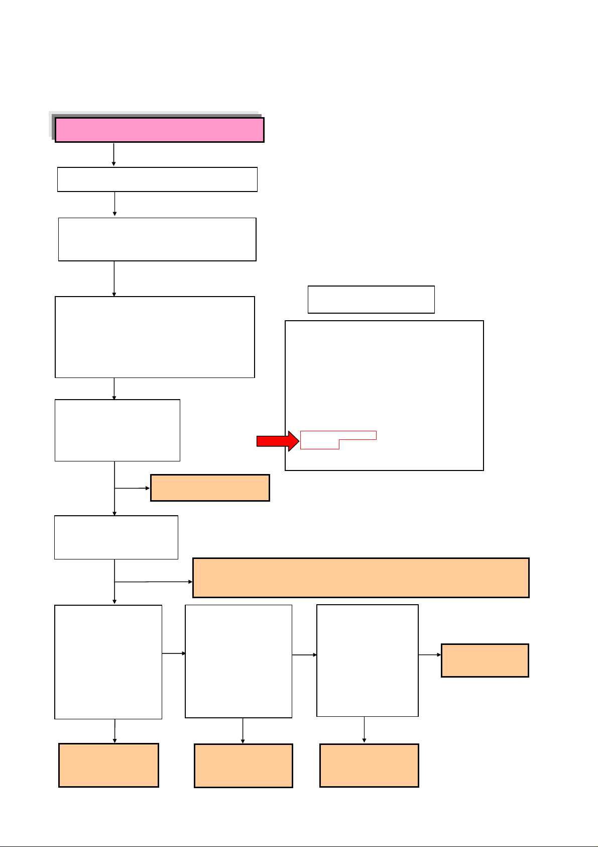
(2) Blinking in green
3-3
Alarm of te mperature sensor error
Blinking in green (intervals of 2 seconds)
Turn off the main power supply.
Pressing the [MENU] key of the product,
turn on the main power supply to cancel
alarming.
Press the remote control keys in the
order of [MENU] [MUTE] [EXIT] [SLEEP]
[EXIT] and enter the diagnostics menu.
Press the [MENU/ENTER] key to
display the FAN SET menu (P2/11).
Is there a display of
numerals (almost room
temperatures) at the right
side of [T1, T2, T3]?
YES
The MAIN PWB is fault.
NO
FAN SET
FAN SET
FAN MODE H CONT ENA –
FAN OFF/L – CONT UP –
FAN L/M – CONT TIME –
FAN M/H – UP STEP 2
SF SAVE 075 DOWN STEP 2
PLE SAVE 070 READ TIME 60
T ALM 095 TEMP LEVEL 1
RET TME 030
PLE TIME 001
T1 030 T2 025
T3 030 T4 – MODE 2
IC ERROR –
[MENU/ENTER] NEXT [EXIT] PREV 2/11
Is there a display of [-] for
all the numerals at the
right side of [T1, T2, T3]?
YES
Are there a 3.3Vdc
output at Pin and a
clock signal (3.3Vpp)
at Pins and of the
TS in the state that the
TS connector is
disconnected and the
main power supply is
turned on?
NO
NO
The TS connector
YES
or the SENC PWB
is fault.
When a [-] display is presented, the PWB with the symbol shown
below is fault. T1: SEND PWB, T2: SENB PWB, T3: SENC PWB
Are there a 3.3Vdc
output at Pin and a
clock signal (3.3Vpp)
at Pins and of the
TR in the state that the
TR connector is
disconnected and the
main power supply is
turned on?
YES
The TR connector
or the SEND PWB
is fault.
Are there a 3.3Vdc
output at Pin and a
NO
clock signal (3.3Vpp)
at Pins and of
the TM in the state
that the TM connector
is disconnected and
the main power
supply is turned on?
The TM connector
or the SENB PWB
is fault.
YES
NO
The MAIN PWB
is fault.
Page 12
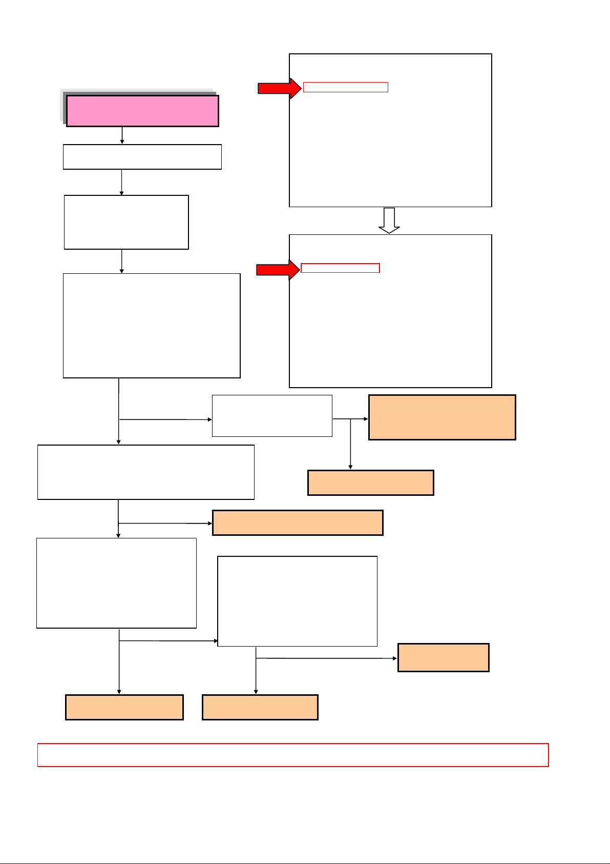
Alarm of fan error
3-4
Blinking in green (intervals of
0.5seconds)
Turn off the main power supply.
Pressing the [MENU] key
of the product, turn on the
main power supply to
cancel alarming.
Is the fan running?
(Caution) When alarming is
canceled, [FAN MODE] of
FAN SET (P2/11) in the
diagnostics menu
automatically moves from
[ENA] to [H], thus causing
the fan to run.
FAN SET
FAN MODE ENA CONT ENA –
FAN OFF/L – CONT UP –
FAN L/M – CONT TIME –
FAN M/H – UP STEP 2
FAN SAVE 075 DOWN STEP 2
PLE SAVE 070 READ TIME 60
T ALM 095 TEMP LEVEL 1
RET TME 030
PLE TIME 001
T1 030 T2 025
T3 030 T4 – MODE 2
IC ERROR –
[MENU/ENTER] NEXT [EXIT] PREV 2/11
FAN SET
FAN MODE H CONT ENA –
FAN OFF/L – CONT UP –
FAN L/M – CONT TIME –
FAN M/H – UP STEP 2
FAN SAVE 075 DOWN STEP 2
PLE SAVE 070 READ TIME 60
T ALM 095 TEMP LEVEL 1
RET TME 030
PLE TIME 001
T1 030 T2 025
T3 030 T4 – MODE 2
IC ERROR –
[MENU/ENTER] NEXT [EXIT] PREV 2/11
YES
NO
Is there a 3.3Vdc output
at Pin of the FA and
FB, connectors?
Is there a voltage output of 11.2Vdc
at Pin 1 of the FA, FB, and FC connectors?
NO
YES
The FAN-A/FAN-B is fault.
Is there a voltage output of
11.2Vdc when the FA
connector is disconnected and the
main power is turned ON?
YES
NO
Is there a voltage output of
11.2Vdc when the FB
connector is disconnected and the
main power is turned ON?
YES
The FAN-A is fault.
The FAN-B is fault.
YES
The fan is out of order on the
side where a 3.3Vdc output
is generated.
NO
The MAIN PWB is fault.
NO
The MAIN PWB
is fault.
(Caution) In the FAN MODE, [ENA] is automatically recovered when the main power is turned OFF → ON.
Page 13

(3) Blinking in red (Alarm of temperature error)
3-5
Since the internal temperature is too high in the product, the temperature protector has been actuated. In such
a case, the following actions should be taken immediately:
1. Turn off the main power supply and pull out the power cord from the wall outlet.
2. Wait for about 60 minutes until the temperature in the main unit lowers.
3. Check whether the heat discharge port is covered with dust or the like. If yes, remove the clogging substance.
4. If the unit is used where the ambient temperature is high, it should be moved to an adequate place (air
temperature ranging from 5°C to 35°C).
Page 14
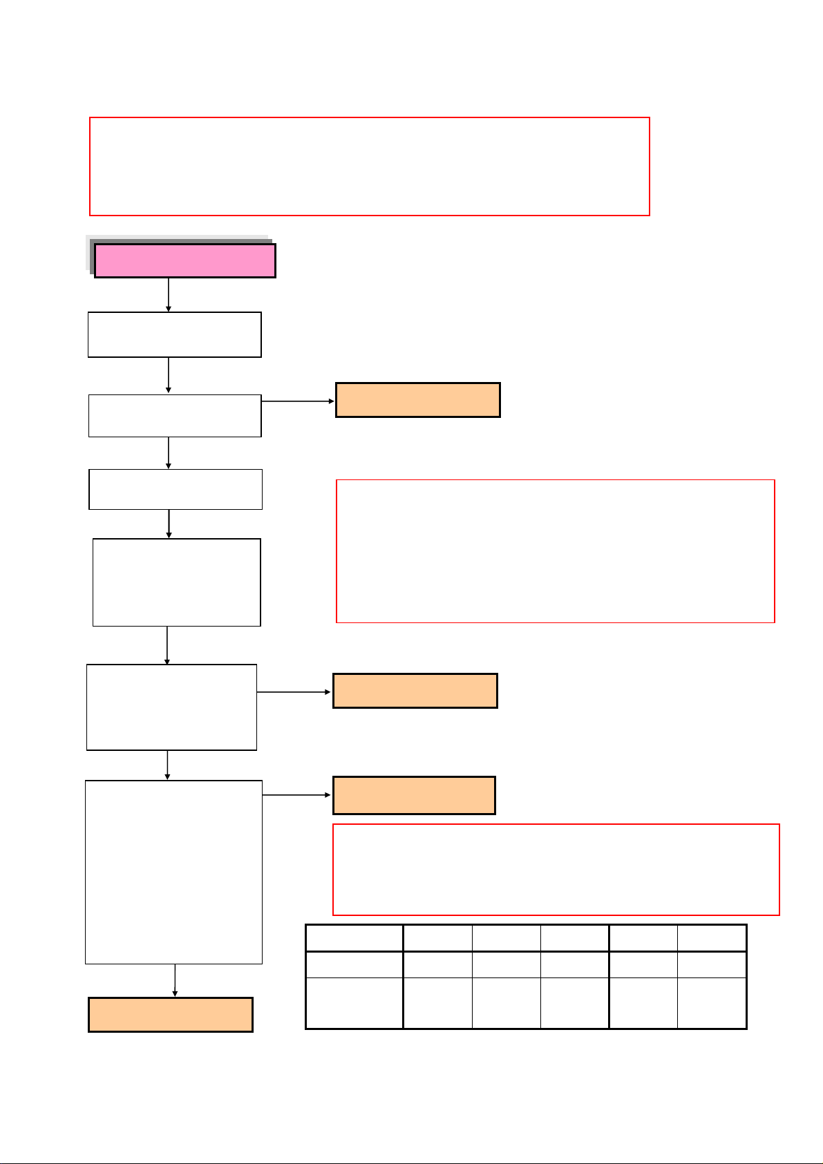
(4) Alternation blinking in red and green (Alarm of PDP error)
3-6
(Caution) How to reset the alarming condition
Blinking in red and green
Move the main power
setting for OFF → ON.
Is there alternation blinking
in red and green?
Turn OFF the main power
supply.
With the [Menu] key of the
product kept pressed, turn
on the main power supply
to assume the [Voltage
Check Mode].
Pressing the [Input Select] key of the product, turn on the main power supply
of the main unit. In this state, keep pressing the [Input Select] key for more
than 2 seconds until alarming is canceled. Make confirmation by the method
specified below.
NO
Normal
YES
(Caution) When the main power supply is turned on with the
[Menu] key of the product kept pressed, it takes 30
seconds more to assume the state of [blinking in red and
green]. In this time period, the following voltage checks
should be carried out.
If the state of [blinking in red and green] is assumed
during this checking, take actions of [Alarm Canceling]
and [Voltage Check Mode Setup] again.
Is there a 3.3Vdc output at
Pin 94 of IC9501 in the
MAIN PWB? (See the
PWB Layout Diagram on
P4-20.)
Turn ON the main power
supply in the state that the
AD, PD, and PH connectors
are disconnected. In this
state, are there the outputs
of Vs (170Vdc), Vd (60Vdc),
and 5Vdc at the PD/PH
connectors as specified in
the table at right? In this
case, however, no images
are generated.
NO
YES
The PDP is fault.
YES
NO
The MAIN PWB is fault.
The Power unit is fault.
(Caution) The voltage values of Vd and Vs and also the connector
pin numbers can differ according to the PDP. The method
of checking these voltage values is obtainable from [2.
Adjustment of the power unit] in the method of adjustment
plus the table specified below.
Inch Vs Vd GND 5Vdc GND
50 PD-9pin PD-7pin PD-5pin PH-1pin PH-3pin
61
PD-9pin
PH-1pin
PD-7pin
PH-4pin
PD-5pin
PH-5pin
PD-4pin
PH-7pin
PD-5pin
PH-5pin
Page 15
(5) Lighting in green, and then in red (Alarm of power voltage error)
3-7
Unlike [lighting in red] in the STANDBY mode, [lighting in green] continues for about 30 seconds without any
output of images and audio signals. Since then, the mode turns into [lighting in red].
Lighting in red
Make an OFF → ON setting
twice for the main power
supply in order to reset the
alarming condition.
Is the LED lit in red after it
has been lit in green for about
30 seconds?
YES
When the main power supply is turned on in
the state that the AD, PD, and PH
connectors are disconnected, are there the
Vs (170Vdc) and Vd (60Vdc) outputs at Pins
- to Pins - of the PD connector and
a 5Vdc output at Pins - of the PH
connector? In this case, is the LED not
turned in red after it has been lit in green for
about 30 seconds? At that time, however, no
ima
ges are generated.
NO
When the main power supply is turned on in
the state that the PA and PV connectors are
disconnected from one after another, is
there a 12Vdc output at Pins - of the PA
connector or the 12Vdc and 6Vdc outputs at
Pins and - of the PV connector? In
this case, is the LED not turned in red after it
has been lit in green for about 30 seconds?
NO
(Caution) How to reset the alarming condition The
alarming condition can be reset when an
OFF→ ON setting is repeated twice for the
main power supply in the state that the
LED is lit in red. The interval between the
first and second settings is not particularly
specified.
Normal
YES
YES
The PDP is fault.
(Caution) The voltage values of Vd and Vs
can differ according to the PDP.
The method of checking these
voltage values is obtainable from
[2. Adjustment of the power unit]
in the method of adjustment.
The MAIN PWB or the
AUDIO PWB is fault.
Is there an output of 3.3Vdc available at Pins
~ and 2.5Vdc at Pins ~ in the
state that the PA and PV connectors are
returned to the former state, the main power
is turned ON, and the PN connector is
disconnected? In this case, however, this
check must be finished in 30 seconds.
Otherwise, there will be power tripping on
account of an alarm.
NO
YES
The MAIN PWB is fault.
NO
The Power unit or the
PN connector is fault.
Page 16
3-8
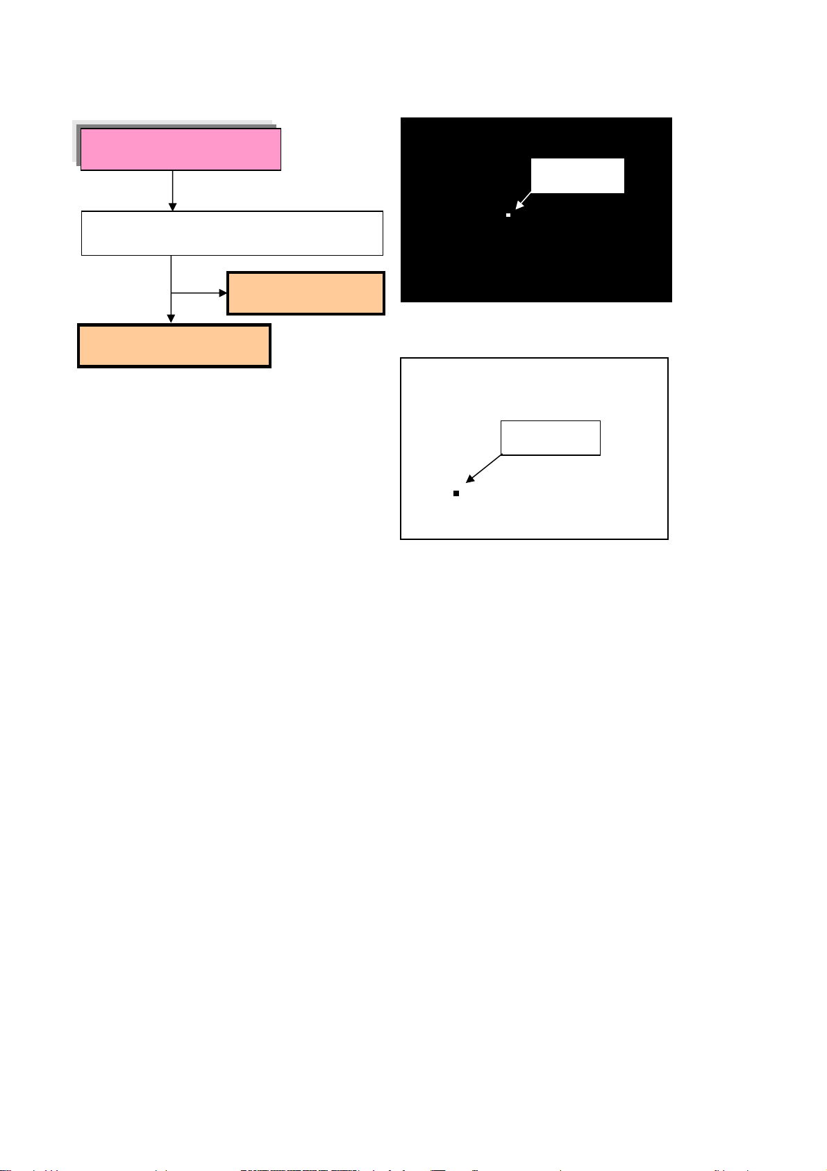
2. Image errors
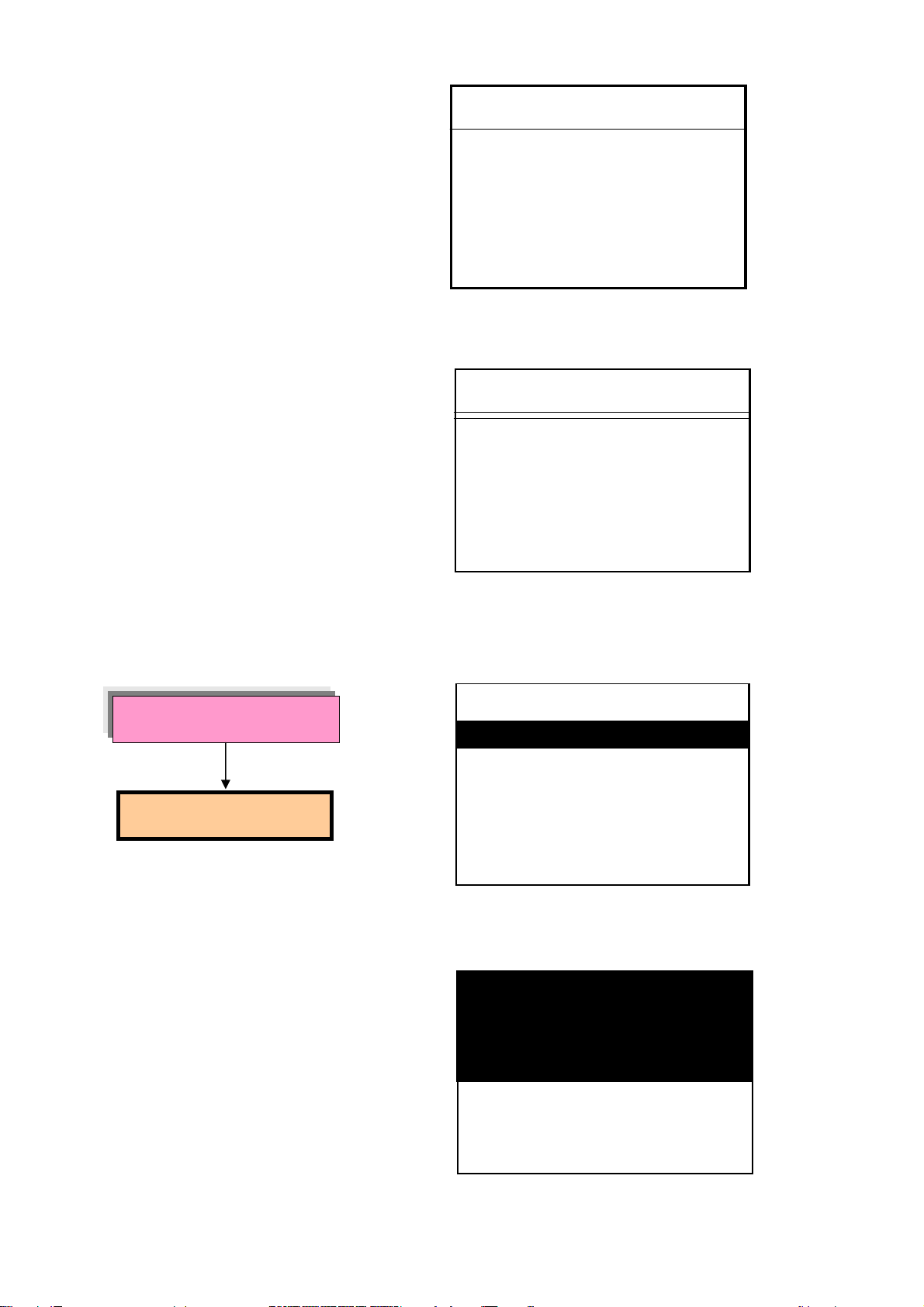
(Caution) Typical abnormal images are shown below. All errors do not always fall on these error samples.
(1) Image burn and deterioration in brigh
Residual images are seen
without signal entry.
(2) Failure in writing
(To the separate PDP service manual)
This is not a fault.
Deterioration in brightness
This is not a fault.
Failure in writing
The PDP is fault.
tness
A
No signal
All-whitesignal
All-whitesignal
Dot errors change
with no continuity.
All-whitesignal
Page 17
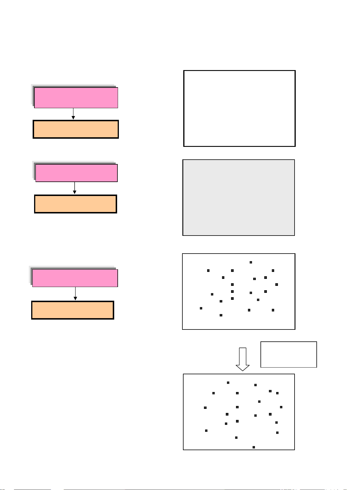
(3) Pixel defect
3-9
Pixel defect
Are there many defective pixels exceeding the
pixel defect standard?
NO
This is not a problem.
YES
The PDP is fault.
[Pixel defect standard for reference]
Bright defect
(Fig. 1) All-Black Signal
Dark defect
(Fig. 2) All-White Signal
Page 18
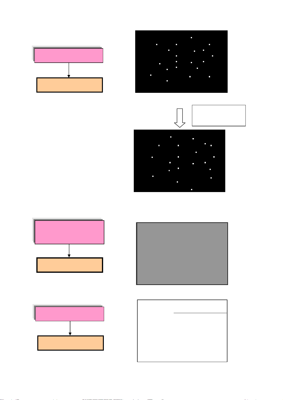
(4) Wrong lighting
3-10
Wrong lighting
The PDP is fault.
(To the separate PDP service manual)
All-black signal
Dot errors change
with no continuity.
All-black signal
(5) Dark images [Other than the deterioration in brightness as per (1) above]
The images are dark even
with an all-white input
The PDP is fault.
(To the separate PDP service manual)
(6) Defect in horizontal lines
Line defect
The PDP is fault.
(To the separate PDP service manual)
All-white signal
All-white signal
Page 19
3-11
Defect in the block unit
All-white signal
All-white signal
The PDP is fault.
All-white signal
All-white signal
Page 20
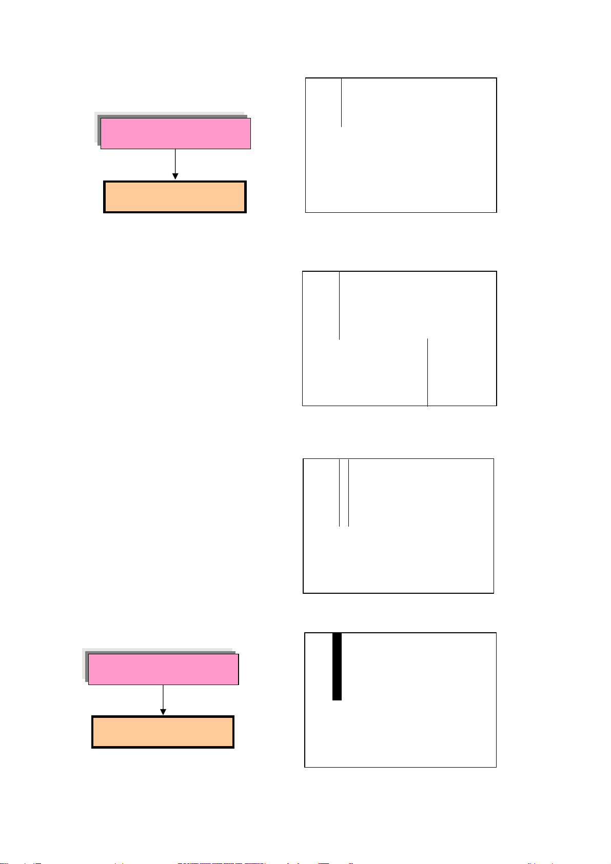
(7) Defect in vertical lines
3-12
Defect in vertical lines
The PDP is fault.
All-white signal
All-white signal
All-white signal
Block defect
The PDP is fault.
All-white signal
Page 21

3-13
All-white signal
All-white signal
Page 22
(8) No pictures [(Caution) The voltage outputs of Vs = 170V and Vd = 64V, 5Vdc are always generated, but the
3-14
LED is not flashing or lighting for alarming. However, the voltage values can differ according to the PDP.]
No picture is displayed.
Make the setting of OFF→ ON
for the main power supply.
Does the priming glimpse?
YES
When the AD connector is disconnected, is
the LVDS signal normally output to each
pin of the AD connector? (For more details
of the signal, refer to the descriptions about
the connector pins.)
NO
YES
The PDP is fault.
NO
The MAIN PWB is fault.
The AD connector or the PDP is fault.
Page 23

3. Audio errors
3-15
(Caution) In regard to the method of audio input setting, refer to the specifications and the instruction
manual to confirm that all the setting is free from errors. Since then, troubleshooting can be
carried out. It must be noted that the protector functions and no audio output is available if
the opposing electrodes of the speaker output or the speaker output and the ground (GND)
are short-circuited. In such a case, turn off the main power supply and make the
connections correctly. The protector is reset when the main power supply is turned on after
Audio errors
In the state that the speaker cable is
disconnected, is the audio signal output
available at the speaker terminal?
Is the voltage output specified below
NO
available at each pin of the PA connector
in the AUDIO PWB?
Pin_NO Name Voltage
1 S+12 12Vdc
2 S+12 12Vdc
3 S+12 12Vdc
4 GND GND
5 GND GND
6 GND GND
YES
Is the waveform specified below output to
the AU connector of the AUDIO PWB?
Pin6
Pin7
Pin5
Pin 1,3 • • • Audio signal waveform
5Vpp
5Vpp
3.5Vdc
YES
NO
NO
The speaker or the speaker
cable is fault.
The power unit or the PA
connector is fault.
The MAIN PWB or the AU
connector is fault.
The AUDIO PWB is fault.
YES
Page 24

4. Remote control not effective
p
3-16
(1) The wired remote control is not effective.
When a single item is used
The wired remote control is not
effective.
Is there a signal output specified below
at Pin 7 of the RS connector?
3.3Vpp
Is there a signal output specified below
at Pin 3 of the M2003? (Refer to the
PWB layout diagram on Page P4-21.)
NO
5Vpp
When the RS connector is
disconnected, is there a signal output
specified below at the RS connector of
the
MAIN PWB?
Pin No. Pin name Voltage
1 M+5V 5Vdc
5 M+3.3V 3.3Vdc
YES
(Caution) The wired remote control is not effective if the setting
of [PLE LINK], or [Repeat TIMER] is ON, or if the
setting of [ID NUMBER] has been made. Therefore,
such a setting should be turned off, without fail. Since
then, troubleshooting can be carried out.
YES
NO
The RS connector or the
MAIN PWB is fault.
Is there a 3.3Vdc output
at Pin 2 of the M2003?
(Refer to the PWB layout
diagram on Page P4-21.)
YES
The remote control or the
remote control cable is fault.
NO
The RS232C PWB is fault.
NO
The RS connector or the
MAIN PWB is fault.
YES
The 232C PWB is fault.
When a daisy chain (including the video wall) is used
The wired remote control
is not effective.
Are the 0Vdc and 5Vdc
outputs respectively available
at Pins 9 and 10 of the RS
connector in the standard
roduct of 232C PWB?
The MAIN PWB is fault.
NO
Is there a clock signal output at
YES
Pin 3 of the M2004? (Refer to
the PWB layout diagram on
Page P4-21.)
The 232C PWB is fault.
NO
Check the products of
YES
second and thereafter
according to “1 When a
single item is used.”
Page 25

(2) The wireless remote control is not effective.
s fault
3-17
(Caution) Since the detection of “wired” or “wireless” is conducted for the remote control
through the remote terminal, it is necessary to pull out the remote control cable
from the remote terminal, without fail. Troubleshooting should be carried out after
confirming that “IR REMOTE” is set at ON and that “ID NUMBER” is at ALL
according to the user’s menu.
The wireless remote control is not
effective.
Is there a 0Vdc output at Pin 12 of the
RS connector?
YES
Is there a signal output specified
below at Pin 6 of the PW connector?
5Vp-p
NO
Is there a signal output specified
below at Pin 1 of the LD connector?
5Vp-p
The LED connector or the LED PWB is fault.
NO
NO
YES
YES
When the RS connector is disconnected,
is there a 0Vdc output at Pin 12 of the RS
connector in the MAIN PWB?
YES
The 232C PWB or the RS
connector is fault.
NO
The MAIN PWB is fault.
The PW connector or the
PWR PWB i
.
Page 26

Page 27

4-1
METHOD OF ADJUSTMENTS
■Adjusting conditions
Adjustments should be carried out in the procedures of A to D specified below. However, any
adjustments other than the items A to D below are not required.
A. When the “PDP module” is replaced, adjustments should conform to the
adjusting items of [1 and 2] specified below.
B. When the “POWER UNIT” is replaced, adjustments should conform to the
adjusting item of [2] specified below.
C. When the “MAIN PWB” is replaced, adjustments should conform to the
adjusting item of [3] specified below.
D. When the "HIGH VOLTAGE PWB" is replaced, adjustments should conform to
■Adjusting items
1. Clearing of the usage time (Using the remote control)
(1) Press the keys in the order of [MENU] [MUTE] [EXIT] [SLEEP] [EXIT] in order to
enter the diagnostics menu.
(2) Press the [MENU/ENTER] key to select the [USAGE TIME] menu (8/11). Then, the integrated time
[34567 (hours)] (example) accumulated till the present time is displayed when the main power supply
is turned on (except for the standby mode).
the adjusting item of [4] specified below.
USAGE TIME
34567H
232C-ALARM RX 0
T X 0
[MENU/ENTER] NEXT [EXIT] PREV 8/11
(3) When the keys are pressed in the order of [MUTE] → POSITION/CONTROL [ ] →
POSITION/CONTROL [ ] → [SLEEP], the display is cleared to [00000H]. At that time, the
characters of [RESET] are displayed for about 5 seconds on the right side of time display.
USAGE TIME
00000H RESET
232C-ALARM RX 0
T X 0
[MENU/ENTER] NEXT [EXIT] PREV 8/11
Page 28

4-2
2-2. For PD-5050
2-2-1. Adjustment of the Vs voltage
(1) Enter a color bar input by means of either video signal of VIDEO input, or DVD/HD input, or RGB
input, and turn on the power switch of the main unit.
(2) Turn the volume control (RV6) in the power unit and make adjustments until the voltages of CH2 and
CH1 (D, GND) of the power unit attain the voltage values specified for the PDP (Vs value of the
voltage regulation indicator label on below the figure) ±1V.
2-2-2. Adjustment of the Vd voltage
(1) Enter a color bar input by means of either video signal of VIDEO input, or DVD/HD input, or RGB
input, and turn on the power switch of the main unit.
(2) Confirm that the voltages of CH4 and CH1 (D, GND) of the power unit are maintained at the voltage
values specified for the PDP (Vd value of the voltage regulation indicator label on below the figure)
±1V.
Otherwise, turn the volume control (RV5) until the voltage attains the voltage values specified for the
PDP (Vd value of the voltage regulation indicator label on below the figure) ±1V.
2-2-3. Adjustment of the +5V voltage
(1) Display a color bar by means of either video signal of VIDEO input, or DVD/HD input, or RGB input.
(2) Confirm that the voltages of CH3 and CH1 (D, GND) of the power unit are maintained at “5.15 ±
0.1V”. Otherwise, turn the volume control (RV2) until the voltage attains “5.15 ± 0.1V”.
SERIAL NO.
********
Vd= **V
Vs=***V
CODE -01
OR
Vs/Vd/100/185/220 V
555/84.2/782/10204 K
347 W/0 /2 P
(Caution) Rear-side view when the back cover is removed The label is concealed between the MAIN
PWB and PDP. Check it by peeping through the space from above. The label position can
be changed, without notice.
Page 29

* Top view of the power unit for the PD-5050
4-3
P
V
P
M
P
N
Adjustmen
t of 5
RV3
D+3.3 ADJ
V
CH1
D.GND
RV2
D+5 ADJ
CH3
Vcc
RV5
D+70 ADJ
PH
CH4
Vd
RV6
D+170 ADJ
PD
CH2
Vs
Adjustment of
the Vs voltage
Adjustment of
P
A
the Vd voltage
AC
Page 30

4-4
3. Adjustments after the replacement of the MAIN PWB (Using the remote control)
3-1. Product serial No. registration
(1) Press the keys in the order of [MENU] [MUTE] [EXIT] [SLEEP] [EXIT] in order to
enter the diagnostics menu.
(2) Press the [MENU/ENTER] key to select the [MONITOR INFORMATION] No. menu. (Example : PX-
50XR4A)
(3) Press the [FORMAT] key 4 times to display a cursor in the lower column of [SERIAL/NUMBER].
MODEL NAME
: PX-50XR4A
SERIAL/NUMBER
:
SOFT WARE VERSION
: F123
USAGE TIME
: 00000H
T1 025 T2 025
T3 025 T4 - -
[MENU/ENTER] NEXT [EXIT] PREV
MODEL NAME
: PX-50XR4A
SERIAL/NUMBER
:
SOFT WARE VERSION
: F123
USAGE TIME
: 00000H
T1 025 T2 025
T3 025 T4 - -
[MENU/ENTER] NEXT [EXIT] PREV
MONITOR INFORMATION
MONITOR INFORMATION
(Caution 1)
(Caution 2)
(Caution 1) No modification is possible here because this modification is already finished by 3-2.
(Caution 2) No modification is possible here because registration is already finished at the time of
Factory shipment setting (initial setting).
shipment in terms of maintenance parts.
(4) Moving the POSITION/CONTROL keys of [ ] and [ ], select the numerals and characters of
the serial number that is listed in the serial label located on the rear surface of the product. Register
the serial number. (Blank → 0 ~ 9 → A ~ Z)
(5) Moving the POSITION/CONTROL keys of [ ] and [ ], select the next digit by means of a
cursor.
(6) Repeat the processes of (4) and (5) above and register the serial number completely.
Page 31

4-5
• How to read the serial number
Serial No.
················· Year of manufacture (lower one digit of the year)
················· Month of manufacture (January to September = 1 to 9, October = X, November = Y,
················· GS model: 1, Other than GS model: 0
······ Serial numbers of 0001 to 9999. The serial number starts with 0001 in each month of
················· Place of manufacture
················· Control number S→A→M→T→Z→N→K→U→C→W→J→P
(* Arbitrary for the first symbol)
December =Z)
production. There is no duplication or missing of the number in the same month.
(Example) First unit in March 1999
First unit in November 2000
→ 93000019C
→ 0Y000019W
(Example) When entering a serial number of [2900123 9Z]
Move the POSITION/CONTROL keys of [ ] and [ ] to select [2].
MODEL NAME
: PX-50XR4A
SERIAL/NUMBER
: 2
SOFT WARE VERSION
: F123
USAGE TIME
: 00000H
T1 025 T2 025
T3 025 T4 - -
[MENU/ENTER] NEXT [EXIT] PREV
MONITOR INFORMATION
Move the POSITION/CONTROL keys of [ ] and [ ] to select the next digit.
MODEL NAME
: PX-50XR4A
SERIAL/NUMBER
: 2
SOFT WARE VERSION
: F123
USAGE TIME
: 00000H
T1 025 T2 025
T3 025 T4 - -
[MENU/ENTER] NEXT [EXIT] PREV
MONITOR INFORMATION
Page 32

4-6
Repeat the procedures of and above, and enter all inputs of [2900123 9Z] from the left side.
(7) Following the above, setting must be carried out without fail according to “3-2. Factory shipment
setting (Initial setting)”
MODEL NAME
: PX-50XR4A
SERIAL/NUMBER
: 29001230 9Z
SOFT WARE VERSION
: F123
USAGE TIME
: 00000H
T1 025 T2 025
(Caution) Give a one-digit space between the 7th
T3 025 T4 - -
[MENU/ENTER] NEXT [EXIT] PREV
MONITOR INFORMATION
and 8th digits.
3-2.Factory shipment setting (Initial setting)
(1) Press the [MENU/ENTER] ke to select the [FUNCTION] menu.
(2) Move the POSITION/CONTROL keys of [ ] and [ ] to the item of [SHIP]. Then, move the
POSITION/CONTROL keys of [ ] and [ ] to select [DESTINATION ALPHABETS] shown below.
(The asterisks * shown below denote the numerals or the characters.)
J : PX-*****J JW : OEM Specifications for use in Japan
A : PX-*****A AW : OEM Specifications for North America (PD-5050)
G : PX-*****G GW : OEM Specifications for European countries
W : PX-*****W WW : OEM Specifications for zones other than the above
FUNCTION
SCART OFF SAFEL MODE --SHIP A PLE TEST OFF -LIMIT-VD OFF VD2 VLIM 5HZ
LIMIT-PC ON VD2 YCORB -GAMMA MD 12 VD2 YCOREN ON
VOL OFFSET 2 VD2 CORB -FHCRT COMP 3 VD2 COREN ON
ACTVH TIME 2 VD OUT 10
PSC-T OFF ROTATE PTN 1
EXT-PC OFF BLUE GAIN OFF
[MENU/ENTER] NEXT [EXIT] PREV
(3) Press the keys in the order of [MUTE] → POSITION/CONTROL [ ] → POSITION/CONTROL
[ ] → [SLEEP] to make “Factory shipment setting”. When “Factory shipment setting” is
executed, the red characters of [SET] is shown for about 5 seconds on the right side of the
[DESTINATION ALPHABETS]. The setting is finished when these red characters of [SET] go out. In
regard to the factory shipment setting values, refer to the descriptions given below.
Page 33

4-7
FUNCTION
SCART OFF SAFEL MODE--SHIP A SET PLE TEST OFF --
LIMIT-VD OFF VD2 VLIM 5HZ
LIMIT-PC ON VD2 YCORB 1
GAMMA MD 10 VD2 YCOREN ON
VOL OFFSET 2 VD2 CORB 1
FHCRT COMP 3 VD2 COREN ON
ACTVH TIME 2 VD OUT 8
PSC-T OFF ROTATE PTN 1
EXT-PC OFF BLUE GAIN OFF
[MENU/ENTER] NEXT [EXIT] PREV
(4) Press the keys of the remote control in the order of [MENU] [MUTE] [EXIT]
[SLEEP] [EXIT] in order to withdraw from the Factory shipment setting.
[Factory shipment setting values]
1. Initial setting values for the user menu
MENU A
POWER ON/OFF ON
VOLUME 10step
INPUT MODE VIDEO1
WIDE MODE STADIUM
AUTO PICTURE OFF (RGB1~3)
HD SELECT 1080I
LANGUAGE ENGLISH
COLOR SYSTEM AUTO
All items intended to recover the initial values
through the selection of [All Reset] in the user menu
I
2. Field menu initial setup values (applicable in common to all models)
MENU A
SHIP A
PSC-LIMIT OFF
LIMIT-PC ON
U-SCAN OFF
SERVICE
MONITOR
INFORMATION
V-FREQ OT AUTO
V-FREQ VD AUTO
SYNCLEVEL1 TTL
SYNCLEVEL2 TTL
SUB-ORB ON
PIC FREEZE ON
MODEL NAME PD-5050
Initial values
Page 34

4-8
PD-5050: 50-WXGA,
PD-6150: 61-WXGA,
3. Initial setting values for the Factory shipment setting menu The table shown below specifies only the items
that can be changed in the factory adjusting mode. Therefore, any setting values of the items not specified
below cannot be modified.
A
MENU
SHIP A FUNCTION
LIMIT-PC ON
MONITOR
INFORMATION
SERIAL/
NUMBER
- - - -
Page 35

4. Adjustments after the replacement of the High Voltage PWB.
4-1 Condition of Adjustment
(1) After the High Voltage PWB has been replaced, perform the Vsw1, Vsw2, Vp and Vbw adjust-
ments in the order described.
4-2 Voltage Label Check
(1) Prior to adjustment, note the voltage levels recorded on the Voltage Label as shown.
Vbw Vsw1 Vp Vsw2
Label
Location
Example:
Vbw : 120.3
Vsw1 : 219.8
Vp : 222.6
Vsw2 : 217.6
4-3 Vsw1 & Vsw2 Adjustments Note: Measure voltage between the TP and closest Chassis Ground.
(1) Vsw1 - Adjust VR3 so the voltage at TP328 is set to the level specified for Vsw1 on the Voltage
Label +/- 0.5V.
(2) Vsw2 - Adjust VR4 so the voltage at TP310 is set to the level specified for Vsw2 on the Voltage
Label +/- 0.5V.
Vsw1 & Vsw2
Location
Vsw2
Vsw1
VR3
TP328
TP310
VR4
4-9
Page 36

4-4 Vp & Vbw Adjustments Note: Voltage is measured between the TP and closest Chassis Ground.
(1) Vp - Adjust VR1 so the voltage at TP327 is set to the level specified for Vp on the Voltage
Label +/- 0.5V.
(2) Vbw - Adjust VR2 so the voltage at TP329 is set to the level specified for Vbw on the Voltage
Label +/- 0.5V.
Vp & Vbw
Location
Vp
VR1
TP327
Vbw
VR2
TP329
4-10
Page 37

(Caution) 1. Before disassembly, turn power off the main unit and pull out the power plug from the wall outlet.
5-1
METHOD OF DISASSEMBLY
2. Use a screwdriver with a fitting size. Otherwise, the screw threads may be damaged.
3. Reassembly can be carried out in the reverse order for disassembly. Refer to the disassembly procedures and
forward reassembly in the reverse order.
4. The order for taking out the parts (or components) is indicated by the foregoing numeral that is attached to the
name of each part.
5. The wire connector symbol is indicated by two digits of Marking . Read CN- when examining the table of parts.
6. Class A or Class B in the text is applicable to the models specified. CLASS B: PD-5050
1. Outlined method of disassembly
The outlined procedures for the disassembly of the major parts are shown below (disassembled in the direction of ).
In regard to the details of disassembly, cautions, etc., refer to the method of replacement for each part [page indicated in ( )].
SET
(with a STAND)
STAND
(P5-2)
BACK COVER
(P5-3~5-4)
CHASSIS ASSY
(P5-5)
PDP
(P5-6~5-8)
BRACKET FILTER
(P5-9)
FILTER
(P5-9~5-10)
SET
(without a STAND)
* Modification means that the screws are
mounted or removed.
Modifications
of a STAND *
(P5-13)
Modifications of
a BACK COVER *
(P5-14)
BACK COVER
(P5-3)
FRONT PANEL
(P5-12)
BUTTON COVER
(P5-11)
CONTROL BUTTON
(P5-11)
TERMINAL PANEL M SUB ASSY
(P5-15)
TERMINAL PANEL S
(P5-17)
POWER BUTTON COVER
(P5-18)
TERMINAL PANEL B SUB ASSY
(P5-19)
POWER PWB
(P5-21)
SEND PWB
(P5-22)
SENB PWB
(P5-21) (P5-22)
SENCPWB
(P5-22)
SUB FRONT
(P5-11)
LED PWB
CTL PWB
TERMINAL PANEL M
(P5-16)
232C PWB
(P5-17)
POWER BUTTON
(P5-18)
TERMINAL PANEL B
(P5-20)
FAN
(P5-9)
(P5-9)
MAIN PWB
(P5-16)
PWR PWB
(P5-18)
AUDIO PWB
(P5-20)
AC INLET
(P5-22)
Page 38

2. STAND
5-2
(1)SCREW M6*50 4p
(1)SCREW M6*50 4p
(2)STAND
(2)STAND
Page 39

3. BACK COVER
5-3
(4)SRW31 CBIPS*4*12*15KFE
(4)SRW31 CBIPS*4*12*15KFE
29N01401 *31p
29N01401 *31p
(1)SRW33 CBIPS*5*16*15KFE
(1)SRW33 CBIPS*5*16*15KFE
29N01411 *4p
29N01411 *4p
M34 GS COVER
M34 GS COVER
29H02782
29H02782
Under of NAME PLATE
Under of NAME PLATE
M02 SERIAL LABEL
M02 SERIAL LABEL
24L44731
24L44731
M47 NAME PLATE
M47 NAME PLATE
(Caution) This is not a service part.
(Caution) This is not a service part.
(5)BACK COVER ASSY
(5)BACK COVER ASSY
(2)M14 HANDLE
(2)M14 HANDLE
29F00591 *2p
29F00591 *2p
M48 SPEAKER LABEL
M48 SPEAKER LABEL
29L03552
29L03552
(3)SRW32 SCREW PL-CPIMS*3*10*15KFE
(3)SRW32 SCREW PL-CPIMS*3*10*15KFE
29N01431 *9p
29N01431 *9p
M03 LABEL(EARTH)
M03 LABEL(EARTH)
24L44791
24L44791
M46 AC IN LABEL
M46 AC IN LABEL
29L00491
29L00491
Page 40

(2)M50 BACK COVER
5-4
(2)M50 BACK COVER(50XM4)
29P01391
29P01391
(1)BRR01 BARRIER PS(50XM4)
(1)BRR01 BARRIER PS(50XM4)
*Adhesion should be based on the
*Adhesion should be based on the
position of heat radiator holes.
position of heat radiator holes.
29J01281
29J01281
The pattern of separator.
The pattern of separator.
Page 41

4. CHASSIS ASSY
5-5
(4)CONNECTOR
(4)CONNECTOR
(3)SRW18 TP-M3*6*3KF
(3)SRW18 TP-M3*6*3KF
24N04581 *1p
24N04581 *1p
(12)CHASSIS ASSY
(12)CHASSIS ASSY
(10)SRW05 CBIPS*5*20*3GF
(10)SRW05 CBIPS*5*20*3GF
29N01511 6p
29N01511 6p
(8)SRW06 CBIPS*4*12*15KFE
(8)SRW06 CBIPS*4*12*15KFE
29N01401 *10p
29N01401 *10p
(5)CONNECTOR 4p
(5)CONNECTOR 4p
(7)SRW22 CB2PS*4*12*15KFE
(7)SRW22 CB2PS*4*12*15KFE
29N01401 *1p
29N01401 *1p
(6)SRW21 TP-M3*6*3KF
(6)SRW21 TP-M3*6*3KF
24N04581 *1p
24N04581 *1p
*SRW04 can be seen when a
*SRW04 can be seen when a
TERMINAL PANEL S ASSY is removed.
TERMINAL PANEL S ASSY is removed.
(2)M26 SHIELD MAIN (50XM4)
(2)M26 SHIELD MAIN (50XM4)
29H03671
29H03671
(1) SRW30 CBIPS*4*12*15KFE
(1) SRW30 CBIPS*4*12*15KFE
29N01401 *8p
29N01401 *8p
(9)SRW07 CBIPS*4*12*15KFE
(9)SRW07 CBIPS*4*12*15KFE
29N01401 *6p
29N01401 *6p
(11)SRW04 PL-CPIMS*4*12*15KFE
(11)SRW04 PL-CPIMS*4*12*15KFE
29N01441 *3pc
29N01441 *3pc
Page 42

5. PDP
5-6
(4)CONNECTOR
(4)CONNECTOR
(1) SCREW
(1) SCREW
(Caution) This screw is used
(Caution) This screw is used
to fasten the PWB of the PDP.
to fasten the PWB of the PDP.
(3)M08 LUG(60)
(3)M08 LUG(60)
29C01471
29C01471
It pulls out in the direction of 4:00.
It pulls out in the direction of 4:00.
(2)SRW34 TP-M3*6*3KF
(2)SRW34 TP-M3*6*3KF
24N04581 *1p
24N04581 *1p
(Caution) Pass the PD
(Caution) Pass the PD
and PH cables this hole.
and PH cables this hole.
(Caution) Pass the SW
(Caution) Pass the SW
cables beneath the module.
cables beneath the module.
(4)PDP PDP-NP50X6MF01
(4)PDP PDP-NP50X6MF01
3S350006
3S350006
Page 43

Positioning pin
5-7
Positioning pin
When the service parts PDP are delivered, all the mounting
When the service parts PDP are delivered, all the mounting
pieces (8 pcs.) are removed and the M57 MD spacers (50 x
pieces (8 pcs.) are removed and the M57 MD spacers (50 x
M4) 29F01071 6P are installed.
M4) 29F01071 6P are installed.
Use the screws that are furnished with the service parts PDP.
Use the screws that are furnished with the service parts PDP.
Positioning pin
Positioning pin
Page 44

5-1. PDP ASSEMBLY
(P04) PWB-DATA RELAY (LU)
9S899812
3 SCREWS
9S899809
9 SCREWS
(P10) PWB-COMMON CONNECTION
(P11) PWB-COMMON RELAY
(P12) PWB-DIGITAL
9S899820
4 SCREWS
(P05) PWB-DATA RELAY (CU)
9S899813
3 SCREWS
9S899818
4 SCREWS
(P06) PWB-DATA RELAY (RU)
9S899814
3 SCREWS
(P01) PWB-HIGH VOLTAGE
9S899808
15 SCREWS
9S899810
(P02) PWB-SCAN RELAY (RU)
2 SCREWS
2 SCREWS
SCAN RELAY INTERCONNECT
(P07) PWB-DATA RELAY (LD)
9S899815
3 SCREWS
(P08) PWB-DATA RELAY (CD)
9S899816
3 SCREWS
5-8
(P09) PWB-DATA RELAY (RD)
9S899817
3 SCREWS
9S899811
(P03) PWB-SCAN RELAY (RD)
2 SCREWS
Page 45

6. BRACKET FILTER/FILTER
5-9
M37 CUSHION(580*10*T4)
M37 CUSHION(580*10*T4)
29J01012 *4p
29J01012 *4p
(1)SRW03 CPIPS*4*8*3KF
(1)SRW03 CPIPS*4*8*3KF
29N00521 *20p
29N00521 *20p
(5)M19 BRACKET FILTER T(50XM3)
(5)M19 BRACKET FILTER T(50XM3)
29H02471
29H02471
5
(Caution) The FRONT PANEL can be taken out when
(Caution) The FRONT PANEL can be taken out when
this screw only has been removed.
this screw only has been removed.
However, when you assemble, assemble in the order
However, when you assemble, assemble in the order
within number. Otherwise, the gap between filters
within number. Otherwise, the gap between filters
becomes large.
becomes large.
M38 CUSHION(654*10*T4)
M38 CUSHION(654*10*T4)
(2)M18 BRACKET FILTER L (50XM3)
(2)M18 BRACKET FILTER L (50XM3)
(8)SRW02 CPIPS*4*12*15KFE
(8)SRW02 CPIPS*4*12*15KFE
29N01401 *6p
29N01401 *6p
29J01022 *2p
29J01022 *2p
29H02461
29H02461
(6)A05 LED PWB ASSY
(6)A05 LED PWB ASSY
937H0SD1
937F7SD1
(4)M35 BRACKET FILTER R(50XM3)
(4)M35 BRACKET FILTER R(50XM3)
29H02821
29H02821
(7)A03 CTL PWB ASSY
(7)A03 CTL PWB ASSY
937H0SB1
937H0SB1
(Caution) Insert the CTL PWB in the SUB FRONT
(Caution) Insert the CTL PWB in the SUB FRONT
before mounting the BRACKET FILTER B.
before mounting the BRACKET FILTER B.
(Caution) The SW cable should be
(Caution) The SW cable should be
inserted in the clearance toward the rib.
inserted in the clearance toward the rib.
6
(Caution) Hook the upper claw at first.
(Caution) Hook the upper claw at first.
3
(3)M20 BRACKET FILTER B (50XM3)
(3)M20 BRACKET FILTER B (50XM3)
29H02481
29H02481
4
2
1
Page 46

7. FILTER
5-10
630mm
1120mm
M41
M41
PD-5050 FILTER(50B) 29KS0161
PXM4 Series: FILTER(50A) 29KS0151
.
PX-50XR4 Series: FILTER(50B) 29KS0161
* The filter is positioned at bottom left.
* The filter is positioned at bottom left.
Page 47

8. SUB FRONT
5-11
(2)M16 CLASS B : CONTROL BUTTON 29G00371
(2)M16 CLASS : CONTROL BUTTONX3) : 29G00291
:
CLASS B : CONTROL BUTTON(50XM3/S) : 29G0031
(3)M12 CLASS B : BUTTON COVER : 29F00931
(3)M12 CLASS A : BUTTON COVER(50XM3) : 29F00551
:
CLASS B : BUTTON COVER(50XM3/S) : 29F00791
* Inserted in CONTROL BUTTON and BUTTON COVER.
(1)SRW01 CBIPS*3*8*3KF
(1)SRW01 CBIPS*3*8*3KF
24N03691 *2p
24N03691 *2p
(4)M10 SUB FRONT
(4)M10 SUB FRONT(50XM3)
29D00651
29D00563
Page 48

9. FRONT PANEL
5-12
(1)M42 INDICATOR(50XM3)
(1)M42 INDICATOR(50XM3)
29K00421
29K00421
(Caution) For removal, it comes off when it is pressed
(Caution) For removal, it comes off when it is pressed
strongly from the rear side of the front panel.
strongly from the rear side of the front panel.
For installation, remove the separator before adhesion.
For installation, remove the separator before adhesion.
(2)M09
(2)M09 CLASS A : FRONT PANEL(50XM3) : 29D00554
CLASS B : FRONT PANEL ASSY: 29D00641
CLASS B : FRONT PANEL ASS(/73
(Caution) The CLASS B is stuck to the logo batch.
(Caution) The CLASS B is stuck to the NEC logo batch.
If it is put on the stand with its front side facing downwards,
If it is put on the stand with its front side facing downwards,
make sure not to hurt this side.
make sure not to hurt this side.
Page 49

10. STAND (modification)
5-13
(1)SCREW M6*50 4p
(1)SCREW M6*50 4p
Page 50

11. BACK COVER (modification)
5-14
(Caution) The illustration below shows a case when the STAND has been removed.
(1)SRW02 CBIPS*4*12*15KFE
(1)SRW02 CBIPS*4*12*15KFE
29N01401 *6p
29N01401 *6p
(Caution) The FRONT PANEL can be taken out when this screw
(Caution) The FRONT PANEL can be taken out when this screw
only has been removed.
only has been removed.
However, when you assemble, assemble in the order within
However, when you assemble, assemble in the order within
number. Otherwise, the gap between filters becomes large.
number. Otherwise, the gap between filters becomes large.
(2)FRONT PANEL ASSY
(2)FRONT PANEL ASSY
5
3
2
1
6
4
Page 51

12. TERMINAL PANEL M SUB ASSY
5-15
(5)SRW20 CBIPS*4*12*15KFE
(5)SRW20 CBIPS*4*12*15KFE
29N01401 *3p
29N01401 *3p
(7)TERMINAL PANEL M
(7)TERMINAL PANEL M
SUB ASSY
SUB ASSY
(6)SRW18 TP-M3*6*3KF
(6)SRW18 TP-M3*6*3KF
24N04581 *4p
24N04581 *4p
(3)SRW18 TP-M3*6*3KF
(3)SRW18 TP-M3*6*3KF
24N04581
(Caution) It should be tightened
(Caution) It should be tightened
together with the round terminal
together with the round terminal
of the AD cable.
of the AD cable.
(4)CONNECTOR 12p
(4)CONNECTOR 12p
24N04581
(2)M26 SHIELD MAIN (50XM4)
(2)M26 SHIELD MAIN (50XM4)
29H03671
29H03671
(1) SRW30 CBIPS*4*12*15KFE
(1) SRW30 CBIPS*4*12*15KFE
29N01401 *8p
29N01401 *8p
Page 52

13. TERMINAL PANEL M /MAIN PWB
5-16
(Caution) Please note that no DS connector is furnished even though the MAIN PWB is ordered.
(5)M17
(5)M17
SHIELD PLATE MAIN(42XM3)
SHIELD PLATE MAIN(42XM3)
29H03541
29H03541
(6)A01 MAIN PWB ASSY
(6)A01 MAIN PWB ASSY
(Caution) Refer to Parts List
(Caution) Refer to Parts List
* Positioning hole
R
e
a
r
s
i
d
e
(Caution) After sticking the TERMINAL
(Caution) After sticking the TERMINAL
SHEET to the TERMINAL PANEL, push
SHEET to the TERMINAL PANEL, push
the peripheral area of the screw hole to
the peripheral area of the screw hole to
strengthen the adhesion. (In 3 positions)
strengthen the adhesion. (In 3 positions)
* Positioning hole
For mounting, it should be
For mounting, it should be
combined with the embossed part
combined with the embossed part
on the main unit side.
on the main unit side.
(2)SRW15 CBIPS*3*8*3KF
(2)SRW15 CBIPS*3*8*3KF
24N03691 *7p
24N03691 *7p
(3)M43
(3)M43
50XM4 Series : TERMINAL SHEET M(50XM3)W 29K00571
50XM4 Series : TERMINAL SHEET M(50XM3)W 29K00571
50XR4 Series : TERMINAL SHEET M(50XR4)CP 29K00671
50XR4 Series : TERMINAL SHEET M(50XR4)CP 29K00671
* Peel off the protection film.
* Peel off the protection film.
(4)M27 TERMINAL PANEL M(50XM3)
(4)M27 TERMINAL PANEL M(50XM3)
29H02551
29H02551
(1)SRW16 SCREW(UNC4-40/4-40)
(1)SRW16 SCREW(UNC4-40/4-40)
32990229 *4p
32990229 *4p
(Caution) Use a hexagon head driver
(Caution) Use a hexagon head driver
(opposite side distance 5mm).
(opposite side distance 5mm).
Page 53

14. TERMINAL PANEL S/ 232C PWB
5-17
(4)A02 232C PWB ASSY
(4)A02 232C PWB ASSY
937H0SA1
937F7SA1
(3)SRW17 SCREW(UNC4-40/4-40)
(3)SRW17 SCREW(UNC4-40/4-40)
32990229 *2p
32990229 *2p
(Caution) Use a hexagon head driver
(Caution) Use a hexagon head driver
(opposite side distance 5mm).
(opposite side distance 5mm).
(1)SRW21 TP-M3*6*3KF
(1)SRW21 TP-M3*6*3KF
24N04581
24N04581
Rear
side
(2)SRW22 CBIPS*4*12*15KFE
(2)SRW22 CBIPS*4*12*15KFE
29N01401
29N01401
(Caution) After sticking the TERMINAL SHEET to the TERMINAL PANEL,
(Caution) After sticking the TERMINAL SHEET to the TERMINAL PANEL,
push the peripheral area of the screw hole to strengthen the adhesion.
push the peripheral area of the screw hole to strengthen the adhesion.
(6)M44
(6)M44
:
CH02561
CLASS B : TERMINAL SHEET S(50XR4) 29K00681
CLASS B : TERMINAL SHEET S(50XR4) 29K00681
(6)M28 TERMINAL PANEL S(50XM3)
(6)M28 TERMINAL PANEL S(50XM3)
29H02561
29H02561
* Positioning hole
* Positioning hole
For mounting, it should be
For mounting, it should be
combined with the embossed
combined with the embossed
part on the main unit side.
part on the main unit side.
Page 54

15. POWER BUTTON COVER/POWER BUTTON/PWR PWB
5-18
(1)SRW23 TP-M3*6*3KF
(1)SRW23 TP-M3*6*3KF
24N04581 *2p
24N04581 *2p
Rear
side
(Caution) Positioning pin Use
(Caution) Positioning pin Use
it in the case of reassembly.
it in the case of reassembly.
(3)M15 POWER BUTTON
(3)M15 POWER BUTTON(50XM3)
29G00281
29G00281
(2)M13 POWER BUTTON COVER
(2)M13 POWER BUTTON COVER(50XM3)
29F00561
29F00561
(4)A04 PWR PWB ASSY
(4)A04 PWR PWB ASSY
937H0SC1
937F7SC1
Page 55

16. TERMINAL PANEL B SUB ASSY
5-19
(4)M40 SILICONE SHEET
(4)M40 SILICONE SHEET
(AUDIO) T
(AUDIO) T
29J01291
29J01291
* Peel off the separator that is
* Peel off the separator that is
stuck to the rear side of the
stuck to the rear side of the
M58 AUDIO HEAT SINK
M58 AUDIO HEAT SINK
29H03561.
29H03561.
(1)CONNECTOR 3p
(1)CONNECTOR 3p
(3) SRW26 TP-M3*6*3KF
(3) SRW26 TP-M3*6*3KF
24N04581 *4p
24N04581 *4p
(6)TERMINAL PANEL B
(6)TERMINAL PANEL B
SUB ASSY
SUB ASSY
(5)SRW27 TP-M3*6*3KF
(5)SRW27 TP-M3*6*3KF
24N04581 *3p
24N04581 *3p
(2)SRW28 ET-CBIMS*4*8*3KF
(2)SRW28 ET-CBIMS*4*8*3KF
24N04001
24N04001
Page 56

16. TERMINAL PANEL B/AUDIO PWB/AC INLET
5-20
CLASS B
GND CABLE 1P L360
GND CABLE 1P L360
7S530015
7S530015
CN-PI CABLE 2P L265 ESD-R-19
CN-PI CABLE 2P L265 ESD-R-19
7S530035
7S530035
(6)E02 AC INLET 10DKDG3S(Y1)
(6)E02 AC INLET 10DKDG3S(Y1)
6S760016
6S760016
(Caution) Mount it so that its
(Caution) Mount it so that its
label faces upwards.
label faces upwards.
(5)M36 BARRIER(INLET)
(5)M36 BARRIER(INLET)
29J01321
29J01321
(2)A09 AUDIO PWB ASSY
(2)A09 AUDIO PWB ASSY
937H0SH1
937G0SH1
Rear
side
GSK05 SHIELDING SHEET(300*4)
GSK05 SHIELDING SHEET(300*4)
29C01641
29C01641
(Caution) The heat radiator holes must
(Caution) The heat radiator holes must
not be hindered.
not be hindered.
M29 TERMINAL PANEL B(61XM2)
M29 TERMINAL PANEL B(61XM2)
29H03191
29H03191
(Caution) Positioning hole
(Caution) Positioning hole
For mounting, it should be
For mounting, it should be
combined with the embossed
combined with the embossed
part on the main unit side.
part on the main unit side.
(1)SRW25 CBIPS*3*8*3KF
(1)SRW25 CBIPS*3*8*3KF
24N03691 *2p
24N03691 *2p
M26 TERMINAL PANEL B(61XM2)
M26 TERMINAL PANEL B(61XM2)
29H03191
29H03191
M45 TERMINAL SHEET B(50XM3)
M45 TERMINAL SHEET B(50XM3)
29K00461
29K00461
* Peel off the protection film.
* Peel off the protection film.
(3)SRW24
(3)SRW24
CPIMS*NO.6-32UNC*8*3GF
CPIMS*NO.6-32UNC*8*3GF
29N01131*2p
29N01131*2p
(4)M59 INLET COLLER
(4)M59 INLET COLLER
29F00481 *2p
29F00481 *2p
* Insert it between the screw
* Insert it between the screw
and the TERMINAL SHEET.
and the TERMINAL SHEET.
Page 57

17. POWER UNIT
5-21
A10 POWER UNIT PWB
(2)PSU POWER UNIT
3S110174
3S110171
(1)SRW14 PL-CPIMS*4*12*15KFE
(1)SRW14 PL-CPIMS*4*12*15KFE
29N01441 *6p
29N01441 *6p
Page 58

18. SENB PWB/SENC PWB/SEND PWB/FAN
5-22
(2)A06 SENB PWB ASSY
(2)A06 SENB PWB ASSY
937H0SE1
937F7SE1
(1)SRW29 CBIPS*4*12*15KFE
(1)SRW29 CBIPS*4*12*15KFE
29N01401
29N01401
(7)E01 FAN MOTOR 9G1212M4D03 3S170014 *2
(7)E01 FAN MOTOR 9G1212M4D03 3S170014 *2
(Caution) For assembly, hook the upper claw first and push it in
(Caution) For assembly, hook the upper claw first and push it in
while the name plate stays in the direction of rightward turning by
while the name plate stays in the direction of rightward turning by
90°. Confirm, without fail, that it is pulled and caught by the claw.
90°. Confirm, without fail, that it is pulled and caught by the claw.
(4)A08 SEND PWB
(4)A08 SEND PWB
937F7SG1
937F7SG1
(3)SRW29 CBIPS*4*12*15KFE
(3)SRW29 CBIPS*4*12*15KFE
29N01401
29N01401
(6)A07 SENC PWB ASSY
(6)A07 SENC PWB ASSY
937F7SF1
937F7SF1
(5)SRW29 CBIPS*4*12*15KFE
(5)SRW29 CBIPS*4*12*15KFE
29N01401
29N01401
Page 59

19. BRACKET/SHIELD
5-23
(Caution) The mechanical component is provided with an engraved marking of
(Caution) The mechanical component is provided with an engraved marking of
the arrow ( ). Remove the screw where this arrow mark is located.
the arrow ( ). Remove the screw where this arrow mark is located.
(2)M21 PWB BASE MAIN(50XM4)
(2)M21 PWB BASE MAIN(50XM4)
29H03461
29H03461
Positioning pin
Positioning pin
(1)SRW13 CBIPS*4*12*15KFE
(1)SRW13 CBIPS*4*12*15KFE
29N01401 *2p
29N01401 *2p
Positioning pin
Positioning pin
Positioning pin
Positioning pin
(11)M25 SHIELD CENTER
(11)M25 SHIELD CENTER
29H02532
29H02532
AD cable is taken
AD cable is taken
out from here.
out from here.
(8)SRW10 CBIPS*4*12*15KFE
(8)SRW10 CBIPS*4*12*15KFE
29N01401 *8p
29N01401 *8p
(9)M23 PS BRACKET(50XM3)
(9)M23 PS BRACKET(50XM3)
29H02512
29H02512
BRR02 BARRISER
BRR02 BARRISER
PS(50XM4)
PS(50XM4)
29J01281
29J01281
Stick it in the purpose of
Stick it in the purpose of
a Back stamp of PWB
a Back stamp of PWB
BASE MAIN.
BASE MAIN.
(6)M08 LUG(60)
(6)M08 LUG(60)
29C01471
29C01471
It should be tightened
It should be tightened
together with the SRW11.
together with the SRW11.
(4)M22 PWB BASE SUB(50XM4)
(4)M22 PWB BASE SUB(50XM4)
29H03471
29H03471
(3) SRW12 CBIPS*4*12*15KFE
(3) SRW12 CBIPS*4*12*15KFE
29N01401 *2p
29N01401 *2p
(10)SRW09 CBIPS*4*12*15KFE
(10)SRW09 CBIPS*4*12*15KFE
29N01401 *1p
29N01401 *1p
(5)SRW11 CBIPS*4*12*15KFE
(5)SRW11 CBIPS*4*12*15KFE
29N01401 *7p
29N01401 *7p
Positioning pin
Positioning pin
(7)M24 SHIELD BOTTOM(50XM4)
(7)M24 SHIELD BOTTOM(50XM4)
29H03481
29H03481
Positioning pin
Positioning pin
Page 60

20. FRAME
5-24
(2)SRW05 CBIPS*5*20*3GF
(2)SRW05 CBIPS*5*20*3GF
29N01511 *4p
29N01511 *4p
(11)M11 FRAME(50XM3)
(11)M11 FRAME(50XM3)
29D00574
29D00574
(3)SRW06 CBIPS*4*12*15KFE
(3)SRW06 CBIPS*4*12*15KFE
29N01401 *10p
29N01401 *10p
(Peripheral area of the FRAME)
(Peripheral area of the FRAME)
(1)SRW04 PL-CPIMS*4*12*15KFE
(1)SRW04 PL-CPIMS*4*12*15KFE
29N01441 *3p
29N01441 *3p
(4)SRW08 CBIPS*4*12*15KFE
(4)SRW08 CBIPS*4*12*15KFE
29N01401 *8p
29N01401 *8p
(5)M32 STAND BRKT(50XM3)
(5)M32 STAND BRKT(50XM3)
29H02602
29H02602
(9)M30 PLANE R(50XM3)
(9)M30 PLANE R(50XM3)
29H02582
29H02582
(8)SRW07 CBIPS*4*12*15KFE
(8)SRW07 CBIPS*4*12*15KFE
29N01401 *11p
29N01401 *11p
(7)SRW05 CBIPS*5*20*3GF
(7)SRW05 CBIPS*5*20*3GF
29N01511 *2p
29N01511 *2p
(6)M32 STAND BRKT(50XM3)
(6)M32 STAND BRKT(50XM3)
29H02602
29H02602
(10)M31 PLANE L(50XM3)
(10)M31 PLANE L(50XM3)
29H02592
29H02592
Page 61

21. WIRE CLAMP
5-25
M06 CLAMP(MWC-2S)
M06 CLAMP(MWC-2S)
29C01401 *16p
29C01401 *16p
M07 CLAMP(WS-2W-V0)
M07 CLAMP(WS-2W-V0)
29C01421 *16p
29C01421 *16p
Page 62

22. GASKET(CLASS B)
5-26
GSK03 SHIELDING SHEET(114*8)
29C01821 *3p
GSK01 GASKET(L140*13*T1.5)
29C01801 *4p
GSK04 SHIELDING SHEET(114*8)
29C01821 *1p
GSK02 SHIELDING SHEET(200*8)
29C01811 *2p
(Caution) Adhesion should be done in
(Caution) Adhesion should be done in
the state that the notch part is positioned
the state that the notch part is positioned
upwards.
upwards.
Page 63

and the connector to check for the freedom from floating.
Class B Model
Remove the SW connector from the
clamper block that is located at the
upper level in the parentheses.
Mount the core.
Class B Model
Addition of cores (3 pcs. in all)
FERRITE CORE ZCAT2032-930 2pcs.
FERRITE CORE ZCAT1518-0730 1pc.
Core position change
FERRITE CORE ZCAT2032-930 1pc.
Class B Model
The white accessory core (ESD-R-19)
and the black core (SFT-72SN-O23K)
located on the AC connector shall be
separated from each other with the
boundary of Clamper (3).
The white accessory core (ESD-R-19)
shall be separated from the AC power
supply beyond the clamper.
23. Wiring Diagram
5-27
(Caution) “Turns” in the illustration below denotes the number of cable turns to be wound
(Caution) “Turns” in the illustration below denotes the number of cable turns to be wound
around the ferrite core. (Example) 3 turns → 3 turns of a cable wound around.
around the ferrite core. (Example) 3 turns → 3 turns of a cable wound around.
PD5050 Series (CLASS B) Wiring Diagram
Pass 2 turns of TM.
x2
Pass PH and PD.
Pass PV,TM,FA and FB.
Pass AU.
Pass AU and PV.
Pass AD.
Fix the AD with
Wound Lug
Pass RS.
(Addition of cores)
(Addition of cores)
Pass RS.
(Addition of cores)
(Addition of cores)
Pass LD.
(Addition of cores)
(Addition of cores)
Fix the surplus part of LD.
PARTS NAME
EDGING SADDLE(EDS-1208U) 29C00461
CLAMPER,WIRE(D11.5)
CLAMP(WS-2W-V0)
CLAMP(MWC-2S)
CCD board : Try to push the bush rivet
and the connector to check for the freedom from floating.
Fix the surplus part of Fan together with TM and TR.
Pass PV only.
Pass PV and AU.
AU PV
Pass PV,TM,FA and FB.
Pass PM and PN.
AD
Pass SW and AD.
PW
RS
LD
PW
LD
FA
FB
TM
PM
AD
Label side
PN
SW
RS
Pass RS
and PW.
x3
Pass PA,AU and SW.
Pass PW.
(Core position change)(Core position change)
PANTS NO. Q'TY
24281251
29C01421
29C01401
AD
Pass PW.
Pass PW.
16
16
TM
TR
x2 Pass PV and AU.
PV
PM
PN
PA
Pass PA.
Pass PM and PN only.
x2 Pass PM,PN and AU.
Pass PA,AU and SW.
Pass 2 turns of PA only.
Fix the AC with
AC
Wound Lug
PA
AU
Pass AU.
Pass AU.
PARTS NAME
5
1
x2
Pass
Pass TM,TR
and FAN.
PH PD
Pass 2 turns
of AU.
LUG(L60)
FERRITE CORE ZCAT2032-930
CORE,FERRITE SFT-72SNB
FERRITE CORE ESD-R-19 6S170007
FERRITE CORE ZCAT1518-0730 6S170006
PH/PD.
x2
Pass TR and FAN.
Pass GND,AC and SW.
Pass GND and AC.
Pass SW.
Pass 3 turns of GND.
TR
TS
Pass TS and FAN.
It is made for a SW cable
not to approach AC INLET.
PANTS NO. Q'TY
29C01471
6S170005
6S170003
x2 Pass TS.
Fix the surplus
part of SW.
TS
x5 Pass TS and SW.
Pass the SW through
the groove.
2
9
4
1
1
SW
Class B Model
Remove the SW connector from the
clamper block that is located at the
upper level in the parentheses.
Mount the core.
Class B Model
The white accessory core (ESD-R-19)
and the black core (SFT-72SN-O23K)
located on the AC connector shall be
separated from each other with the
boundary of Clamper (3).
The white accessory core (ESD-R-19)
shall be separated from the AC power
supply beyond the clamper.
Class B Model
Addition of cores (3 pcs. in all)
FERRITE CORE ZCAT2032-930 2pcs.
FERRITE CORE ZCAT1518-0730 1pc.
Core position change
FERRITE CORE ZCAT2032-930 1pc.
AC INLET
GREEN(GND)
BROWN
BLUE
Page 64

PARTS LIST
f
f
Re
A01 937H0M01 PWB-MAIN (PD5050)
A02 937H0SA1 PWB-232C (PD5050)
A03 937H0SB1 PWB-CTL (PD5050)
A04 937H0SC1 PWB-PWR (PD5050)
A05 937H0SD1 PWB-LED (PD5050)
A06 937H0SE1 PWB-SENB (PD-5050)
A07 937H0SF1 PWB-SENC (PD5050)
A08 937H0SG1 PWB-SEND(PD5050)
A09 937H0SH1 PWB-AUDIO ASSY (PD5050)
A10 3S110174 PWB-POWER UNIT
E01 3S170014 FAN-MOTOR (9G1212M4D03)
M09 29D00641 PANEL-FRONT
M10 29D00651 PANEL-FRONT SUB
M11 29D00574 FRAME (50XM3)
M12 29F00931 BUTTON-COVER
M13 29F00561 BUTTON-POW ER COVER
M14 29F00591 HANDLE
M15 29G00281 BUTTON-POWER
M16 29G00371 BUTTON-CONTROL
M41 29KS0161 SCREEN SHIELD (FILTER)
M50 29P01391 COVER-BACK (50XM4)
PDP* 3S350006 PDP-NP50X6MF01
PD-5050 Parts List
Part Number Description
29P01301 ORNAMENT-TOP
29P01312 ORNAMENT-BOTTOM
7S530015 CABLE- 1P L360
7S530035 CABLE- 2P L265 ESD-R-19
7S530036 CABLE- 31P L390
7S552001 CORD-POWER AC
3S120231 REMOTE
*PDP-NP50X6MF01 PARTS LIST
Re
P01 9S899808 PWB-HIGH VOLTAGE
P02 9S899810 PWB-SCAN RELAY (RU)
P03 9S899811 PWB-SCAN RELAY (RD)
P04 9S899812 PWB-DATA RELAY (LU)
P05 9S899813 PWB-DATA RELAY (CU)
P06 9S899814 PWB-DATA RELAY (RU)
P07 9S899815 PWB-DATA RELAY (LD)
P08 9S899816 PWB-DATA RELAY (CD)
P09 9S899817 PWB-DATA RELAY (RD)
P10 9S899809 PWB-COMMON CONNECTION
P11 9S899818 PWB-COMMON RELAY
P12 9S899820 PWB-DIGITAL
Part Number Description
6-1
Page 65

6-2
Page 66

PWR PWB
7-1
CONNECTION DIAGRAM
PCB-5042C
REMIN1
LEDCTL1
LEDCTL2
12345
LD
12345
LEDCTL1
LEDCTL2
REMIN1
LED PWB
PCB-5042D
GND
M+5V
GND
M+5V
SW7
POIN
GND
M+5V
M+7V
REMIN1
LEDCTL1
LEDCTL2
TEMP-SENSOR3
SENC PWB
PCB-5042F
SCL5
SDA5
VDD+5V
GND
TEMP-SENSOR2
SEND PWB
PCB-5042G
1
TS
2
3
4
SCL5
1
2
SDA5
3
VDD+5V
4
GND
SCL5
SDA5
VDD+5V
GND
1
2
3
4
TEMP-SENSOR1
SENB PWB
PCB-5042E
1
TR
SCL5
2
SDA5
3
VDD+5V
4
GND
SCL5
SDA5
123
VDD+5VGND
4
FAN-CTL
GND
F-ALM1
123
FAN-CTL
GND
F-ALM1
123
PDP
123..
.
293031
D+5
D+5
123
D.GND
D.GND
ALARM
D.GND
123456789
4
D.GND
D.GND
D.GND
D+60
D+60NCD+170
D+170
10
AD
AU:SHIELD-WIRE
PH
PD
AU
PV
1234567
GND
GND
AU-L
AU-R
MUTE
SCL7
1,3,5,6,7pin:shield
1
2
3
PW
.
.
.
38
39
40
SW7
POIN
1234567
232C PWB
PCB-5042A
REMIN2/RXD1
RESET SW
GND
M+5V
M+7V
M+7V
TXD
GND
RXD
M+5V
GND
PLE_CTL
TXD1
GND
REM
REMIN1
LEDCTL1
LEDCTL2
8
1
2
3
4
5
6
7
8
9
10
11
12
RS
CCD
1
2
3
4
5
6
7
8
1234567
A+12
SDA7
A+6
A+6
A.GND
MAIN PWB
PCB-5040
A.GND
A.GND
NC
8
NC
TM
123
SCL5
FA FB
4
GND
SDA5
M+7V
123456789
VDD+5V
TXD
GND
RXD
FAN-
M+5V
RS
123
CTL
GND
F-ALM1
GND
REMIN2/RXD1
RESET SW
123
CTL
GND
FAN-
1 GND
2 GND
3 ALARM
4 GND
5 PS+
6 PS 7 MSEL
8 GND
9 RH+
10 RH11 RG+
12 RG13 RF+
14 RF15 GND
16 RE+
17 RE18 RD+
19 RD20 RCLK+
PLE_CTL
TXD1
GND
REM
101112
F-ALM2
M+7V
D.GND
POWER
D.GND
POMUT
SW7
NC
D+3.3
D+3.3
D+3.3
D.GND
D.GND
D.GND
D+2.5
D+2.5
D+2.5
D.GND
D.GND
D.GND
21 RCLK22 GND
23 RC+
24 RC25 RB+
26 RB27 RA+
28 RA29 GND
30 GND
31 GND
CTL1
123
SW
E
CTL2
GND
10
11
12
29
30
31
123
1
2
3
4
5
6
7
1
2
3
4
5
6
7
8
9
1
2
3
.
AD
.
.
PM
PN
PV
PA
1
2
3
4
5
6
7
1
2
3
4
5
6
7
8
9
10
11
12
1
2
3
4
5
6
7
8
1
2
3
4
5
6
M+7V
D.GND
POWER
D.GND
POMUT
E
SW7
NC
D+3.3
D+3.3
D+3.3
D.GND
D.GND
D.GND
D+2.5
D+2.5
D+2.5
D.GND
D.GND
D.GND
A+12
A.GND
A+6
A+6
A.GND
A.GND
NC
NC
S+12
S+12
S+12
GND
GND
GND
D+5
D+5
POWER SUPPLY
123456789
4
D.GND
D.GND
ALARM
D.GND
D.GND
D.GND
D.GND
D+60
D+60
NC
1
10
D+170
D+170
L
N
2
AU:SHIELD-WIRE
PA
AUDIO PWB
PCB-5042H
ROUT+
ROUT-
LOUT+
LOUT-
123
4
12345
S+12
S+12
GND
S+12
6
GND
GND
AU-L
GND
AU-R
GND
MUTE
SCL7
SDA7
1
2
3
4
5
6
AU
7
AC INLET
10DKDG3S(Y1)
AC
SPEAKER_OUT
SW
1
2
3
CTL1
CTL2
GND
CTL PWB
PCB-5042B
Page 67

PD-5050 Series
CONNECTOR PIN EXPLANATION
8-1
(Caution) The operating voltages specified below are used in common irrespective of the presence of signals. In this case, however, part of the operating voltages (red characters) may change according
to the signal conditions when the main power supply is turned on (POWER button ON).
Status of LED lighting: ★ for lighting in green, ★★ for unlighting, and ★★★ for lighting in red. Vol.1
Pin No. Pin name Function
Name
PN 1 D+3.3 0 3.3 3.3 0 0 0
2 D+3.3 0 3.3 3.3 0 0 0
3 D+3.3 0 3.3 3.3 0 0 0
4 D.GND GND 000000
5 D.GND GND 000000
6 D.GND GND 000000
7 D+2.5 0 2.5 2.5 0 0 0
8 D+2.5 0 2.5 2.5 0 0 0
9 D+2.5 0 2.5 2.5 0 0 0
10 D.GND GND 000000
11 D.GND GND 000000
12 D.GND GND 000000
PM 1 M+7 6.8 6.8 6.8 6.8 6.8 6.8
2 D.GND GND 000000
3 POWER Power control 0 4.9 4.9 0 0 0
4 D.GND GND 000000
5 POMUTE Mute signal for AC power OFF 4.8 4.8 4.8 4.8 4.8 4.8
6 SW7 Power start control 0 6.8 6.8 6.8 6.8 0
7
PV 1 A+12 12V power supply for analog circuits 0 12 12 0 0 0
AU 1 AU_L Audio signal L
RS 1 M+5V 5V power supply for microcomputer 055550
NC
2 A.GND GND 000000
3 A+6 6V power supply for analog circuits 066000
4 A+6 6V power supply for analog circuits 066000
5 A.GND GND 000000
6 A.GND GND 000000
7 NC Non-connection terminal ------
8 NC Non-connection terminal ------
2GNDGND 000000
3 AU_R Audio signal R
4GNDGND 000000
5 MUTE Mute signal of audio output 3.5
6 SCL7 Clock line of the I2C bus 0 Clock signal
7 SDA7 Data line of the I2C bus 0 Clock signal
2 TXD RS232 driver output 0 Clock signal
3GNDGND 000000
4 RXD RS232 receiver input 0 Clock signal
5 M+3.3V 3.3V power supply for microcompute
6GNDGND 000000
7 REMIN2/RXD1Data signal of
8 RESET SW NC ------
9 PLE_CTL PLE control 42VM5
10 TXD1 RS232 driver
3.3V power supply for digital circuits
3.3V power supply for digital circuits
3.3V power supply for digital circuits
2.5V power supply for digital circuits
2.5V power supply for digital circuits
2.5V power supply for digital circuits
7V power supply for microcomputer
Non-connection terminal ------
CH
CH
wired remote
control
output
42VM5
42VP5
42XM3
50XM4
61XM3
42VR5
42XR3
50XR4
61XR3
42VP5
42XM3
50XM4
61XM3
42VR5
42XR3
50XR4
61XR3
42VM5
42VP5
42XM3
50XM4
61XM3
Basic operation (Numerical unit: Vdc; except for the case when units are individually indicated)
AC power ON
(Power cord
connected to
the wall outlet)
★★
r 0 3.3 3.3 3.3 3.3 0
Main power ON
(POWER button ON) ★
No signal With signal
0 Selected input
signals are
output.
0 Selected input
signals are
output.
(5Vac) when
data are
received; 5Vdc
when no data
are received.
(5Vac) when
data are
received; 5Vdc
when no data
are received.
used during
data
transmission
(3.3Vac)
3.3Vdc when
no data are
received.
(3.3Vac) when
data are
received;
3.3Vdc when
no data are
received.
0 Clock signal
(3.3Vac) when
data are
received;
3.3Vdc when
no data are
received.
000000 -
0 3.3V duning
data
transmission
for Video
WOLL
0V when no
data are
transmitted
000000 -
0 Clock signal
used during
data
transmission
(5Vac) 5Vdc
when no data
are
transmitted.
Selected input
signals are
output.
Selected input
signals are
output.
3.5→0 3.5→0
Clock signal
(5Vac) when
data are
received; 5Vdc
when no data
are received.
Clock signal
(5Vac) when
data are
received; 5Vdc
when no data
are received.
Clock signal
used during
data
transmission
(3.3Vac)
3.3Vdc when
no data are
received.
Clock signal
(3.3Vac) when
data are
received;
3.3Vdc when
no data are
received.
Clock signal
(3.3Vac) when
data are
received;
3.3Vdc when
no data are
received.
3.3V duning
data
transmission
for Video
WOLL
0V when no
data are
transmitted
Clock signal
used during
data
transmission
(5Vac) 5Vdc
when no data
are
transmitted.
Power
management
★★
000 -
000 -
3.5
000 -
110 -
Clock signal
used during
data
transmission
(3.3Vac)
3.3Vdc when
no data are
received.
Clock signal
(3.3Vac) when
data are
received;
3.3Vdc when
no data are
received.
Clock signal
(3.3Vac) when
data are
received;
3.3Vdc when
no data are
received.
3.3V duning
data
transmission
for Video
WOLL
0V when no
data are
transmitted
Clock signal
used during
data
transmission
(5Vac) 5Vdc
when no data
are
transmitted.
Clock signal
used during
data
transmission
(3.3Vac)
3.3Vdc when
no data are
received.
Clock signal
(3.3Vac) when
data are
received;
3.3Vdc when
no data are
received.
Clock signal
(3.3Vac) when
data are
received;
3.3Vdc when
no data are
received.
Main power
Standby
★★★
OFF
★★
3.5→0
00 -
00 -
AC power OFF
(Power cord
pulled out of
the wall outlet)
3.5
0
0-
0-
Signal direction
★★
-
POWER→MAIN
-
POWER→MAIN
-
POWER→MAIN
-
-
-
-
POWER→MAIN
-
POWER→MAIN
-
POWER→MAIN
-
-
-
-
POWER→MAIN
-
-
MAIN→POWER
-
4.8→-
POWER→MAIN
-
POWER→MAIN
-
POWER→MAIN
-
-
-
POWER→MAIN
-
POWER→MAIN
-
-
-
-
MAIN→AUDIO
-
MAIN→AUDIO
-
3.5→- MAIN→AUDIO
MAIN→AUDIO
MAIN→AUDIO
-
MAIN→RS232C
MAIN→RS232C
-
-
RS232C→MAIN
-
MAIN→RS232C
-
RS232C→MAIN
-
MAIN→RS232C
MAIN→RS232C
-
-
-
-
-
-
-
-
-
-
-
-
-
-
-
-
-
-
-
Page 68

Basic operation (Numerical unit: Vdc; except for the case when units are individually indicated)
8-2
AC power ON
Pin No. Pin name Function
Name
42VR5
42XR3
50XR4
11 232C_SHUT ON/OFF control for TXD0 driver 0 3.3 3.3 3.3 3.3 0 12 REM Insertion
TM 1 SCL5 Clock line of the I2C bus 0 Clock signal
2GNDGND 000000 -3 VDD+3.3V 3.3V power supply for analog signals 0 3.3 3.3 0 0 0
4 SDA5 Data line of the I2C bus 0 During data
TR 1 SCL5 Clock line of the I2C bus 0 Clock signal
2GNDGND 000000 -3 VDD+3.3V 3.3V power supply for analog signals 0 3.3 3.3 0 0 0
4 SDA5 Data line of the I2C bus 0 During data
TS 1 SCL5 Clock line of the I2C bus 0 Clock signal
2GNDGND 000000 -3 VDD+3.3V 3.3V power supply for analog signals 0 3.3 3.3 0 0 0
4 SDA5 Data line of the I2C bus 0 During data
FA 1 FAN-CTL Voltage-
2GNDGND 000000
3 ALARM 42VM5
detection for
wired remote
control input
controllable
power supply
signal output
61XR3
42VM5
42VP5
42XM3
50XM4
61XM3
42VR5
42XR3
50XR4
61XR3
42VM5
42VP5
42VR5
42XM3
42XR3
50XM4
50XR4
61XM3
61XR3
42VP5
42VR5
(Power cord
connected to
the wall outlet)
★★
Main power ON
(POWER button ON) ★
No signal With signal
000000 -
0 3.3V when a
wired remote
control is
connected/
When not
connected.
-------(NC for Model R)
used during
data
transmission
(3.3Vac)
3.3Vdc when
no data are
transmitted.
exchange:
Clock signal
(3.3Vac), Data
not
exchanged:
3.3Vdc
used during
data
transmission
(3.3Vac)
3.3Vdc when
no data are
transmitted.
exchange:
Clock signal
(3.3Vac), Data
not
exchanged:
3.3Vdc
used during
data
transmission
(3.3Vac)
3.3Vdc when
no data are
transmitted.
exchange:
Clock signal
(3.3Vac), Data
not
exchanged:
3.3Vdc
--------
0 11.5Vdc
during highspeed
revolution
(Fan mode H);
8.5Vdc during
medium speed
revolution
(Fan mode M);
6.5Vdc during
low-speed
revolution
(Fan mode L)
0 11.6Vdc
during highspeed
revolution
(Fan mode H);
7.8Vdc during
medium speed
revolution
(Fan mode M);
5.3Vdc during
low-speed
revolution
(Fan mode L)
0 9.3Vdc during
high-speed
revolution
(Fan mode H);
7.6Vdc during
medium speed
revolution
(Fan mode M);
5.3Vdc during
low-speed
revolution
(Fan mode L)
--------FAN lock detect
3.3V when a
wired remote
control is
connected/
When not
connected.
Clock signal
used during
data
transmission
(3.3Vac)
3.3Vdc when
no data are
transmitted.
During data
exchange:
Clock signal
(3.3Vac), Data
not
exchanged:
3.3Vdc
Clock signal
used during
data
transmission
(3.3Vac)
3.3Vdc when
no data are
transmitted.
During data
exchange:
Clock signal
(3.3Vac), Data
not
exchanged:
3.3Vdc
Clock signal
used during
data
transmission
(3.3Vac)
3.3Vdc when
no data are
transmitted.
During data
exchange:
Clock signal
(3.3Vac), Data
not
exchanged:
3.3Vdc
11.5Vdc
during highspeed
revolution
(Fan mode H);
8.5Vdc during
medium speed
revolution
(Fan mode M);
6.5Vdc during
low-speed
revolution
(Fan mode L)
11.6Vdc
during highspeed
revolution
(Fan mode H);
7.8Vdc during
medium speed
revolution
(Fan mode M);
5.3Vdc during
low-speed
revolution
(Fan mode L)
9.3Vdc during
high-speed
revolution
(Fan mode H);
7.6Vdc during
medium speed
revolution
(Fan mode M);
5.3Vdc during
low-speed
revolution
(Fan mode L)
Power
management
3.3V when a
wired remote
control is
connected/
When not
connected.
Standby
★★
★★★
3.3V when a
wired remote
control is
connected/
When not
connected.
000 -
000
000 -
000
000 -
000
000 -
000 -
000 -
AC power OFF
Main power
(Power cord
pulled out of
OFF
the wall outlet)
★★
0-
★★
-
-
-
-
-
-
-
Signal direction
MAIN→RS232C
RS232C→MAIN
MAIN→SENB
MAIN→SENB
MAIN←→SENB
SENB→SEND
SENB→SEND
SENB←→SEND
SEND→SENC
SEND→SENC
SEND←→SENC
MAIN→FAN
-
Page 69

Basic operation (Numerical unit: Vdc; except for the case when units are individually indicated)
8-3
AC power ON
Pin No. Pin name Function
Name
42XM3
42XR3
50XM4
50XR4
61XM3
FB 1 FAN-CTL Voltage-
2GNDGND 000000
3 ALARM 42VM5
FC 1 FAN-CTL Voltage-
2GNDGND 000000
3 ALARM 42VM5
AD1GNDGND 000000
2GNDGND 000000
3 ALARM Module alarm signal 0 5Vdc during
4 GND GND 0 0 0 0 0 0
controllable
power supply
FAN lock detect
signal output
controllable
power supply
FAN lock detect
signal output
61XR3
42VM5
42VP5
42VR5
42XM3
42XR3
50XM4
50XR4
61XM3
61XR3
42VP5
42VR5
42XM3
42XR3
50XM4
50XR4
61XM3
61XR3
42VM5
42VP5
42VR5
42XM3
42XR3
50XM4
50XR4
61XM3
61XR3
42VP5
42VR5
42XM3
42XR3
50XM4
50XR4
61XM3
61XR3
(Power cord
connected to
the wall outlet)
★★
Main power ON
(POWER button ON) ★
No signal With signal
0 0V during
normal fan
operation;3.3V
dc while the
fan is stopped.
--------
0 11.5Vdc
during highspeed
revolution
(Fan mode H);
8.5Vdc during
medium speed
revolution
(Fan mode M);
6.5Vdc during
low-speed
revolution
(Fan mode L)
0 11.6Vdc
during highspeed
revolution
(Fan mode H);
7.8Vdc during
medium speed
revolution
(Fan mode M);
5.3Vdc during
low-speed
revolution
(Fan mode L)
0 9.3Vdc during
high-speed
revolution
(Fan mode H);
7.6Vdc during
medium speed
revolution
(Fan mode M);
5.3Vdc during
low-speed
revolution
(Fan mode L)
--------
0 0V during
normal fan
operation;3.3V
dc while the
fan is stopped.
--------
0 9.3Vdc during
high-speed
revolution
(Fan mode H);
7.6Vdc during
medium speed
revolution
(Fan mode M);
5.3Vdc during
low-speed
revolution
(Fan mode L)
--------
0 0V during
normal fan
operation;3.3V
dc while the
fan is stopped.
normal PDP
operation; 0V
when the PDP
is out of order.
0V during
normal fan
operation;3.3V
dc while the
fan is stopped.
11.5Vdc
during highspeed
revolution
(Fan mode H);
8.5Vdc during
medium speed
revolution
(Fan mode M);
6.5Vdc during
low-speed
revolution
(Fan mode L)
11.6Vdc
during highspeed
revolution
(Fan mode H);
7.8Vdc during
medium speed
revolution
(Fan mode M);
5.3Vdc during
low-speed
revolution
(Fan mode L)
9.3Vdc during
high-speed
revolution
(Fan mode H);
7.6Vdc during
medium speed
revolution
(Fan mode M);
5.3Vdc during
low-speed
revolution
(Fan mode L)
0V during
normal fan
operation;3.3V
dc while the
fan is stopped.
9.3Vdc during
high-speed
revolution
(Fan mode H);
7.6Vdc during
medium speed
revolution
(Fan mode M);
5.3Vdc during
low-speed
revolution
(Fan mode L)
0V during
normal fan
operation;3.3V
dc while the
fan is stopped.
5Vdc during
normal PDP
operation; 0V
when the PDP
is out of order.
Power
management
Standby
★★
★★★
000 -
000 -
000 -
000 -
000 -
000 -
000 -
000 -
Main power
OFF
★★
AC power OFF
(Power cord
pulled out of
the wall outlet)
★★
Signal direction
-
-
-
-
-
FAN→MAIN
MAIN→FAN
-
FAN→MAIN
FAN→MAIN
-
FAN→MAIN
-
-
PDP→MAIN
-
Page 70

Basic operation (Numerical unit: Vdc; except for the case when units are individually indicated)
play
8-4
AC power ON
Pin No. Pin name Function
Name
5 PS+ PSS input PS+ 0 PSS LVDS
6 PS- PSS input PS- 0 PSS LVDS
7 MSEL 42V5 compatible interface OFF 000000
8GNDGND 000000
9 RH+ OSD system output H+ 0 OSD LVDS
10 RH- OSD system output H– 0 OSD LVDS
11 RG+ OSD system output G+ 0 OSD LVDS
12 RG- OSD system output G- 0 OSD LVDS
13 RF+ Mode system output F+ 0 Video mode
14 RF- Mode system output F- 0 Video mode
15GNDGND 000000
16 RE+ Video system output E+ 0 Video mode
17 RE- Video system output E- 0 Video mode
18 RD+ Video system output D+ 0 Video mode
19 RD- Video system output D– 0 Video mode
(Power cord
connected to
the wall outlet)
★★
Main power ON
(POWER button ON) ★
No signal With signal
serial differen
tial PS+ input
0Vac; Bias
1.1Vdc
serial differen
tial PS+ input
0Vac; Bias
1.4Vdc
serial
differential H+
output 0Vac;
Bias 1.1Vdc
serial
differential Houtput 0Vac;
Bias 1.4Vdc
serial
differential G+
output 0.3Vac;
Bias 1.25Vdc
serial
differential Goutput 0.3Vac;
Bias 1.25Vdc
LVDS serial
differential F+
output 0.3Vac;
Bias 1.25Vdc
LVDS serial
differential Foutput 0.3Vac;
Bias 1.25Vdc
LVDS serial
differential E+
output 0Vac;
Bias 1.1Vdc
LVDS serial
differential Eoutput 0Vac;
Bias 1.4Vdc
LVDS serial
differential D+
output 0Vac;
Bias 1.1Vdc
LVDS serial
differential Doutput 0Vac;
Bias 1.4Vdc
PSS LVDS
serial differen
tial PS+ input
0.3Vac; Bias
1.25Vdc
PSS LVDS
serial differen
tial PS+ input
0.3Vac; Bias
1.25Vdc
OSD LVDS
serial
differential H+
output 0Vac;
Bias 1.1Vdc
OSD LVDS
serial
differential Houtput 0Vac;
Bias 1.4Vdc
OSD LVDS
serial
differential G+
output 0.3Vac;
Bias 1.25Vdc
OSD LVDS
serial
differential Goutput 0.3Vac;
Bias 1.25Vdc
Video mode
LVDS serial
differential F+
output 0.3Vac;
Bias 1.25Vdc
Video mode
LVDS serial
differential Foutput 0.3Vac;
Bias 1.25Vdc
Video mode
LVDS serial
differential E+
output 0Vac;
Bias 1.1Vdc
* Only for the
PX-42VP4
Series, 0.3Vac
and bias 1.25
Vdc in theater
mode when
60Hz motion
pictures are
displayed.
Video mode
LVDS serial
differential Eoutput 0.3Vac;
Bias 1.25Vdc
* Only for the
PX-42VP4
Series, 0.3Vac
and bias 1.25
Vdc in theater
mode when
60Hz motion
pictures are
dis
Video mode
LVDS serial
differential D+
output 0.3Vac;
Bias 1.25Vdc
Video mode
LVDS serial
differential Doutput 0.3Vac;
Bias 1.25Vdc
Power
management
★★
000 -
000 -
000 -
000 -
000 -
000 -
000 -
000 -
000 -
000 -
ed.
000 -
000 -
Standby
★★★
Main power
OFF
★★
AC power OFF
(Power cord
pulled out of
the wall outlet)
★★
Signal direction
-
-
-
PDP→MAIN
PDP→MAIN
-
-
MAIN→PDP
MAIN→PDP
MAIN→PDP
MAIN→PDP
MAIN→PDP
MAIN→PDP
-
MAIN→PDP
MAIN→PDP
MAIN→PDP
MAIN→PDP
Page 71

Basic operation (Numerical unit: Vdc; except for the case when units are individually indicated)
8-5
AC power ON
Pin No. Pin name Function
Name
20 RCLK+ Video system output clock+ 0 Video data
21 RCLK- Video system output clock– 0 Video data
22GNDGND 000000
23 RC+ Video system output C+ 0 Video data
24 RC- Video system output C– 0 Video data
25 RB+ Video system output B+ 0 Video data
26 RB- Video system output B– 0 Video data
27 RA+ Video system output A+ 0 Video data
28 RA- Video system output A– 0 Video data
29GNDGND 000000
30 GND GND 000000
31 GND GND 000000
LD 1 REMIN1 Infrared remote control data 0 Clock signal
2 LEDCTL1 Standby red LED control 0 0 0 3.3 3.3 0
3 LEDCTL2 POWER ON green LED control 0 3.3 3.3 0 0 0
4GNDGND 000000
5 M+5V 5V power supply for microcomputer 055550
PW 1 SW7 Power start control 0 6.8 6.8 6.8 6.8 0
2 POIN Power start detection 0 3.3 3.3 3.3 3.3 0
3GNDGND 000000
4 M+5V 5V power supply for microcomputer 055550
5 M+7V 7V power supply for microcomputer 0 6.8 6.8 6.8 6.8 6.8
6 REMIN1 Infrared remote control data 0 Clock signal
7 LEDCTL1 Standby red LED control 0 0 0 3.3 3.3 0
8 LEDCTL2 POWER ON green LED control 0 3.3 3.3 0 0 0
SW 1 CTL1 Key input detection 0 0.7~2.8Vdc
2 CTL2 Key input detection 0 0.7~2.8Vdc
3GNDGND 000000
PA 1 S+12 +12V power supply for audio circuits 0 12 12 0 0 0
2 S+12 +12V power supply for audio circuits 0 12 12 0 0 0
3 S+12 +12V power supply for audio circuits 0 12 12 0 0 0
4GNDGND 000000
(Power cord
connected to
the wall outlet)
★★
Main power ON
(POWER button ON) ★
No signal With signal
clock LVDS
serial
differential
clock+ output
0.3Vac; Bias
1.25Vdc
clock LVDS
serial
differential
clock- output
0.3Vac; Bias
1.25Vdc
LVDS serial
differential C+
output 0.3Vac;
Bias 1.25Vdc
LVDS serial
differential Coutput 0.3Vac;
Bias 1.25Vdc
LVDS serial
differential B+
output 0Vac;
Bias 1.1Vdc
LVDS serial
differential Boutput 0Vac;
Bias 1.4Vdc
LVDS serial
differential A+
output 0Vac;
Bias 1.1Vdc
LVDS serial
differential Aoutput 0Vac;
Bias 1.4Vdc
(5Vac) when
data are
received; 5Vdc
when no data
are received.
(5Vac) when
data are
received; 5Vdc
when no data
are received.
when key
inputs are
entered;
3.3Vdc when
no key inputs
are entered.
when key
inputs are
entered;
3.3Vdc when
no key inputs
are entered.
Video data
clock LVDS
serial
differential
clock+ output
0.3Vac; Bias
1.25Vdc
Video data
clock LVDS
serial
differential
clock- output
0.3Vac; Bias
1.25Vdc
Video data
LVDS serial
differential C+
output 0.3Vac;
Bias 1.25Vdc
Video data
LVDS serial
differential Coutput 0.3Vac;
Bias 1.25Vdc
Video data
LVDS serial
differential B+
output 0Vac;
Bias 1.1Vdc
Video data
LVDS serial
differential Boutput 0.3Vac;
Bias 1.25Vdc
Video data
LVDS serial
differential A+
output 0.3Vac;
Bias 1.25Vdc
Video data
LVDS serial
differential Aoutput 0.3Vac;
Bias 1.25Vdc
Clock signal
(5Vac) when
data are
received; 5Vdc
when no data
are received.
Clock signal
(5Vac) when
data are
received; 5Vdc
when no data
are received.
0.7~2.8Vdc
when key
inputs are
entered;
3.3Vdc when
no key inputs
are entered.
0.7~2.8Vdc
when key
inputs are
entered;
3.3Vdc when
no key inputs
are entered.
Power
management
★★
000 -
000 -
000 -
000 -
000 -
000 -
000 -
000 -
Clock signal
(5Vac) when
data are
received; 5Vdc
when no data
are received.
Clock signal
(5Vac) when
data are
received; 5Vdc
when no data
are received.
0.7~2.8Vdc
when key
inputs are
entered;
3.3Vdc when
no key inputs
are entered.
0.7~2.8Vdc
when key
inputs are
entered;
3.3Vdc when
no key inputs
are entered.
Clock signal
(5Vac) when
data are
received; 5Vdc
when no data
are received.
Clock signal
(5Vac) when
data are
received; 5Vdc
when no data
are received.
0.7~2.8Vdc
when key
inputs are
entered;
3.3Vdc when
no key inputs
are entered.
0.7~2.8Vdc
when key
inputs are
entered;
3.3Vdc when
no key inputs
are entered.
Standby
★★★
Main power
OFF
★★
AC power OFF
(Power cord
pulled out of
the wall outlet)
0
0-
0-
0-
★★
Signal direction
MAIN→PDP
MAIN→PDP
-
MAIN→PDP
MAIN→PDP
MAIN→PDP
MAIN→PDP
MAIN→PDP
MAIN→PDP
-
-
-
LED→PWR
-
-
PWR→LED
-
PWR→LED
-
-
PWR→LED
-
PW→MAIN
-
PW→MAIN
-
-
MAIN→PW
-
MAIN→PW
PW→MAIN
-
MAIN→PW
-
MAIN→PW
SW→MAIN
SW→MAIN
-
-
POWER→AUDIO
-
POWER→AUDIO
-
POWER→AUDIO
-
-
-
-
-
-
-
-
-
Page 72

Basic operation (Numerical unit: Vdc; except for the case when units are individually indicated)
g
g
g
g
8-6
AC power ON
Pin No. Pin name Function
Name
5GNDGND 000000
6GNDGND 000000
PD 1 ALARM PDP alarm signal 0 5Vdc when the
2 D.GND GND 000000
3 D.GND GND 000000
4 D.GND GND 000000
5 D.GND GND 000000
6 D+60 Vd power supply
7 D+60 digital circuits 0 60Vdc
8 NC digital circuits -----9 D+170 Vs power supply
10 D+170 Vs power supply
1 ALARM PDP alarm signal 0 5Vdc when the
2 D.GND GND 000000
3 D.GND GND 000000
4 D+5 5V power supply
5 D.GND GND 000000
6 D.GND GND 000000 -7 D+65 Vd power supply
8 NC digital circuits -----9 D+175 Vs power supply
10 D+175 Vs power supply
PH 1 D+5 5V power supply
2 D+5 5V power supply
3 D.GND GND 000000
4 D.GND GND 000000
1 D+175 Vs power supply
2 D+175 Vs power supply
3 NC Non-connection -----4 D+65 Vd power supply
5 D.GND digital circuits 000000
6 D.GND GND 000000
7 D+5 5V power supply
8 D.GND GND 000000
9 D.GND GND 000000
for PDP
for PDP highvoltage circuits
for PDP highvoltage circuits
ital circuits
for di
for PDP
for PDP highvoltage circuits
for PDP highvoltage circuits
ital circuits
for di
for di
ital circuits
for PDP highvoltage circuits
for PDP highvoltage circuits
for PDP
ital circuits
for di
42VM5
42VP5
42VR5
42XM3
42XR3
50XM4
50XR4
61XM3
61XR3
42VM5
42VP5
42VR5
42XM3
42XR3
50XM4
50XR4
61XM3
61XR3
(Power cord
connected to
the wall outlet)
★★
Main power ON
(POWER button ON) ★
No signal With signal
PDP is normal;
0V when it is
abnormal.
0 60Vdc
(changeable
according to
the PDP)
(changeable
according to
the PDP)
0 170Vdc
(changeable
according to
the PDP)
0 170Vdc
(changeable
according to
the PDP)
PDP is normal;
0V when it is
abnormal.
0 5.15 5.15 0 0 0
0 65Vdc
(changeable
according to
the PDP)
0 175Vdc
(changeable
according to
the PDP)
0 175Vdc
(changeable
according to
the PDP)
0 5.15 5.15 0 0 0
0 5.15 5.15 0 0 0
0 175Vdc
(changeable
according to
the PDP)
0 175Vdc
(changeable
according to
the PDP)
0 65Vdc
(changeable
according to
the PDP)
0 5.15 5.15 0 0 0
5Vdc when the
PDP is normal;
0V when it is
abnormal.
60Vdc
(changeable
according to
the PDP)
60Vdc
(changeable
according to
the PDP)
170Vdc
(changeable
according to
the PDP)
170Vdc
(changeable
according to
the PDP)
5Vdc when the
PDP is normal;
0V when it is
abnormal.
65Vdc
(changeable
according to
the PDP)
175Vdc
(changeable
according to
the PDP)
175Vdc
(changeable
according to
the PDP)
175Vdc
(changeable
according to
the PDP)
175Vdc
(changeable
according to
the PDP)
65Vdc
(changeable
according to
the PDP)
Power
management
★★
000 -
000 -
000 -
000
000 -
000 -
000 -
000
000 -
000
000
000
Standby
★★★
Main power
OFF
★★
AC power OFF
(Power cord
pulled out of
the wall outlet)
★★
-
-
-
-
-
-
-
-
-
-
-
-
-
-
-
-
-
-
-
-
-
-
-
-
-
-
-
Signal direction
-
-
PDP→POWER
-
-
-
-
PDWER→PDP
PDWER→PDP
-
PDWER→PDP
PDWER→PDP
PDP→POWER
-
-
POWER→PDP
-
POWER→PDP
-
POWER→PDP
POWER→PDP
PDWER→PDP
PDWER→PDP
-
-
POWER→PDP
POWER→PDP
-
POWER→PDP
-
-
POWER→PDP
-
-
Page 73

A
A
9-1
BLOCK DIAGRAM
VIDEO1
(BNC)
Video SW
Video chroma
Decoder
CPU
VIDEO2
(RCA)
VIDEO3
(S)
DVD/HD1
(3RCA)
RGB2/
DVD/HD2
(5BNC)
Out1
Video/sync
SW
Out2
LPF1
LPF2
/D1
/D2
Digital signal
Processing block
I-P converter
Scaling
correction
γ
Double pic processing
LVDS
Transmitter
To Mod ule
RGB1
(D-Sub)
RGB3
(DVI)
TMDS
Receiver
Analog signal line
:
Digital signal line
:
Control signal line
:
 Loading...