Mitsubishi MH4V64AXJJ-6, MH4V644AXJJ-6, MH4V644AXJJ-6S, MH4V64AXJJ-5, MH4V64AXJJ-5S Datasheet
...
Preliminary
Preliminary
Some of contents are subject
to change without notice.
MITSUBISHI LSIs
MH4V64/644AXJJ-5,-6,-5S,-6S
FAST PAGE MODE 268435456-BIT (4194304-WORD BY 64-BIT)DYNAMIC RAM
DESCRIPTION
This is family of 4194304 - word by 64 - bit dynamic RAM
module. This consists of four industry standard 4Mx16 dynamic
RAMs in TSOP and one industry EEPROM in TSSOP.
The mounting of TSOP on a card edge dual in line package
provides any application where high densities and large of
quantities memory are required.
This is a socket-type memory module,suitable for easy
interchange of addition of modules.
FEATURES
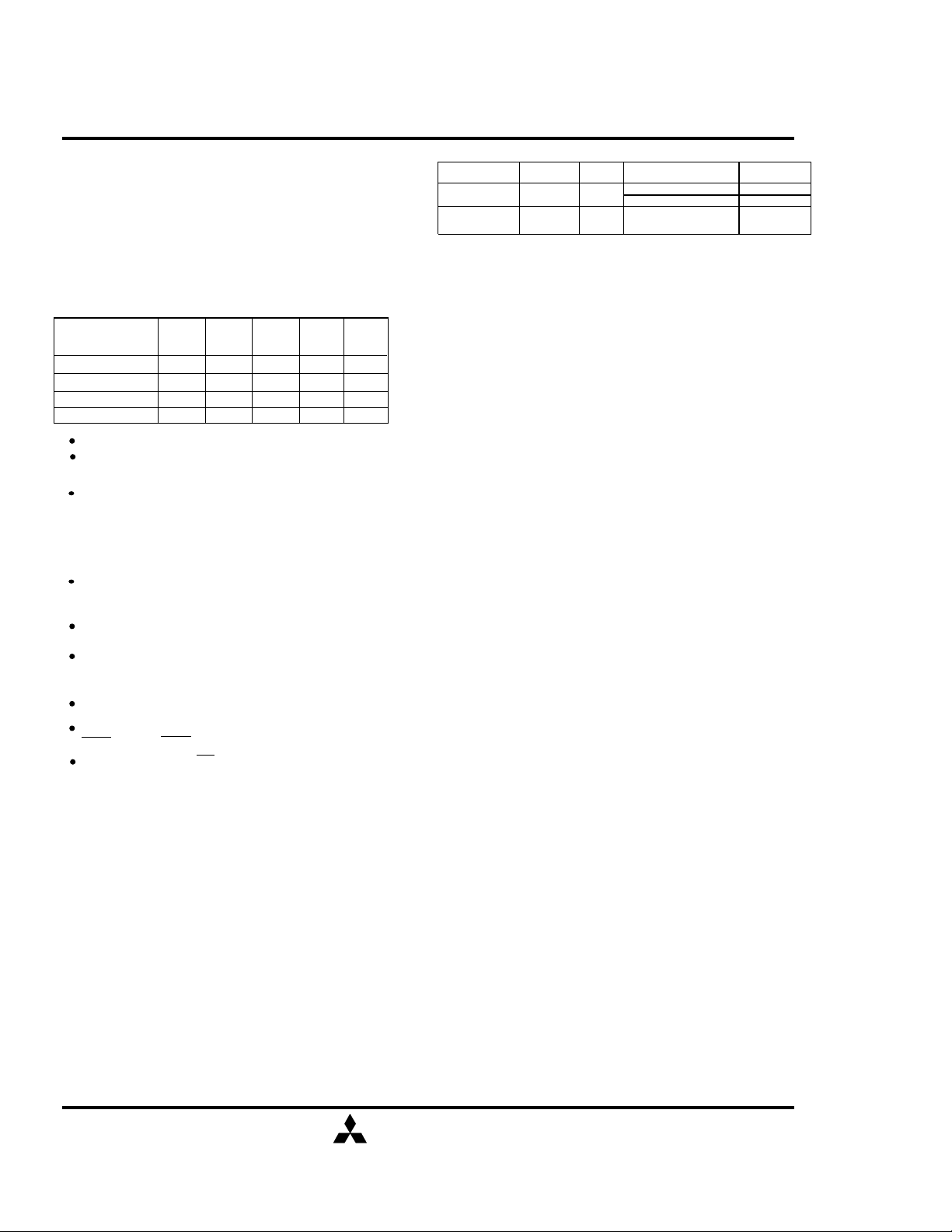
RAS
access
time
(max.ns)
MH4V64AXJJ-5,5S
MH4V64AXJJ-6,6S
MH4V644AXJJ-5,5S
single 3.3V± 0.3V supply
Low stand-by power dissipation
7.2mW- - - - - - - - - LVCMOS input level
operating power dissipation
MH4V64AXJJ-5,5S - - - - - 1584 mW(max.)
MH4V64AXJJ-6,6S - - - - - 1440mW(max.)
MH4V644AXJJ-5,5S - - - - 2016 mW(max.)
MH4V644AXJJ-6,6S - - - - 1872 mW(max.)
Self refresh capability*
Self refresh current - - - - 1600 uA(max.)
CAS
Address
access
access
time
(max.ns)
50
60
50
60 15 30 11015MH4V644AXJJ-6,6S
time
(max.ns)
13
15
13
OE
time
13
15
13
Cycle
time
(min.ns)
90
110
90
access
(max.ns)
25
30
25
ADDRESS
Part No.
MH4V64AXJJ
MH4V644AXJJ
Row Add. Col Add.
A0~A12 A0~A8
A0~A11 A0~A9
Refresh
/RAS only Ref,Normal R/W
CBR Ref,Hidden Ref
/RAS only Ref,Normal R/W
CBR Ref,Hidden Ref
Refresh
Cycle
8192/64ms
4096/64ms
4096/64ms
APPLICATION
Main memory unit for computer,Microcomputer
memory,Refresh memory for CRT.
*:Applicable to self refresh version(MH4V64/644AXJJ-5S,-6S)
only
All input, output LVTTL compatible and low capacitance
Utilizes industry standard 4Mx16 RAMs in TSOP
and industry standard EEPROM in TSSOP.
Includes decoupling capacitor(0.22uFx4)
Fast page mode , Read-modify-write,
CAS before RAS refresh,Hidden refresh capabilities.
Early-write mode,OE to control output buffer
impedance.
MIT-DS-0072-0.5 26/Feb./1997
MITSUBISHI
ELECTRIC
( / 25 )
1
Preliminary
Preliminary
Some of contents are subject
to change without notice.
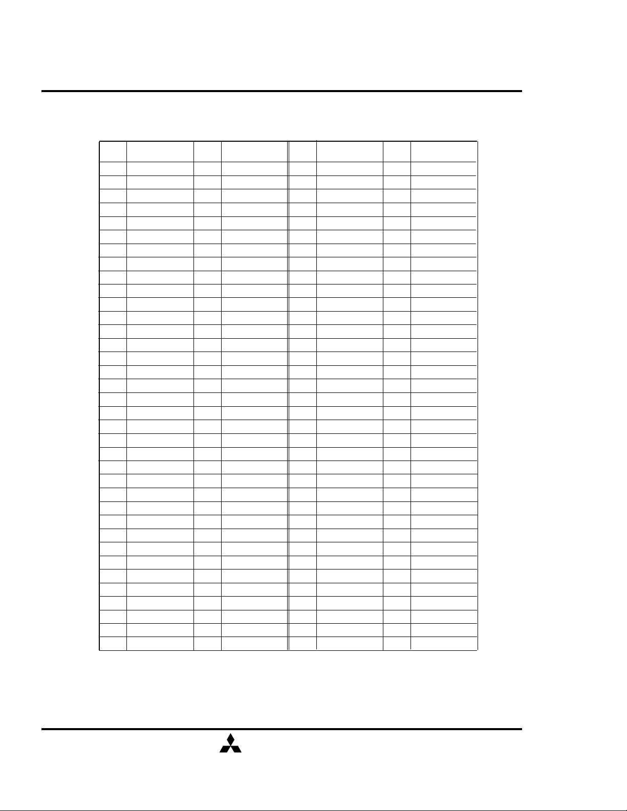
PIN CONFIGURATION
MITSUBISHI LSIs
MH4V64/644AXJJ-5,-6,-5S,-6S
FAST PAGE MODE 268435456-BIT (4194304-WORD BY 64-BIT)DYNAMIC RAM
PIN
Number
11
13
15
17
19
21 22 93 94
23 24
25 26 97 98
27 28 99 100
29 30 101 102
31 32 103 104
33 34 105 106
35 36 107 108
37 38 109 110
39 40 111 112
41 42 113 114
43 44 115 116
45 46 117 118
47 48 119 120
49 50 121 122
51 52 123 124
53 54 125 126
55 56 127 128
57 58 129 130
59 60 131 132
61 62 133 134
63 64 135 136
65 66 137 138
67 68 139 140
69 70 141 142
71 72 143 144
Front side
Pin Name
1
3
5
7
9
Vss
DQ0
DQ1
DQ2
DQ3
Vcc
DQ4
DQ5
DQ6
DQ7
Vss Vss DQ20 DQ52
/CAS0 /CAS4 DQ21 DQ53
/CAS1 /CAS5 DQ22 DQ54
Vcc Vcc DQ23 DQ55
A0 A3 Vcc Vcc
A1 A4 A6 A7
A2 A5 A8 A11
Vss Vss Vss Vss
DQ8 DQ40 A9 A12/NC(note)
DQ9 DQ41 A10 NC
DQ10 DQ42 Vcc Vcc
DQ11 DQ43 /CAS2 /CAS6
Vcc Vcc /CAS3 /CAS7
DQ12 DQ44 Vss Vss
DQ13 DQ45 DQ24 DQ56
DQ14 DQ46 DQ25 DQ57
DQ15 DQ47 DQ26 DQ58
Vss Vss DQ27 DQ59
Reserved Reserved Vcc Vcc
Reserved Reserved DQ28 DQ60
RFU FRU DQ29 DQ61
Vcc Vcc DQ30 DQ62
RFU RFU DQ31 DQ63
/WE RFU Vss Vss
/RAS0 RFU SDA SCL
NC RFU Vcc Vcc
PIN
Number
2
4
6
8
10
12
14
16
18
20
Back side
Pin Name
Vss
DQ32
DQ33
DQ34
DQ35
Vcc
DQ36
DQ37
DQ38
DQ39
PIN
Number
73 74
75 76
77
79 80
81 82
83 84
85
87
89 90
91 92
95
Front side
Pin Name
/OE RFU
Vss Vss
Reserved Reserved
Reserved Reserved
Vcc Vcc
DQ16 DQ48
DQ17 DQ49
DQ18 DQ50
DQ19 DQ51
Vss Vss
RFU:Reserved Future Use
NC,RFU,Reserved: NO CONNECTION
PIN
Number
78
86
88
96
Back side
Pin Name
Note:A12 ... MH4V64AXJJ , NC ... MH4V644AXJJ
MIT-DS-0072-0.5 26/Feb./1997
MITSUBISHI
ELECTRIC
( / 25 )
2
Preliminary
Preliminary
Some of contents are subject
to change without notice.
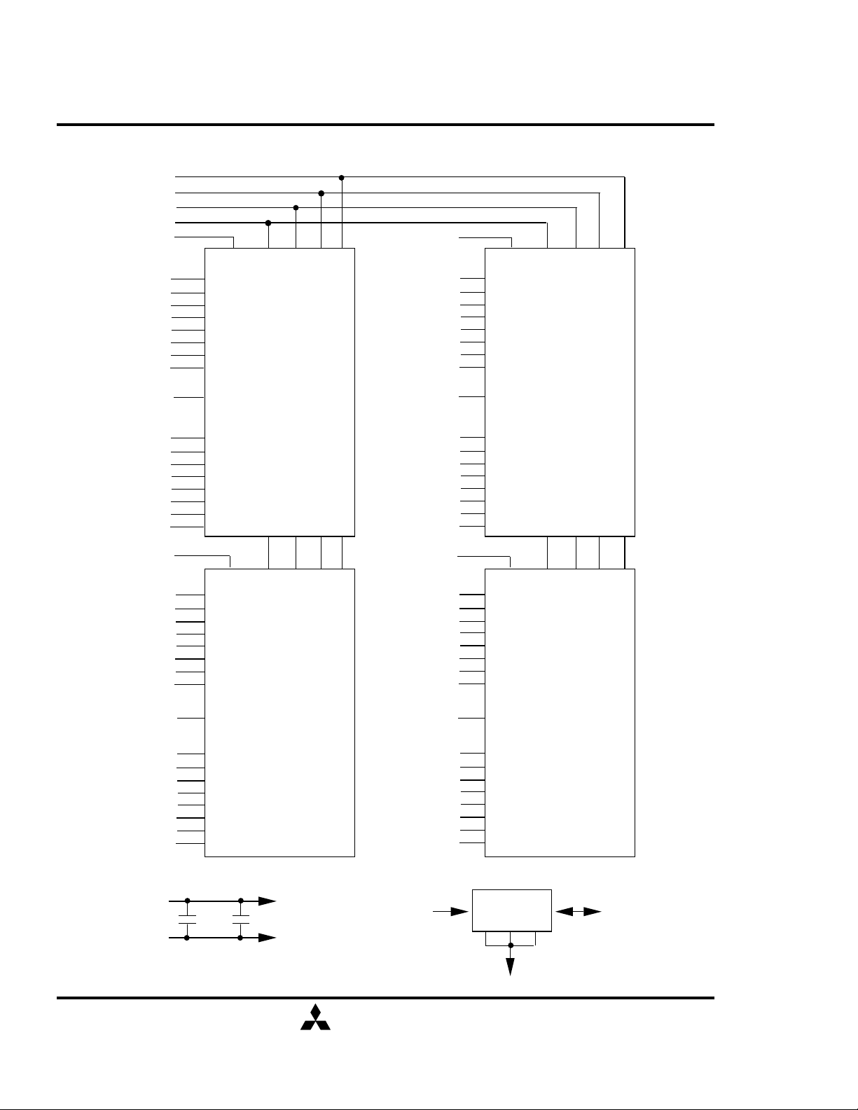
Block Diagram
Address
/OE
/WE
/RAS0
/CAS0
DQ0
DQ1
DQ2
DQ3
DQ4
DQ5
DQ6
DQ7
MH4V64/644AXJJ-5,-6,-5S,-6S
FAST PAGE MODE 268435456-BIT (4194304-WORD BY 64-BIT)DYNAMIC RAM
/LCAS /RAS /WE /OE
I/O1
I/O2
I/O3
I/O4
I/O5
I/O6
I/O7
I/O8
/CAS4
DQ32
DQ33
DQ34
DQ35
DQ36
DQ37
DQ38
DQ39
MITSUBISHI LSIs
/LCAS /RAS /WE /OE
I/O1
I/O2
I/O3
I/O4
I/O5
I/O6
I/O7
I/O8
/CAS1
DQ8
DQ9
DQ10
DQ11
DQ12
DQ13
DQ14
DQ15
/CAS2
DQ16
DQ17
DQ18
DQ19
DQ20
DQ21
DQ22
DQ23
/CAS3
DQ24
DQ25
DQ26
DQ27
DQ28
DQ29
DQ30
DQ31
/UCAS
I/O9
I/O10
I/O11
I/O12
I/O13
I/O14
I/O15
I/O16
/LCAS /RAS /WE /OE
I/O1
I/O2
I/O3
I/O4
I/O5
I/O6
I/O7
I/O8
/UCAS
I/O9
I/O10
I/O11
I/O12
I/O13
I/O14
I/O15
I/O16
D0
D1
/CAS5
DQ40
DQ41
DQ42
DQ43
DQ44
DQ45
DQ46
DQ47
/CAS6
DQ48
DQ49
DQ50
DQ51
DQ52
DQ53
DQ54
DQ55
/CAS7
DQ56
DQ57
DQ58
DQ59
DQ60
DQ61
DQ62
DQ63
/UCAS
I/O9
I/O10
I/O11
I/O12
I/O13
I/O14
I/O15
I/O16
/LCAS /RAS /WE /OE
I/O1
I/O2
I/O3
I/O4
I/O5
I/O6
I/O7
I/O8
/UCAS
I/O9
I/O10
I/O11
I/O12
I/O13
I/O14
I/O15
I/O16
D2
D3
SERIAL PD
Vcc
C1~C4
Vss
MIT-DS-0072-0.5 26/Feb./1997
D0 to D3
D0 to D3
SCL
MITSUBISHI
A0 A1 A2
Vss
SDA
ELECTRIC
( / 25 )
3
MITSUBISHI LSIs
Preliminary
Preliminary
Some of contents are subject
to change without notice.
FAST PAGE MODE 268435456-BIT (4194304-WORD BY 64-BIT)DYNAMIC RAM
MH4V64/644AXJJ-5,-6,-5S,-6S
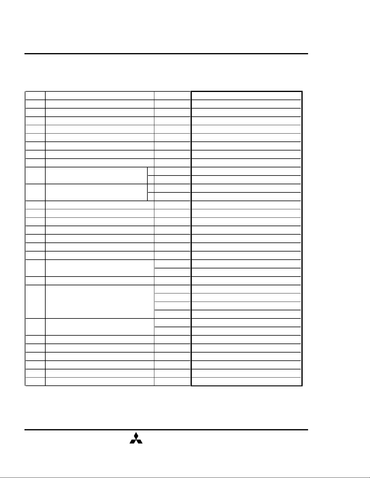
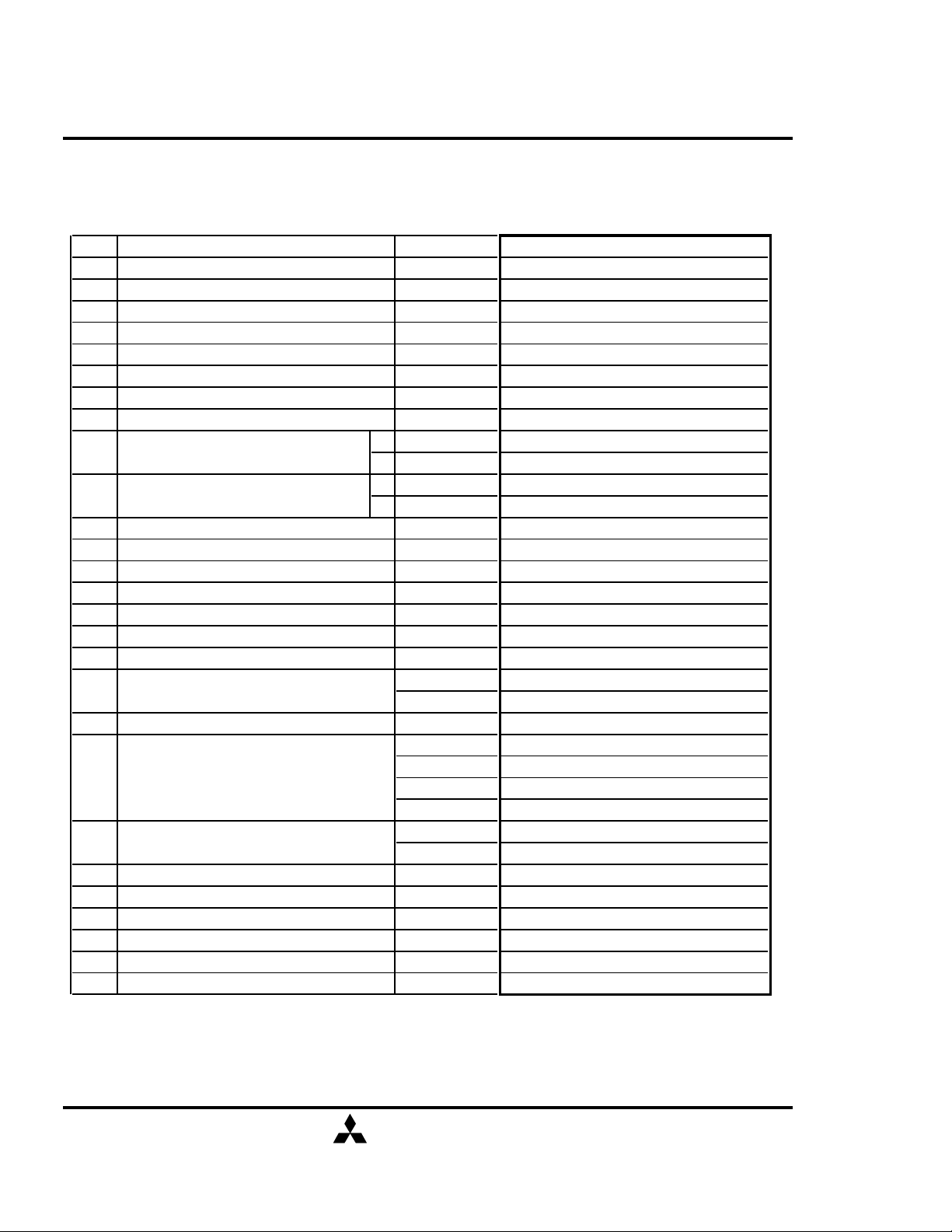
Serial Presence Detece TABLE (MH4V64AXJJ-5,-6)
Bytes Function described SPD entry data SPD DATA entry(Hex)
1 Total # bytes of SPD memory device 256 Bytes 08
2 Fundamental memory type FPM DRAM 01
3 # Row Addresses on this assembly A0-A12 0D
4 # Column Addresses on this assembly A0-A8 09
5 # Module Banks on this assembly 1bank 01
6 Data Width of this assembly... x64 40
7 ... Data Width continuation 0 00
8 Voltage interface standard of this assembly 3.3V LVTTL 02
9 RAS# access time of this assembly -5 50ns 32
-6 60ns 3C
10 CAS# access time of this assembly -5 13ns 0D
-6 15ns 0F
11 DIMM Configuration type (Non-parity,Parity,ECC) non parity 00
12 Refresh Rate/Type N/R(15.625uS) 00
13 DRAM width,Primary DRAM x16 10
14 Error Checking DRAM data width N/A 00
15-31 Reserved for future offerings open 00
32-61 Superset Memory type(may be used in future) open 00
62 SPD Data Revision Code Rev 1 01
63 Checksum for bytes 0-62 Check sum for -5 32
Check sum for -6 3E
64-71 Manufacturers JEDEC ID code per JEP-106 MITSUBISHI 1CFFFFFFFFFFFFFF
72 Manufacturing location Miyoshi,Japan 01
Tajima,Japan 02
NC,USA 03
Germany 04
73-90 Manufacturer's Part Number MH4V64AXJJ-5 4D483456363441584A4A2D352D35202020202020
MH4V64AXJJ-6 4D483456363441584A4A2D362D36202020202020
91-92 Revision Code PCB revision rrrr
93-94 Manufacturing date year/week code yy/ww
95-98 Assembly Serial Number serial number ssssssss
99-125 Manufacturer Specific Data open 00
126-127 Reserved open 00
128-255 Open User Free-Form area not defined open 00
MIT-DS-0072-0.5 26/Feb./1997
MITSUBISHI
ELECTRIC
( / 25 )
4
MITSUBISHI LSIs
Preliminary
Preliminary
Some of contents are subject
to change without notice.
FAST PAGE MODE 268435456-BIT (4194304-WORD BY 64-BIT)DYNAMIC RAM
MH4V64/644AXJJ-5,-6,-5S,-6S
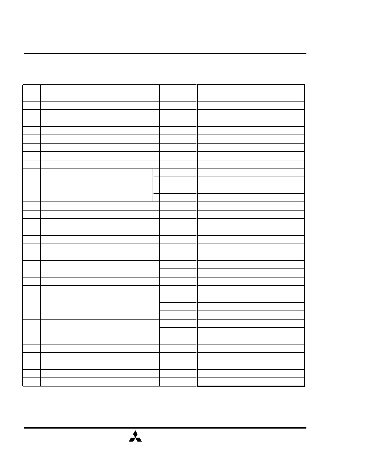
Serial Presence Detece TABLE (MH4V64AXJJ-5S,-6S)
Bytes Function described SPD entry data SPD DATA entry(Hex)
1 Total # bytes of SPD memory device 256 Bytes 08
2 Fundamental memory type FPM DRAM 01
3 # Row Addresses on this assembly A0-A12 0D
4 # Column Addresses on this assembly A0-A8 09
5 # Module Banks on this assembly 1bank 01
6 Data Width of this assembly... x64 40
7 ... Data Width continuation 0 00
8 Voltage interface standard of this assembly 3.3V LVTTL 02
9 RAS# access time of this assembly -5S 50ns 32
-6S 60ns 3C
10 CAS# access time of this assembly -5S 13ns 0D
-6S 15ns 0F
11 DIMM Configuration type (Non-parity,Parity,ECC) non parity 00
12 Refresh Rate/Type S/R(15.625uS) 80
13 DRAM width,Primary DRAM x16 10
14 Error Checking DRAM data width N/A 00
15-31 Reserved for future offerings open 00
32-61 Superset Memory type(may be used in future) open 00
62 SPD Data Revision Code Rev 1 01
63 Checksum for bytes 0-62 Check sum for -5 B2
Check sum for -6 BE
64-71 Manufacturers JEDEC ID code per JEP-106 MITSUBISHI 1CFFFFFFFFFFFFFF
72 Manufacturing location Miyoshi,Japan 01
Tajima,Japan 02
NC,USA 03
Germany 04
73-90 Manufacturer's Part Number MH4V64AXJJ-5S 4D483456363441584A4A2D355335532020202020
MH4V64AXJJ-6S 4D483456363441584A4A2D365336532020202020
91-92 Revision Code PCB revision rrrr
93-94 Manufacturing date year/week code yy/ww
95-98 Assembly Serial Number serial number ssssssss
99-125 Manufacturer Specific Data open 00
126-127 Reserved open 00
128-255 Open User Free-Form area not defined open 00
MIT-DS-0072-0.5 26/Feb./1997
MITSUBISHI
ELECTRIC
( / 25 )
5
MITSUBISHI LSIs
Preliminary
Preliminary
Some of contents are subject
to change without notice.
FAST PAGE MODE 268435456-BIT (4194304-WORD BY 64-BIT)DYNAMIC RAM
MH4V64/644AXJJ-5,-6,-5S,-6S
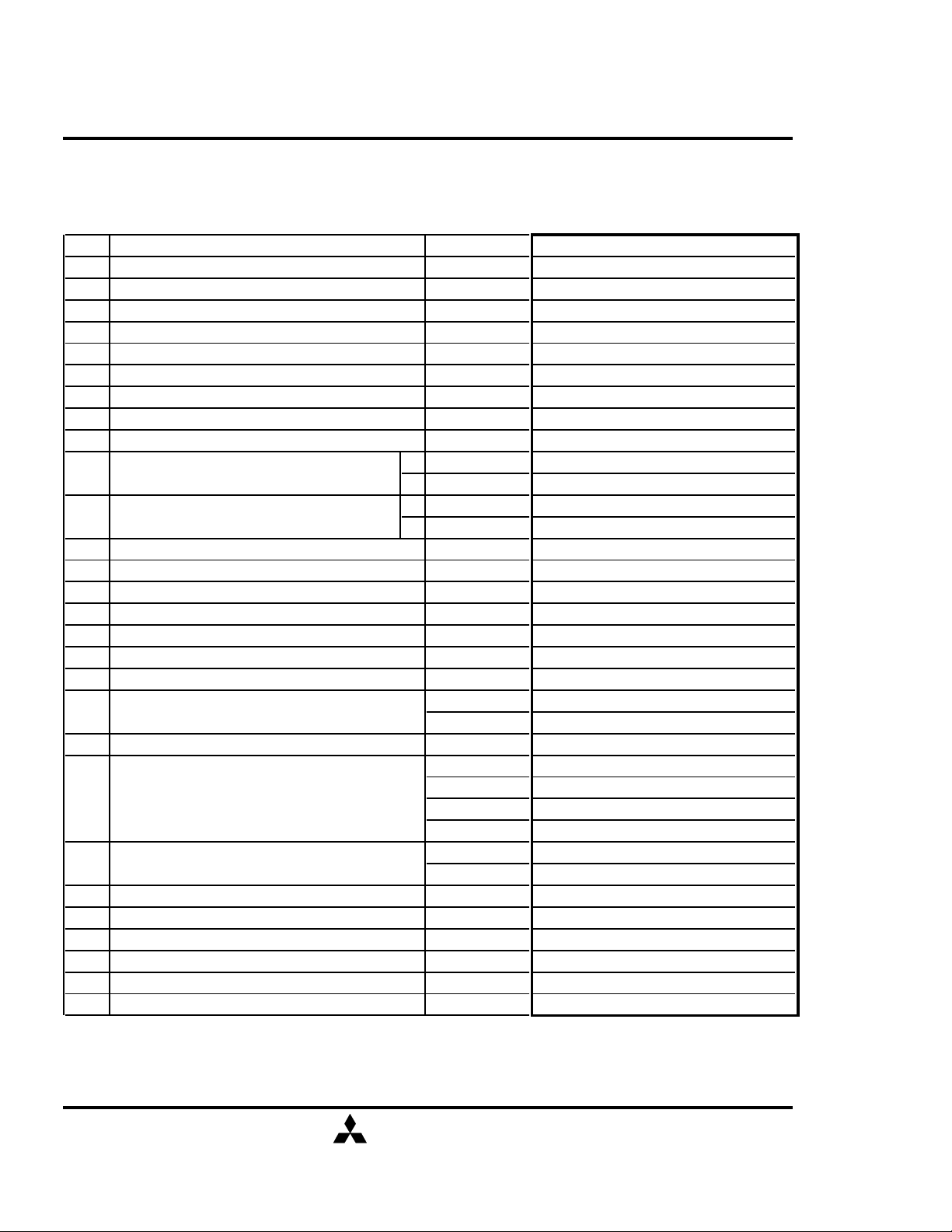
Serial Presence Detece TABLE (MH4V644AXJJ-5,-6)
Bytes Function described SPD entry data SPD DATA entry(Hex)
0 Defines # bytes written into serial memory at module mfgr 128 80
1 Total # bytes of SPD memory device 256 Bytes 08
2 Fundamental memory type FPM DRAM 01
3 # Row Addresses on this assembly A0-A11 0C
4 # Column Addresses on this assembly A0-A9 0A
5 # Module Banks on this assembly 1bank 01
6 Data Width of this assembly... x64 40
7 ... Data Width continuation 0 00
8 Voltage interface standard of this assembly 3.3V LVTTL 02
9 RAS# access time of this assembly -5 50ns 32
-6 60ns 3C
10 CAS# access time of this assembly -5 13ns 0D
-6 15ns 0F
11 DIMM Configuration type (Non-parity,Parity,ECC) non parity 00
12 Refresh Rate/Type N/R(15.625uS) 00
13 DRAM width,Primary DRAM x16 10
14 Error Checking DRAM data width N/A 00
15-31 Reserved for future offerings open 00
32-61 Superset Memory type(may be used in future) open 00
62 SPD Data Revision Code Rev 1 01
63 Checksum for bytes 0-62 Check sum for -5 32
Check sum for -6 3E
64-71 Manufacturers JEDEC ID code per JEP-106 MITSUBISHI 1CFFFFFFFFFFFFFF
72 Manufacturing location Miyoshi,Japan 01
Tajima,Japan 02
NC,USA 03
Germany 04
73-90 Manufacturer's Part Number MH4V644AXJJ-5 4D48345636343441584A4A2D352D352020202020
MH4V644AXJJ-6 4D48345636343441584A4A2D362D362020202020
91-92 Revision Code PCB revision rrrr
93-94 Manufacturing date year/week code yy/ww
95-98 Assembly Serial Number serial number ssssssss
99-125 Manufacturer Specific Data open 00
126-127 Reserved open 00
128-255 Open User Free-Form area not defined open 00
MIT-DS-0072-0.5 26/Feb./1997
MITSUBISHI
ELECTRIC
6
( / 25 )
MITSUBISHI LSIs
Preliminary
Preliminary
Some of contents are subject
to change without notice.
FAST PAGE MODE 268435456-BIT (4194304-WORD BY 64-BIT)DYNAMIC RAM
MH4V64/644AXJJ-5,-6,-5S,-6S
Serial Presence Detece TABLE (MH4V644AXJJ-5S,-6S)
Bytes Function described SPD entry data SPD DATA entry(Hex)
0 Defines # bytes written into serial memory at module mfgr 128 80
1 Total # bytes of SPD memory device 256 Bytes 08
2 Fundamental memory type FPM DRAM 01
3 # Row Addresses on this assembly A0-A11 0C
4 # Column Addresses on this assembly A0-A9 0A
5 # Module Banks on this assembly 1bank 01
6 Data Width of this assembly... x64 40
7 ... Data Width continuation 0 00
8 Voltage interface standard of this assembly 3.3V LVTTL 02
9 RAS# access time of this assembly -5S 50ns 32
-6S 60ns 3C
10 CAS# access time of this assembly -5S 13ns 0D
-6S 15ns 0F
11 DIMM Configuration type (Non-parity,Parity,ECC) non parity 00
12 Refresh Rate/Type S/R(15.625uS) 80
13 DRAM width,Primary DRAM x16 10
14 Error Checking DRAM data width N/A 00
15-31 Reserved for future offerings open 00
32-61 Superset Memory type(may be used in future) open 00
62 SPD Data Revision Code Rev 1 01
63 Checksum for bytes 0-62 Check sum for -5S B2
Check sum for -6S BE
64-71 Manufacturers JEDEC ID code per JEP-106 MITSUBISHI 1CFFFFFFFFFFFFFF
72 Manufacturing location Miyoshi,Japan 01
Tajima,Japan 02
NC,USA 03
Germany 04
73-90 Manufacturer's Part Number MH4V644AXJJ-5S 4D48345636343441584A4A2D3553355320202020
MH4V644AXJJ-6S 4D48345636343441584A4A2D3653365320202020
91-92 Revision Code PCB revision rrrr
93-94 Manufacturing date year/week code yy/ww
95-98 Assembly Serial Number serial number ssssssss
99-125 Manufacturer Specific Data open 00
126-127 Reserved open 00
128-255 Open User Free-Form area not defined open 00
MIT-DS-0072-0.5 26/Feb./1997
MITSUBISHI
ELECTRIC
( / 25 )
7
MITSUBISHI LSIs
Preliminary
Preliminary
Some of contents are subject
to change without notice.
FAST PAGE MODE 268435456-BIT (4194304-WORD BY 64-BIT)DYNAMIC RAM
MH4V64/644AXJJ-5,-6,-5S,-6S
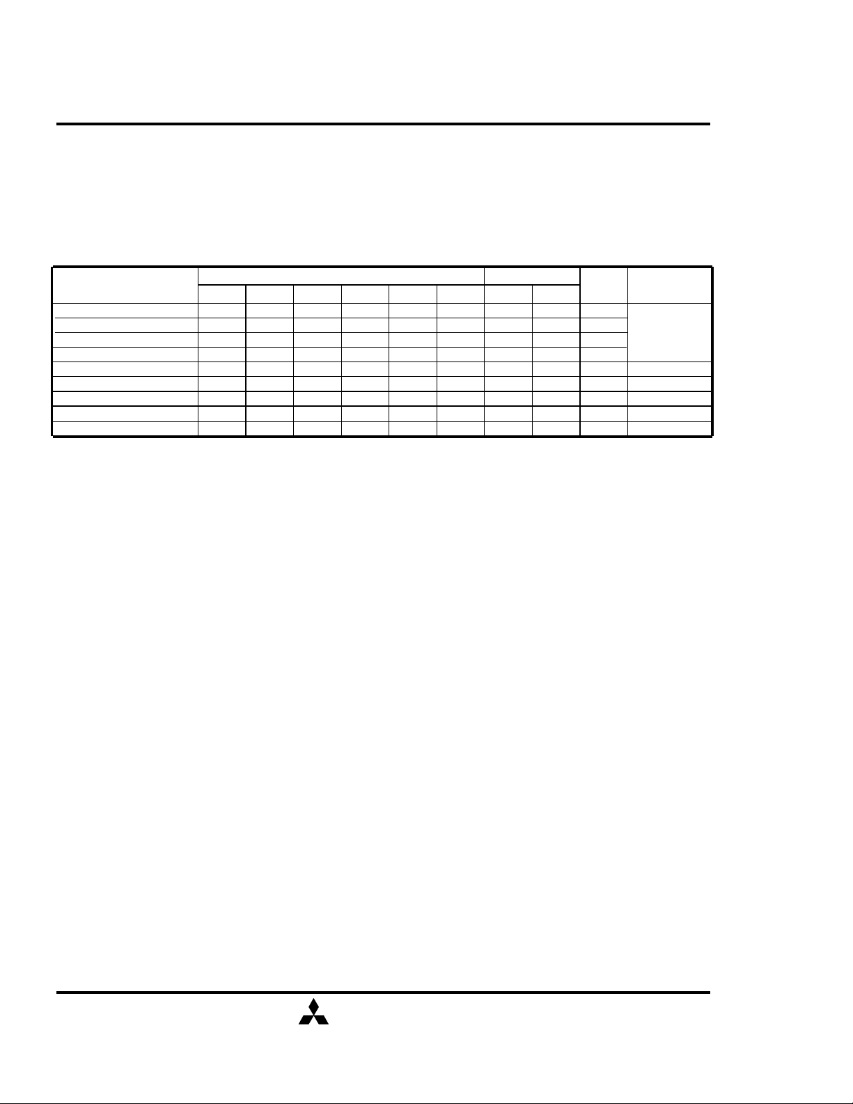
FUNCTION
The MH4V64/644AXJJ provide, in addition to
normal read, write, and read-modify-write
operations,
Table 1 Input conditions for each mode
Operation
Read
Write (Early write)
Write (Delayed write)
Read-modify-write
/RAS-only refresh
Hidden refresh
/CAS before /RAS refresh
Standby
Self refresh
Note : ACT : active, NAC : nonactive, DNC : don' t care, VLD : valid, IVD : Invalid, APD : applied, OPN : open
*MH4V64/644AXJJ-5S,-6S only
*
/RAS /CAS
ACT
ACT
ACT
ACT
ACT
ACT
ACT
NAC
ACT ACT NAC DNC OPN YESDNC DNC DNC
ACT
ACT
ACT
ACT
NAC
ACT
ACT
DNC
Inputs Input/Output
/W
NAC
ACT
ACT
ACT
DNC
NAC
NAC
DNC
a number of other functions, e.g., Fast page mode,
/RAS-only refresh, and delayed-write. The input
conditions for each are shown in Table 1.
/OE
address address
ACT
DNC
DNC
ACT
DNC
ACT
DNC
DNC
Row
APD
APD
APD
APD
APD
APD
DNC
DNC
Column
APD
APD
APD
APD
DNC
DNC
DNC
DNC
Input
OPN
VLD
VLD
VLD
DNC
OPN
DNC
DNC
Output
Refresh Remark
VLD
OPN
IVD
VLD
OPN
VLD
OPN
OPN
YES
YES
YES
YES
YES
YES
YES
NO
Fast page
mode
identical
MIT-DS-0072-0.5 26/Feb./1997
MITSUBISHI
ELECTRIC
( / 25 )
8
 Loading...