

Page 1

UGD-0344A
5.25
INCH FLEXIBLE DISK
TECHNICAL MANUAL
MF504A-3
DRIVE
AMITSUBISHI
ELECTRIC
CORPORATION
Page 2

CHAPTER 1
1.1
1.2
CHAPTER 2
2.1
2.2
2.3
2.4
CHAPTER 3
3.1
3.2
3.3
3.4
3.5
3.6
3.7
3.8
3.9
3.10
3.11
3.12
CONTENTS
LINE
OUT
Composition of Mechanism by Function
Composition of Electronic Circuitry
MECHANISM
DESCRIPTION
Rotation
Disk
Magnetic H,ad-Positioning
Magnetic Head/Carriage Mechanism . . . . . . . . . . . . . . . . . . .
(Index,
Sensors
DESCRIPTION
Inter.ace and Drive Select Circuits
Power-On Reset and Power
Panel Indicator Circuit .
Sensor
Index
Motor
Step
00
Track
Select
Side
Write/Erase Circuits
Write-Protect Circuit
Circuit
Read
Write Current Switch Circuit . . .
Motor
Spindle
Drive
Write
and
Drive Circuit
Detection
Circuit
............
Drive Circuit
OF
Clamp Mechanism
and
Drive
Protect,
ELECTRONIC
OF
Save
_
...
Ready Circuits
........................
.........................
Circuit
.
.....
..
.
....
.................................
Track
...
Function
by
OPERATION
..............
Mechanism
........................
................................
00)
CIRCUIT
....
Circuits.
............................
..................................
.
OPERATION
.
.
...........
.
2
2
2
3
4
11
12
13
13
14
1.4
15
5
6
9
9
.
.
.
.
.
16
19
19
22
.
23
-1-
Page 3

1.
This section deals
flexible
compatible
However,
signal
switched
In
addition,
only
1.1
Composition
The mechani-sm
(1}
(2) Disk
{3)
{4)
(5) Sensors
1.2
Composition
The
The
motor.
( 1)
(21
(3~
(4)
(5)
(6)
(7)
(8}
(9)
(10)
(11)
disk
unit
with
normal
for
360/JOOrpm
at
the
it
is
the
READ/WRITE
of
Lever
mechanism
rotation
Magnetic
Magnetic
{index,
of
electronic
spindle
motor
Signal
interface
Power-on
Panel
indicator
Index
pulse
Step
motor
Track
00
Side select
Write/erase
Write-protect
Read
circuit
Spindle
motor
CHAPTER 1 OUT LINE
with
the
mechanical parts
with
high
density
48TPI
medium
high
and
to
set
the
is
switched.
by
Function
by
funciton as follows:
door
sw
mechanism
mechanism
mechanism
protect,
Circuitry
installed
constitutes
and
drive select
circuit
circuit
circuit
medium
normal
unit
mechanism
track
by
Function
an
two
and
ready
a 8 inch flexible disk allowing
density
for
same
time.
also posible
circuit
mechanitm
can
be
divided
and
and
clamp
head
positioning
head/carriage
write
Electronic
circuits
are
drive
circuit
circuit
reset
circuit
drive
generator
drive
circuit
detection
circuit
circuit
circuit
circuit
drive
and
control
for
the
reading
be
read.
respectively.
circuits
more
can
density
allows
only
for normal density so
00)
printed-circuit
an
independent
circuit
circuit
of
the
than
lMB
and
writing
The
rotational
The
READ/WRITE
that
the
boards
and
printed-circuit
MF504A-3
flexible
formatted
memory
of
previously used normal
speed
can
be
switched
circuitry
disk
rotational speed remains
can
be
classified
which
is
by
built
board
drive.
capacity.
is
also
at
function
integrally
M
F504A-3
It
is
format
density
disks.
by
an
external
automatically
360rpm
as follows:
with
and
the
Page 4
Screw
Sub Base
bridge
l
Qt
\
Indicator (LED)
Screw
\
Diecast
frame
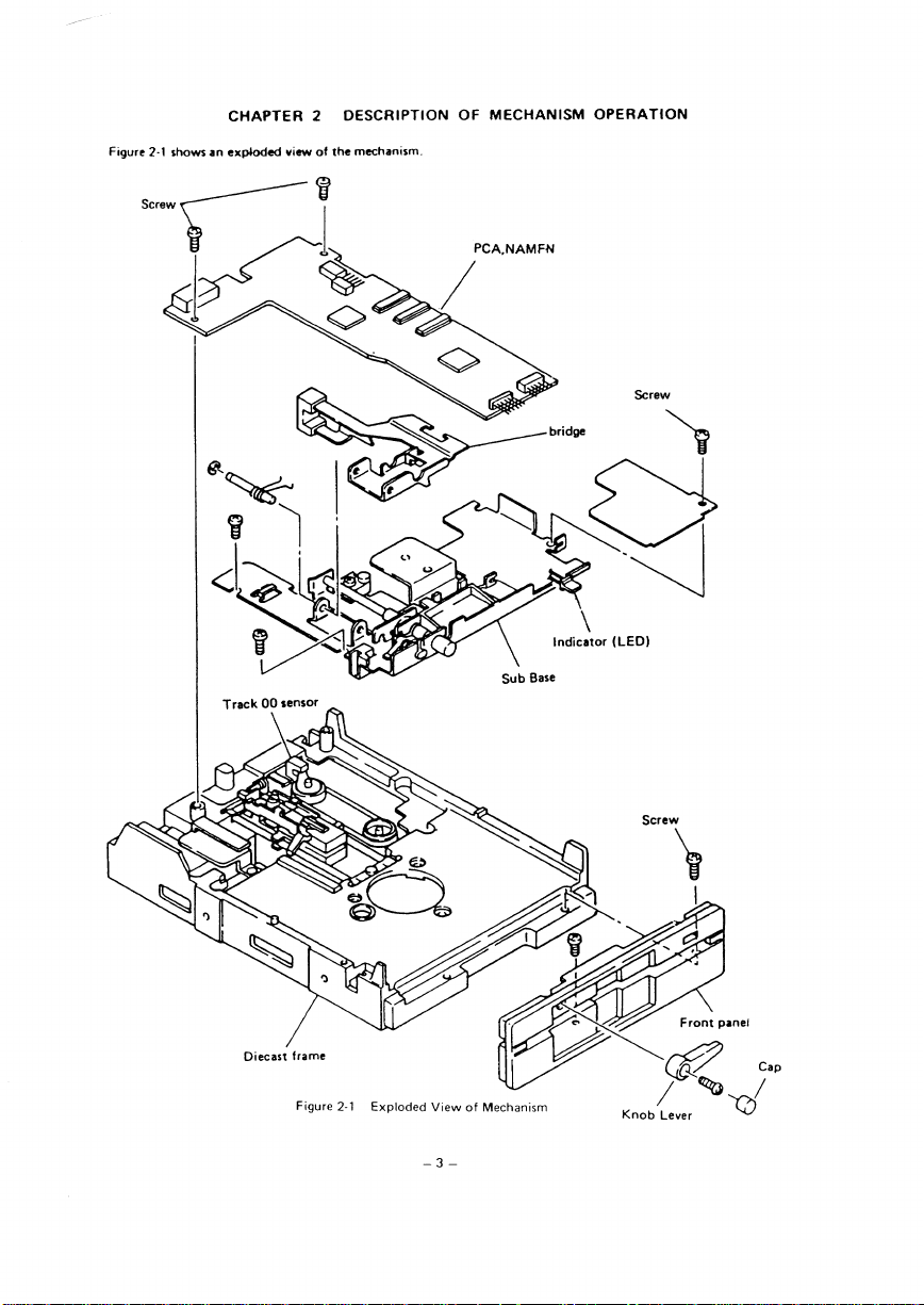
Figure
2-1
Exploded
-3-
v·
iew
Mechanism
of
/~
L
Knob
ever
y-/
V
Cap
Page 5

2.1
Oiik
Rotatton
The disk
rotation
because
it
ts
The
motor
does
spindle directly connected
rotation mechanism
300rpm
and this can be swiched by
The
frequency-genentor
The disk
is
to
clamped
•
position
disk
the disk drives.
The
collet
is
Figure 2-2 shows
The printed-circuit
disk
rotation
signal. And a
Collet assmbly
Spindle
Index sensor
(LEO)
Driff
•nd
Cl•mp
MKh•nism
drive
motor
a b<ushtess
not use
is
type
that
ulft
1
belt, unlike C10nventional C10unt1<pwts,
to
uch
is
completely free
coil detects the spindle
by
the
spindle cone
on
the
inner surfoce
tapered
to
• specific
the
spindle
board
detection,
photo
transistor for receiving its light
•ngl•
motor
tor
the
write protect
cone
1
flit
DC
servo
1
othef. This
the
motor.
H1H
element for coil phase-switching
is
onother feature for p<olonging motor life
of
maintenance.
PCA.
NAMFM signals
motor
on
the
motor
of
the
spindle
to
correct non..,lignment
end
collet.
spindle
motor
-vo
sensor LED
for
is
This motor has as
The
rotational speed
trom
speed
1nd
torms
side
and
by
cone.
This assures compotibility
ot
circuit
hH
an
write
protect
installed
on
another printed-circuit
Jong
1
life
11
1n
ordinary
Mtectton.
but
it
1
direct«iw
of
the
the
main control circuit.
•-YO
the
C10llet
circuit
on
the
spindle
an inserted disk with
type
to
C10ntrol
door.
the
~
tpindle
with
Ind
motor
The
the
ouuring
is
360rpm
it.
CIOllet
diskettes
cone.
AC
rotor
thet
guides
index sensor LED (lifht-emitting diode) for
defection and indicator LED
board
for
(NAMFM).
driving
motor
1nd
the
and
the
end
Figure 2·2 Spindle
-4-
Motor
and Collet
Page 6

Maitnttttc HMd-f'ositioninig
2.2
step
flat
The
step
oppostte
is
distance.
Figure
motor
fastened
2-3
shaft
the
to
shows
motor
steel
the
drives
hm
band
steel
positioning
the
Ori-.ie
magnetic
the
thin~oop
1
m.intain
to
that
so
band
Medt•niMn
head
~nd,
steel
specific
a
turn
a
mechanism.
drive
to
which
of
each
tension.
step
the
track
is
pulled
The
motor
(cylinder)
spring attached
the
by
head/carriage
one
by
succession.
m
assembly,
angle
step
The
1upported
moves
to
the
upstan
idler pulley
the
head
mounted
by
by
two
single
1
guide
the
on
located
rods,
track
Figure 2-3 Magnetic-Head
Step
Positioning
assy
motor
Mechanism
Head/carriage
assembly
-5-
Page 7

(Index.
Sant0n
2.4
sensor
Index
( 1)
index
The
transistor
photo
motor(Figuro
Index sensor timing (position) can
index sensor.
Figure 2-6 shows where
(2) Writ&-p<Otect sensor
writ&-protect senso<
The
This sensor
with
Disks
sensor.
protect
sub-base,
the
00
Track
(31
track
The
track
The
assembly.
screw.
track
The
Protect.
Writ•
sensor
2-2).
protects
diskette's
the
Remember
disk~
the
this
sensor
sensor
00
sensor
00
sensor
The
sensor
00
Trod< 00)
rotation.
disk
detects
light·recei..,ing side.
the
on
photo
the
ind
photo-transistor for
the
the
detects
information
that
The
stored
covered
notch
or
vinyl
write-protect sensor
will transmit signals
that
detects
the
detects
screwed
is
head/carriage assembly are
and
This sensor consists of
The
mounted
is
tronsistor
adjusted
be
write-protect notch
diskette's
read-only disks from
on
tape
with
to
head
position
the
to
is
PCA.]
is
of
STM.
tape
mounted
on
the
cellophane
the
mounted
ts
LED
the main control
on
the
loosening
by
index: sensor
the
that
,..,
1
or
a high percentage
has
that
sub-base ash shown
on
00
track
light-shielding plate
holder
shown
and
in Figure
can
LED
an
the
on
screws
mounted.
is
inhibits
and
destruction
not
does
that
adjusted in
be
2-7.
hght-emitting
the
on
circuit PCA for
serYO
PCA (NAMFM).
circuit
index
the
on
write
operM:ion
by
litht
transmit
light transmission wilt
of
Figure 2-6.
in
projects
position
seonSOf'
operation.
errors.
protected
1re
the
from
by
and
side
spindle
the
removing
and
by
[Attached
head/carriage
loosening
this
not
to
the
a
Write-protect
Figure 2-6 Index
sensor Disket survey lever
Sensor
Write-protect
and
sensor
-7-
Page 8

Head/carriage assembly
Figure 2-7 Track
Track
Sensor and Head/Carriage Assembly
00
00
sensor
-8-
Page 9

3·
ftgure
spindte
TM
integraUy
p.ts
The
CHAPTER
shows
1
motor
with
within
the
the
motor_
the
electrontc
circuit
drive
lines
chain
DESCRIPTION
3
circuits
within
belong
and signal
the
the
to
OF
connections
lines
dotted
mechanism
ELECTRONIC
these circuits.
among
constitutes
the
in
described
CIRCUIT
sepaute
the
previous pages.
OPERATION
printed-circuit
board
that
built
is
-9-
Page 10

-READ
-WAITE
DATA
DATA
-------------
I
RIW
IC
M5101
BAP
Read
circuit
Write
ci.-cuit
Er•e
circuit
or
MC2870P
--,
-SIDE·!
-WRITE
-WRITE
-DIRECTION
-NORMAL
-TRACK
-MOTOR
-ORIVE
-ORIVE
-ORIVE
-DRIVE
SELECT
PROTECT
GATE
-INDEX
-READY
IN
SEL
-STEP
DENSITY
00
ON
-IN
USE
SELO
SEL
SEL2
SEL3
Side
select
ci.-cult
Power
on
ruet
circuit
Wri~e
protect
detection
circuit
Write99te
circuit
Erase
gate
circuit
Index
/ready
circuit
Step
motor
drive
ci.-cuit
Track
counter
Track
00
detection
circuit
Head
load
solenoid
drive
circuit
1---1'---4
P•nel
indicator
drive
circuit
Power
1
circuit
511ve
-----------
r,--s:n:.~~;-
~
I
I
I
I
-~
.
I I
~1
~-~,~~c~t--~
Figure
3-1
MF504A-3
-10-
Electronic
Circuit
Page 11

3-1
lnterf•ce
•nd
11 ~ Receive circuit
AU
the
ohms.
capacity
In
connecting
cabte
(2) Transmit circuit
The
disk
controller
All
input
connected
controller.
(3) Drive select circuit
The
drive select circuit selects
through
The
four
inserted
drives
drives
The
drive select signals also light
In
the
MX
to
Ori••
Select
Circuits
input
terminals
of
the
pulling
them
of
40
mA
or
two
end
four
or
terminating
drive
line driver
to
use a terminating
signals
to
in
the
doisy-chain
interface lines
select lines correspond
to
select
that
will cause errors.
case
maintain
the
are
connected
of
a system requiring no drive selection. insert
a selected condition.
lece1ver
up
to
+5
V.
diik
The
drives
more. Normally.
more
resister and remove
is
an
SN7438N
rnistor
the
line driver are
pattern,
one
of
(OSO
through OS3).
to
the
desired line. Never insert plugs
with
the
same cable; interference between
the
panel indicator LEO.
that
receives
sigNls
from
the
host
con1lloller are
host controlter. therefore. must use driver elements
1n
SN7438N
or
an
equiv•lent
(up
to
fourt
by
the
terminating resistors
or
of
150
ohm1
pted
by
the
signals
the
disk drives Cfour maximum) connected with
jumper
• daisy-chain
equiv1lent open-collector gate. It
or
more.
drive select signals. Thus, if
of
only
one
plugs
on
the
into
open-collector
pattern.
of
the
other
selected disk drive are .transmitted
printedcircuit bOards,
the
same-numbered jacks
the
the
jumper plug for
drive
it
is
necessary
disk drives_
is
necessary for
two
or
more
one
on
output
signals from such disk
the
drive select line
terminated
with
is
recommended.
to
disk drives are
to
the
same cables
of
which should
two
or
a drive
keep
the
the
more
into
at
150
the
host
host
be
disk
the
-11-
Page 12

3.2
Power-On
(
1)
Power·on reset
The
1or preventing
(2) Power save circuit
The power s1ve circuit
operating
temperature
The
of
30 ms.
Timing
- STEP (TP15)
Anet
•nd
Power
S•we
Circuits
circutt
power-on reset circuit. 1 levet-detection
operation
errors of
the
write
controb
current flowing
to
reduce heat
disk drive.
head load solenoid shore
sove circuit
generllion
is
shown in figure 3-2.
step
condition
motor
chan
rise
of
of
and
the
the
po-
type
reset
drcun.
mitiailizes
the
circuit in switching power
to
the
step
motor
by
unnecessary power consumption
the
same timer (rnono-stablemultivibr1torl, which
and
control
on.
off.
head
load solenoid KCOrding
LSI.
ind
and
thus
that"s used
to
their
to
reduce
has
1 range
\
TRl-collector
output
:~2vv_-:::::::~~~~~~~~~
Figure
3·2
Power Save Circuit Timing Chart
......
~~-:~~~-'f"""""""~.._~~~~~~~~-
l
Jo
ms
,
..
-12
-
Page 13

3.3
Panel I ndK::1tor
The
panel
indicator
When
no
in-use signal
If
the
jumper
signal
only.
Regarding
Specifications MF504A-3_
3.4
signals.
The
than
When
the
Figure
Index
Sonsor
The index
ready
300
the
ready
J_J
jumper
s.en10r
circuit
ms and
door
signal is
shows
Circuit
plug for
ind
ReMly
circuit
checks
the
opens
reset.
a
timing
is
plug
next
turned
is
the
ind
on
by a drive select signal
applied
to
drive select
combination
Circuits
detects
the
the
index pulse interva1s
index pulse
the
disk
chart_
the
interface,
circuit
is
and indicator
index
holes
is
generated_
stops
rOtating
the
inserted
conditions,
in
with
and
or
panel
the
the
by
into
disk
a
timer,
motor-on
a
dnve
indicator
the
MX,
refer
with
and
select signal
is
turned
the
panel
to
the
detailed
a
sensor,
becomes
signal
turns
and
in-use signal.
on
by
a
drive
indicator
is
description
and converts
ready
when
off
and
turned
its signals
the
the
select signal
on
by
in
the
intervals
disk
stops
only.
an
in-use
Standard
into
logic
are
rotating
less
DOOR
MOTOR
XINDEX
Timer UCG inside)
READY
CLOSE
OPEN
X. INDEX (ICGl-461
Timer
(ICGl
inside)-------'
READY
(ICG1-34J
ON
(Pl-16)
(ICGl-46)
(ICl
·341
Figure
I
.
3-3 Index
JOO
ms
I
. .
.
DOOR
open/closf·
MOTOR
Sensor
on/oft
and
Ready
Circuit Timing
"'-~~~~~~~~
Li
Chart
-13
-
Page 14

3.5
Step
Motor
Drive
The
step
motor
using
two
These
The
steP
tion
durtng
In
a seek
for
30
Figure 3-4 shows • timing
The
step
seeking
to
prevent
3.6
Track
The
track
assembly, using a sensor. This
signal.
put
is
For a timing
XDSEL flCG1·17J
is
source/sink
four
modes
motor
dritite
times
operation,
ms
or
more, +5 V
mote< drive circuit blocks
during
write
further
00
Detection Circuit
00
detection
The
circuit
on.
chart, refer
Cireutt
a two-phase bipolar
type
drivers.
are
generated
by
circuit
other
outward
will
switches
than
seeking. when
+12 V
is
supplied
is
supplied.
chart.
o-ation.
seek.
circuit detects
not
output
to
figures 3-4.
When
output
type
an
up-down
the
to
the
step
the
the
is
a signal.
the
ANDed with
and
ts
driven
four-court
voltage supplied
the
motor
is
drive
circuit.
pulses
with a write
track
00
sensor
position
of
the
the
therefore,
unless
to a "Step
angle
counter
that
the
motor
if
the
next
gate (except for
turns
the
drive phase is
uses
drive circuit
step pulse
on,
to
still.
but
output
light-shielding plate
step motor drive phase
of
1.8° by feeding four
two
flip-flops.
to
reduce
is
not
the
erase delay time)
the
circuit 1lso blocks
that
projects from
(TKOO)
at
track
00
mode
power
applied
to
the
the
to
generate a track
even if
the
currents,
consump-
the
interface
to
prevent
step
pul-
head/carriage
00
sensor
out-
-DIRECTION
SELECT (TPl-18)
-STEP
(TP151
TKOOIN (TP1)
-WAITE
GATE
(TP6)
STMP1 f!CGl-371
STMP4
llCG1·541
TK
00
iTPl:ll
IN
TO
(INHIBITI
Figure 3-4 Step
TK
I
\J
01
02
I
I
00
I
}TKOO
I
I
I
I
I
I
I
i
I
I
\
' I
\~~
Motor
Drive
Circuit
-14-
02
01
:::i
SENSE\
I
1/
I
When
TKOO
stap
pulses are inhibited
Timing Chart
03
is
enabled,
r-
Step
phase
Same interface
output
outer
moto1
changE>
Page 15

3.7
Side Select Circuit
Side
selection
is
(H1Bl.
system
ONE
SELECT
made
alternately
is
fed
se•ects
if
This
operation
and
an erase current
bias curTents
and
HOB
The
host
same interface line
Figure 3-5 shows a block diagram
SIDE
by
from
from
it is high.
Figure
switchin9
the head center tap
feeds a write
center tap
CT-0 (CT-11
side
1
~
I
current
CT·O {CT-1) to ER-0 (ER-1)
to
HO'A
(HlAI
through
the
interface
of
the
side
select
!'-----
M51018P
I
I
I
I
I
L_
-
3-5
Side Select Circuit Block Diagram
from
circuit.
or
MC2870P
-
from about 0
center
and
HOB
line
if -
Head
select
driver
--
Vat
off
tap
(HlBI
SIDE ONE
to
CT·O
(CT-11
during write operation.
to
induce a voltage
SELECT
about
to
HOA
ERO
is
0
ER1
11
(HlAI
low,
V
at
between
or
on.
In
side
Side 0
Side 1
and
HOB
(HlBI.
read operation
HOA
(H1B)
0
through
a
the
-15-
Page 16

Write/Erase
3.8
write circuit is used for recordi™] dat.a
The
~lected
true
The
data
old
l)fevents
thus
write
The
• Write
• Write driver
• R/W
• Write
1
When
operation.
-ite
changes
This differential signal
write driver
The
current
write
R/W
The
write gate.
a
3-6 shows
Figure
Current
figure, according
the
in
operation
Erase
circumferential
point
a
Therefore,
turning
the
to
for
is
It
360rpm
at
kept
be
erase
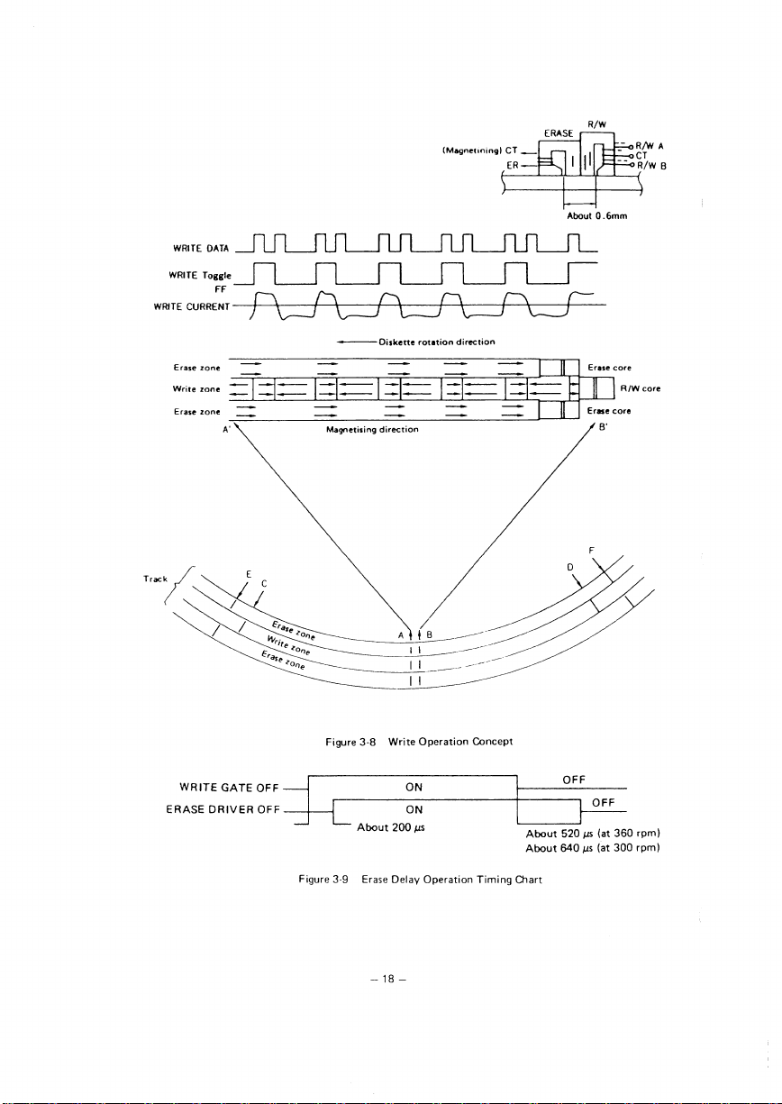
The
3-8
Figure
Circuiu
diskette
If
head.
enses
circuit
remaining
from
data
old
consists
circuit
flip-flop
to91Jle
matrix
source
current
write gate
is
Write
synchronously
is
source
feeds a
matrix
the
alternately
is
starts
position
R!W
the
that
delay
the
of
on
purpose
this
(approx.
selected.
function
shows
erases
a
~ite·protect
previous
the
either
on
in
crosstalk
following blocks:
the
of
wrtte
the
input,
counted
is
data
write
the
with
the
switch
a switching
and
erase
fed
to
with
sent
is
current
function
to
the
point
to
to
the
differential
deviation
has passed approx.
gap
core
shown in figure
operation
erase driver
the
erase delay
the
that
300rpm)
at
1000µs
from
data
conceptual
diagram
stltus
dlt•
of
side
reading
toggle flip-flop •
down
data
write driver.
that
ci«"cuit
write driver.
the
head selected
the
figure
and
head
R/W
E befor
R/W
the
of
and
after
disk
the
of
disk.
the
on
detected.
is
both
on
written
written
newty
data.
new
the
....wite
half
one
to
generated.
is
current
feeds a
by
write
3-7. a
two
through
invert its magnetization.
to
signal
write
from
timer
write
core
the
by
start
from
350µs
·9
3
closing
the
provided
is
closing
always
operation
point
is
magnetizing
s.tarts. writing when
It
open1tion
write
no
the
of
sides
due
data
driver and
write
the
by
the
to
ONE SELECT as
SIDE
block
circuit
routes, CT
current
C and ends
core
erase
the
360rpm
at
for
required
write gate
the
of
control
to
write
the
of
figure 3·9,
and
the
performed.
is
DC tfa$Ure.
by
data
devi•tion
slight
1
to
current
write
toggle flip-flop,
head. This
R/W
the
diagram.
R/WA
-+
point
at
0.6
about
is
(approx. 500µs
it
from
time
the
the
to
erase.~triver.
the
head
the
gate.
direction.
one
in
erase
an
V«ite 91te
source
and
current
write
and
after
F
mm,
300rpml
at
the
turning
must
delay
This
had
of
ere
differential
a
is
circuit
CT-+
write
the
and
opening
off
Thus,
remain
operation
opened
is
function
pasition.
enlbled
generated
gate
R/WB
point
end
erase
(near
later
the
of
the
of
approx.
for
the
on
timing
the
for
prevents
and
start
to
that
signal
the
by
opened
is
shown
as
The
0.
reaches
core
321.
TK
gate
write
erase driver.
590µs
and
track
chart.
a
by
-16-
Page 17

NC::;::
...
(Wither
Modified
WRITE
(from J20104)
NORMAL
OENSITY
Modified
ERASE
(from J20104)
NORMAL
DENSITY
SIDE
ONE
SELECT
1
remems
~
hod)
3-6 Erase Function
Figure
r-------------
WRITE
I Toggle Write
'
DATA
GATE
GATE
----+--------i
r---J
I
:
>---T----------<tD'>-i
I driver
I
L---------------l
FF
2
V
+l
<>-----------<Power
+svo-~--------i
I
I
I
Dl.c
rotation
R/W
core position durmg readmg
This shaded parl
Driver
driver
Side
select
1s
read.
To
read
amp
,___
__
....,
1--~c--'
R/W
core
:•
position
w•ltlng
Figure 3.7 Write Circuit Block Diagram
-17
-
Page 18
(Magnehningl
WRITE
OATA
WRITE
Tout•
FF
WRITE
CURRENr-7-+-\.-\;::J--+---'l-c=J---.f--+t=::J--l--+c:=:;--+--\.-c::=:J---J--
I\
D 0
I\
CT_
ER
/\
About
c=
R/W
0.6mm
Erase
zone
Write
zone
_=_.__I
Erase zone
WRITEGATEOFF--i
ERASE DRIVER OFF
=l_._==____._I
A'
---Diskette
=__.._l==~l---"=l.__:=___.__I
Magnetising direction
Figure
3-8
_
--::J--{__----0-N------+---~~
About
roution
direction
=_.___l==__._=__.._1-...,..._
/
A I B
11
11
11
Write Operation Concept
ON
200
IJ5
I
1:
d e
....
co
..
-..-1;
9-r-E~r••
~o:~w
1
About
About
OFF
520
640
µs
µs
core
B'
F
(at 360 rpm)
(at 300 rpm)
Figure 3-9
Erase
Delay Operation Timing
-18-
Oiart
Page 19

Write-Protect
3.9
The
Opefation
interface.
RHd
3.10
The
The
previously
This
The
amplifies
The
The
for
Because
peak-detection
The
•
•
•
The
to
analog signal
MFM
Circuit
write-protect
even
Figure
if
3-16
Circuit
diskette
R/N
vohage
core
written
is
is
input
read
is
read Pfeamplifier
input
the
read signal from
pass filter
low
optimum
the
pos4tion
the
peak-detection
differentiator
a zero-crossing
circuit
Differentiator
Comparator
domain
Time
a digital signal.
to
frequency
means
circuit
write
a
shows
when
tr.ck.
a
on
to
data
the
to
PfOVides
a
into
the
constructed
is
frequency
of
to
circuit
filter
differentiating
ts a
point.
detects
gate
the
induce
rad
differential
is
sigrnil
diagram
circuit
a
gate
write
head
a
If
voltage between
1
preemplifier via
gain
1
signal high
notch
the
read preamplifier
that
so
the
of
each
of
magnetization
inverting
a read
generate
consists
The
modulation.
thfee
of
circuit
differentiated
point
The
The
received
and
has
about
data
write-protect
the
of
erase driver are closed.
selected,
been
the
R!W
the
times the level of
200
enough
through a low·pass
fed
is
automatically
is
it
two.
expres~ed
is
pulse.
blocks.
the
detect
to
routed
is
signal
of
change
of
of
frequency
in
(cutout
from
the
interface,
the
core
the
two ends
matrix.
for signal processing.
switched
by
peak
to
this digital signal actually
magnetization
outputs
and
circuit.
tM
reads
R/W
the
of
few millivolts induced in
a
that
filte<
for high/normal
a read signal
the
and
point,
comparator.
the
inversion intervals used
diskette
the
of
jack.et)
' sensor
with
write-protect
a
of
inversions
coil (between
excess high frequencies.
out
cuts
density.
the
peak,
detected
where
becomes
to
magnetization
R/WA
the
is
It
read signal
point
peak
converted
is
it
data
a
are
inhibit
signal
R/WB).
and
head,
matched
thus,
fed
is
converted
is
from
pulse. FM
in figure
write
to
of
the
the
and
to
3-IO
a
an
or
.
T2
~
360rpm
density
High
300rpm
density
Normal
360rpm
density
Normal
I:
Tl
2.0
4.0
3.3
Figure
µs
µs
µs
3-10
Tl
-19-
FM
DATA
T2
MFM
T2
4.0
8.0
7
6.
µs
µs
µs
Timing
3.0
6.0
5.0
T3
T3
. j
frequency
Highest
Tl)
(at
kHz
µs
µs
µs
250
125 kHz
kHz
150
Page 20

Adjacent
m.agnetiim
lengthen,
genented.
provided
filter is
matically
comparator
the
If
for a specific
data
read
The
read
a
3-12,
magnetiution
electronic
an
to
howeve<.
differenti1ted
the
for
for
switched
output
amount
generated
thus
chart.
timing
in11ersion waveforms.
signal. so the•r
imerference
mutual
the
waveform
the
removing
high/normal
maintains
time
the
time,
of
sent
is
intedere
combined
w11vetorm
magnetiz11tion
the
with
decreases. resulting
the
that
pulse.
data
thus,
is
It
to
prior
filter generates
so
set
the
The
for
time
the
single
that
zero-crosses
wrong
density.
level
the
domain
host system. Figure 3-11 shows a read
the
to
f"Nd. If
is
generating
in
wrong
domain
optimum
operation
output
inv«ston
matnetiz•tion
a
pulse
d•t•
is
filter
frequency for
©following
real read
.n
circuit
wa'iefOf'm
shoutdef.
det«ted.
is
constructed
e.::h
the
@.
data
block
conv~ted
inversion intervals
shoulder
When a
of
domain
time
A
is
it
that
so
two.
the
zero crossover
figure
and
diagtam
from
is
auto-
point
-20
-
Page 21

R/W core
Voltage
--
mmgneti-sm
from
-=
Magnetism
Erase zone
Read zone
Erase zone
pre
Read
out
amp
Odlerent1ator
out
unod5ervable)
(
t!N
~
~~-~~-·
converted
=l=I==
TP9
R/W coil
Ai-
I I
I
~
NORMAL
----------
R/W Read
matrik
i
DENSITY
pre-amp
-:
I
I
_____
L
Low
pass
filter
I
I
I
Side
I
select
I
driver
I
L--------1
direcrion
Time
domain
filter
Figure 3·11
---
I
I
I
I
L-----
Circuit Block Diagram
Read
rotation
Diskette
1=1~1=1==1=1==1=1==21~
direction
Magnetis1n9
noise
Shoulder
TPlO
r------------,
I
I :
Ditter-
I
entiator Comparator
I
~--~
J
ME101BP
MC2870P
or
r-----------J
DATA
DENSITY
DD
READ
Erase core
-
1--'----
__
I
I
I
_J
NORMAL
II§
DD
Era~e
A/W
core
I
I
I
I
I
I
I
I
I
I
I
KIA()
DATA
__
Chan
T1m1ng
Read
3·12
Figure
-
-21
Page 22

3.11 Write current switch
switched
is
write
The
switch
current
Write
( 1)
Write
Write
current
current
for
for
high
normal
on
density
density
this
unit
disk.sis
disks
for
set
is
the
when
set
optimum
the
the
when
recording
interface
interface
line
current
is
line
logical
logical "O".
is
for
"1".
both
high
and
normal
density
disks.
-22
-
Page 23

Drive Circuft
Motor
Spindle
3.12
motm
spmdle
The
the
with
It
LED.
This
meter
Spindle
the
The
voltage,
the coil. The rotational speed
Figure
spindle
correct
motor.
the
connected
is
feedback
generator.
rotating
information
speed
which
3-13
motor
speed
signal
shows
drive
a OC,
~s
times_
o1ll
at
main
the
to
servo circuit
speed
for
position
the
to
fed
is
output
compared
is
a spindle
circuit
direct.
This
control
employs
feedback
detected
is
predriver
the
by
with
the
of
motor
waveforms.
molm
brushleu
installed
is
circuit
four
with
circuit
elements
Hall
to
by
to
frequency
reference speed voltage
the
motor
drive circuit
constitute
Hall
the
alternate'y
gener•tor
switched
is
a
elements
block
for which a feedback sefvo
printed-circuit
separate
a
on
position
system
located
driver
to
changing
diagram
+12 V DC, 0
feedback
stabilize
to
symmetrically
driver
and
1
control
back
feed
reference speed
the
f~ure
and
is
signal lines:
for
se<:ondary
switch
for speed
by
a
and
2.
rectified
level
the
3-14
circuit
board
motor-on
V,
frequency
motor
from
and
of
conceptual
a
1
employed
is
that
signal,
generator.
rotation.
rotat~ng
the
integr.ted
current
value.
built
is
be
to
diagram
maintain
to
int~rally
USE
IN
and
tacho·
or
and
spindle.
a speed
into
supplied
the
of
to
- 23 -
Page 24

r-------_----,
I
-
P
I
redriver
I
~~~I-+~
I I
I I
I
Speed voltage
Onver
,...,_~___,~I'--~~~~~~
Position
detected
I
I
I
Hall
elements
Speed
Coil
current
Fig. 3-13 Spindle
HJ---~
H2
FG
Feedback speed voltage
voltage
=========~'\,.======s~""';:=:==~=----1_'.'.v_
controllin'
l11F
A
Fig.
3-14
-A
Spindle
motor
drive
circuit
block diagram
~
Rectified pulse (designated pulse
l
~
motor
-1
l==i
drive
-24
-
cl
current
The
be
LJ
wavefrom
________.--f
differential
nagatively
n
cfl
configuration
width)
of
this
feedback
voltage will
to
the
current
 Loading...