


MITSUBISHI 〈DIGITAL ASSP〉
MITSUBISHI 〈DIGITAL ASSP〉
DESCRIPTION
Each of the M75176 to M75179 is a semiconductor IC with a
built-in differential driver and a built-in differential receiver
both of which meet the EIA standards RS-422A and RS-485.
FEATURES
Common
• 5V single power supply
• With output control input (except M75179P)
Driver
•54Ω terminal resistor connectable between outputs.
• High output impedance at power-OFF time
• Built-in output current limit circuit
Receiver
• High input sensitivity (±200mV max.)
• Hysteresis input (50mV typ.)
• High input impedance (12kΩ min.)
• “H” emitted when input is open (failsafe function)
APPLICATION
High-speed data transmission interface for digital equipment
M75176P, M75177P
M75178P, M75179P
M75176P, M75177P
M75178P, M75179P
RS-485 TRANSCEIVER
RS-485 TRANSCEIVER
PIN CONFIGURATION (TOP VIEW)
RE
DE
←
1
R
→
2
→
3
→
4
D
8
V
CC
↔
7
B
I/O BUS
↔
6
A
5
GND
RECEIVER OUTPUT
RECEIVER OUTPUT
CONTROL INPUT
DRIVER OUTPUT
CONTROL INPUT
DRIVER INPUT
M75176P
←
CC
V
←
T
REPEATER OUTPUT
OUTPUT CONTROL INPUT
→
EN
GND
1
2
3
4
8
A
←
7
B
→
6
Z
→
5
Y
RECEIVER INPUT
DRIVER OUTPUT
DESCRIPTION OF FUNCTION
The M75176P to M75179P are line interface ICs which meet
EIA standards RS-422A and RS-485, and are suitable for
long-distance, high-speed data transmission.
The M75176P is designed to connect the driver circuit output
and the receiver input to each other internally, and serves as
a line transceiver. The M75177P/M75178P is designed to
connect the receiver circuit output and the driver circuit input
internally, and serves as a line repeater. The M75177P and
M75178P enter the output enabled state with active “H” and
active “L”, respectively. The M75179P is equipped with a
built-in differential driver and a built-in differential receiver. It
does not have an output control input pin but its output impedance at the power-OFF time goes high.
CC
V
←
T
REPEATER OUTPUT
OUTPUT CONTROL INPUT
RECEIVER OUTPUT
DRIVER INPUT
→
EN
GND
CC
V
R
D
GND
←
→
M75177P
1
2
3
4
M75178P
1
2
3
4
M75179P
Outline 8P4
←
A
8
←
7
B
→
Z
6
→
Y
5
←
8
A
←
7
B
→
6
Z
→
5
Y
RECEIVER INPUT
DRIVER OUTPUT
RECEIVER INPUT
DRIVER OUTPUT
1

MITSUBISHI 〈DIGITAL ASSP〉
M75176P, M75177P
M75178P, M75179P
RS-485 TRANSCEIVER
FUNCTION TABLE
(Note 1)
(a) M75176P
Driver Receiver
INPUTS OUTPUTS
D
H
L
X
DE
H
H
A
H
L
L
Z
B
L
H
Z
–0.2V < VID < 0.2V
(b) M75177P/M75178P
INPUTS
VID
VID > 0.2V
–0.2V < VID < 0.2V
VID < –0.2V
X
EN (M75177P)
H
H
H
L
EN (M75178P)
(c) M75179P
Driver Receiver
INPUTS
D
H
L
Note 1: VID : (A applied voltage) – (B applied voltage)
X : Either “L” or “H”
✽ : Output state is not defined.
Z : High impedance state.
OUTPUTS INPUTS
Y
H
L
Z
L
H
INPUTS OUTPUTS
VID
VID > 0.2V
VID < –0.2V
X
L
L
L
H
VID
VID > 0.2V
–0.2V < VID < 0.2V
VID < –0.2V
RE
L
L
L
H
OUTPUTS
T
H
✽
L
Z
Y
H
✽
L
Z
R
H
✽
L
Z
Z
L
✽
H
Z
OUTPUTS
R
H
✽
L
2

ABSOLUTE MAXIMUM RATINGS
Symbol
VCC
VID
VIE
Pd
Tstg
Note 2: When Ta ≥ 25°C, do derating according to the attached thermal derating.
Supply voltage
Differential input voltage
Enable input voltage
Power dissipation (Note 2)
Storage temperature
Parameter
75177/178/179
75176/177/178
When Ta=25°C
RECOMMENDED OPERATING CONDITIONS
Symbol
VCC
VI, VIC
VID
IOH
IOL
Topr
Supply voltage
Bus pin voltage (each pin voltage, in-phase input voltage)
Differential input voltage
“H” output current
“L” output current
Operating ambient temperature
Parameter
Driver
Receiver
Driver
Receiver
VOL < 0.45V
VOL < 0.5V
Min.
4.75
–7
–12
–20
Conditions
0
0
0
0
0
Limits
Typ.
5
MITSUBISHI 〈DIGITAL ASSP〉
M75176P, M75177P
M75178P, M75179P
RS-485 TRANSCEIVER
Ratings
–0.5 ~ +7
–25 ~ +25
–0.5 ~ +5.5
925
–65 ~ 150
60
16
75
Unit
V
V
V
mA
mA
8
mA
°C
Max.
5.25
+12
+12
–60
–400
Unit
V
V
V
mW
°C
ELECTRICAL CHARACTERISTICS (Driver) (VCC = 5V ± 5%, Ta = –20 ~ 75°C, unless otherwise noted)
Symbol
VIH
VIL
VIK
|VOD1|
|VOD2|
∆|VOD|
VOL
∆|VOC|
IO
IOZ
IIH
IIL
IOS
ICC
*: The standard value is given on the condition of VCC = 5V and Ta = 25°C.
Note 3: The standard is 1.9V (min.) when T
“H” input voltage
“L” input voltage
Input clamp voltage
Differential output voltage 1
Differential output voltage 2
Differential output voltage variance width
In-phase output voltage
In-phase output voltage variance width
Output current
Off-state output current
“H” input current
“L” input current
Output short-circuit current
Supply voltage
Parameter
a ≤ 0°C.
75176
75177/178/179
75177/178
Test conditions
II=–18mA
IO=0mA
RL=100Ω See Fig. 1.
RL=54Ω See Fig. 1.
RL=54/100Ω See Fig. 1.
Output disable
VCC=0V, VO=–7 ~ +12V
VO=–7 ~ +12V
VI=2.4V
VI=0.4V
VO=–7V
VO=0V
VO=VCC
VO=12V
No output load
VO=12V
VO=–7V
Output enable
Output disable
Min.
2
1.5
2 (Note 3)
VOD1/2
1.5
–1
Limits
Typ.*
2.42
2.18
2.08
29.5
32.5
Max.
0.8
–1.5
±0.2
±0.2
–0.8
±100
±300
20
–400
–250
–150
250
250
48
48
Unit
V
V
V
6
V
V
5
V
3
V
V
1
mA
mA
mA
mA
mA
mA
mA
3

MITSUBISHI 〈DIGITAL ASSP〉
M75176P, M75177P
M75178P, M75179P
SWITCHING CHARACTERISTICS (Driver) (VCC = 5V, Ta=25°C)
Symbol
tDD
tTD
tPLH
tPHL
tPZH
tPZL
tPHZ
tPLZ
Differential output delay time
Differential output transition time
Output “L - H” propagation delay time
Output “H - L” propagation delay time
“H” enable time
“L” enable time
“H” disable time
“L” disable time
ELECTRICAL CHARACTERISTICS (Receiver) (VCC = 5V ± 5%, Ta = –20 ~ 75°C, unless otherwise noted)
Symbol
VTH
VTL
VT+ - VT–
VIK
VOH
VOL
IOZ
II
IIH
IIL
ri
IOS
ICC
*: The standard value is given on the condition of VCC = 5V and Ta = 25°C.
Note 4: The hysteresis width is the difference between positive threshold voltage V
High threshold voltage
Low threshold voltage
Hysteresis width (Note 4)
Enable input clamp voltage
“H” output voltage
“L” output voltage
Off-state output current
Line input current
“H” enable input current
“L” enable input current
Input resistance
Output short-circuit current
Supply voltage
Parameter
Parameter
75176
75177/178
75176/177/178
75176
75177/178
Test conditions
RL=54Ω
CL=50pF
RL=27Ω
CL=50pF
RL=110Ω
CL=50pF
VO=2.7V, IO=–0.4mA
VO=0.5V, IO=16mA
II=–18mA
VID=0.2V, IOH=–0.4mA
VID=–0.2V
VO=0.4 ~ 2.4V
VO=0.4V
VO=2.4V
Other input 0V
VIH=2.7V
VIL=0.4V
VO=0V
No output load
See Fig. 2.
See Fig. 3.
See Figs. 4 & 5.
Test conditions
Output enable
Output disable
T+ and negative threshold voltage VT–.
Min.
Min.
–0.2
2.7
IOL=8mA
IOL=16mA
VO=12V
VO=–7V
12
–15
RS-485 TRANSCEIVER
Limits
Typ.
13
11
15
12
23
16
11
22
Limits
Typ.*
50
3.6
0.23
0.30
Max.
25
25
25
25
35
35
25
35
Max.
0.2
–1.5
0.45
0.5
±20
–400
–0.8
–100
–400
–85
20
20
48
48
Unit
Unit
mV
mA
1
mA
mA
mA
kΩ
mA
mA
ns
ns
ns
ns
ns
ns
ns
ns
V
V
V
V
V
SWITCHING CHARACTERISTICS (Receiver) (VCC = 5V, Ta=25°C)
Parameter
CL=15pF
CL=15pF
CL=15pF
4
tPLH
tPHL
tPZH
tPZL
tPHZ
tPLZ
Symbol
Output “L - H” propagation delay time
Output “H - L” propagation delay time
“H” enable time
“L” enable time
“H” disable time
“L” disable time
Test conditions
See Fig. 6.
See Fig. 7.
See Fig. 7.
Min.
Limits
Typ.
22
19
9
11
17
22
Max.
35
35
20
20
35
35
Unit
ns
ns
ns
ns
ns
ns

TEST CIRCUITS
Fig. 1
VOD2
Driver differential output voltage 2, in-phase output voltage
Fig. 2
P.G.
(Note 5)
Input
50Ω
(M75178P is 0V)
3V
R
L
L
C
(Note 6)
Output
Test circuit
Driver differential output delay time and transition time
Fig. 3
P.G.
(Note 5)
Input
50Ω
(M75178P is 0V)
Test circuit
3V
2.3V
R
L
Output
C
L
(Note 6)
Driver delay time
Fig. 4
P.G.
(Note 5)
0V or 3V
Input
(Note 6)
50Ω
Test circuit
CL
Output
(M75178P)
(M75176/177P)
R
L
Driver enable/disable time
Fig. 5
P.G.
(Note 5)
3V or 0V
Input
50Ω
Test circuit
5V
R
L
Output
C
L
(Note 6)
(M75178P)
(M75176/177P)
Driver enable/disable time
Note 5: The pulse generator is PRR ≤ 1MHz, duty ratio = 50%, tr ≤ 6ns, tf ≤ 6ns, ZOUT = 50Ω.
L includes jigs and probe capacitance.
6: C
RL / 2
L / 2
R
Input
Output
Input
Output
Input
Output
Input
Output
MITSUBISHI 〈DIGITAL ASSP〉
M75176P, M75177P
M75178P, M75179P
RS-485 TRANSCEIVER
V
OC
1.5V
DD
t
50%
TD
t
I/O waveform
1.5V
t
PLH
2.3V 2.3V
t
PHL
I/O waveform
1.5V
PZH tPHZ
t
2.3V
I/O waveform
1.5V
PZL
t
2.3V
I/O waveform
90%
10%
t
PLH
t
t
t
PHL
PLZ
DD
t
TD
1.5V
50%
1.5V
2.3V2.3V
1.5V
0.5V
1.5V
0.5V
3V
0V
3V
0V
V
V
V
V
3V
0V
VOH
0V
3V
0V
5V
V
OH
OL
OH
OL
OL
5

MITSUBISHI 〈DIGITAL ASSP〉
M75176P, M75177P
M75178P, M75179P
RS-485 TRANSCEIVER
Fig. 6
Fig. 7
(M75177P)
(M75176/178P)
P.G.
(Note 7)
Input
Input
50Ω
M75177P is 3V
Test circuit
P.G.
(Note 7)
1.5V
–1.5V
1.5V
1.5V
0V
Input
50Ω
Output
C
L
(Note 8)
Receiver propagation delay time
S1
C
(Note 8)
Test circuit
3V
1.5V
0V
t
PZH
Output
L
Input
Output
5kΩ
(M75177P)
Input
(M75176/178P)
t
PLH
1.5V
1.3V
I/O waveform
2kΩ
S3
1.5V
S2
t
PHL
t
PZL
1.5V
1.3V
5V
1.5V
3V
0V
V
V
OH
OL
3V
0V
V
OH
1.5V
1.5V
3V
0V
0V
V
OH
1.3V
Output
(M75177P)
Input
(M75176/178P)
Output
S1 1.5V side S2 open S3 closed
1.5V
t
PHZ
0.5V
S1 1.5V side S2 closed S3 closed
Receiver enable/disable time
Note 7: The pulse generator is PRR ≤ 1MHz, duty ratio = 50%, tr ≤ 6ns, tf ≤ 6ns, ZOUT = 50Ω.
8: C
L includes jigs and probe capacitance.
Output
(M75177P)
Input
(M75176/178P)
Output
1.5V
S1 1.5V side S2 closed S3 open
1.5V
t
PLZ
0.5V
S1 1.5V side S2 closed S3 closed
1.5V
3V
0V
V
V
4.5V
OL
1.3V
OL
6

THERMAL DERATING
MITSUBISHI 〈DIGITAL ASSP〉
M75176P, M75177P
M75178P, M75179P
RS-485 TRANSCEIVER
THERMAL DERATING CHARACTERISTIC
1000
8P4 Unit
(mW)
750
d
500
250
POWER DISSIPATION P
0
–200 20406080
AMBIENT TEMPERATURE T
a
(°C)
DRIVER
“H” OUTPUT VOLTAGE
“L” OUTPUT VOLTAGE - OUTPUT CURRENT CHARACTERISTIC
(V)
OH
5
4
3
2
VCC=5V
T
a
=25°C
V
V
OL
OH
5
(V)
4
3
2
LO
SUPPLY CURRENT - SUPPLY VOLTAGE CHARACTERISTIC
50
(mA)
40
CC
30
20
10
SUPPLY CURRENT I
0
0246810
SUPPLY VOLTAGE V
Output disable
EN = 0V
Output enable
EN = 4.5V
M75177P
A=0V
B=4.5V
T
a
=25°C
CC
(V)
DIFFERENTIAL OUTPUT VOLTAGE
IN-PHASE OUTPUT VOLTAGE - OUTPUT CURRENT CHARACTERISTIC
L=100Ω
VCC=5V
T
a=25°C
Load line
R
L
=54Ω
5
4
3
2
Load line
R
VOC
VOD
5
OC (V)
4
3
2
1
“H” OUTPUT VOLTAGE V
0
0 20406080100
OUTPUT CURRENT SOURCE I
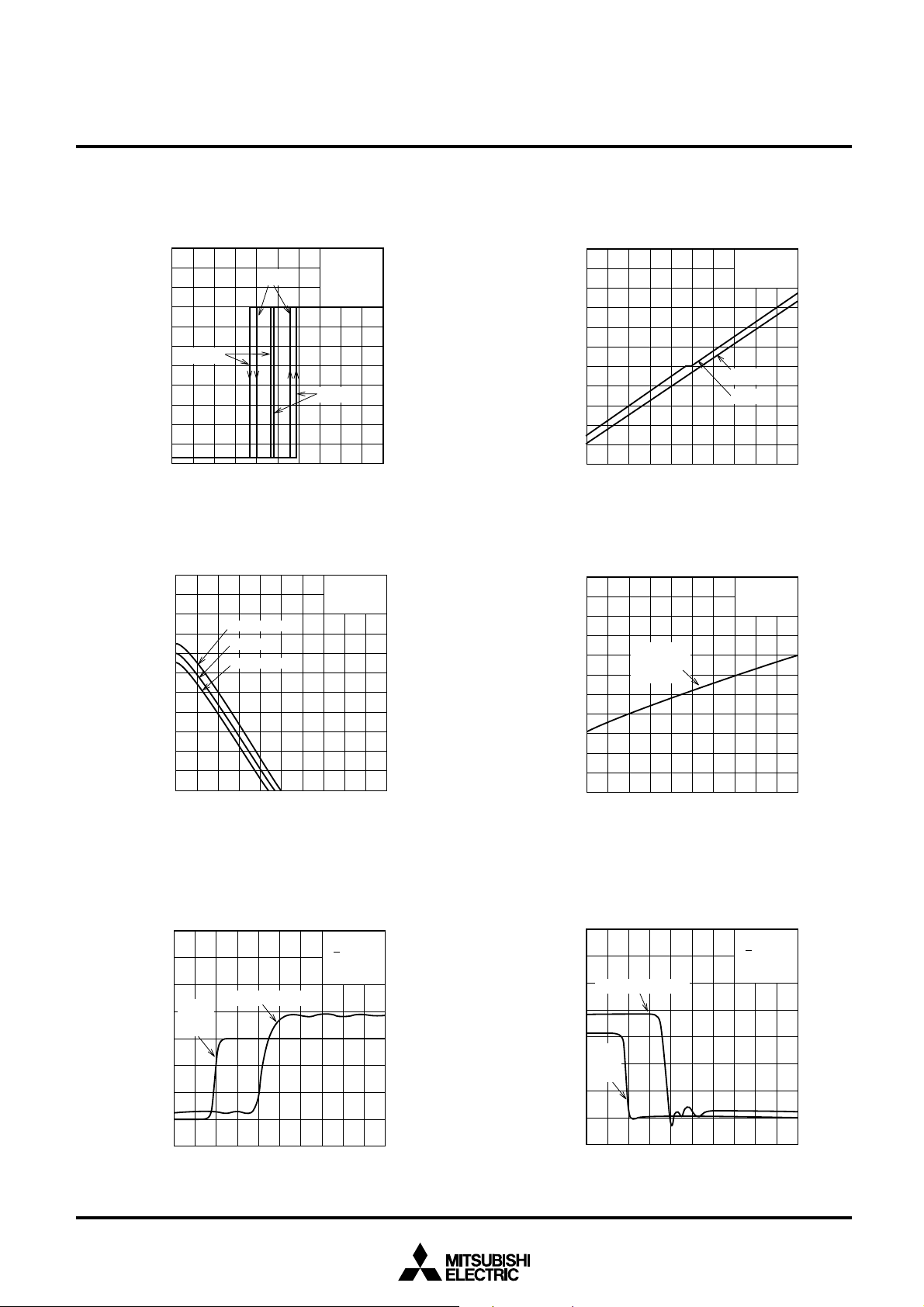
SWITCHING CHARACTERISTIC
Y-Z
6
(V)
INPUT VOLTAGE WAVEFORM
Differential output
voltage waveform
D input
4
voltage
waveform
2
0
0 20406080
DIFFERENTIAL OUTPUT DELAY TIME tDD,
DIFFERENTIAL OUTPUT TRANSITION TIME t
O
(mA)
VCC=5V
T
a
=25°C
TD
(ns)
1
0
“L” OUTPUT VOLTAGE V
1
DIFFERENTIAL OUTPUT VOLTAGE VOD (V)
0
0 20406080100
OUTPUT CURRENT IO (mA)
1
0
IN-PHASE OUTPUT VOLTAGE V
SWITCHING CHARACTERISTIC
(V)
4
2
0
–2
–4
6
(V)
Y output voltage waveform
4
D input
voltage
waveform
2
I/O VOLTAGE WAVEFORM
0
DIFFERENTIAL OUTPUT VOLTAGE WAVEFORM
0 20406080
OUTPUT “L-H” PROPAGATION DELAY TIME t
OUTPUT “H-L” PROPAGATION DELAY TIME t
Z output voltage waveform
VCC=5V
T
a
=25°C
PLH
PHL
,
(ns)
7
MITSUBISHI 〈DIGITAL ASSP〉
M75176P, M75177P
M75178P, M75179P
RS-485 TRANSCEIVER
RECEIVER
I/O TRANSMISSION CHARACTERISTIC (A→R)
VIC=12V
ID
(mV)
VCC=5V
I
O
=0mA
T
a
=25°C
5
(V)
4
O
3
VIC=–7V
2
OUTPUT VOLTAGE V
1
0
–160 –80 0 80 160
INPUT VOLTAGE V
VIC=0V
“H” OUTPUT VOLTAGE - “H” OUTPUT CURRENT CHARACTERISTIC
VID=0.2V
T
a
=25°C
(V)
OH
5
4
3
VCC=5.25V
VCC=5V
VCC=4.75V
INPUT CURRENT - INPUT VOLTAGE CHARACTERISTIC (A)
2.4
1.6
(mA)
I
0.8
0
–0.8
INPUT CURRENT I
–1.6
–20 –10 0 10 20
INPUT VOLTAGE V
B=0V
T
a
=25°C
VCC=5V
VCC=0V
I
(V)
“L” OUTPUT VOLTAGE - “L” OUTPUT CURRENT CHARACTERISTIC
0.5
0.4
0.3
VCC=4.75V
5V
5.75V
VID=–0.2V
T
a=25°C
2
1
“H” OUTPUT VOLTAGE V
0
0 –20 –40 –60 –80 –100
“H” OUTPUT CURRENT I
OH
SWITCHING CHARACTERISTIC
6
(V)
R output voltage waveform
A input
4
voltage
waveform
2
I/O VOLTAGE WAVEFORM
0
0 20406080
OUTPUT “L-H” PROPAGATION DELAY TIME t
(mA)
VCC=5V
B=1.5V
T
a
=25°C
PLH
(ns)
0.2
0.1
“L” OUTPUT VOLTAGE VOL (V)
0
0 4 8 12 16 20
“L” OUTPUT CURRENT IOL (mA)
SWITCHING CHARACTERISTIC
6
(V)
I/O VOLTAGE WAVEFORM
R output voltage waveform
4
A input
voltage
2
waveform
0
0 20406080
OUTPUT “H-L” PROPAGATION DELAY TIME t
VCC=5V
B=1.5V
T
a
=25°C
PHL
(ns)
8

APPLICATION EXAMPLE
MITSUBISHI 〈DIGITAL ASSP〉
M75176P, M75177P
M75178P, M75179P
RS-485 TRANSCEIVER
Data input
Data output
M75176P
R
T
Data output
M75176P
R
T
Data input
M75177P
M75178P
M75176P
Data output
R
T
R
T
Data input
R
T
=Terminal resistor
9
 Loading...