

Mitsubishi M6MGT162S4BVP, M6MGB162S4BVP Datasheet
MITSUBISHI LSIs
M6MGB/T162S4BVP
16,777,216-BIT (1,048,576 -WORD BY 16-BIT ) CMOS
3.3V-ONLY FLASH MEMORY &
4,194,304-BIT (524,288-WORD BY 8-BIT) CMOS SRAM
Stacked-MCP (Multi Chip Package)
DESCRIPTION
The MITSUBISHI M6MGB/T162S4BVP is a Stacked Multi
Chip Package (S-MCP) that contents 16M-bits flash memory
and 4M-bits Static RAM in a 48-pin TSOP (TYPE-I).
16M-bits Flash memory is a 1048576 words, 3.3V-only, and
high performance non-volatile memory fabricated by CMOS
technology for the peripheral circuit and DINOR(DIvided
bit-line NOR) architecture for the memory cell.
4M-bits SRAM is a 262144words unsynchronous SRAM
fabricated by silicon-gate CMOS technology.
M6MGB/T162S4BVP is suitable for the application of the
mobile-communication-system to reduce both the mount
space and weight .
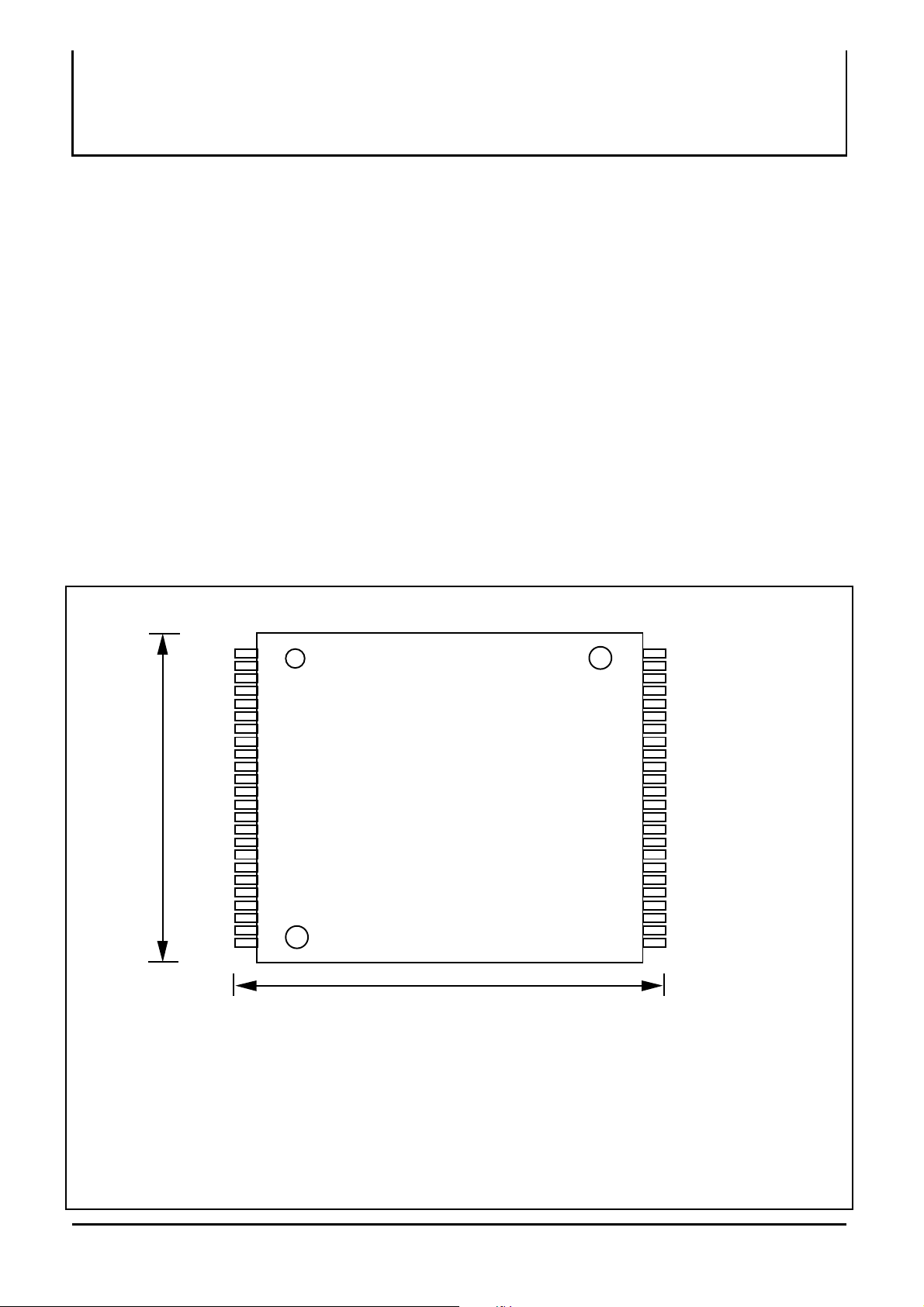
PIN CONFIGURATION (TOP VIEW)
A15
A14
A13
A12
A11
A10
A19
S-CE
WE#
F-RP#
F-WP#
S-VCC
10.0 mm
F-RY/BY#
A18
A17
A7
A6
A5
A4
A3
A2
A1
A9
A8
1
2
3
4
5
6
7
8
9
10
11
12
13
14
15
16
17
18
19
20
21
22
23
24
FEATURES
• Access time
Flash Memory 90ns (Max.)
SRAM 85ns (Max.)
• Supply voltage Vcc=2.7 ~ 3.6V
• Ambient temperature
W version Ta=-20 ~ 85°C
• Package : 48-pin TSOP (Type-I) , 0.4mm lead pitch
APPLICATION
Mobile communication products
48
47
46
45
44
43
42
41
40
39
38
37
36
35
34
33
32
31
30
29
28
27
26
25
A16
DQ15
GND
S-A-1
DQ7
DQ14
DQ6
DQ13
DQ5
DQ12
DQ4
F-VCC
DQ11
DQ3
DQ10
DQ2
DQ9
DQ1
DQ8
DQ0
OE#
GND
F-CE#
A0
14.0 mm
F-VCC
S-VCC
GND :GND for Flash SRAM
S-A-1
A0-A17
A18-A19 :Address for Flash
DQ0-DQ15
F-CE# :Flash Chip Enable
S-CE :SRAM Chip Enable
OE#
WE#
F-WP# :Flash Write Protect
F-RP# :Flash Reset Power Down
F-RY/BY# :Flash Ready /Busy
1
:Vcc for Flash
:Vcc for SRAM
:Address for SRAM
:Flash/SRAM common Address
:Data I/O
:Flash/SRAM Output Enable
:Flash/SRAM Write Enable
NC:Non Connection
Sep. 1999 , Rev.2.0
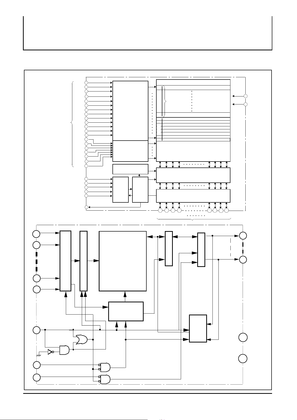
BLOCK DIAGRAM
MITSUBISHI LSIs
M6MGB/T162S4BVP
16,777,216-BIT (1,048,576 -WORD BY 16-BIT ) CMOS
3.3V-ONLY FLASH MEMORY &
4,194,304-BIT (524,288-WORD BY 8-BIT) CMOS SRAM
Stacked-MCP (Multi Chip Package)
16Mb Flash Memory
ADDRESS
INPUTS
CHIP ENABLE INPUT
OUTPUT ENABLE INPUT
WRITE ENABLE INPUT
WRITE PROTECT INPUT
RESET/POWER DOWN INPUT
READY/BUSY OUTPUT
F-RY/BY#
4Mb SRAM
S-A-1
A19
A18
A17
A16
A15
A14
A13
A12
A11
A10
A9
A8
A7
A6
A5
A4
A3
A2
A1
A0
F-CE#
OE#
WE#
F-WP#
F-RP#
X-DECODER
Y-DECODER
STATUS / ID REGISTER
WSM
CUI
WSM
128 WORD PAGE BUFFER
Main Block 32KW
Bank(II)
28
Main Block 32KW
Parameter Block7 16KW
Bank(I)
DQ15DQ14DQ13DQ12 DQ2DQ1DQ0DQ3
Parameter Block6 16KW
Parameter Block5 16KW
Parameter Block4 16KW
Parameter Block3 16KW
Parameter Block2 16KW
Parameter Block1 16KW
Boot Block 16KW
Y-GATE / SENSE AMP.
MULTIPLEXER
INPUT/OUTPUT
BUFFERS
DATA INPUTS/OUTPUTS
F-VCC(3.3V)
GND (0V)
DQ0
A0
A16
A17
S-CE
WE#
OE#
524288 WORD x
8 BITS
ROW DECODER
ADDRESS INPUT BUFFER
GENERATOR
CLOCK
SENSE AMP.
DATAINPUT
DQ7
OUTPUT BUFFER
S-VCC
BUFFER
GND
2
Sep. 1999 , Rev.2.0

MITSUBISHI LSIs
M6MGB/T162S4BVP
16,777,216-BIT (1,048,576 -WORD BY 16-BIT ) CMOS
3.3V-ONLY FLASH MEMORY &
4,194,304-BIT (524,288-WORD BY 8-BIT) CMOS SRAM
Stacked-MCP (Multi Chip Package)
1. Flash Memory
DESCRIPTION
The Flash Memory of M6MGB/T162S4BVP is 3.3V-only high speed 16,777,216-bit CMOS boot block Flash Memories with alternating
BGO (Back Ground Operation) feature. The BGO feature of the device allows Program or Erase operations to be performed in one bank
while the device simultaneously allows Read operations to be performed on the other bank. This BGO feature is suitable for mobile and
personal computing, and communication products. The Flash Memory of M6MGB/T162S4BVP is fabricated by CMOS technology for the
peripheral circuits and DINOR(Divided bit line NOR) architecture for the memory cells.
FEATURES
Organization 1048,576 word x 16bit
Supply voltage
Access time 90ns (Max.)
Power Dissipation
Read 54 mW (Max. at 5MHz)
(After Automatic Power saving) 0.33mW (typ.)
Program/Erase 126 mW (Max.)
Standby 0.33mW (typ.)
Deep power down mode 0.33mW (typ.)
Auto program for Bank(I)
Program Time 4ms (typ.)
Program Unit
(Byte Program) 1word
(Page Program) 128word
Auto program for Bank(II)
Program Time 4ms (typ.)
Program Unit 128word
Auto Erase
Erase time 40 ms (typ.)
Erase Unit
Bank(I) Boot Block 16Kword x 1
Parameter Block 16Kword x 7
Bank(II) Main Block 32Kword x 28
Program/Erase cycles 100Kcycles
.................................
.............................
................................ VCC = 2.7~3.6V
..............................
.................................
..........
.................................
.................................
.......................
.................................
.........................
.........................
.................................
.................................
.................................
.....................
..............
......................
.........................................
Boot Block
M6MGB162S4BVP Bottom Boot
M6MGT162S4BVP Top Boot
Other Functions
Soft Ware Command Control
Selective Block Lock
Erase Suspend/Resume
Program Suspend/Resume
Status Register Read
Alternating Back Ground Program/Erase Operation
Between Bank(I) and Bank(II)
........................
........................
3
Sep. 1999 , Rev.2.0

MITSUBISHI LSIs
M6MGB/T162S4BVP
16,777,216-BIT (1,048,576 -WORD BY 16-BIT ) CMOS
3.3V-ONLY FLASH MEMORY &
4,194,304-BIT (524,288-WORD BY 8-BIT) CMOS SRAM
Stacked-MCP (Multi Chip Package)
FUNCTION
The Flash Memory of M6MGB/T162S4BVP includes on-chip
program/erase control circuitry. The Write State Machine (WSM)
controls block erase and byte/page program operations.
Operational modes are selected by the commands written to the
Command User Interface (CUI). The Status Register indicates the
status of the WSM and when the WSM successfully completes the
desired program or block erase operation.
A Deep Powerdown mode is enabled when the F-RP# pin is at
GND, minimizing power consumption.
Read
The Flash Memory of M6MGB/T162S4BVP has three read modes,
which accesses to the memory array, the Device Identifier and the
Status Register. The appropriate read command are required to
be written to the CUI. Upon initial device powerup or after exit
from deep powerdown, the Flash Memory automatically resets to
read array mode. In the read array mode, low level input to F-CE#
and OE#, high level input to WE# and F-RP#, and address signals
to the address inputs ( A19-A0:Word Mode) output the data of the
addressed location to the data input/output ( D15-D0:Word Mode).
Write
Writes to the CUI enables reading of memory array data, device
identifiers and reading and clearing of the Status Register. They
also enable block erase and program. The CUI is written by
bringing WE# to low level, while F-CE# is at low level and OE# is
at high level. Address and data are latched on the earlier rising
edge of WE# and F-CE#. Standard micro-processor write timings
are used.
Deep Power-Down
When F-RP# is at VIL, the device is in the deep powerdown
mode and its power consumption is substantially low. During
read modes, the memory is deselected and the data
input/output are in a high-impedance(High-Z) state. After
return from powerdown, the CUI is reset to Read Array , and
the Status Register is cleared to value 80H.
During block erase or program modes, F-RP# low will abort
either operation. Memory array data of the block being altered
become invalid.
Automatic Power-Saving (APS)
The Automatic Power-Saving minimizes the power
consumption during read mode. The device automatically
turns to this mode when any addresses or F-CE# isn't
changed more than 200ns after the last alternation. The
power consumption becomes the same as the stand-by
mode. While in this mode, the output data is latched and can
be read out. New data is read out correctly when addresses
are changed.
Alternating Background Operation (BGO)
The Flash Memory of M6MGB/T162S4BVP allows to read array
from one bank while the other bank operates in software
command write cycling or the erasing / programming operation in
the background. Read array operation with the other bank in BGO
is performed by changing the bank address without any additional
command. When the bank address points the bank in software
command write cycling or the erasing / programming operation,
the data is read out from the status register. The access time with
BGO is the same as the normal read operation.
Output Disable
When OE# is at VIH, output from the devices is disabled. Data
input/output are in a high-impedance(High-Z) state.
Standby
When F-CE# is at VIH, the device is in the standby mode and
its power consumption is reduced. Data input/output are in a
high-impedance(High-Z) state. If the memory is deselected
during block erase or program, the internal control circuits
remain active and the device consume normal active power
until the operation completes.
4
Sep. 1999 , Rev.2.0

MITSUBISHI LSIs
M6MGB/T162S4BVP
16,777,216-BIT (1,048,576 -WORD BY 16-BIT ) CMOS
3.3V-ONLY FLASH MEMORY &
4,194,304-BIT (524,288-WORD BY 8-BIT) CMOS SRAM
Stacked-MCP (Multi Chip Package)
SOFTWARE COMMAND DEFINITIONS
The device operations are selected by writing specific software
command into the Command User Interface.
Read Array Command (FFH)
The device is in Read Array mode on initial device power up and
after exit from deep powerdown, or by writing FFH to the
Command User Interface. After starting the internal operation the
device is set to the read status register mode automatically.
Read Device Identifier Command (90H)
It can normally read device identifier codes when Read Device
Identifier Code Command(90H) is written to the command latch.
Following the command write, the manufacturer code and the
device code can be read from address 0000H and 0001H,
respectively.
Read Status Register Command (70H)
The Status Register is read after writing the Read Status Register
command of 70H to the Command User Interface. Also, after
starting the internal operation the device is set to the Read Status
Register mode automatically.
The contents of Status Register are latched on the later falling
edge of OE# or F-CE#. So F-CE# or OE# must be toggled every
status read.
Clear Status Register Command (50H)
The Erase Status, Program Status and Block Status bits are set to
"1"s by the Write State Machine and can only be reset by the Clear
Status Register command of 50H. These bits indicates various
failure conditions.
C)Single Data Load to Page Buffer (74H)
/ Page Buffer to Flash (0EH/D0H)
Single data load to the page buffer is performed by writing 74H
followed by a second write specifying the column address and
data. Distinct data up to 128word can be loaded to the page
buffer by this two-command sequence. On the other hand, all of
the loaded data to the page buffer is programed simultaneously
by writing Page Buffer to Flash command of 0EH followed by the
confirm command of D0H. After completion of programing the
data on the page buffer is cleared automatically.
This command is valid for only Bank(I) alike Word Program.
Clear Page Buffer Command (55H)
Loaded data to the page buffer is cleared by writing the Clear
Page Buffer command of 55H followed by the Confirm command
of D0H. This command is valid for clearing data loaded by Single
Data Load to Page Buffer command.
Suspend/Resume Command (B0H/D0H)
Writing the Suspend command of B0H during block erase
operation interrupts the block erase operation and allows read out
from another block of memory. Writing the Suspend command of
B0H during program operation interrupts the program operation
and allows read out from another block of memory. The Bank
address is required when writing the Suspend/Resume Command.
The device continues to output Status Register data when read,
after the Suspend command is written to it. Polling the WSM
Status and Suspend Status bits will determine when the erase
operation or program operation has been suspended. At this
point, writing of the Read Array command to the CUI enables
reading data from blocks other than that which is suspended.
When the Resume command of D0H is written to the CUI,
the WSM will continue with the erase or program processes.
Block Erase / Confirm Command (20H/D0H)
Automated block erase is initiated by writing the Block Erase
command of 20H followed by the Confirm command of D0H. An
address within the block to be erased is required. The WSM
executes iterative erase pulse application and erase verify
operation.
Program Commands
A)Word/Byte Program (40H)
Word program is executed by a two-command sequence. The
Word Program Setup command of 40H is written to the
Command Interface, followed by a second write specifying the
address and data to be written. The WSM controls the program
pulse application and verify operation. The Word Program
Command is Valid for only Bank(I).
B)Page Program for Data Blocks (41H)
Page Program for Bank(I) and Bank(II) allows fast programming of
128words/256bytes of data. Writing of 41H initiates the page
program operation for the Data area. From 2nd cycle to
129th cycle, write data must be serially inputted. Address A6-A0
have to be incremented from 00H to 7FH. After completion of data
loading, the WSM controls the program pulse application and verify
operation.
DATA PROTECTION
The Flash Memory of M6MGB/T162S4BVP provides selectable
block locking of memory blocks. Each block has an associated
nonvolatile lock-bit which determines the lock status of the block.
In addition, the Flash Memory has a master Write Protect pin
(F-WP#) which prevents any modifications to memory blocks
whose lock-bits are set to "0", when F-WP# is low. When F-WP#
is high, all blocks can be programmed or erased regardless of
the state of the lock-bits, and the lock-bits are cleared to "1" by
erase. See the BLOCK LOCKING table on P.9 for details.
Power Supply Voltage
When the power supply voltage (F-VCC) is less than V
V
CC Lock-Out voltage, the device is set to the Read-only mode.
Regarding DC electrical characteristics of V
A delay time of 2 us is required before any device operation is
initiated. The delay time is measured from the time F-Vcc reaches
F-Vccmin (2.7V).
During power up, F-RP#=GND is recommended. Falling in Busy
status is not recommended for possibility of damaging the device.
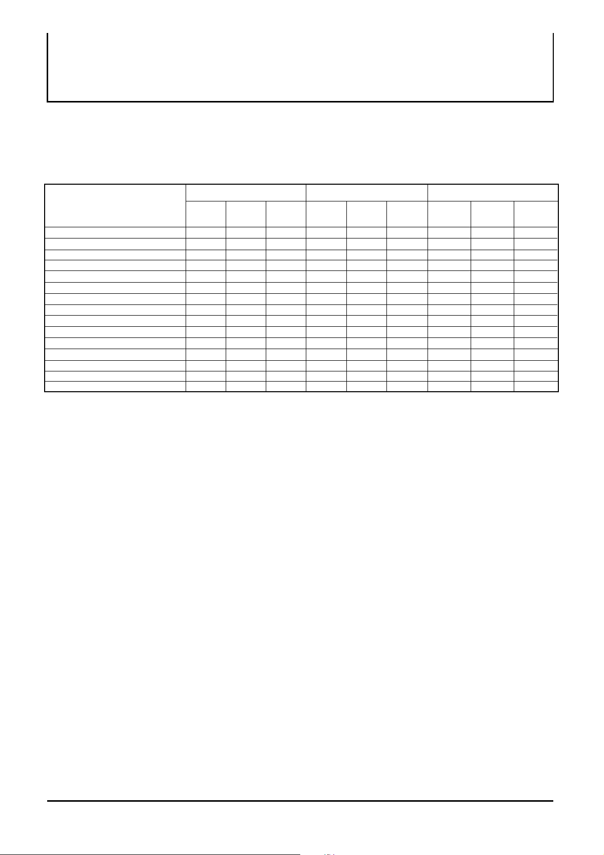
MEMORY ORGANIZATION
The Flash Memory of M6MGB/T162S4BVP has one 16Kword boot
block, seven 16Kword parameter blocks, for Bank(I) and
twenty-eight 32Kword main blocks for Bank(II). A block is erased
independently of other blocks in the array.
LKO, see P.10.
LKO, Low
5
Sep. 1999 , Rev.2.0
MEMORY ORGANIZATION
MITSUBISHI LSIs
M6MGB/T162S4BVP
16,777,216-BIT (1,048,576 -WORD BY 16-BIT ) CMOS
3.3V-ONLY FLASH MEMORY &
4,194,304-BIT (524,288-WORD BY 8-BIT) CMOS SRAM
Stacked-MCP (Multi Chip Package)
x16 ( Wordmode)
F8000H-FFFFFH
F0000H-F7FFFH
E8000H-EFFFFH
E0000H-E7FFFH
D8000H-DFFFFH
D0000H-D7FFFH
C8000H-CFFFFH
C0000H-C7FFFH
B8000H-BFFFFH
B0000H-B7FFFH
A8000H-AFFFFH
A0000H-A7FFFH
98000H-9FFFFH
90000H-97FFFH
88000H-8FFFFH
80000H-87FFFH
78000H-7FFFFH
70000H-77FFFH
68000H-6FFFFH
60000H-67FFFH
58000H-5FFFFH
50000H-57FFFH
48000H-4FFFFH
40000H-47FFFH
38000H-3FFFFH
30000H-37FFFH
28000H-2FFFFH
20000H-27FFFH
1C000H-1FFFFH
18000H-1BFFFH
14000H-17FFFH
10000H-13FFFH
0C000H-0FFFFH
08000H-0BFFFH
04000H-07FFFH
00000H-03FFFH
A19-A0
(Word Mode)
32Kword MAIN BLOCK 35
32Kword MAIN BLOCK 34
32Kword MAIN BLOCK 33
32Kword MAIN BLOCK 32
32Kword MAIN BLOCK 31
32Kword MAIN BLOCK 30
32Kword MAIN BLOCK 29
32Kword MAIN BLOCK 28
32Kword MAIN BLOCK 27
32Kword MAIN BLOCK 26
32Kword MAIN BLOCK 25
32Kword MAIN BLOCK 24
32Kword MAIN BLOCK 23
32Kword MAIN BLOCK 22
32Kword MAIN BLOCK 21
32Kword MAIN BLOCK 20
32Kword MAIN BLOCK 19
32Kword MAIN BLOCK 18
32Kword MAIN BLOCK 17
32Kword MAIN BLOCK 16
32Kword MAIN BLOCK 15
32Kword MAIN BLOCK 14
32Kword MAIN BLOCK 13
32Kword MAIN BLOCK 12
32Kword MAIN BLOCK 11
32Kword MAIN BLOCK 10
32Kword MAIN BLOCK 9
32Kword MAIN BLOCK 8
16Kword PARAMETER BLOCK 7
16Kword PARAMETER BLOCK 6
16Kword PARAMETER BLOCK 5
16Kword PARAMETER BLOCK 4
16Kword PARAMETER BLOCK 3
16Kword PARAMETER BLOCK 2
16Kword PARAMETER BLOCK 1
16Kword BOOT BLOCK 0
Flash Memory of M6MGB162S4BVP
Memory Map
BANK(II)
BANK(I)
x16 ( Wordmode)
FC000H-FFFFFH
F8000H-FBFFFH
F4000H-F7FFFH
F0000H-F3FFFH
EC000H-EFFFFH
E8000H-EBFFFH
E4000H-E7FFFH
E0000H-E3FFFH
D8000H-DFFFFH
D0000H-D7FFFH
C8000H-CFFFFH
C0000H-C7FFFH
B8000H-BFFFFH
B0000H-B7FFFH
A8000H-AFFFFH
A0000H-A7FFFH
98000H-9FFFFH
90000H-97FFFH
88000H-8FFFFH
80000H-87FFFH
78000H-7FFFFH
70000H-77FFFH
68000H-6FFFFH
60000H-67FFFH
58000H-5FFFFH
50000H-57FFFH
48000H-4FFFFH
40000H-47FFFH
38000H-3FFFFH
30000H-37FFFH
28000H-2FFFFH
20000H-27FFFH
18000H-1FFFFH
10000H-17FFFH
08000H-0FFFFH
00000H-07FFFH
A19-A0
(Word Mode)
16Kword BOOT BLOCK 35
16Kword PARAMETER BLOCK 34
16Kword PARAMETER BLOCK 33
16Kword PARAMETER BLOCK 32
16Kword PARAMETER BLOCK 31
16Kword PARAMETER BLOCK 30
16Kword PARAMETER BLOCK 29
16Kword PARAMETER BLOCK 28
32Kword MAIN BLOCK 27
32Kword MAIN BLOCK 26
32Kword MAIN BLOCK 25
32Kword MAIN BLOCK 24
32Kword MAIN BLOCK 23
32Kword MAIN BLOCK 22
32Kword MAIN BLOCK 21
32Kword MAIN BLOCK 20
32Kword MAIN BLOCK 19
32Kword MAIN BLOCK 18
32Kword MAIN BLOCK 17
32Kword MAIN BLOCK 16
32Kword MAIN BLOCK 15
32Kword MAIN BLOCK 14
32Kword MAIN BLOCK 13
32Kword MAIN BLOCK 12
32Kword MAIN BLOCK 11
32Kword MAIN BLOCK 10
32Kword MAIN BLOCK 9
32Kword MAIN BLOCK 8
32Kword MAIN BLOCK 7
32Kword MAIN BLOCK 6
32Kword MAIN BLOCK 5
32Kword MAIN BLOCK 4
32Kword MAIN BLOCK 3
32Kword MAIN BLOCK 2
32Kword MAIN BLOCK 1
32Kword MAIN BLOCK 0
Flash Memory of M6MGT162S4BVP
Memory Map
BANK(I)
BANK(II)
6
Sep. 1999 , Rev.2.0
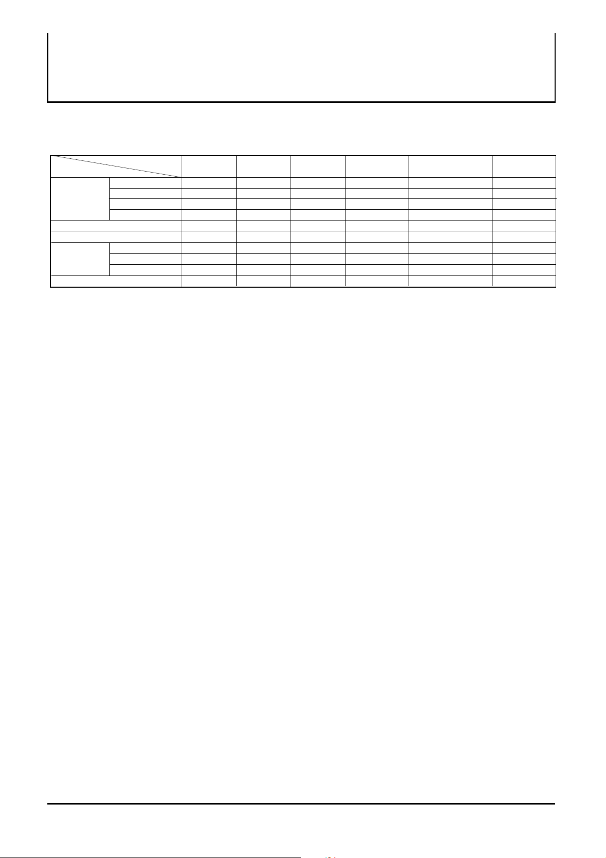
BUS OPERATIONS
Bus Operations for Word-Wide Mode
MITSUBISHI LSIs
M6MGB/T162S4BVP
16,777,216-BIT (1,048,576 -WORD BY 16-BIT ) CMOS
3.3V-ONLY FLASH MEMORY &
4,194,304-BIT (524,288-WORD BY 8-BIT) CMOS SRAM
Stacked-MCP (Multi Chip Package)
Mode
Pins
Array
Read
Status Register
Lock Bit Status VIL VIL
Identifier Code
Output disable
Stand by
Program
Write
Erase
Others
Deep Power Down
1) X at F-RY/BY# is VOL or VOH(Hi-Z).
*The F-RY/BY# is an open drain output pin and indicates status of the internal WSM. When low,it indicates that the WSM is Busy performing an operation.
A pull-up resistor of 10K-100K Ohms is required to allow the F-RY/BY# signal to transition high indicating a Ready WSM condition.
2) X can be V
IH or VIL for control pins.
F-CE# OE# WE#
V
IL
VIL
VIL
VIL
VIH
VIH
VIH
VIL
VIL
VIH
VIL
VIL
V
IL VIH
X
VIL
VIH
V
VIH
VIH
VIH
2)
X
IH
X
V
VIL
V
X
X Hi-Z
DQ
F-RP#
IH
V
VIH
VIH
Status Register Data
Lock Bit Data (DQ6)X
VIH
VIH
VIH
IL
VIH
Command/Data in
VIH
IH
IL
V
0-15
Data out
Identifier Code
Hi-Z
Hi-Z
Command
VIL
F-RY/BY#
OH (Hi-Z)
V
X
V
OH (Hi-Z)
X
X
X
X
XCommand
VOH (Hi-Z)
1)
7
Sep. 1999 , Rev.2.0
SOFTWARE COMMAND DEFINITION
Command List
MITSUBISHI LSIs
M6MGB/T162S4BVP
16,777,216-BIT (1,048,576 -WORD BY 16-BIT ) CMOS
3.3V-ONLY FLASH MEMORY &
4,194,304-BIT (524,288-WORD BY 8-BIT) CMOS SRAM
Stacked-MCP (Multi Chip Package)
1st bus cycle
Command
Mode
Address
Read Array
Device Identifier
Read Status Register
Write
Bank
Clear Status Register
Clear Page Buffer
Word Program
Page Program
Single Data Load to Page Buffer
Page Buffer to Flash
Block Erase / Confirm
Suspend
Resume
Read Lock Bit Status
Lock Bit Program / Confirm
Erase All Unlocked Blocks
1) In the word-wide version, upper byte data (DQ8-DQ15) is ignored.
2) IA=ID Code Address : A0=VIL (Manufacturer's Code) : A0=VIH (Device Code), ID=ID Code
3) Bank = Bank Address (Bank(I) or Bank(II)) : A19-A17.
4) SRD = Status Register Data
5) Word Program, Single Data Load and Page Buffer to Flash Command is valid for only Bank(I).
6) WA = Write Address,WD = Write Data
7) WA0,WAn=Write Address, WD0,WDn=Write Data.
Write Address and Write Data must be provided sequentially from 00H to 7FH for A6-A0. Page size is 128word (128word x 16bit).
and also A19-A7(Block Address, Page Address) must be valid.
8) WA = Write Address : Upper page address, A19-A7(Block Address, Page Address) must be valid.
9) BA = Block Address : BA = Block Address : A19-A14(Bank1) A19-A15(Bank2)
10) DQ6 provides Block Lock Status, DQ6 = 1 : Block Unlock, DQ6 = 0 : Block Locked.
5)
7)
5)
Write 40H Write
Write 41H
5)
Write
Write
Write
Write
Write
Write
Write
Write
Bank(I)
Bank
Bank(I)
Bank(I)
Bank
Bank
Bank
Bank
Data
(DQ15-0)
FFHXWrite
90HX
3)
70HWrite
XWrite
XWrite
50H
55H
5)
5)
74H
5)
0EH
20H
B0H
D0H
X
71H
77H
X
A7H
2nd bus cycle
AddressMode
IARead
Bank
Data
(DQ15-0)
2)
ID
SRDRead
Write X D0H
6)
WD
7)
WD0
WDWA
8)
D0H
9)
D0H
DQ6
D0H
Write
Write
Write
Write
Read
Write
Write
WA
WA
BA
BA
BA
XD0H
3rd ~129th bus cycles (Word Mode)
AddressMode
2)
4)
1)
6)
7)
1)
1)
10)
1)
1)
WAnWA0
Data
(DQ15-0)
7)
7)
WDnWrite
8
Sep. 1999 , Rev.2.0
MITSUBISHI LSIs
M6MGB/T162S4BVP
16,777,216-BIT (1,048,576 -WORD BY 16-BIT ) CMOS
3.3V-ONLY FLASH MEMORY &
4,194,304-BIT (524,288-WORD BY 8-BIT) CMOS SRAM
Stacked-MCP (Multi Chip Package)
BLOCK LOCKING
Lock
F-WP#
F-RP#
VIL
VIH
1) DQ6 provides Lock Status of each block after writing the Read Lock Status command (71H).
WP# pins must not be switched during performing Erase / Write operations or WSM Busy (WSMS = 0).
2) Erase/Write command for locked blocks is aborted. At this time read mode is not array read mode but status read mode and
00B0H is read. Please issue Clear Status Register command plus Read Array command to change the mode from status read mode
to array read mode.
X
VIL
VIH
Bit
(Internally)
X
0
1
X
Unlocked Unlocked Unlocked Unlocked
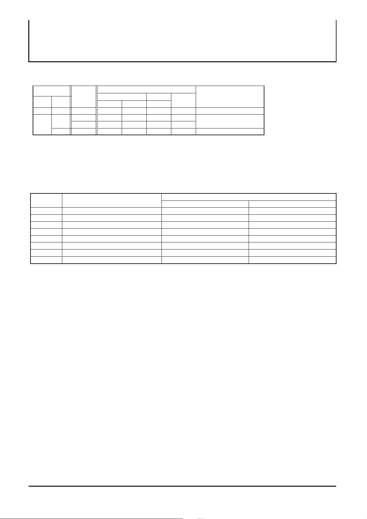
STATUS REGISTER
Symbol
SR.7
SR.6
SR.5
SR.4
SR.3
SR.2
SR.1
SR.0
*The F-RY/BY# is an open drain output pin and indicates status of the internal WSM. When low,it indicates that the WSM is Busy performing an operation.
A pull-up resistor of 10K-100K Ohms is required to allow the F-RY/BY# signal to transition high indicating a Ready WSM condition.
*DQ3 indicates the block status after the page programming, word programming and page buffer to flash. When DQ3 is "1", the page has the over-programed
cell . If over-program occurs, the device is block fail. However if DQ3 is "1", please try the block erase to the block. The block may revive.
(DQ
(DQ
(DQ5)
(DQ
(DQ
(DQ
(DQ1)
(DQ
7)
6)
4)
3)
2)
0)
Status
Write State Machine Status
Suspend Status
Erase Status
Program Status
Block Status after Program
Reserved
Reserved
Reserved
Write Protection Provided
BANK(I)
Boot Parameter Data
Locked
Locked
Locked
Locked Locked Locked
Locked Locked Locked
Unlocked Unlocked
BANK(II)
Lock Bit
Locked
Note
Deep Power Down Mode
All Blocks Unlocked
Definition
"1" "0"
Ready Busy
Suspended Operation in Progress / Completed
Error Successful
Error Successful
Error Successful
--
--
-
-
9
Sep. 1999 , Rev.2.0
 Loading...