Mitsubishi M5M5V4R04J-15, M5M5V4R04J-12 Datasheet

4194304-BIT (1048576-WORD BY 4-BIT) CMOS STATIC RAM
DESCRIPTION
The M5M5V4R04J is a family of 1048576-word by 4-bit static
RAMs, fabricated with the high performance CMOS silicon gate
process and designed for high speed application.
The M5M5V4R04J is offered in a 32-pin plastic small outline Jlead package(SOJ).
These device operate on a single 3.3V supply, and are directly
TTL compatible. They include a power down feature as well.
FEATURES
• Fast access time M5M5V4R04J-12 •••• 12ns(max)
M5M5V4R04J-15 •••• 15ns(max)
• Low power dissipation Active
Stand by ••••••• 3.3mW(typ)
• Single +3.3V power supply
• Fully static operation : No clocks, No refresh
• Common data I/O
• Easy memory expansion by S
• Three-state outputs : OR-tie capability
• OE prevents data contention in the I/O bus
• Directly TTL compatible : All inputs and outputs
•••••••••• 297mW(typ)
M5M5V4R04J-12,-15
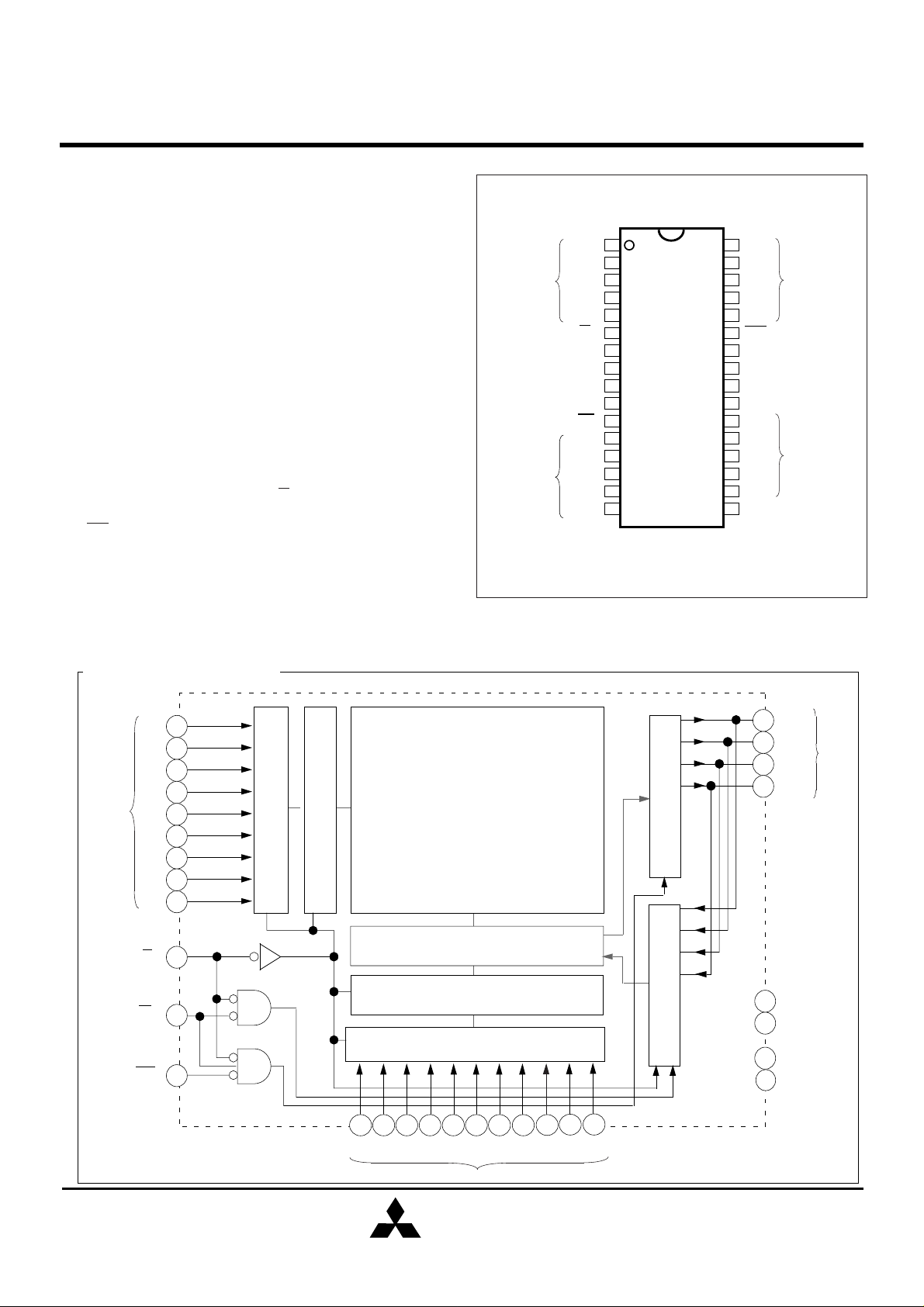
PIN CONFIGURATION (TOP VIEW)
1
A0
2
(0V)
A1
3
A2
4
A3
5
A4
6
S
7
DQ1
8
VCC
9
GND
10
DQ2
11
W
12
A5
13
A6
14
A
7
15
A8
16
9
A
Outline 32P0K(SOJ)
M5M5V4R04J
address
inputs
chip select
input
datainputs/
outputs
(3.3V)
datainputs/
outputs
write control
input
address
inputs
MITSUBISHI LSIs
1997.11.20 Rev.F
32
A19
31
A
18
30
29
28
27
OE
26
25
24
23
22
21
20
19
18
17
A17
16
A
15
A
output enable
input
DQ4
(0V)
GND
(3.3V)
VCC
DQ3
A14
A
13
A12
A11
A10
NC
address
inputs
data inputs/
outputs
datainputs/
outputs
address
inputs
APPLICATION
High-speed memory units
BLOCK DIAGRAM
A0
1
A1
2
A2
3
A3
address
inputs
A4
A
5
12
A6
13
A7
14
A8
15
S
W
11
OE 27
4
5
ROW INPUT BUFFERS
6
MEMORY ARRAY
512 ROWS
8192 COLUMNS
ROW ADDRESS DECODERS
COLUMN I/O CIRCUITS
COLUMN ADDRESS
COLUMN
DECODERS
ADDRESS
DECODERS
COLUMN INPUT BUFFERS
PACKAGE
32pin 400mil SOJ
DQ1
7
DQ2
10
DQ3
23
DQ4
26
OUTPUT BUFFERS
8
VCC
24
DATA INPUT BUFFERS
25
9
GND
data
inputs/
outputs
(3.3V)
(0V)
18 19
address inputs
20 21 221628 29
MITSUBISHI
ELECTRIC
A16A15A14A13A12A11A10A9
31
A1730A18
32
A19
1

4194304-BIT (1048576-WORD BY 4-BIT) CMOS STATIC RAM
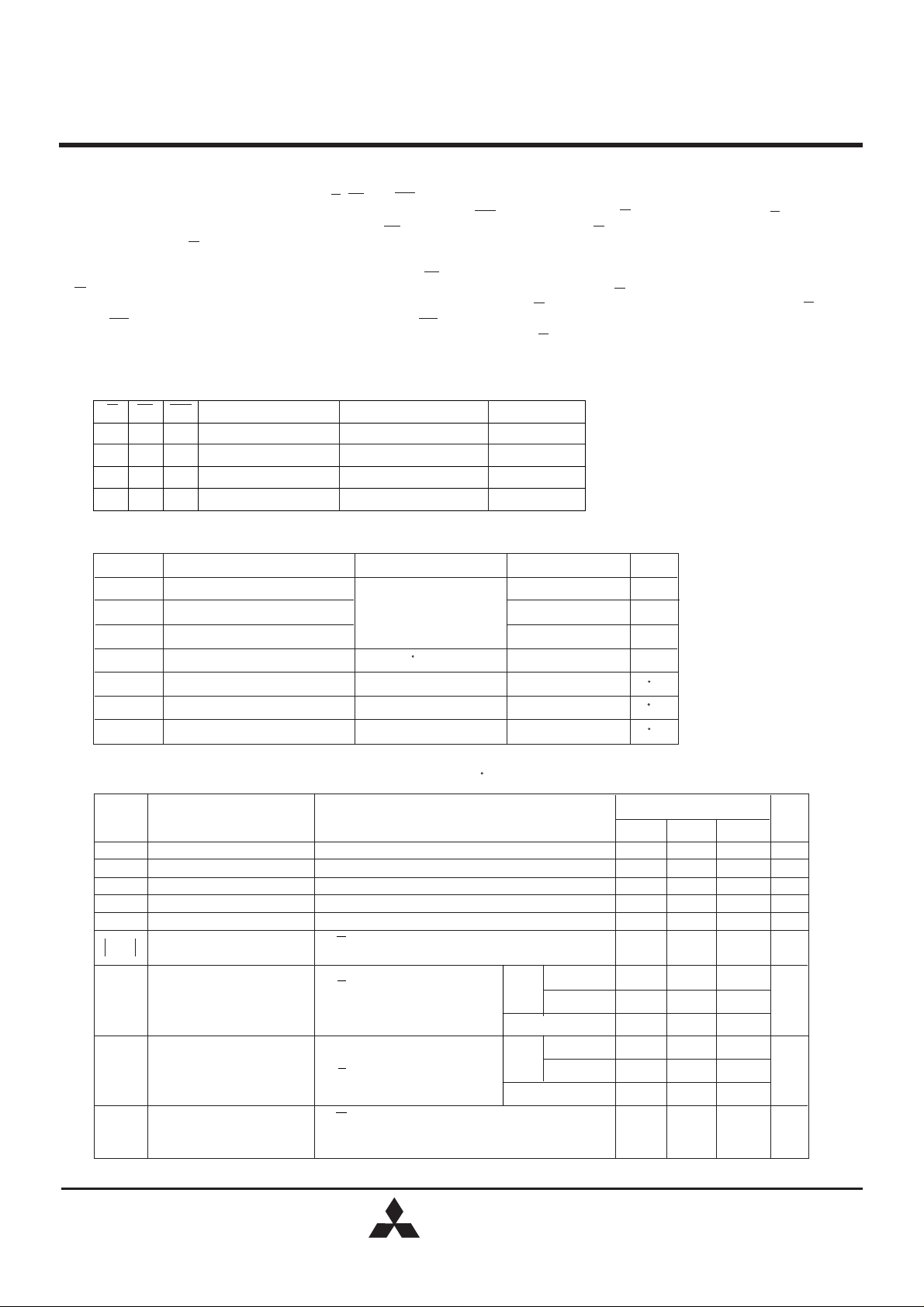
FUNCTION
The operation mode of the M5M5V4R04J is determined by a
combination of the device control inputs S, W and OE. Each
mode is summarized in the function table.
A write cycle is executed whenever the low level W overlaps
with the low level S. The address must be set-up before the
write cycle and must be stable during the entire cycle.
The data is latched into a cell on the trailing edge of W or
S, whichever occurs first, requiring the set-up and hold time
relative to these edge to be maintained. The output enable
input OE directly controls the output stage. Setting the OE at
a high level, the output stage is in a high impedance state,
and the data bus
FUNCTION TABLE
MITSUBISHI LSIs
M5M5V4R04J-12,-15
contention problem in the write cycle is eliminated.
A read cycle is excuted by setting W at a high level and
OE at a low level while S are in an active state (S=L).
When setting S at high level, the chip is in a nonselectable mode in which both reading and writing are
disable. In this mode, the output stage is in a highimpedance state, allowing OR-tie with other chips and
memory expansion by S.
Signal-S controls the power-down feature. When S goes
high, power dissapation is reduced extremely. The access
time from S is equivalent to the address access time.
S
H
W OE
XX
Mode
Non selection Stand by
High-impedance
L Write ActiveDinLX
L Read
L ActiveHigh-impedance
HH
DoutHL
ABSOLUTE MAXIMUM RATINGS
Symbol
V
cc
VI
V
O
Pd
Topr
Tstg(bias)
T
stg
*Pulse width ≤ 20ns, In case of DC:-0.5V
Parameter
Supply voltage
Input voltage
Output voltage
Power dissipation
Operating temperature
Storage temperature
Storage temperature
With respect to GND
Ta=25 C
(bias)
DC ELECTRICAL CHARACTERISTICS
Symbol Parameter
V
IH
High-level input voltage
V
IL
Low-level input voltage
VOH
High-level output voltage
VOL 0.4
Low-level output voltage
Input current
I
I
Output current in off-state
I
OZ
I
I
I
Active supply current
CC1
(TTL level)
Stand by current
CC2
(TTL level)
Stand by current
CC3
I
OH =-4mA
OL= 8mA
I
V
= 0~Vcc
I
VI (S)= VIH
VO= 0~Vcc
I (S)= VIL
V
other inputs VIH or VIL
Output-open(duty 100%)
VI (S)= VIH
VI (S)= Vcc≥0.2V
other inputs V
or V
I≥Vcc-0.2V
DQ
Icc
Active
Ratings
*
-2.0 ~ 4.6
*
-2.0 ~ VCC+0.5
*
-2.0 ~ VCC+0.5
1000
0 ~ 70
-10 ~ 85
-65 ~ 150
(Ta=0 ~ 70 C, Vcc=3.3V unless otherwise noted)
+10%
-5%
Condition
UnitConditions
V
V
V
mW
C
C
C
Limits
Min
2.0
-0.3
2.4
12ns cycle
AC
15ns cycle
DC
90
12ns cycle
AC
15ns cycle
DC
I≤0.2V
1
MaxTyp
Vcc+0.3
0.8
2
10
160
150
100
75
70
50
10
Unit
V
V
V
V
µA
µA
mA
mA
mA
MITSUBISHI
ELECTRIC
2
 Loading...