

address
PRELIMINARY
1998.11.30 Ver.B
The M5M54R04AJ is a family of 1048576-word by 4-bit
static RAMs, fabricated with the high performance CMOS
silicon gate process and designed for high speed
application.
These devices operate on a single 3.3V supply, and are
directly TTL compatible. They include a power down
feature as well.
123456789101112131415
16
32313029282726252423222120
19
18
17
address
address
address
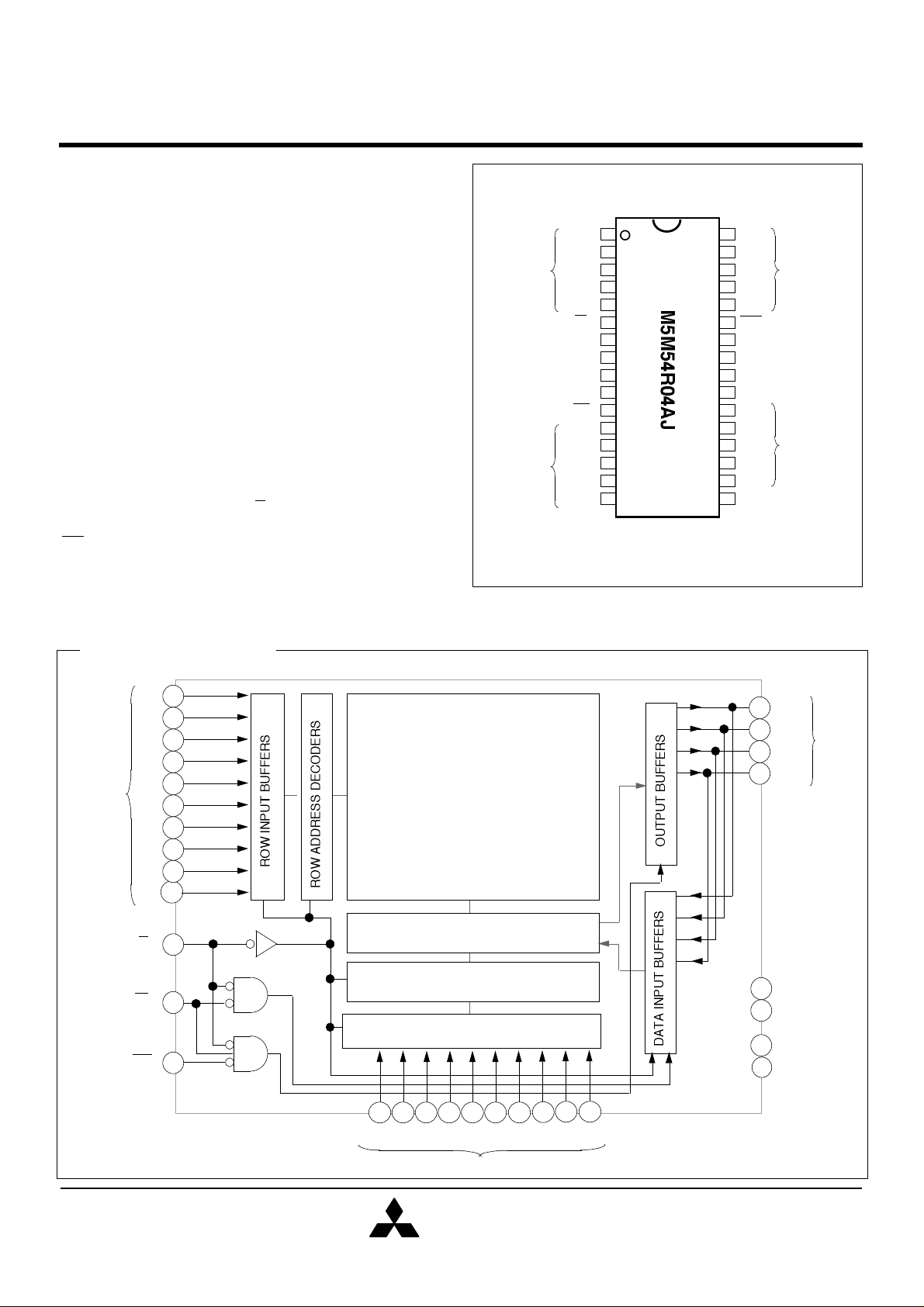
BLOCK DIAGRAM
address
Notice: This is not a final specification.
Some parametric limits are subject to change
MITSUBISHI LSIs
M5M54R04AJ-10,-12,-15
4194304-BIT (1048576-WORD BY 4-BIT) CMOS STATIC RAM
DESCRIPTION
FEATURES
•Fast access time M5M54R04AJ-10 ... 10ns(max)
M5M54R04AJ-12 ... 12ns(max)
M5M54R04AJ-15 ... 15ns(max)
•Single +3.3V power supply
•Fully static operation : No clocks, No refresh
•Common data I/O
•Easy memory expansion by S
•Three-state outputs : OR-tie capability
•OE prevents data contention in the I/O bus
•Directly TTL compatible : All inputs and outputs
APPLICATION
High-speed memory units
PIN CONFIGURATION (TOP VIEW)
A0
A1
(0V)
A2
A3
A4
S
DQ1
VCC
GND
DQ2
W
A5
inputs
chip select
input
datainputs/
outputs
(3.3V)
datainputs/
outputs
write control
input
A6
inputs
A7
A8
A9
Outline 32P0K(SOJ)
PACKAGE
M5M54R04AJ : 32pin 400mil SOJ
A19
A18
A17
A16
A15
output enable
OE
input
DQ4
(0V)
GND
(3.3V)
VCC
DQ3
A14
A13
A12
A11
A10
NC
inputs
datainputs/
outputs
datainputs/
outputs
inputs
A0
1
A1
2
A2
3
A3
adress
inputs
A4
A5
12
A6
13
A7
14
A8
15
A9
S 6
W
11
OE 27
4
5
COLUMN I/O CIRCUITS
COLUMN INPUT BUFFERS
18 19
MEMORY ARRAY
1024 ROWS
4096 COLUMNS
COLUMN ADDRESS
DECODERS
20 21 221628 29
inputs
MITSUBISHI
ELECTRIC
A16A15A14A13A12A11A10
31
A1730A18
32
A19
10
23
26
8
24
25
DQ1
7
DQ2
DQ3
DQ4
data
inputs/
outputs
VCC
(3.3V)
9
GND
(0V)
1
Output voltage
The operation mode of the M5M54R04AJ is determined by a
combination of the device control inputs S, W and OE. Each
mode is summarized in the function table.
A write cycle is executed whenever the low level W
overlaps with the low level S. The address must be set-up
before the write cycle and must be stable during the entire
cycle.
The data is latched into a cell on the trailing edge of W or
S, whichever occurs first, requiring the set-up and hold time
relative to these edge to be maintained. The output enable
input OE directly controls the output stage. Setting the OE at
a high level, the output stage is in a high impedance state,
and the data bus
A read cycle is excuted by setting W at a high level and
OE at a low level while S are in an active state (S=L).
When setting S at high level, the chip is in a nonselectable mode in which both reading and writing are
disable. In this mode, the output stage is in a highimpedance state, allowing OR-tie with other chips and
memory expansion by S.
Signal-S controls the power-down feature. When S goes
high, power dissapation is reduced extremely. The access
time from S is equivalent to the address access time.
FUNCTION
FUNCTION TABLE
S W OE
H
X X
L
L X
L Read
H L
L ActiveHigh-impedance
H H
Mode
Non selection Stand by
Write ActiveDin
High-impedance
MITSUBISHI LSIs
M5M54R04AJ-10,-12,-15
4194304-BIT (1048576-WORD BY 4-BIT) CMOS STATIC RAM
contention problem in the write cycle is eliminated.
DQ
Icc
ActiveDout
ABSOLUTE MAXIMUM RATINGS
Symbol
Vcc
VI
V
O
Pd
Topr
Tstg(bias)
T
stg
* Pulse width≤3ns, In case of DC: - 0.5V
Parameter
Supply voltage
Input voltage
Power dissipation
Operating temperature
Storage temperature(bias)
Storage temperature
With respect to GND
Ta=25°C
DC ELECTRICAL CHARACTERISTICS (Ta=0 ~ 70°C, Vcc=3.3V ,unless otherwise noted)
Symbol Parameter
V
IH
High-level input voltage
V
Low-level input voltage
IL
VOH
High-level output voltage
VOL 0.4
Low-level output voltage
Input current
I
I
I
Output current in off-state
OZ
Active supply current
I
CC1
(TTL level)
Stand by current
I
CC2
(TTL level)
I
Stand by current
CC3
Note 1: Direction for current flowing into an IC is positive (no mark).
I
= - 4mA
OH
IOL = 8mA
VI= 0 ~ Vcc
VI(S)=VIH
VI/O= 0 ~ Vcc
VI(S)=VIL
other inpus=VIH or VIL
Output-open(duty 100%)
VI(S)=VIH
VI(S)=Vcc≥0.2V
other inputs VI≤0.2V
or VI ≥Vcc - 0.2V
Condition
MITSUBISHI
ELECTRIC
Ratings
*
- 2.0 ~ 4.6
*
- 2.0 ~ VCC+0.5
*
- 2.0 ~ VCC
1000
0 ~ 70
- 10 ~ 85
- 65 ~ 150
+10%
- 5%
10ns cycle
12ns cycle
AC
15ns cycle
DC
10ns cycle
12ns cycle
AC
15ns cycle
DC 40
UnitConditions
Min
2.0
2.4
V
V
V
mW
°C
°C
°C
Limits
MaxTyp
Vcc+0.3
0.8
190
180
160
90
90
70
60
10
Unit
V
V
V
V
uA
2
2
uA
mA
mA
mA
2

MITSUBISHI LSIs
Input timing reference levels ........................ VIH=1.5V, VIL=1.5V
Output timing reference levels ................. VOH =1.5V, VOL=1.5V
Output loads ........................................................ Fig.1,Fig.2
M5M54R04AJ-10,-12,-15
4194304-BIT (1048576-WORD BY 4-BIT) CMOS STATIC RAM
CAPACITANCE (Ta=0~70°C, Vcc=3.3V ,unless otherwise noted)
Symbol Parameter
CI
Input capacitance
Output capacitance
CO
Note 2: CI,CO are periodically sampled and are not 100% tested.
AC ELECTRICAL CHARACTERISTICS (Ta=0~70°C, Vcc=3.3V ,unless otherwise noted)
+10%
-5%
Test Condition
VI=GND,VI=25mVrms,f=1MHz
VO=GND,
V
O=25mVrms,f=1MHz
Limit
MaxTypMin
7
8
+10%
-5%
(1)MEASUREMENT CONDITION
Input pulse levels .................................... VIH=3.0V, VIL=0.0V
Input rise and fall time .................................................... 3ns
5.0V
OUTPUT
Z0=50Ω
480Ω
Unit
pF
pF
RL=50Ω
VL=1.5V
Fig.1 Output load
DQ
DQ
255Ω
5pF
(including
scope and JIG)
Fig.2 Output load for t , ten dis
MITSUBISHI
ELECTRIC
3

(2)READ CYCLE
Write cycle time
Chip select access time
Symbol Parameter
tCR
ta(A)
ta(S)
ta(OE)
tdis(S)
tdis(OE)
ten(S)
ten(OE)
tv(A) Data valid time after address change
tPU Power-up time after chip selection
tPD
Read cycle time
Address access time
Output enable access time
Output disable time after S high
Output disable time after OE high 5 6 70 0
Output enable time after S low
Output enable time after OE low
Power-down time after chip selection
MITSUBISHI LSIs
M5M54R04AJ-10,-12,-15
4194304-BIT (1048576-WORD BY 4-BIT) CMOS STATIC RAM
Limits
M5M54R04AJ-10 M5M54R04AJ-12 M5M54R04AJ-15
Min
Max
Min MaxMin
10 12 15
10 12 15
10 12 15
5 6 70 0 0
2 3
0 1
2 3
0 0 0
10 12 15
Max
0
3
1
3
Unit
ns
ns
ns
ns5 6 7
ns
ns
ns
ns
ns
ns
ns
(3)WRITE CYCLE
Symbol
t
CW
tw(W)
tw(W)
tsu(A)1
Write pulse width (OE low)
Write pulse width(OE high)
Address setup time(W)
tsu(A)2 Address setup time(S)
tsu(S)
tsu(D)
th(D)
trec(W)
tdis(W)
tdis(OE)
ten(W)
ten(OE)
Chip select setup time
Data setup time
Data hold time
Write recovery time
Output disable time after W low
Output disable time after OE high
Output enable time after W high
Output enable time after OE low
tsu(A-WH) Address to W High
Parameter
Limits
M5M54R04AJ-10 M5M54R04AJ-12 M5M54R04AJ-15
MaxMin MaxMin MaxMin
10
12 15
10 12 15
8
0
0
8
10
0 0
0
10
10
0
10
5 6 7
0
1
0
0
5
5
0
0
8
0 0
1 1
0 0
0 0
6 7
6 7
0 0
0 0
10
10
Unit
ns
ns
ns
ns
ns
ns
ns
ns
ns
ns
ns
ns
ns
ns
MITSUBISHI
ELECTRIC
4
(4)TIMING DIAGRAMS
Read cycle 1
A
0~19
DQ1~4
VIH
VIL
VOH
VOL
W=H
S=L
OE=L
Read cycle 2 (Note 3)
VIH
S
VIL
M5M54R04AJ-10,-12,-15
4194304-BIT (1048576-WORD BY 4-BIT) CMOS STATIC RAM
t CR
ta(A)
tv(A)
PREVIOUS DATA VALID UNKNOWN DATA VALID
t
CR
ta(S)
(Note 4)
ten(S)
tv(A)
tdis(S)
MITSUBISHI LSIs
(Note 4)
DQ1~4
VOH
VOL
Icc
ICC1
ICC2
Note 3. Addresses valid prior to or coincident with S transition low.
4. Transition is measured ±500mv from steady state voltage with specified loading in Figure 2.
Read cycle 3 (Note 5)
VIH
OE
VIL
VOH
DQ1~4
VOL
W=H
OE=L
(Note 4)
UNKNOWN
DATA VALID
tPU
50% 50%
t
CR
ta(OE)
tdis(OE)
ten(OE)
UNKNOWN DATA VALID
tPD
(Note 4)
W=H
S=L
Note 5. Addresses and S valid prior to OE transition low by (ta(A)-ta(OE)), (ta(S)-ta(OE))
MITSUBISHI
ELECTRIC
5
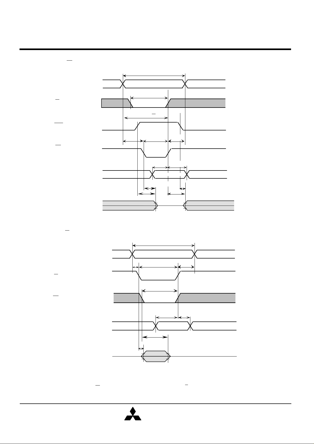
Write cycle (W control mode)
DATA STABLE
DATA STABLE
(Output Data)
A
S
OE
0~19
VIH
VIL
VIH
VIL
VIH
VIL
(Note 6)
tsu(A)
MITSUBISHI LSIs
M5M54R04AJ-10,-12,-15
4194304-BIT (1048576-WORD BY 4-BIT) CMOS STATIC RAM
tCW
tsu(S)
tsu(A-WH)
tw(W)
trec(W)
(Note 6)
W
DQ1~4
(Input Data)
DQ1~4
(Output Data)
VIH
VIL
VIH
VIL
VOH
VOL
Write cycle(S control)
A0~19
S
W
VIH
VIL
VIH
VIL
VIH
VIL
tdis(OE)
tsu(A)
(Note 6)
tsu(D)
tdis(W)
tsu(S)
tw(W)
(Note 4)
Hi-Z
tCW
tsu(D)
th(D)
th(D)
ten(OE)
ten(W)
trec(W)
(Note 4)
(Note 6)
DQ1~4
(Input Data)
VIH
VIL
tdis(W)
ten(S)
DQ1~4
Note 6: Hatching indicates the state is don't care.
7: When the falling edge of W is simultaneous or prior to the falling edge of S, the output is maintained in the high impedance.
8: ten,tdis are periodically sampled and are not 100% tested.
VOH
VOL
(Note 4)
(Note 4)
Hi-Z
(Note 7)
MITSUBISHI
ELECTRIC
6
 Loading...