

Mitsubishi M5M51R16AWG-10HI, M5M51R16AWG-15LI, M5M51R16AWG-15HI, M5M51R16AWG-12LI, M5M51R16AWG-12HI Datasheet
...
MITSUBISHI LSIs
FEATURE
NC : NO CONNECTION
M5M51R16AWG -10LI, -12LI, -15LI,
-10HI, -12HI, -15HI
1048576-BIT(65536-WORD BY 16-BIT)CMOS STATIC RAM
DESCRIPTION
The M5M51R16AWG is a 1048576-bit CMOS static RAM
organized as 65536 words by 16-bits, which are fabricated using
high-performance CMOS technology. The use of CMOS cells and
periphery results in a high density and low power static RAM.
The M5M51R16AWG can achieve low stand-by current and low
operation current and ideal for the battery back-up application.
The M5M51R16AWG is packaged in a 48-pin chip scale package
which is a high reliability and high density surface mount device
(SMD). Using this type of devices, it becomes very easy to design
a small system.
The M5M51R16AWG is fully compatible with the M5M51R16WG.
Power supply current
Type name
Access time
(max)
Active
(max)
Stand-by
(max)
M5M51R16AWG- 10LI 100ns
M5M51R16AWG- 12LI 120ns
M5M51R16AWG- 15LI 150ns
M5M51R16AWG- 10HI 100ns
M5M51R16AWG- 12HI 120ns
10mA
(1MHz)
4µA
2µA
M5M51R16AWG- 15HI 150ns
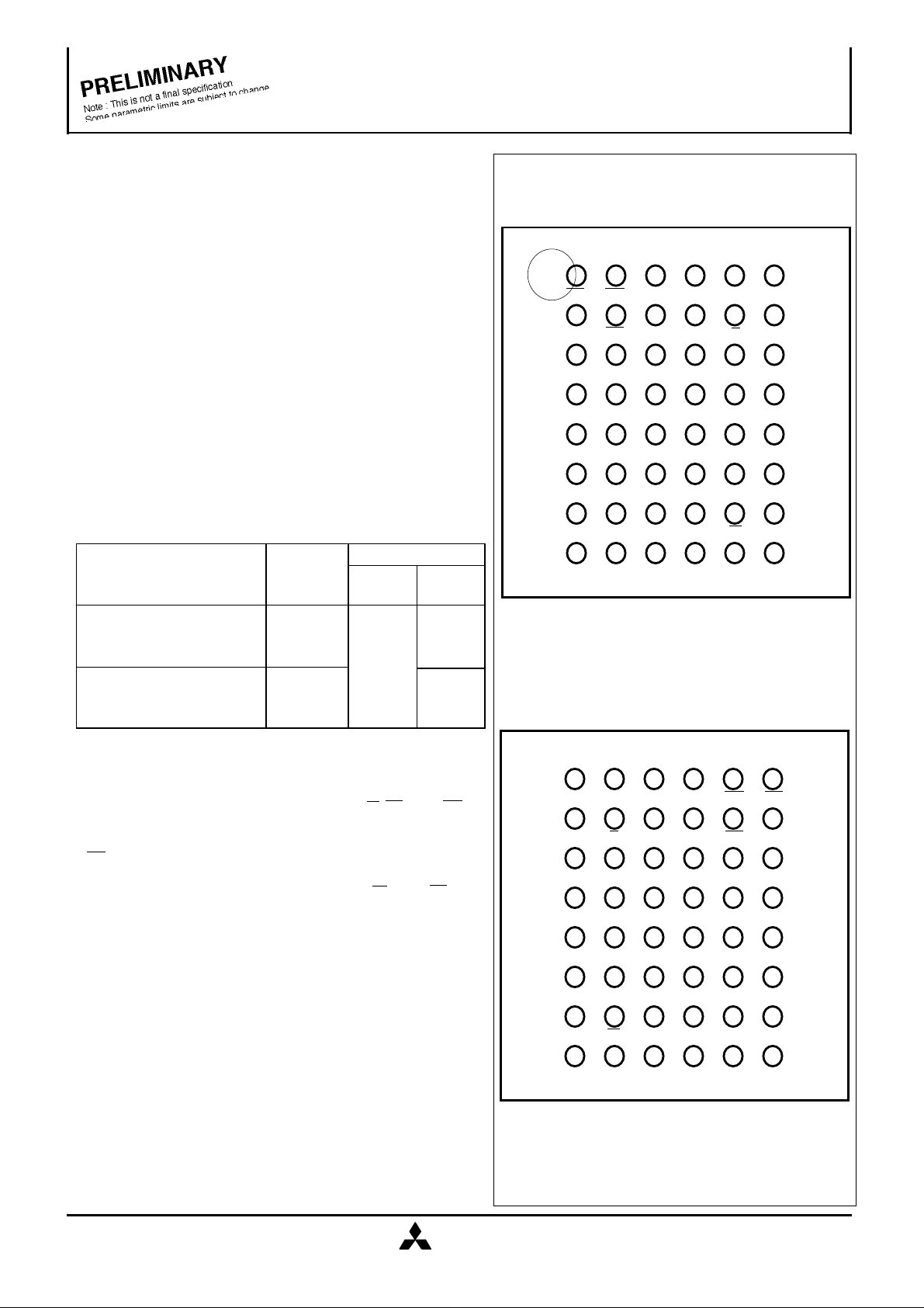
PIN CONFIGURATION (TOP VIEW)
1 2 3 4 5 6
A
A3
OEBC1
A6
A0
B
DQ16
BC2
A7
S
A2
C
A1
DQ15DQ14
A5
DQ2
D
DQ13
GND
NC
A4
DQ4
E
DQ12
NC
GNDVCC
DQ5
GND
F
DQ11 DQ10
A9
A14
DQ7
G
DQ9
NC
A10
A13
W
H
A8
NC NC
A11
A12
A15
PIN CONFIGURATION (BOTTOM VIEW)
NC
DQ1
DQ3
VCC
DQ6
DQ8
• Single +1.8V~2.7V power supply
• Low power down current 0.05µA(typ.)
• Directly TTL compatible : All inputs and outputs
• Easy memory expansion and power down by S,BC1 and BC2
• Data hold on +1.0V power supply
• Three-state outputs : OR-tie capability
• OE prevents data contention in the I/O bus
• Common data I/O
• Separate control of lower and upper bytes by BC1 and BC2
• Package
48-pin chip scale package(CSP)
Ball pitch : 0.75mm
Package size: 7.0mm x 8.5mm
APPLICATION
Small capacity memory units.
6 5 4 3 2 1
A
A3
A0
NC
B
DQ1
A2
S
C
DQ3
DQ2
A1
D
DQ4
VCC
A4
E
NC
DQ5
GND
F
DQ6
DQ7
A14
G
DQ8
H
W
A15
A13
A12
Outline 48FJA
A6
A7
A5
NC
GND
A9
A10
A11
OE
BC1
BC2
DQ16
DQ15 DQ14
DQ13
GND
DQ12
VCC
DQ11DQ10
DQ9
NC
A8
NCNC
Aug.1. 1998
MITSUBISHI
ELECTRIC
1
FUNCTION
(High-Z=High-impedance)
Mode
DQ1~8
DQ9~16
Icc
Non selection
LXXXX
High-Z
XHHXX
High-Z
Stand-by
Upper-Byte Write
HHLLX
Din
Active
Upper-Byte Read
LLHigh-Z
Dout
Active
HLH
High-Z
Active
Lower-Byte Write
LHLXHigh-Z
Din
Active
Lower-Byte Read
LHX
High-Z
Dout
Active
LHH
High-Z
High-Z
Stand-by
Word Write
HLLLX
Din
Word Read
LLL
Dout
Active
HLL
High-Z
High-Z
Active
Din
DoutWOESBC1
BC2LLLX
Output disable
Non selection
(Lower-Byte Non selection)
(Lower-Byte Non selection)
(Upper-Byte Non selection)
(Upper-Byte Non selection)
65536 WORDS x16 BITS
ADDRESS
CHIP SELECT
INPUT
BC2
BC1
BYTE
CONTROL
INPUTS
WRITE CONTROL
INPUT
OUTPUT ENABLE
INPUT
DATA
INPUTS/
OUTPUTS
INPUTS
A4D4A3A4A2B4A1C4A0A5A15H5A14F4A13G4A12H4A8H2A9F3A10G3A11H3A7B3A5C3A6A3B5G5A2B2WOESA1B6
DQ1C5DQ2C6DQ3D5DQ4E5DQ5F6DQ6F5DQ7G6DQ8G1DQ9F2DQ10F1DQ11E2DQ12D2DQ13C1DQ14C2DQ15B1DQ16E1VccE6GND
(0V)D1GND
(0V)
Vcc
D6E3GND
(0V)
The operation mode of the M5M51R16A series are
determined by a combination of the device control
inputs S, W, OE, BC1 and BC2. Each mode is
summarized in the function table.
A write cycle is executed whenever the low level W
overlaps with the low level BC1 and/or BC2 and the
low level S. The address must be set up before the
write cycle and must be stable during the entire cycle.
The data is latched into a cell on the trailing edge of
W, BC1, BC2 or S, whichever occurs first, requiring
the set-up and hold time relative to these edge to be
maintained. The output enable input OE directly
controls the output stage. Setting the OE at a high
level, the output stage is in a high-impedance state,
and the data bus contention problem in the write cycle
is eliminated.
A read cycle is executed by setting W at a high level
and OE at a low level while BC1 and/or BC2 and S
are in an active state. (BC1 and/or BC2=L, S=L)
When setting BC1 at a high level and the other pins
are in an active state, upper-Byte are in a selectable
mode in which both reading and writing are enabled,
and lower -Byte are in a non-selectable mode. And
when setting BC2 at a high level and the other pins
are in an active state, lower-Byte are in a selectable
mode in which both reading and writing are enabled,
and upper -Byte are in a non-selectable mode.
MITSUBISHI LSIs
M5M51R16AWG -10LI, -12LI, -15LI,
-10HI, -12HI, -15HI
1048576-BIT(65536-WORD BY 16-BIT)CMOS STATIC RAM
When setting BC1 and BC2 at a high level or S at
a high level, the chips are in a non-selectable mode in
which both reading and writing are disabled.
In this mode, the output stage is in a high-impedance
state, allowing OR -tie with other chips and memory
expansion by BC1, BC2 and S. S, BC1 and BC2
control the power down feature. When S, BC1 and
BC2 go high, the power supply current is reduced as
low as the stand-by current which is specified as Icc3
or Icc4, and the memory data can be held at +1.0V
power supply, enabling battery back-up operation
during power-failure or power-down operation in the
non-selected mode.
FUNCTION TABLE
BLOCK DIAGRAM
( 512 ROWS
x 256 COLUMNS
x 8 BLOCKS )
CLOCK
GENERATOR
Aug.1. 1998
MITSUBISHI
ELECTRIC
2
M5M51R16AWG -10LI, -12LI, -15LI,
and
-10HI, -12HI, -15HI
1048576-BIT(65536-WORD BY 16-BIT)CMOS STATIC RAM
ABSOLUTE MAXIMUM RATINGS
Symbol
Vcc
VI
Vo
Pd
Topr
Tstg
* -1.0V in case of AC ( Pulse width ≤ 30ns )
DC ELECTRICAL CHARACTERISTICS ( Ta = - 40~85°C, Vcc = 1.8V~2.7V, unless otherwise noted )
Symbol Parameter
VIH
VIL
VOH
VOL
II
Io
ICC1W
ICC2W
ICC1B
ICC2B
ICC3
ICC4
Output current in off-state
Word operation(16bit)
Active supply current
Byte operation(8bit)
Active supply current
Stand-by current
Parameter
Supply voltage
Input voltage
Output voltage
Power dissipation
Operating temperature
Storage temperature
High-level input voltage
Low-level input voltage
High-level output voltage
Low-level output voltage
Input current
(AC,TTL level)
(AC,TTL level)
Stand-by current
Conditions
With respect to GND
Ta=25°C
IOH = -0.1mA
IOL = 0.1mA
VI =0 ~Vcc
BC1 and BC2 = VIH or S = VIH or
OE = VIH, VI/O = 0~ Vcc
BC1 and BC2 = VIL, S = VIL
other inputs = VIH or VIL
Output-open(duty 100%)
(BC1 = VIH and BC2 = VIL) or (BC1 = VIL
BC2 = VIH) , S = VIL ,other inputs = VIH or VIL
Output-open(duty 100%)
1) S≥Vcc-0.2V, other inputs = 0~Vcc
2) BC1 and BC2 ≥Vcc-0.2V,S≤0.2V,
other inputs = 0~Vcc
BC1 and BC2 = VIH or S = VIH,
other inputs = 0~Vcc
-0.2* ~ Vcc+0.2(max.4.6V)
Conditions
Ratings
-0.2 ~ 4.6
0 ~ Vcc
1
-40 ~ 85
-65 ~150
Min
cycle
1MHz
Min
cycle
1MHz
-LI
-HI
Unit
V
V
V
W
°C
°C
Min
0.7 x Vcc
-0.2*
1.6
MITSUBISHI LSIs
Limits
Typ
Max
Vcc+0.2V
0.4
0.2
±1
±1
15
7
10
25
10
5
8
4
2
0.3
Unit
V
V
V
V
µA
µA
mA
mA
mA15
mA
µA
µA
mA
* -1.0V in case of AC ( Pulse width ≤ 30ns )
CAPACITANCE ( Ta = - 40 ~85°C, Vcc = 1.8V~2.7V, unless otherwise noted )
Symbol Parameter Conditions
Input capacitance
CI
Output capacitance
CO
Note 1: Direction for current flowing into an IC is positive (no mark).
Note 2: Typical value is Vcc = 2.0V, Ta = 25°C
Note 3: CI,CO are periodically sampled and are not 100% tested.
Aug.1. 1998
VI=GND, Vi=25mVrms, f=1MHz
VO=GND, Vo=25mVrms, f=1MHz
MITSUBISHI
ELECTRIC
Min
Typ
Limits
Max
6
10
Unit
pF
pF
3
 Loading...