

Mitsubishi M37272MA-XXXSP, M37272M8-XXXSP, M37272M8-XXXFP, M37272M6-XXXSP, M37272M6-XXXFP Datasheet
...
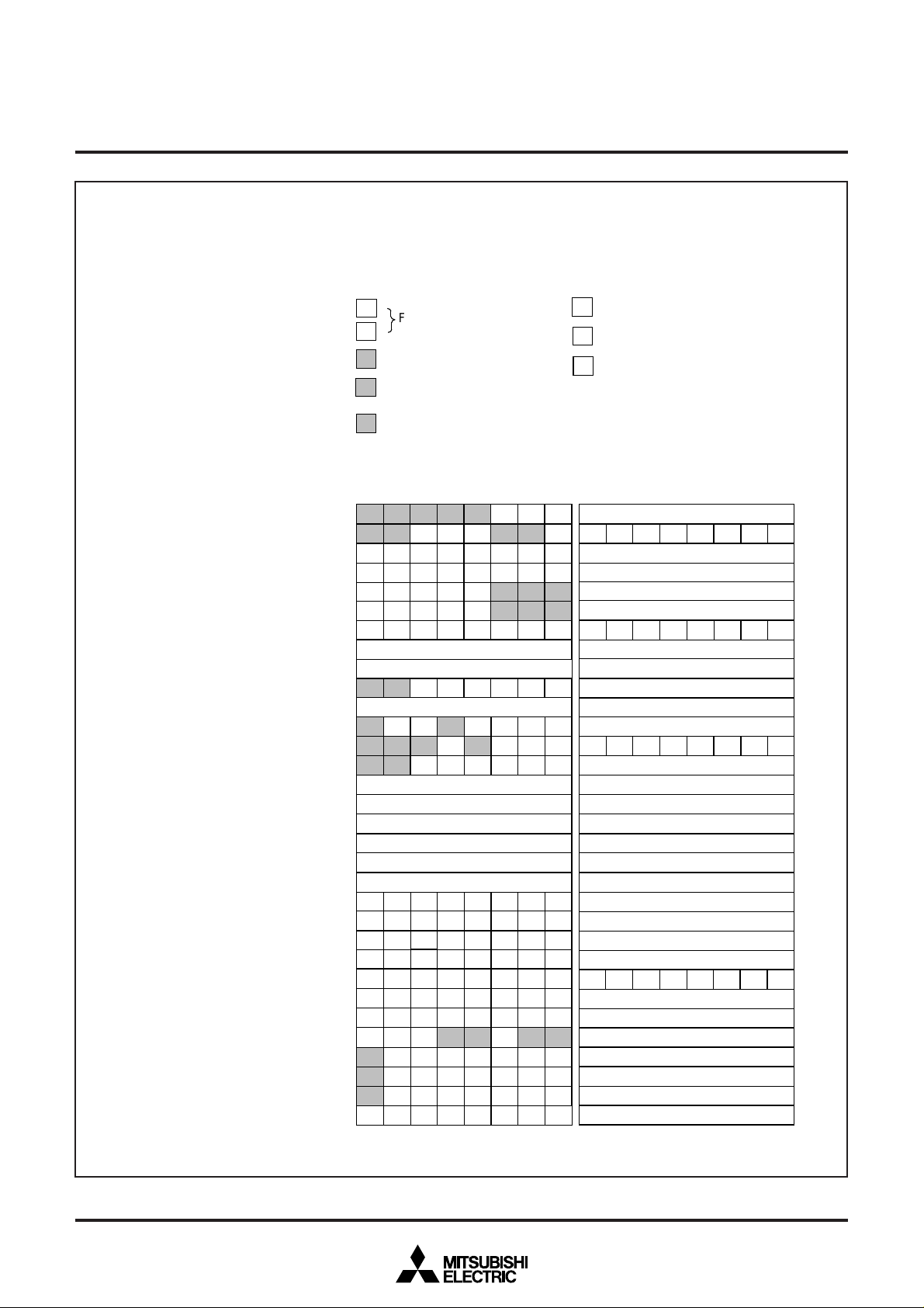
MITSUBISHI MICROCOMPUTERS
M37272M6/M8–XXXSP/FP, M37272MA–XXXSP
M37272E8SP/FP, M37272EFSP
SINGLE-CHIP 8-BIT CMOS MICROCOMPUTER with CLOSED CAPTION DECODER
and ON-SCREEN DISPLAY CONTROLLER
1. DESCRIPTION
The M37272M6/M8-XXXSP/FP and M37272MA-XXXSP are singlechip microcomputers designed with CMOS silicon gate technology.
They have a OSD, data slicer, and I
for a channel selection system for TV with a closed caption decoder .
The features of the M37272E8SP/FP and M37272EFSP are similar
to those of the M37272M6-XXXSP except that the chip has a built-in
PROM which can be written electrically. The difference between
M37272M6-XXXSP/FP, M37272M8-XXXSP/FP and M37272MAXXXSP are the ROM size and RAM size. Accordingly, the following
descriptions will be for the M37272M6-XXXSP/FP.
2
C-BUS interface, so it is useful
2. FEATURES
●Number of basic instructions .................................................... 71
●Memory size
ROM .............. 24K bytes
(
M37272M6-XXXSP/FP
32K bytes
(
M37272M8-XXXSP/FP, M37272E8SP/FP
40K bytes
(
M37272MA-XXXSP
60K bytes
(
M37272EFSP
RAM ...............
(*ROM correction memory included)
●Minimum instruction execution time
......................................... 0.5 µs
●Power source voltage ................................................. 5 V ± 10 %
●Subroutine nesting .............................................128 levels (Max.)
●Interrupts....................................................... 17 types, 16 vectors
●8-bit timers .................................................................................. 6
●Programmable I/O ports (Ports P0, P1, P2, P3
●Input ports (Ports P5
●Output ports (Ports P5
●12 V withstand ports ................................................................... 6
●LED drive ports ........................................................................... 4
●Serial I/O ............................................................8-bit ✕ 1 channel
●Multi-master I
●A-D comparator (6-bit resolution) ................................6 channels
●PWM output circuit......................................................... 8-bit ✕ 6
●Power dissipation
In high-speed mode .........................................................165 mW
(at V
CC = 5.5V, 8 MHz oscillation frequency, OSD on, and Data
slicer on)
In low-speed mode .........................................................0.33 mW
(at V
CC = 5.5V, 32 kHz oscillation frequency)
●ROM correction function ................................................ 2 vectors
●Closed caption data slicer
2
C-BUS interface .............................. 1 (2 systems)
1024
bytes
(
M37272M6-XXXSP/FP
1152
bytes
M37272M8-XXXSP/FP, M37272E8SP/FP
(
1472
bytes
(
M37272MA-XXXSP, M37272EFSP
(at 8 MHz oscillation frequency)
0, P51) ........................................................ 2
2–P55) ..................................................... 4
)
)
)
)
)
0, P31) ............. 26
●OSD function
Display characters ................................... 32 characters ✕ 2 lines
Kinds of characters ........................................................254 kinds
Character display area............................ CC mode: 16 ✕ 26 dots
Kinds of character sizes..................................... CC mode: 1 kind
Kinds of character colors .................................. 8 colors (R, G, B)
Coloring unit................... character, character background, raster
Display position
Horizontal: 128 levels Vertical: 512 levels
Attribute ........................................................................................
CC mode: smooth italic, underline, flash, automatic solid space
OSD mode: border
Smoth roll-up
Window function
3. APPLICA TION
)
TV with a closed caption decoder
)
(It is possible to display 3 lines or more by software)
OSD mode: 16 ✕ 20 dots
OSD mode: 8 kinds
Rev. 1.5

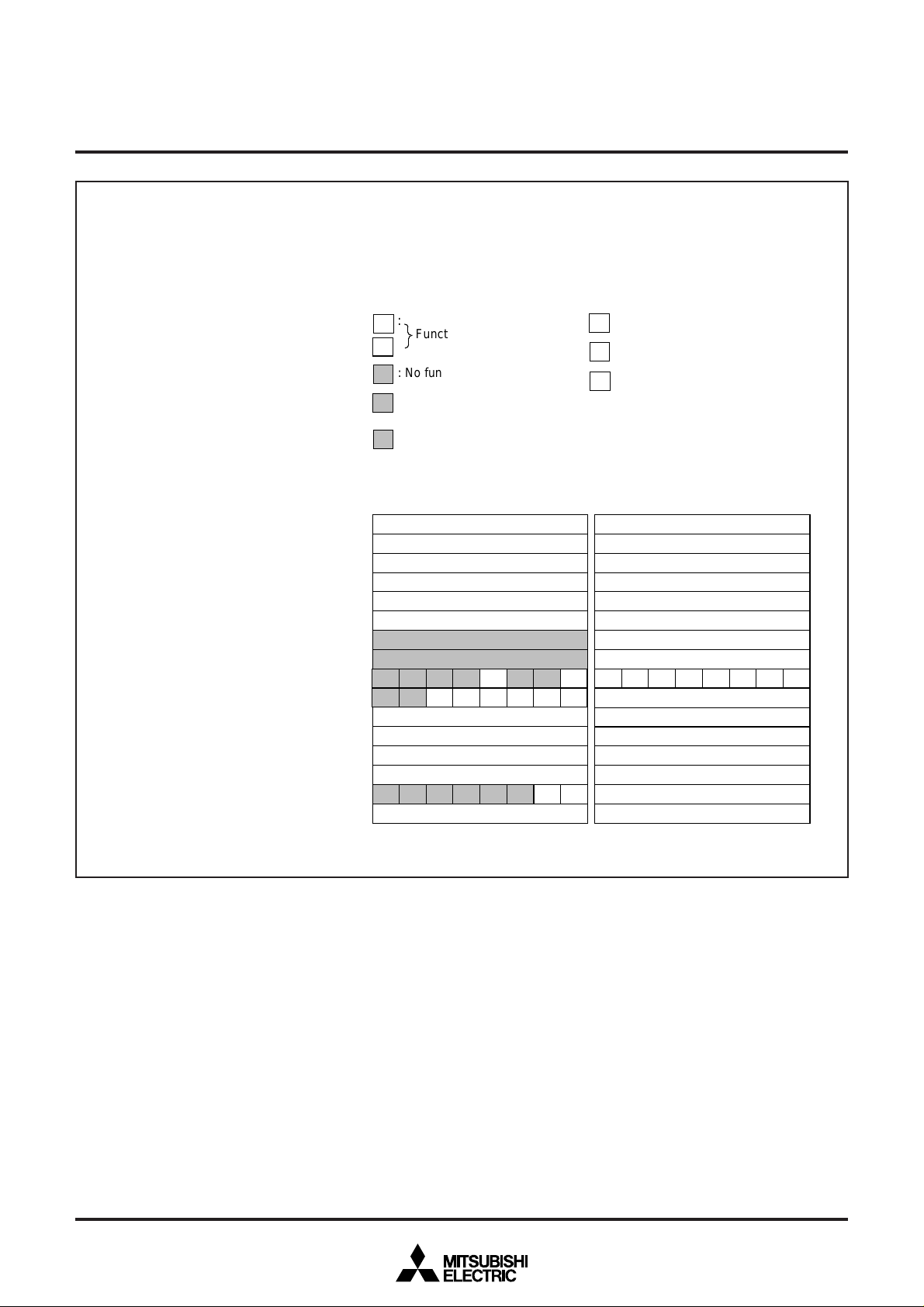
TABLE OF CONTENTS
MITSUBISHI MICROCOMPUTERS
M37272M6/M8–XXXSP/FP, M37272MA–XXXSP
M37272E8SP/FP, M37272EFSP
SINGLE-CHIP 8-BIT CMOS MICROCOMPUTER with CLOSED CAPTION DECODER
and ON-SCREEN DISPLAY CONTROLLER
1. DESCRIPTION ..........................................................................1
2. FEAUTURES .............................................................................1
3. APPLICATION............................................................................1
4. PIN CONFIGURATION ..............................................................3
5. FUNCTIONAL BLOCK DIAGRAM .............................................4
6. PERFORMANCE OVERVIEW...................................................5
7. PIN DESCRIPTION ...................................................................7
8. FUNCTIONAL DESCRIPTION................................................. 11
8.1 CENTRAL PROCESSING UNIT (CPU) ....................11
8.2 MEMORY ..................................................................12
8.3 INTERRUPTS ...........................................................18
8.4 TIMERS.....................................................................23
8.5 SERIAL I/O................................................................26
8.6 MULTI-MASTER I
8.7 PWM OUTPUT CIRCUIT ..........................................42
8.8 A-D COMPARA TOR ..................................................46
8.9 ROM CORRECTION FUNCTION .............................48
8.10 DATA SLICER .........................................................49
8.11 OSD FUNCTIONS...................................................60
8.11.1 Display Position .......................................65
8.11.2 Dot size....................................................69
8.11.3 Clock for OSD..........................................70
8.11.4 Field Determination Display.....................71
8.11.5 Memory For OSD..................................... 73
8.11.6 Character Color .......................................77
8.11.7 Character Background Color ...................77
8.11.8 OUT1, OUT2 Signals...............................78
8.11.9 Attribute....................................................79
8.11.10 Multiple Display......................................84
8.11.11 Automatic Solid Space Function ............85
8.11.12 Window Function ...................................86
8.11.13 OSD Output Pin Control ........................88
8.11.14 Raster Coloring Function.......................89
8.12. SOFTWARE RUNAWAY DETECT FUNCTION .....91
8.13. RESET CIRCUIT....................................................92
8.14. CLOCK GENERATING CIRCUIT...........................93
8.15. DISPLAY OSCILLATION CIRCUIT ........................96
8.16. AUTO-CLEAR CIRCUIT .........................................96
8.17. ADDRESSING MODE ............................................96
8.18. MACHINE INSTRUCTIONS...................................96
2
C-BUS INTERFACE....................29
9. PROGRAMMING NOTES........................................................96
10. ABSOLUTE MAXIMUM RATINGS .........................................97
11. RECOMMENDED OPERATING CONDITIONS.....................97
12. ELECTRIC CHARACTERISTICS ..........................................98
13. A-D COMPARISON CHARACTERISTICS...........................100
14.
MULTI-MASTER I2C-BUS BUS LINE CHARACTERISTICS .........
15. PROM PROGRAMMING METHOD..................................... 101
16. DATA REQUIRED FOR MASK ORDERS............................102
17. MASK CONFIRMATION FORM...........................................103
18. MARK SPECIFICATION FORM........................................... 112
19. ONE TIME PROM VERSIONS M37272E8SP/FP,
M37272EFSP MARKING..................................................... 114
20. APPENDIX ........................................................................... 1 15
21. PACKAGE OUTLINE ...........................................................140
100
Rev. 1.3
2
F
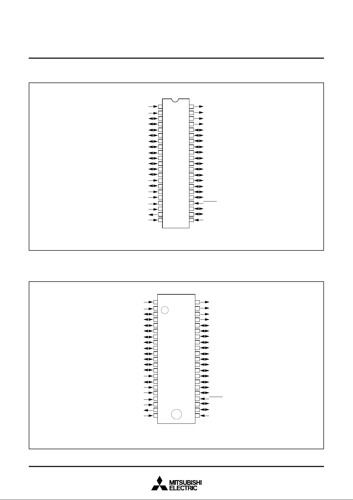
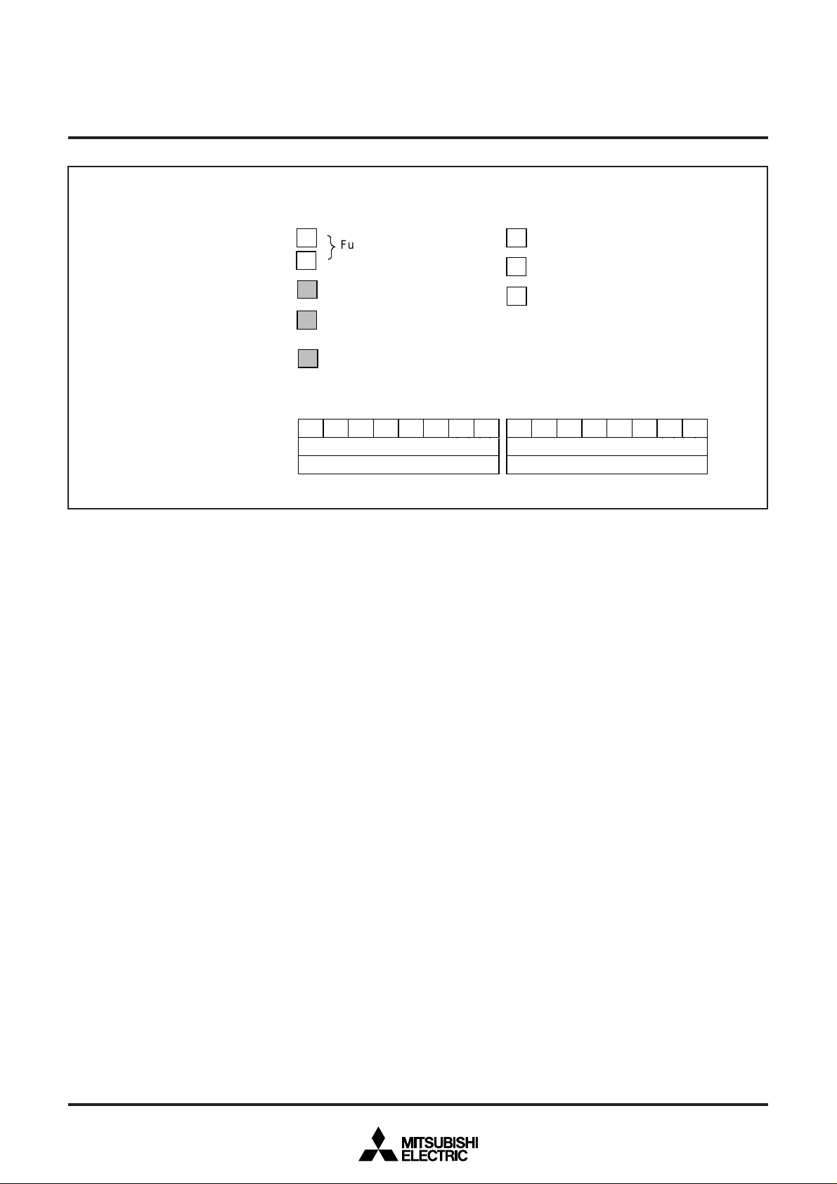
4. PIN CONFIGURATION
C
C
F
MITSUBISHI MICROCOMPUTERS
M37272M6/M8–XXXSP/FP, M37272MA–XXXSP
M37272E8SP/FP, M37272EFSP
SINGLE-CHIP 8-BIT CMOS MICROCOMPUTER with CLOSED CAPTION DECODER
and ON-SCREEN DISPLAY CONTROLLER
Fig. 4.1 Pin Configuration (1) (Top View)
P 50/ H
S Y N C
P 51/ V
S Y N C
P 00/ P W M 0
P 0
1
/ P W M 1
P 02/ P W M 2
P 03/ P W M 3
P 0
4
/ P W M 4
P 05/ P W M 5
P 06/ I N T 2 / A D 4
P 0
7
/ I N T 1
P 2
3
/ T I M 3
P 24/ T I M 2
P 2
A V
H L
V
H O L D
C V
C N V
X
X
O U T
V
1
2
3
4
5
6
7
8
9
1 0
1 1
1 2
5
1 3
1 4
C C
1 5
1 6
1 7
I N
1 8
S S
1 9
I N
2 0
2 1
S S
Outline 42P4B
4 2
P 52/ R
4 1
4 0
3 9
3 8
M
3 7 2 7 2 M 6 / M 8 / M A - X X X S PM
3 7 2 7 2 E 8 / E F S
3 7
3 6
3 5
3 4
3 3
3 2
P
3 1
3 0
2 9
2 8
2 7
2 6
2 5
2 4
2 3
2 2
3
/ G
P 5
P 5
4
/ B
P 55/ O U T 1
P 2
0
/ S
C L K
P 21/ S
O U T
P 22/ S
I N
P 10/ O U T 2
P 1
1
/ S C L 1
2
/ S C L 2
P 1
P 1
3
/ S D A 1
P 14/ S D A 2
P 1
5
/ A D 1 / I N T 3
P 16/ A D 2
P 17/ A D 3
P 3
0
/ A D 5
1
/ A D 6
P 3
R E S E T
P 2
6
/ O S C 1 / X
P 27/ O S C 2 / X
V
C C
C I N
C O U T
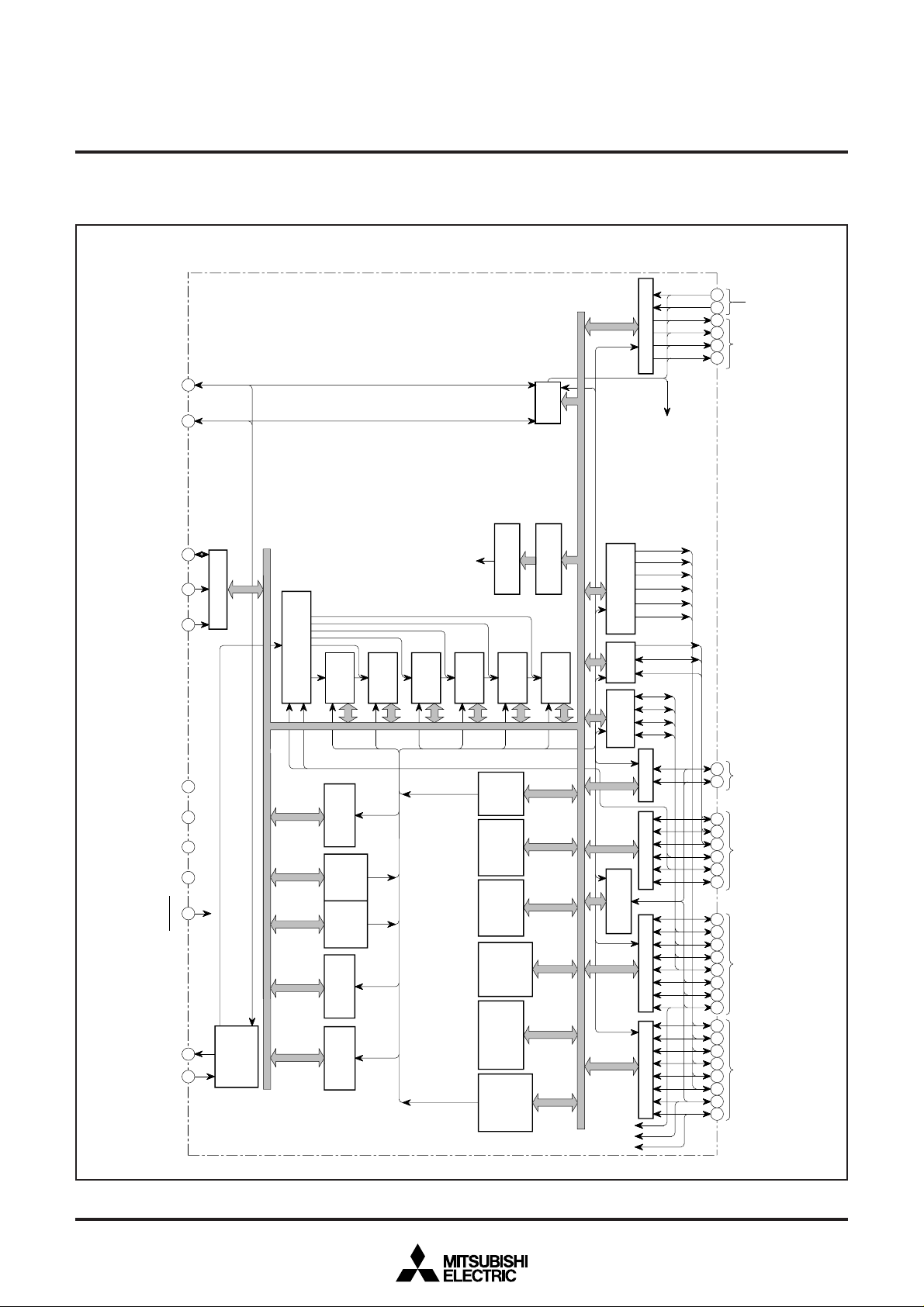
Fig. 4.2 Pin Configuration (2) (Top View)
Rev. 1.4
P 50/ H
S Y N
P 51/ V
S Y N
P 00/ P W M 0
1
/ P W M 1
P 0
2
/ P W M 2
P 0
3
/ P W M 3
P 0
4
/ P W M 4
P 0
5
/ P W M 5
P 0
P 06/ I N T 2 / A D 4
7
/ I N T 1
P 0
3
/ T I M 3
P 2
4
/ T I M 2
P 2
P 2
A V
H L
V
H O L D
C V
C N V
X
O U T
X
V
1
2
3
4
5
6
7
8
9
1 0
1 1
1 2
1 3
5
1 4
C C
1 5
1 6
1 7
I N
1 8
S S
1 9
I N
2 0
2 1
S S
M
P
Outline 42P2R-A/E
4 2
P 52/ R
4 1
4 0
3 9
3 8
3 7
3 7 2 7 2 M 6 / M 8 - X X X F PM
3 7 2 7 2 E 8 F
3 6
3 5
3 4
3 3
3 2
3 1
3 0
2 9
2 8
2 7
2 6
2 5
2 4
2 3
2 2
3
/ G
P 5
4
/ B
P 5
5
/ O U T 1
P 5
0
/ S
C L K
P 2
P 21/ S
O U T
P 22/ S
I N
P 10/ O U T 2
1
/ S C L 1
P 1
2
/ S C L 2
P 1
3
/ S D A 1
P 1
4
/ S D A 2
P 1
5
/ A D 1 / I N T 3
P 1
6
/ A D 2
P 1
P 17/ A D 3
0
/ A D 5
P 3
1
/ A D 6
P 3
R E S E T
6
/ O S C 1 / X
P 2
P 27/ O S C 2 / X
V
C C
C I N
C O U T
3
M37272M6/M8–XXXSP/FP, M37272MA–XXXSP
XI
N
XO
U
T
O
S C 1 /
XC
I
N
O
S C 2 /
X
C
O U
T
P
0 ( 8
)
I N T 1
I N T 2
I N T 3
P
1 ( 8
)
P W M 5
P W M 4
P W M 3
P W M 2
P W M 1
P W M 0
P
W
M
T
I M 2T
I M
3
1
92
02
51
42
22
11
8
C
VI
N
1
71
61
5
VH
O L
D
H
L
F
2
42
31
09
8765432
82
93
03
13
23
33
43
5
P
2 ( 8
)
1
31
21
1
3
6
3
7
I
/
O
p
o
r
t
P
1
I
/
O
p
o
r
t
P
2
P
3 ( 2
)
2
7
2
6
3
8
S D A 2
S D A 1
S C L 2
S C L 1
S
I
/
O
SI
N
SC
L
K
SO
U
T
P
5 ( 6
)
3
94
04
14
22
O
u
t
p
u
t
p
o
r
t
s
P
5
2–
P
55
O
u
t
p
u
t
f
o
r
d
i
s
p
l
a
y
1
H
S Y N C
V
S Y N C
R
G
B
O U T 1
O
U
T
2
P
10
I
/
O
p
o
r
t
s
P
3
0,
P
31
A D 1 – 6
D
a t a s l i c e rC
o n t r o l s i g n a
l
C
l
o
c
k
i
n
p
u
t
C
l o c k o u t p u tXI
N
XO
U
T
R
e s e t i n p u
t
A
VC
C
VC
C
VS
S
C
N
VS
S
P
i n s f o r d a t a s l i c e rC
l o c k o u t p u t f o r O S D /s
u b - c l o c k o u t p u tI
/ O p o r t s P
2
6,
P
27
C
l
o
c
k
i
n
p
u
t
f
o
r
O
S
D
/
s
u
b
-
c
l
o
c
k
i
n
p
u
t
A
-
D
c
o
m
p
a
r
a
t
o
r
8
- b i
t
a
r i t h m e t i
c
a
n d
l
o g i c a l u n i
t
A
c
c
u
m
u
l
a
t
o
r
A
(
8
)
T
i
m
e
r
6
T
6 ( 8
)
T
i
m
e
r
5
T
5 ( 8
)
T
i
m
e
r
4
T
4
(
8
)
T
i
m
e
r
3
T
3
(
8
)
T
i
m
e
r
2
T
2 ( 8
)
T
i
m
e
r
1
T
1 ( 8
)
T
i m e r c o u n t s o u r c
e
s
e l e c t i o n c i r c u i
t
I
n s t r u c t i o
n
r
e g i s t e r ( 8
)
I
n
s
t
r
u
c
t
i
o
n
d
e
c
o
d
e
r
O
S
D
c
i
r
c
u
i
t
P
r o c e s s o
r
s
t a t u
s
r
e g i s t e
r
P
S ( 8
)
S
t a c
k
p
o i n t e
r
S
( 8
)
I
n
d
e
x
r
e
g
i
s
t
e
r
Y
(
8
)
I
n
d
e
x
r
e
g
i
s
t
e
r
X
(
8
)
R
O
M
P
r o g r a
m
c
o u n t e
r
P
CL
(
8
)
P
r
o
g
a
m
c
o
u
n
t
e
r
P
CH
(
8
)
R
A
M
D
a t a b u
s
C
l
o
c
k
g
e
n
e
r
a
t
i
n
g
c
i
r
c
u
i
t
R
E S E TC
VI
N
A
d
d
r
e
s
s
b
u
s
I
/
O
p
o
r
t
P
0
R
O M c o r r e c t i o
n
c
i r c u i
t
M
u l t i - m a s t e r
I
2
C
- B U
S
i
n t e r f a c
e
I
n
p
u
t
p
o
r
t
s
P
5
0,
P
51
S
y
n
c
h
r
o
n
o
u
s
s
i
g
n
a
l
i
n
p
u
t
SINGLE-CHIP 8-BIT CMOS MICROCOMPUTER with CLOSED CAPTION DECODER
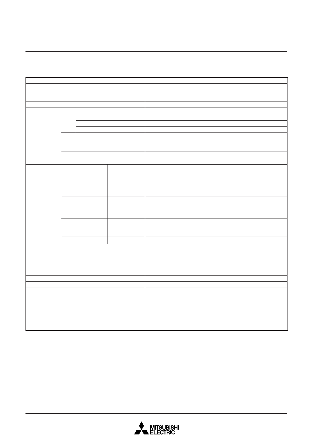
5. FUNCTIONAL BLOCK DIAGRAM
MITSUBISHI MICROCOMPUTERS
M37272E8SP/FP, M37272EFSP
and ON-SCREEN DISPLAY CONTROLLER
Fig. 5.1 Functional Block Diagram of M37272
4
Rev. 1.3
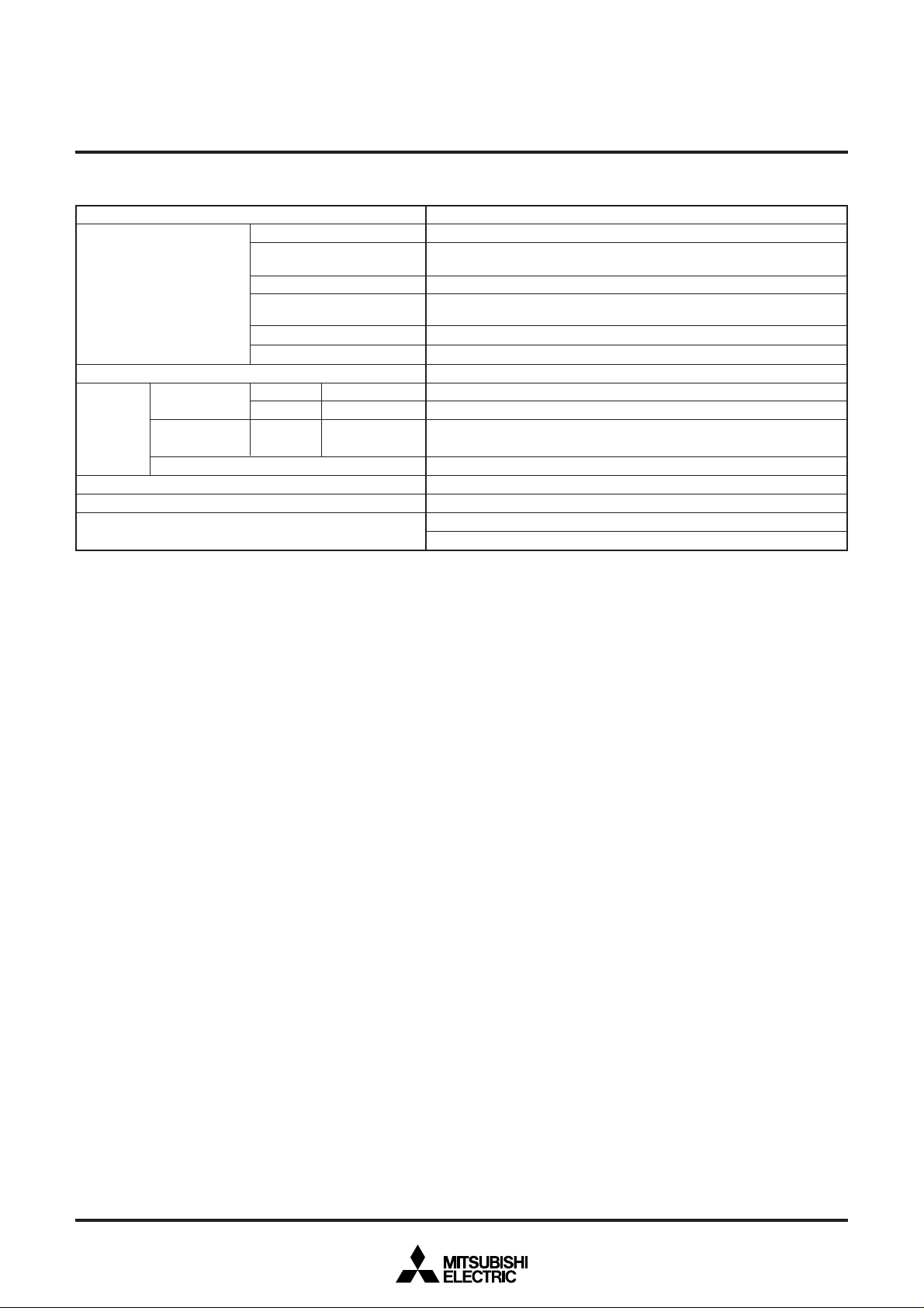
6. PERFORMANCE OVERVIEW
Table 6.1 Performance Overview
Parameter
Number of basic instructions
Instruction execution time
Clock frequency
Memory size
Input/Output
ports
Serial I/O
Multi-master I
A-D comparator
PWM output circuit
Timers
ROM correction function
Subroutine nesting
Interrupt
Clock generating circuit
Data slicer
ROM
M37272M6-XXXSP/FP
M37272M8-XXXSP/FP,M37272E8SP/FP
M37272MA-XXXSP
M37272EFSP
RAM
M37272M6-XXXSP/FP
M37272M8-XXXSP/FP,M37272E8SP/FP
M37272MA-XXXSP, M37272EFSP
OSD ROM
OSD RAM
P0
P1
0–P17
P20–P27
P30, P31
P50, P51
P52–P55
2
C-BUS interface
MITSUBISHI MICROCOMPUTERS
M37272M6/M8–XXXSP/FP, M37272MA–XXXSP
M37272E8SP/FP, M37272EFSP
SINGLE-CHIP 8-BIT CMOS MICROCOMPUTER with CLOSED CAPTION DECODER
and ON-SCREEN DISPLAY CONTROLLER
Functions
71
0.5 µs (the minimum instruction execution time, at 8 MHz oscillation frequency)
8 MHz (maximum)
24K bytes
32K bytes
40K bytes
60K bytes
1024 bytes (ROM correction memory included)
1152 bytes (ROM correction memory included)
1472 bytes (ROM correction memory included)
10K bytes
128 bytes
I/O
I/O
I/O
I/O
Input
Output
8-bit ✕ 1 (N-channel open-drain output structure, can be used as PWM
output pins, INT input pins, A-D input pin)
8-bit ✕ 1 (CMOS input/output structure, however, N-channel open-drain
output structure, when P1
face, can be used as OSD output pin, A-D input pins, INT input pin, multi-
2
master I
8-bit ✕ 1 (P2 is CMOS input/output structure, however, N-channel open-
drain output structure when P2
used as serial input/output pins, timer external clock input pins, OSD clock
input/output pin, sub-clock input/output pins)
2-bit ✕ 1 (CMOS input/output or N-channel open-drain output structure,
can be used as A-D input pins)
2-bit ✕ 1 (can be used as OSD input pins)
4-bit ✕ 1 (CMOS output structure, can be used as OSD output pins)
8-bit ✕ 1
1 (2 systems)
6 channels (6-bit resolution)
8-bit ✕ 6
8-bit timer ✕ 6
2 vectors
128 levels (maximum)
<17 types>
INT external interrupt ✕ 3, Internal timer interrupt ✕ 6, Serial I/O interrupt ✕
1, OSD interrupt ✕ 1, Multi-master I
slicer interrupt ✕ 1, f(X
instruction interrupt ✕ 1, reset ✕ 1
2 built-in circuits (externally connected to a ceramic resonator or a quartzcrystal oscillator)
Built-in
C-BUS interface)
1–P14 are used as multi-master I
0 and 21 are used as serial output, can be
2
IN)/4096 interrupt ✕ 1, VSYNC interrupt ✕ 1, BRK
C-BUS interface interrupt ✕ 1, Data
2
C-BUS inter-
Rev. 1.3
5
M37272M6/M8–XXXSP/FP, M37272MA–XXXSP
SINGLE-CHIP 8-BIT CMOS MICROCOMPUTER with CLOSED CAPTION DECODER
Table 6.2 Performance Overview (Continued)
Parameter
OSD function
Power source voltage
Power
dissipation
Operating temperature range
Device structure
Package
In high-speed
mode
In low-speed
mode
In stop mode
Number of display characters
Dot structure
Kinds of characters
Kinds of character sizes
1 screen : 8
Character font coloring
Display position
OSD ON
OSD OFF
OSD OFF
Data slicer ON
Data slicer OFF
Data slicer OFF
MITSUBISHI MICROCOMPUTERS
M37272E8SP/FP, M37272EFSP
and ON-SCREEN DISPLAY CONTROLLER
Functions
32 characters ✕ 2 lines
CC mode: 16 ✕ 26 dots (character display area : 16 ✕ 20 dots)
OSD mode: 16 ✕ 20 dots
254 kinds
CC mode: 1 kinds
OSD mode: 8 kinds
1 screen: 8 kinds (per character unit)
Horizontal: 128 levels, Vertical: 512 levels
5V ± 10%
165 mW typ. ( at oscillation frequency f(X
82.5 mW typ. ( at oscillation frequency f(X
0.33 mW typ. ( at oscillation frequency f(X
0.055 mW ( maximum )
–10 °C to 70 °C
CMOS silicon gate process
42-pin plastic molded DIP
42-pin plastic molded SSOP
IN) = 8 MHz, fOSC = 27 MHz)
IN) = 8 MHz)
CIN) = 32 kHz, f(XIN) = stopped)
Rev. 1.3
6
MITSUBISHI MICROCOMPUTERS
M37272M6/M8–XXXSP/FP, M37272MA–XXXSP
M37272E8SP/FP, M37272EFSP
SINGLE-CHIP 8-BIT CMOS MICROCOMPUTER with CLOSED CAPTION DECODER
and ON-SCREEN DISPLAY CONTROLLER
7. PIN DESCRIPTION
Table 7.1 Pin Description
Pin Name
V
CC, AVCC, Power source Apply voltage of 5 V ± 10 % to (typical) VCC and AVCC, and 0 V to VSS.
VSS
CNVSS CNVSS This is connected to VSS.
RESET Reset input Input To enter the reset state, the reset input pin must be kept at a LOW for 2 µs or more (under
X
IN Clock input Input This chip has an internal clock generating circuit. To control generating frequency, an
OUT Clock output Output XOUT. If an external clock is used, the clock source should be connected to the XIN pin and
X
P00/PWM0–
I/O port P0 I/O Port P0 is an 8-bit I/O port with direction register allowing each I/O bit to be individually
P05/PWM5,
P06/INT2/AD4,
7/INT1
P0
PWM output Output Pins P0
External interrupt Input
input
Analog input Input P06 pin is also used as analog input pin AD4.
P1
0/OUT2, I/O port P1 I/O Port P1 is an 8-bit I/O port and has basically the same functions as port P0. The output
P11/SCL1,
P12/SCL2, OSD output Output Pins P10 is also used as OSD output pin OUT2. The output structure is CMOS output.
3/SDA1, Multi-master I/O Pins P11–P14 are used as SCL1, SCL2, SDA1 and SDA2 respectively, when multi-master
P1
P14/SDA2,
P15/AD1/INT3,
P1
6/AD2, External interrupt Input P15 pin is also used as INT external interrupt input pin INT3.
P17/AD3
P2
0/SCLK, I/O port P2 I/O Port P2 is an 8-bit I/O port and has basically the same functions as port P0. The output
2
C-BUS interface I2C-BUS interface is used. The output structure is N-channel open-drain output.
I
Analog input Input Pins P10, P15–P17 are also used as analog input pin AD8, AD1–AD3 respectively.
input
P21/SOUT,
P2
2/SIN,
P23/TIM3,
P2
4/TIM2, Serial I/O data I/O P21 pin is also used as serial I/O data output pin SOUT. The output structure is open-drain
P25,
P26/OSC1/
X
CIN,
P27/OSC2/
XCOUT
Serial I/O synchronous
clock input/output port
output output.
Serial I/O data input
External clock Input Pins P2
input for timer respectively.
Clock input for OSD
Clock output for OSD
Sub-clock input Input P26 pin is also used as sub-clock input pin XCIN.
Sub-clock output Output P27 pin is also used as sub-clock output pin XCOUT.
Input/
Output
normal V
CC conditions).
Functions
If more time is needed for the quartz-crystal oscillator to stabilize, this LOW condition should
be maintained for the required time.
external ceramic resonator or a quartz-crystal oscillator is connected between pins X
IN and
the XOUT pin should be left open.
programmed as input or output. At reset, this port is set to input mode. The output structure
is N-channel open-drain output. (See note 1)
0–P05 are also used as PWM output pins PWM0–PWM5 respectively. The output
structure is N-channel open-drain output.
Pins P06 and P07 are also used as INT external interrupt input pins INT2 and INT1 respectively .
structure is CMOS output. (See note 1)
structure is CMOS output. (See note 1)
I/O P20 pin is also used as serial I/O synchronous clock input/output pin SCLK. The output
structure is N-channel open-drain output.
Input P22 pin is also used as serial I/O data input pin SIN.
3 and P24 are also used as timer external clock input pins TIM3 and TIM2
Input P26 pin is also used as OSD clock input pin OSC1. (See note 2)
Output P27 pin is also used as OSD clock input pin OSC2. The output structure is CMOS output.
(See note 2)
Rev. 1.4
7
MITSUBISHI MICROCOMPUTERS
M37272M6/M8–XXXSP/FP, M37272MA–XXXSP
M37272E8SP/FP, M37272EFSP
SINGLE-CHIP 8-BIT CMOS MICROCOMPUTER with CLOSED CAPTION DECODER
and ON-SCREEN DISPLAY CONTROLLER
Table 7.2 Pin Description (continued)
Pin Name
P3
0/AD5, I/O port P3 I/O Ports P30 and P31 are a 2-bit I/O port and has basically the same functions as port 0.
P3
1/AD6 The output structure can be selected either CMOS output or N-channel open-drain output
Analog input Input Pins P30 and P31 are also used as analog input pins AD5 and AD6 respectively.
P50/H
SYNC
,
Input port P5 Input Pin P50 and P51 are 2-bit input ports.
P51/V
SYNC
HSYNC input Input Pin P50 is also used as HSYNC input. This is a horizontal synchronous signal input for OSD.
VSYNC input Input Pin P51 is also used as VSYNC input. This is a vertical synchronous signal input for OSD.
P5
2/R, Output port P5 Output Ports P52–P55 are a 4-bit output port. The output structure is CMOS output.
P53/G,
P5
4/B,
OSD output Output Pins P5
P55/OUT1 structure is CMOS output.
CVIN I/O for data slicer Input Input composite video signal through a capacitor.
VHOLD Input Connect a capacitor between VHOLD and Vss.
HLF I/O Connect a filter using of a capacitor and a resistor between HLF and Vss.
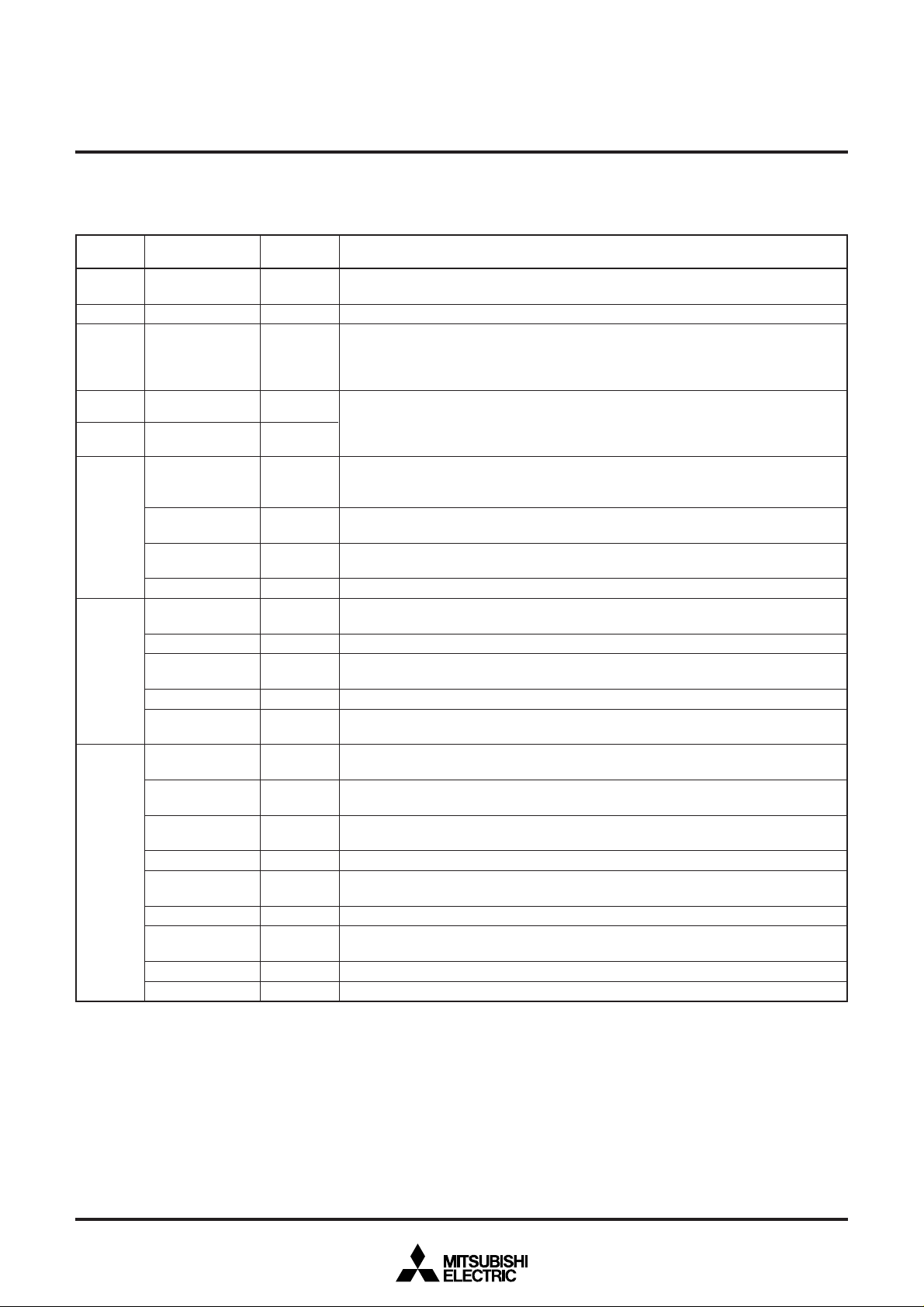
Notes 1: Port Pi (i = 0 to 3) has the port Pi direction register which can be used to program each bit as an input (“0”) or an output (“1”). The pins programmed as “1”
in the direction register are output pins. When pins are programmed as “0,” they are input pins. When pins are programmed as output pins, the output data
are written into the port latch and then output. When data is read from the output pins, the output pin level is not read but the data of the port latch is read.
This allows a previously-output value to be read correctly even if the output LOW voltage has risen, for example, because a light emitting diode was directly
driven. The input pins are in the floating state, so the values of the pins can be read. When data is written into the input pin, it is written only into the port
latch, while the pin remains in the floating state.
2: To switch output functions, set the raster color register and OSD control register. When pins P2
the corresponding bits of the port P2 direction register to “0” (input mode).
3: To switch output structures, set bits 2 and 3 of the port P3 direction register, When “0,” CMOS output ; when “1,” N-channel open-drain output.
Input/
Output
Functions
structure. (See notes 1, 3)
2–P55 are also used as OSD output pins R, G, B, OUT1 respectively. The output
6 and P27 are used as the OSD clock input/output pins, set
Rev. 1.4
8
r
r
P o r t s P 00
MITSUBISHI MICROCOMPUTERS
M37272M6/M8–XXXSP/FP, M37272MA–XXXSP
M37272E8SP/FP, M37272EFSP
SINGLE-CHIP 8-BIT CMOS MICROCOMPUTER with CLOSED CAPTION DECODER
and ON-SCREEN DISPLAY CONTROLLER
–P
05
D i r e c t i o n r e g i s t e
N-channel open-drain output
0–P05
Ports P0
D a t a b u s
P o r t s P 1 , P 2 , P 30, P 31
D a t a b u s
P o r t l a t c h
D i r e c t i o n r e g i s t e
P o r t l a t c h
Notes 1: Each port is also used as follows :
0 : OUT2
P1
1 : SCL1
P1
2 : SCL2
P1
3 : SDA15
P1
4 : SDA2
P1
5 : AD1/INT3
P1
6 : AD2
P1
7 : AD3
P1
P2
0 : SCLK
P21 : SOUT
P22 : SIN
P23 : TIM3
4 : TIM2
P2
0 : AD5
P3
1 : AD6
P3
2: The output structure of ports P3
drain output structure (when selecting N-channel open-drain, it is the same with P0
3: The output structure of ports P1
2
C-BUS interface (it is the same with P06 and P07).
I
4: The output structure of ports P2
output (it is the same as P0
Note :Each port is also used as follows :
CMOS output
Ports P1
0 and P31 can be selected either CMOS output or N-channel open-
6 and P07).
1–P14 is N-channel open-drain output when using as multi-master
0 and P21 is N-channel open-drain output when using as serial
6 and P07).
0–P05 : PWM0–PWM5
P0
, P2, P30, P31
Fig. 7.1 I/O Pin Block Diagram (1)
Rev. 1.3
9
r
MITSUBISHI MICROCOMPUTERS
M37272M6/M8–XXXSP/FP, M37272MA–XXXSP
M37272E8SP/FP, M37272EFSP
SINGLE-CHIP 8-BIT CMOS MICROCOMPUTER with CLOSED CAPTION DECODER
and ON-SCREEN DISPLAY CONTROLLER
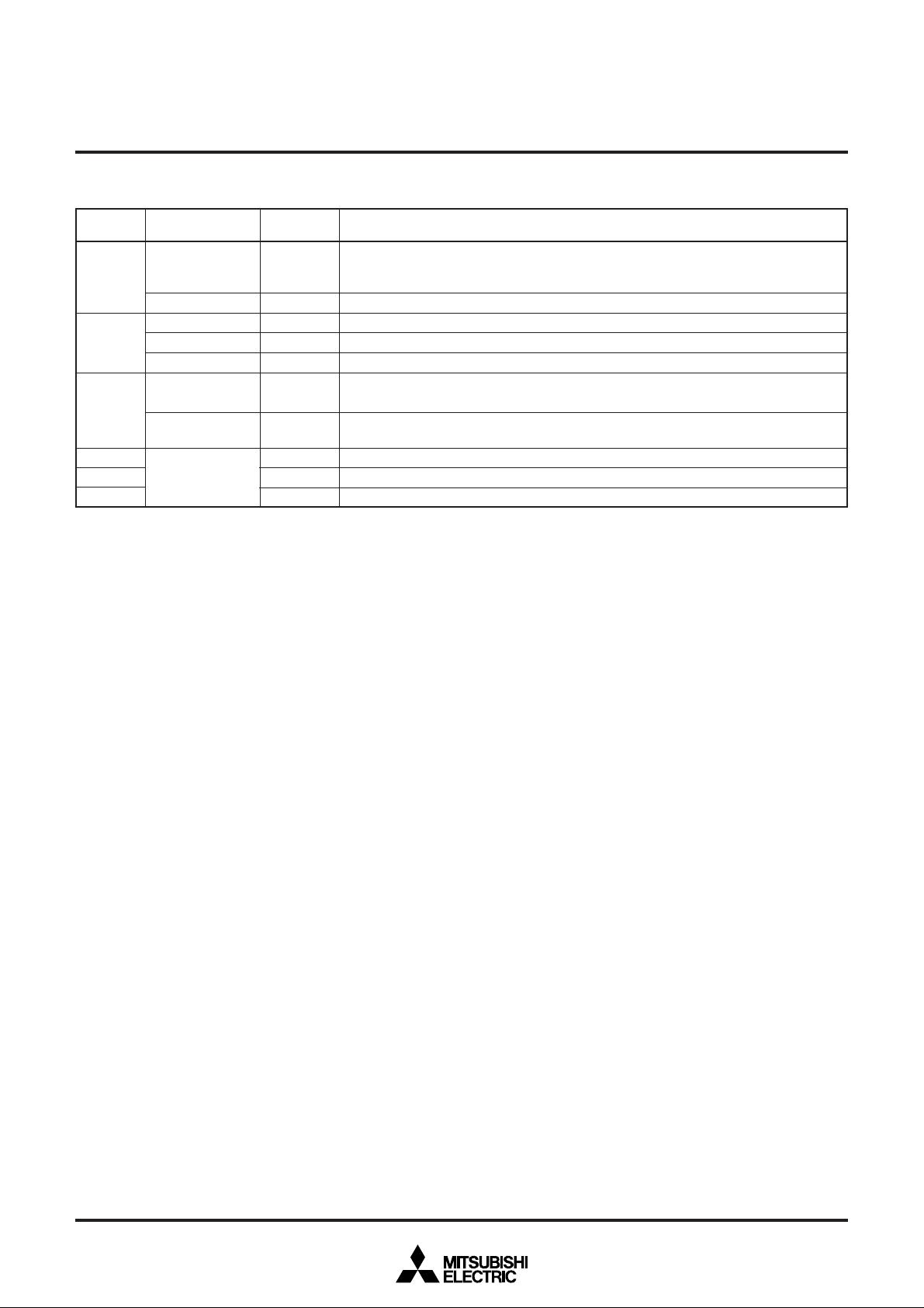
P o r t s P 06, P 0
D a t a b u s
P 50, P 5
1
I n t e r n a l c i r c u i t
7
D i r e c t i o n r e g i s t e
P o r t l a t c h
N-channel open-drain output
6, P07
Ports P0
Note :Each port is also used
as follows :
6 : INT2/AD4
P0
7 : INT1
P0
P 52– P 5
5
CMOS input
0, P51
Ports P5
Note : Each pin is also used
as follows :
0 : HSYNC
P5
P51 : VSYNC
I n t e r n a l c i r c u i t
CMOS output
2–P55
Ports P5
Note : Each pin is also used
as follows :
2 : R
P5
3 : G
P5
4 : B
P5
5 : OUT1
P5
Fig. 7.2 I/O Pin Block Diagram (2)
10
Rev. 1.4
MITSUBISHI MICROCOMPUTERS
A f t e r r e s e t
4
00516
W
W
W
7
M37272M6/M8–XXXSP/FP, M37272MA–XXXSP
M37272E8SP/FP, M37272EFSP
SINGLE-CHIP 8-BIT CMOS MICROCOMPUTER with CLOSED CAPTION DECODER
and ON-SCREEN DISPLAY CONTROLLER
8. FUNCTIONAL DESCRIPTION
8.1 CENTRAL PROCESSING UNIT (CPU)
This microcomputer uses the standard 740 Family instruction set.
Refer to the table of 740 Family addressing modes and machine
instructions or the SERIES 740 <Software> User’s Manual for details on the instruction set.
Machine-resident 740 Family instructions are as follows:
The FST, SLW instruction cannot be used.
The MUL, DIV, WIT and STP instructions can be used.
C P U M o d e R e g i s t e r
b 7b 6 b 5b 4b 3 b 2b 1b 0
1
1
C P U m o d e r e g i s t e r ( C M ) [ A d d r e s s 0 0 F B
B
P r o c e s s o r m o d e b i t s
0 , 1
N a m eF
( C M 0 , C M 1 )
8.1.1 CPU Mode Register
The CPU mode register contains the stack page selection bit and
internal system clock selection bit. The CPU mode register is allocated at address 00FB
u n c t i o n
b 1 b 0
0 0 : S i n g l e - c h i p m o d e
0 1 :
1 0 : N o t a v a i l a b l e
1 1 :
1 6
16.
]
s
RW
R
0
Fig. 8.1.1 CPU Mode Register
S t a c k p a g e s e l e c t i o n
2
b i t ( C M 2 ) ( S e e n o t e )
3 ,
F i x t h e s e b i t s t o “ 1 . ”
C O U T
d r i v a b i l i t y
X
s e l e c t i o n b i t ( C M 5 )
M a i n C l o c k ( X
s t o p b i t
( C M 6 )
I n t e r n a l s y s t e m c l o c k
s e l e c t i o n b i t
( C M 7 )
I N
– X
0 : 0 p a g e
1 : 1 p a g e
0 : L O W d r i v e
1 : H I G H d r i v e
O U T
)
0 : O s c i l l a t i n g
1 : S t o p p e d
0 : X
1 : X
I N
– X
O U T
s e l e c t e d
( h i g h - s p e e d m o d e )
C I N
– X
C O U T
s e l e c t e d
( h i g h - s p e e d m o d e )
N o t e : T h i s b i t i s s e t t o “ 1 ” a f t e r t h e r e s e t r e l e a s e .
1
RW
1
R
R
0
RW
0
RW
Rev. 1.3
11
MITSUBISHI MICROCOMPUTERS
M37272M6/M8–XXXSP/FP, M37272MA–XXXSP
M37272E8SP/FP, M37272EFSP
SINGLE-CHIP 8-BIT CMOS MICROCOMPUTER with CLOSED CAPTION DECODER
and ON-SCREEN DISPLAY CONTROLLER
8.2 MEMORY
8.2.1 Special Function Register (SFR) Area
The special function register (SFR) area in the zero page contains
control registers such as I/O ports and timers.
8.2.2 RAM
RAM is used for data storage and for stack area of subroutine calls
and interrupts.
8.2.3 ROM
ROM is used for storing user programs as well as the interrupt vector
area.
8.2.4 OSD RAM
RAM for display is used for specifying the character codes and colors to display.
8.2.5 OSD ROM
ROM for display is used for storing character data.
■ M 3 7 2 7 2 M 6 / M 8 - X X X S P / F P , M 3 7 2 7 2 E 8 S P / F P
8.2.6 Interrupt Vector Area
The interrupt vector area contains reset and interrupt vectors.
8.2.7 Zero Page
The 256 bytes from addresses 000016 to 00FF16 are called the zero
page area. The internal RAM and the special function registers (SFR)
are allocated to this area.
The zero page addressing mode can be used to specify memory and
register addresses in the zero page area. Access to this area with
only 2 bytes is possible in the zero page addressing mode.
8.2.8 Special Page
The 256 bytes from addresses FF0016 to FFFF16 are called the special page area. The special page addressing mode can be used to
specify memory addresses in the special page area. Access to this
area with only 2 bytes is possible in the special page addressing
mode.
8.2.9 ROM Correction Memory (RAM)
This is used as the program area for ROM correction.
M 3 7 2 7 2 M 6 -
X X X S P / F P
R A M
( 1 0 2 4 b y t e s )
M 3 7 2 7 2 M 8 -
X X X S P / F P ,
M 3 7 2 7 2 E 8 S P / F P
R O M
( 3 2 K b y t e s )
M 3 7 2 7 2 M 8 X X X S P / F P ,
M 3 7 2 7 2 E 8 S P / F P
R A M
( 1 1 5 2 b y t e s )
O S D R A M
( 1 2 8 b y t e s )
( S e e n o t e )
O S D R O M
( 1 0 K b y t e s )
M 3 7 2 7 2 M 6 -
X X X S P / F P
R O M
( 2 4 K b y t e s )
0 0 0 0
0 0 B F
0 0 C 0
0 0 F F
0 1 0 0
0 1 F F
0 2 0 0
0 2 0 F
0 3 0 0
0 3 2 0
0 5 3 F
0 5 B F
0 8 0 0
0 8 7 F
1 4 0 0
3 B F F
8 0 0 0
A 0 0 0
F F 0 0
F F D E
F F F F
1 6
1 6
1 6
1 6
1 6
1 6
1 6
1 6
1 6
1 6
1 6
1 6
1 6
1 6
1 6
1 6
1 6
1 6
1 6
1 6
1 6
S F R 1 a r e a
S F R 2 a r e a
N o t u s e d
N o t u s e d
N o t u s e d
N o t u s e d
I n t e r r u p t v e c t o r a r e a
Z e r o p a g e
R O M c o r r e c t i o n f u n c t i o n
V e c t o r 1 : a d d r e s s 0 3 0 0
V e c t o r 2 : a d d r e s s 0 3 2 0
S p e c i a l p a g e
1 0 0 0 0
1 6
1 6
1 6
N o t u s e d
1 F F F F
1 6
N o t e : R e f e r t o T a b l e 8 . 1 1 . 3 O S D R A M .
Fig. 8.2.1 Memory Map (M37272M6/M8-XXXSP/FP, M37272E8SP/FP)
12
Rev. 1.4
M37272M6/M8–XXXSP/FP, M37272MA–XXXSP
SINGLE-CHIP 8-BIT CMOS MICROCOMPUTER with CLOSED CAPTION DECODER
■ M 3 7 2 7 2 M A - X X X S P , M 3 7 2 7 2 E F S P
0 0 0 0
MITSUBISHI MICROCOMPUTERS
M37272E8SP/FP, M37272EFSP
and ON-SCREEN DISPLAY CONTROLLER
1 0 0 0 0
1 6
1 6
( 1 4 7 2 b y t e s )
O S D R A M
( 1 2 8 b y t e s )
( S e e n o t e )
M 3 7 2 7 2 E F S P
R O M
( 6 0 K b y t e s )
M 3 7 2 7 2 M A - X X X S P
R O M
( 4 0 K b y t e s )
R A M
0 0 B F
0 0 C 0
0 0 F F
0 1 0 0
0 1 F F
0 2 0 0
0 2 0 F
0 3 0 0
0 3 2 0
0 6 F F
0 8 0 0
0 8 7 F
1 0 0 0
6 0 0 0
F F 0 0
F F D E
F F F F
1 6
1 6
S F R 1 a r e a
1 6
1 6
1 6
1 6
S F R 2 a r e a
1 6
1 6
1 6
1 6
1 6
1 6
1 6
1 6
1 6
1 6
I n t e r r u p t v e c t o r a r e a
1 6
N o t u s e d
N o t u s e d
N o t u s e d
Z e r o p a g e
R O M c o r r e c t i o n f u n c t r i o n
V e c t o r 1 : a d d r e s s 0 3 0 0
V e c t o r 2 : a d d r e s s 0 3 2 0
O S D R O M
( 1 0 K b y t e s )
S p e c i a l p a g e
N o t u s e d
1 6
1 6
1 1 4 0 0
1 6
1 3 B F F
1 6
N o t u s e d
1 F F F F
1 6
N o t e : R e f e r t o T a b l e 8 . 1 1 . 3 O S D R A M .
Fig. 8.2.2 Memory Map (M37272MA-XXXSP, M37272EFSP)
Rev. 1.3
13
t o D
4
5
3
0
4
5
3
0
■ S F R 1 A r e a ( a d d r e s s e s C 01
A d d r e s s
C 01
C 11
C 21
C 31
C 41
C 51
C 61
C 71
C 81
C 91
C A1
C B1
C C1
C D1
C E1
C F1
D 01
D 11
D 21
D 31
D 41
D 51
D 61
D 71
D 81
D 91
D A1
D B1
D C1
D D1
D E1
D F1
6
6
6
6
6
6
6
6
6
6
6
6
6
6
6
6
6
6
6
6
6
6
6
6
6
6
6
6
6
6
6
6
R e g i s t e r
P o r t P 0 ( P 0 )
P o r t P 0 d i r e c t i o n r e g i s t e r ( D 0 )
P o r t P 1 ( P 1 )
P o r t P 1 d i r e c t i o n r e g i s t e r ( D 1 )
P o r t P 2 ( P 2 )
P o r t P 2 d i r e c t i o n r e g i s t e r ( D 2 )
P o r t P 3 ( P 3 )
P o r t P 3 d i r e c t i o n r e g i s t e r ( D 3 )
P o r t P 5 ( P 5 )
O S D p o r t c o n t r o l r e g i s t e r ( P F )
C a p t i o n d a t a r e g i s t e r 3 ( C D 3 )
C a p t i o n d a t a r e g i s t e r 4 ( C D 4 )
O S D c o n t r o l r e g i s t e r ( O C )
H o r i z o n t a l p o s i t i o n r e g i s t e r ( H P )
B l o c k c o n t r o l r e g i s t e r 1 ( B C 1 )
B l o c k c o n t r o l r e g i s t e r 2 ( B C 2 )
V e r t i c a l p o s i t i o n r e g i s t e r 1 ( V P 1 )
V e r t i c a l p o s i t i o n r e g i s t e r 2 ( V P 2 )
W i n d o w r e g i s t e r 1 ( W N 1 )
W i n d o w r e g i s t e r 2 ( W N 2 )
I / O p o l a r i t y c o n t r o l r e g i s t e r ( P C )
R a s t e r c o l o r r e g i s t e r ( R C )
I n t e r r u p t i n p u t p o l a r i t y c o n t r o l r e g i s t e r ( R E )
MITSUBISHI MICROCOMPUTERS
M37272M6/M8–XXXSP/FP, M37272MA–XXXSP
M37272E8SP/FP, M37272EFSP
SINGLE-CHIP 8-BIT CMOS MICROCOMPUTER with CLOSED CAPTION DECODER
and ON-SCREEN DISPLAY CONTROLLER
6
F1
6)
< B i t a l l o c a t i o n >
:
F u n c t i o n b i t
N a m e
:
: N o f u n c t i o n b i t
: F i x t h i s b i t t o “ 0 ”
0
< S t a t e i m m e d i a t e l y a f t e r r e s e t >
: “ 0 ” i m m e d i a t e l y a f t e r r e s e t
0
1
: “ 1 ” i m m e d i a t e l y a f t e r r e s e t
: I n d e t e r m i n a t e i m m e d i a t e l y
?
a f t e r r e s e t
( d o n o t w r i t e “ 1 ” )
: F i x t h i s b i t t o “ 1 ”
1
( d o n o t w r i t e “ 0 ” )
b 7b
B i t a l l o c a t i o nS
t a t e i m m e d i a t e l y a f t e r r e s e
0
b 7b
?
1 6
0 0
?
1 6
0 0
?
1 6
0 0
3 1
C
P 3 0P 3 1
P 3 0 DP 3 1 DP 3 0 CT 3 S CP
0 01
6
?
?
?
0 01
0 0
6
1 6
0 01
P F 2P F 3P F 4P F 5P F 7
6
00
?
0
0
O C 6
H P 6
H P
B C 1 6B C 1 7
P C 6
P C
00
C D L 2 0C D L 2 1C D L 2 2C D L 2 3C D L 2 4C D L 2 5C D L 2 6C D L 2 7
H P 1
P C 1
C D H 2 0C D H 2 1C D H 2 2C D H 2 3C D H 2 4C D H 2 5C D H 2 6C D H 2 7
C 0O C
1
H P
B C 1 0B C 1 1
B C 2 0B C 2 1B C 2 2B C 2 3B C 2 4B C 2 5B C 2 6B C 2 7
V P 1 0V P 1 1V P 1 2V P 1 3V P 1 4V P 1 5V P 1 6V P 1 7
V P 2 0V P 2 1V P 2 2V P 2 3V P 2 4V P 2 5V P 2 6V P 2 7
W N 1 0W N 1 1W N 1 2W N 1 3W N 1 4W N 1 5W N 1 6W N 1 7
W N 2 0W N 2 1W N 2 2W N 2 3W N 2 4W N 2 5W N 2 6W N 2 7
P C
R C 0R C 1R C 2R C 7
O C 4O C 5O
H P
P C
C 2O C
3O
H P 2H P
B C 1 2B C 1 3B C 1 4B C 1 5
P C 2P C
R C 3R C 4
?
?
0 01
0 01
?
?
?
?
?
?
4 01
0 01
6
6
6
6
?
?
0 01
0 01
0 01
S e e n o t
0 01
6
6
6
6 (
0 01
0 01
S e e n o t
0 0
I N T 1I N T 2I N T 3
6
6
1
6 (
e 1)
e 2 )
t
0
??000000
N o t e s 1: T h i s i s o n l y M 3 7 2 7 2 M A - X X X S P a n d M 3 7 2 7 2 E F S P .
2: A s f o r M 3 7 2 7 2 M 6 / M 8 - X X X S P / F P a n d M 3 7 2 7 2 E 8 S P / F P , t h e r e s e t v a l u e i s ? ( i n d e t e r m i n a t e ) .
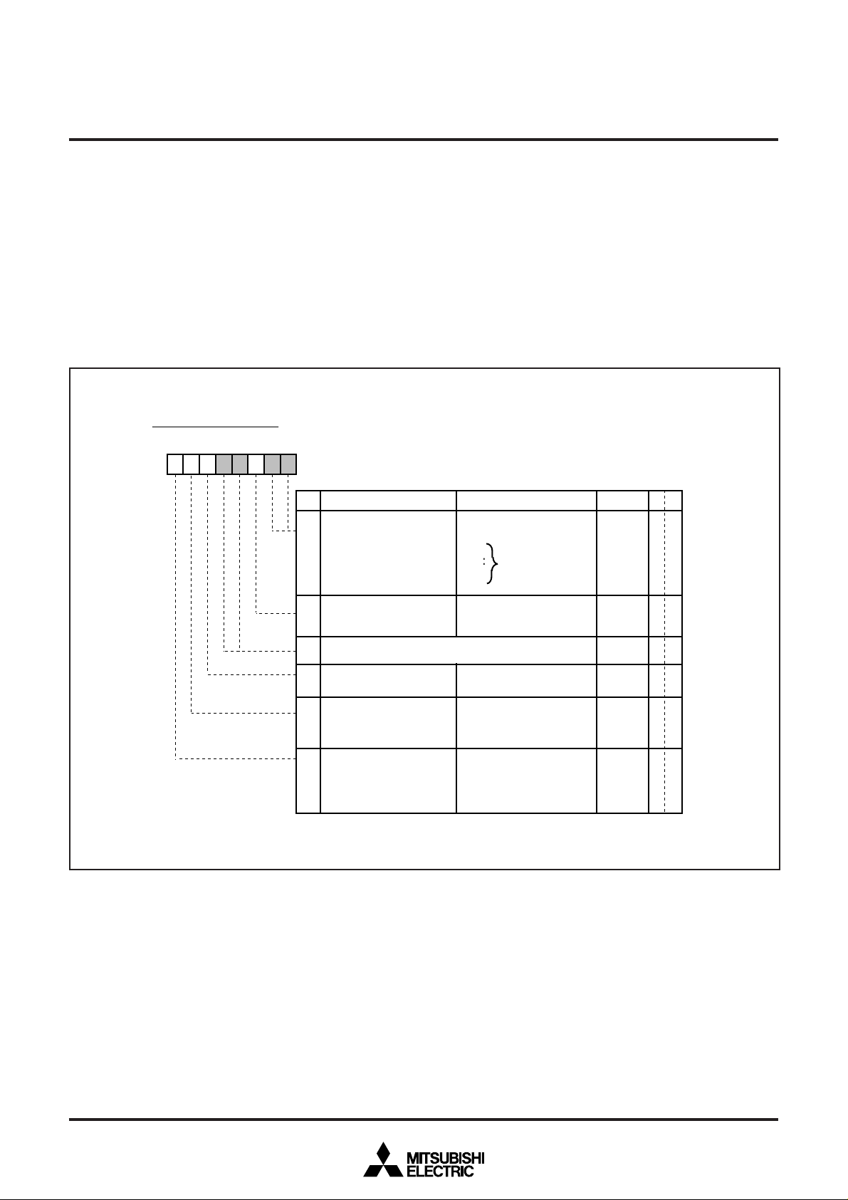
Fig. 8.2.3 Memory Map of Special Function Register 1 (SFR1) (1)
Rev. 1.4
14
MITSUBISHI MICROCOMPUTERS
6
6
6
6
6
6
6
6
6
6
6
6
6
R
M37272M6/M8–XXXSP/FP, M37272MA–XXXSP
M37272E8SP/FP, M37272EFSP
SINGLE-CHIP 8-BIT CMOS MICROCOMPUTER with CLOSED CAPTION DECODER
and ON-SCREEN DISPLAY CONTROLLER
■ S F R 1 A r e a ( a d d r e s s e s E 0
A d d r e s s
E 01
6
E 11
6
E 21
6
E 31
6
E 41
6
E 51
6
E 61
6
E 71
6
E 81
6
E 91
6
E A1
6
E B1
6
E C1
E D1
E E1
6
E F1
F 01
F 11
F 21
F 31
F 41
F 51
F 61
F 71
F 81
F 91
F A1
6
F B1
6
F C1
6
F D1
6
F E1
6
F F1
6
R e g i s t e r
D a t a s l i c e r c o n t r o l r e g i s t e r 1 ( D S C 1 )
D a t a s l i c e r c o n t r o l r e g i s t e r 2 ( D S C 2 )
C a p t i o n d a t a r e g i s t e r 1 ( C D 1 )
C a p t i o n d a t a r e g i s t e r 2 ( C D 2 )
C l o c k r u n - i n d e t e c t r e g i s t e r ( C R D )
D a t a c l o c k p o s i t i o n r e g i s t e r ( D P S )
C a p t i o n p o s i t i o n r e g i s t e r ( C P S )
D a t a s l i c e r t e s t r e g i s t e r 2
D a t a s l i c e r t e s t r e g i s t e r 1
S y n c h r o n o u s s i g n a l c o u n t e r r e g i s t e r ( H C )
S e r i a l I / O r e g i s t e r ( S I O )
S e r i a l I / O m o d e r e g i s t e r ( S M )
A - D c o n t r o l r e g i s t e r 1 ( A D 1 )
A - D c o n t r o l r e g i s t e r 2 ( A D 2 )
T i m e r 5 ( T 5 )
T i m e r 6 ( T 6 )
T i m e r 1 ( T 1 )
T i m e r 2 ( T 2 )
T i m e r 3 ( T 3 )
T i m e r 4 ( T 4 )
T i m e r m o d e r e g i s t e r 1 ( T M 1 )
T i m e r m o d e r e g i s t e r 2 ( T M 2 )
2
I
C d a t a s h i f t r e g i s t e r ( S 0 )
2
I
C a d d r e s s r e g i s t e r ( S 0 D )
2
I
C s t a t u s r e g i s t e r ( S 1 )
2
I
C c o n t r o l r e g i s t e r ( S 1 D )
2
I
C c l o c k c o n t r o l r e g i s t e r ( S 2 )
C P U m o d e r e g i s t e r ( C P U M )
I n t e r r u p t r e q u e s t r e g i s t e r 1 ( I R E Q 1 )
I n t e r r u p t r e q u e s t r e g i s t e r 2 ( I R E Q 2 )
I n t e r r u p t c o n t r o l r e g i s t e r 1 ( I C O N 1 )
I n t e r r u p t c o n t r o l r e g i s t e r 2 ( I C O N 2 )
1 6
t o F F
< B i t a l l o c a t i o n >
N a m e
0
1 6
)
:
F u n c t i o n b i t
:
: N o f u n c t i o n b i t
: F i x t h i s b i t t o “ 0 ”
< S t a t e i m m e d i a t e l y a f t e r r e s e t >
: “ 0 ” i m m e d i a t e l y a f t e r r e s e t
0
: “ 1 ” i m m e d i a t e l y a f t e r r e s e t
1
: I n d e t e r m i n a t e i m m e d i a t e l y
?
a f t e r r e s e t
( d o n o t w r i t e “ 1 ” )
: F i x t h i s b i t t o “ 1 ”
1
( d o n o t w r i t e “ 0 ” )
b 7b
B i t a l l o c a t i o nS
01100
01
T M 2 6T M 2 7
B S E L 0B S E L 1
A C K
B I T
I N 3 R
T M 5 6 R
I N 3 E
T M 5 6 ET M 5 6 C
S M 5S M 6
T M 1 5T M 1 6T M 1 7
T M 2 5
1 0 B I T
S A D
F A S T
M O D E
00
C M 7C M 5C M 6
D S C 2 3D S C 2 4D S C 2 5
C R D 3C R D 4C R D 5C R D 6C R D 7
D P S 3D P S 4D P S 5D P S 6D P S 7
A D C 2 4A D C 2 3
101
C K 0 I N 1 R
C K
I N 2 RI I C R
C K EI I C E
D L 1 1C D L 1
2C D L 1 6C D L 1 7
D H 1 1C D H 1
2C D H 1 6C D H 1 7
1
P S 1C P S
2C P S 6C P S 7
C 1H C
2
D 1D 2D 3D 4D 5D 6D 7D
S A D 0S A D 1S A D 2S A D 3S A D 4S A D 5S A D 6R
C M 2
D S R
S 1 R
t a t e i m m e d i a t e l y a f t e r r e s e
b 7b
0
D S C 1 0D S C 1 1D S C 1 2
D S C 2 0
C D L 1 0C D L 1 3C D L 1 4C D L 1 5C
C D H 1 0C D H 1 3C D H 1 4C D H 1 5C
00
C P S 0C P S 3C P S 4C P S 5C
H C 0H C 3H C 4H C 5H
S M 0S M 1S M 2S M 3
A D C 1 0A D C 1 1A D C 1 2A D C 1 4
A D C 2 0A D C 2 1A D C 2 2A D C 2 5
T M 1 0T M 1 1T M 1 2T M 1 3T M 1 4
T M 2 0T M 2 1T M 2 2T M 2 3T M 2 4
0
B
W
L R BA D 0A A SA LP I NB BT R XM S T
B C 0B C 1B C 2E S OA L S
C C R 0C C R 1C C R 2C C R 3C C R 4A C K
00
T M 1 RT M 2 RT M 3 RT M 4 RO S D RV S C R
T M 1 ET M 2 ET M 3 ET M 4 EO S D EV S C E
I N 1 ED S ES 1 EI N 2 E
0?0? 0???
0 01
6
0 01
6
0 01
6
0 01
6
0 91
6
0 01
6
0 01
6
0 01
6
?
0 01
6
0000
?
0 01
6
0 71
6
F F1
6
F F1
6
0 71
6
F F1
6
0 71
6
0 01
6
0 01
6
?
0 01
6
0 01
0 01
3 C1
0 01
0 01
0 01
0 01
00 0 010 0?
6
6
6
6
6
6
6
t
0
0000?00 0
000
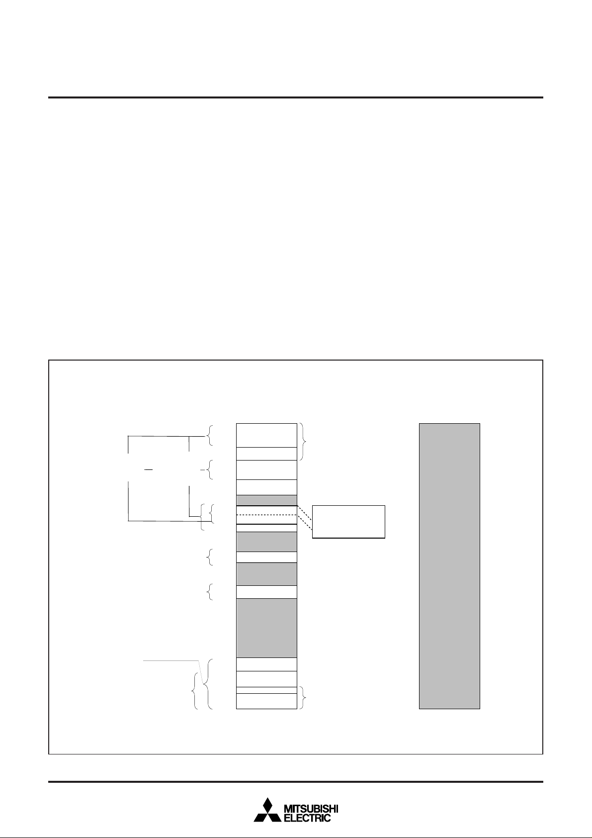
Fig. 8.2.4 Memory Map of Special Function Register 1 (SFR1) (2)
Rev. 1.3
15
MITSUBISHI MICROCOMPUTERS
6
6
6
6
6
6
6
6
6
6
6
M37272M6/M8–XXXSP/FP, M37272MA–XXXSP
M37272E8SP/FP, M37272EFSP
SINGLE-CHIP 8-BIT CMOS MICROCOMPUTER with CLOSED CAPTION DECODER
and ON-SCREEN DISPLAY CONTROLLER
■ S F R 2 A r e a ( a d d r e s s e s 2 0 0
A d d r e s s
2 0 0
1
2 0 1
1
2 0 2
1
2 0 3
1
2 0 4
1
2 0 5
1
2 0 6
1
2 0 7
1
2 0 8
1
2 0 9
1
2 0 A
1 6
2 0 B
1 6
2 0 C
1 6
2 0 D
1 6
2 0 E
1 6
2 0 F
1
P W M 0 r e g i s t e r ( P W M 0 )
P W M 1 r e g i s t e r ( P W M 1 )
P W M 2 r e g i s t e r ( P W M 2 )
P W M 3 r e g i s t e r ( P W M 3 )
P W M 4 r e g i s t e r ( P W M 4 )
P W M 5 r e g i s t e r ( P W M 5 )
P W M m o d e r e g i s t e r 1 ( P M 1 )
P W M m o d e r e g i s t e r 2 ( P M 2 )
R O M c o r r e c t i o n a d d r e s s 1 ( h i g h - o r d e r )
R O M c o r r e c t i o n a d d r e s s 1 ( l o w - o r d e r )
R O M c o r r e c t i o n a d d r e s s 2 ( h i g h - o r d e r )
O M c o r r e c t i o n a d d r e s s 2 ( l o w - o r d e r
R
O M c o r r e c t i o n e n a b l e r e g i s t e r ( R C R
R
R e g i s t e r
)
1 6
t o 2 0 F
< B i t a l l o c a t i o n >
:
N a m e
:
: N o f u n c t i o n b i t
: F i x t h i s b i t t o “ 0 ”
0
( d o n o t w r i t e “ 1 ” )
: F i x t h i s b i t t o “ 1 ”
1
( d o n o t w r i t e “ 0 ” )
b 7b
1 6
)
< S t a t e i m m e d i a t e l y a f t e r r e s e t >
: “ 0 ” i m m e d i a t e l y a f t e r r e s e t
F u n c t i o n b i t
B i t a l l o c a t i o nS
0
1
: “ 1 ” i m m e d i a t e l y a f t e r r e s e t
: I n d e t e r m i n a t e i m m e d i a t e l y
?
a f t e r r e s e t
t a t e i m m e d i a t e l y a f t e r r e s e
0
b 7b
?
?
?
?
?
?
0 0
00
)
1 6
1 6
0 0
P M 1 3
P M 2 5P M 2 4P M 2 3P M 2 2P M 2 1P M 2 0
P M 1 0
R C 0R C 1
? ???0 ?? 0
0 0
0 0
0 0
0 0
0 0
0 0
?
?
1 6
1 6
1 6
1 6
1 6
1 6
?
t
0
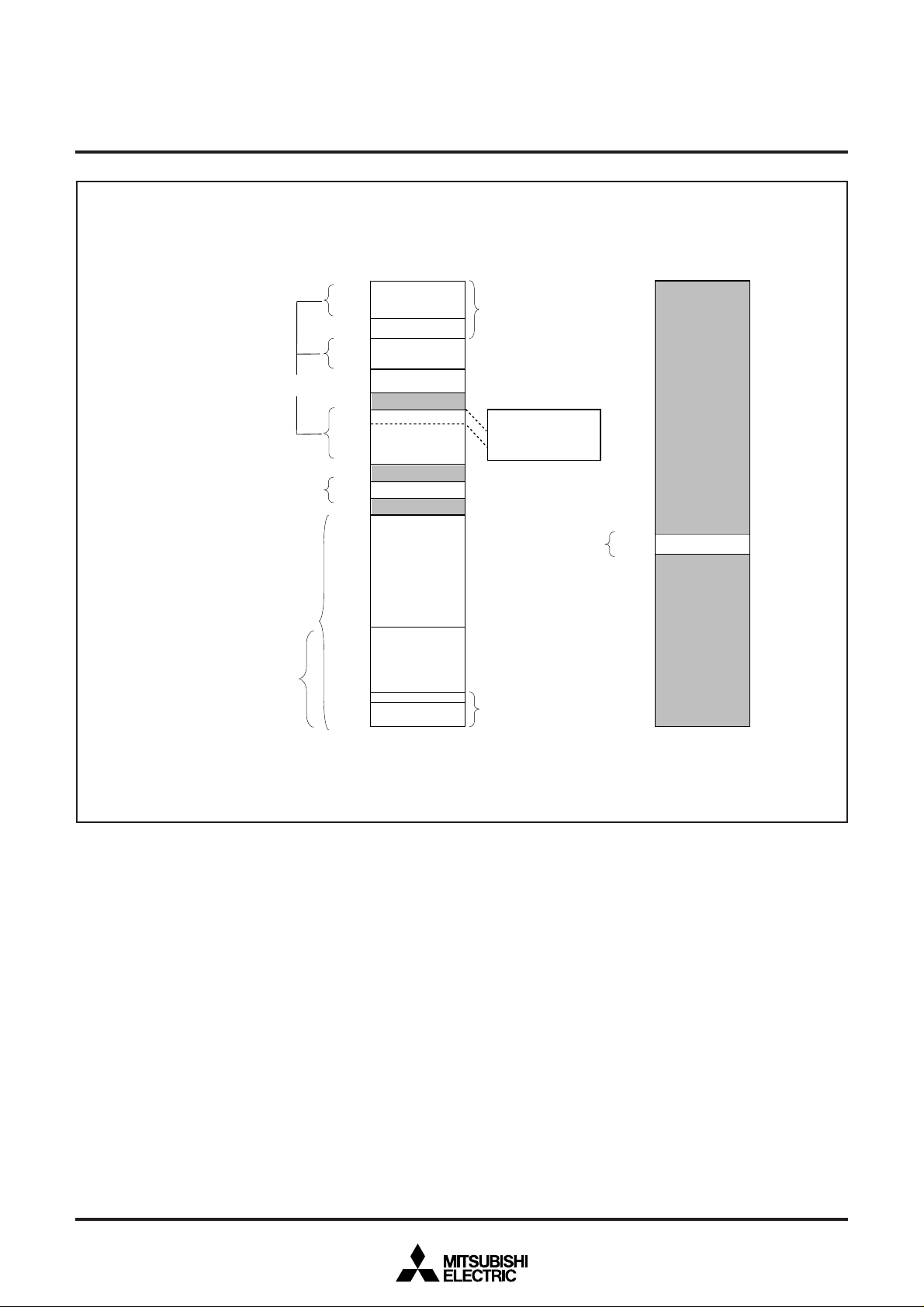
Fig. 8.2.5 Memory Map of Special Function Register 2 (SFR2)
16
Rev. 1.3
R e g i s t e r
P r o c e s s o r s t a t u s r e g i s t e r ( P S )
P r o g r a m c o u n t e r ( P CH)
P r o g r a m c o u n t e r ( P CL)
MITSUBISHI MICROCOMPUTERS
M37272M6/M8–XXXSP/FP, M37272MA–XXXSP
M37272E8SP/FP, M37272EFSP
SINGLE-CHIP 8-BIT CMOS MICROCOMPUTER with CLOSED CAPTION DECODER
and ON-SCREEN DISPLAY CONTROLLER
<
<
B i t a l l o c a t i o n
:
:
N a m e
:
N o f u n c t i o n b i t
: F i x t o t h i s b i t t o “ 0 ”
0
>
F u n c t i o n b i t
( d o n o t w r i t e t o “ 1 ” )
: F i x t o t h i s b i t t o “ 1 ”
1
( d o n o t w r i t e t o “ 0 ” )
B i t a l l o c a t i o nS
b 7
0
1
?
b 0
b 7
I Z CDBTVN???????
S t a t e i m m e d i a t e l y a f t e r r e s e t
: “ 0 ” i m m e d i a t e l y a f t e r r e s e t
: “ 1 ” i m m e d i a t e l y a f t e r r e s e t
: I n d e t e r m i n a t e i m m e d i a t e l y
a f t e r r e s e t
t a t e i m m e d i a t e l y a f t e r r e s e
1
C o n t e n t s o f a d d r e s s F F F F
C o n t e n t s o f a d d r e s s F F F E
>
t
b 0
1 6
1 6
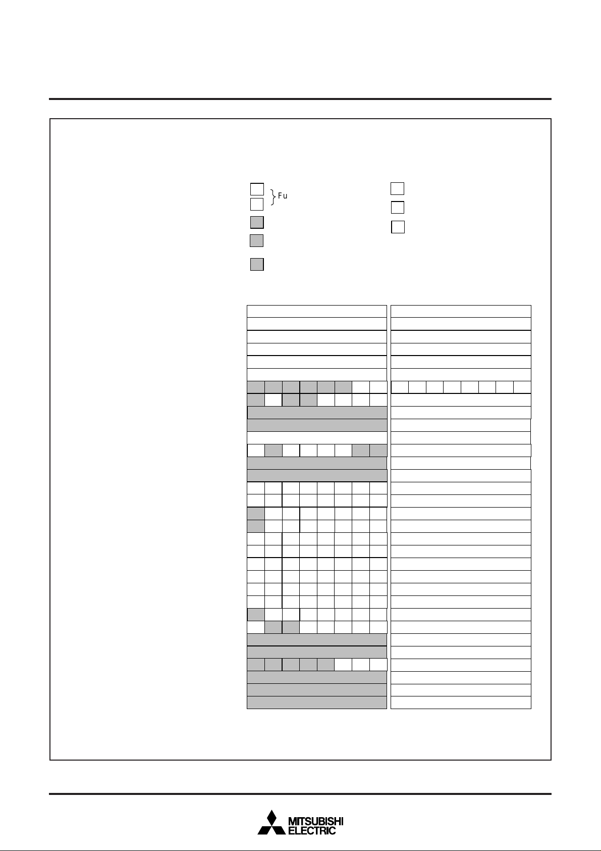
Fig. 8.2.6 Internal State of Processor Status Register and Program Counter at Reset
Rev. 1.3
17
MITSUBISHI MICROCOMPUTERS
M37272M6/M8–XXXSP/FP, M37272MA–XXXSP
M37272E8SP/FP, M37272EFSP
SINGLE-CHIP 8-BIT CMOS MICROCOMPUTER with CLOSED CAPTION DECODER
and ON-SCREEN DISPLAY CONTROLLER
8.3 INTERRUPTS
Interrupts can be caused by 17 different sources consisting of 4 external, 11 internal, 1 software, and reset. Interrupts are vectored interrupts with priorities as shown in T able 8.3.1. Reset is also included
in the table because its operation is similar to an interrupt.
When an interrupt is accepted,
① The contents of the program counter and processor status regis-
ter are automatically stored into the stack.
➁ The interrupt disable flag I is set to “1” and the corresponding
interrupt request bit is set to “0.”
➂ The jump destination address stored in the vector address enters
the program counter.
Other interrupts are disabled when the interrupt disable flag is set to
“1.”
All interrupts except the BRK instruction interrupt have an interrupt
request bit and an interrupt enable bit. The interrupt request bits are
in interrupt request registers 1 and 2 and the interrupt enable bits are
in interrupt control registers 1 and 2. Figures 8.3.2 to 8.3.6 show the
interrupt-related registers.
Interrupts other than the BRK instruction interrupt and reset are accepted when the interrupt enable bit is “1,” interrupt request bit is “1,”
and the interrupt disable flag is “0.” The interrupt request bit can be
set to “0” by a program, but not set to “1.” The interrupt enable bit can
be set to “0” and “1” by a program.
Reset is treated as a non-maskable interrupt with the highest priority.
Figure 8.3.1 shows interrupt control.
8.3.1 Interrupt Causes
(1) V
SYNC, OSD interrupts
The VSYNC interrupt is an interrupt request synchronized with
the vertical sync signal.
The OSD interrupt occurs after character block display to the
CRT is completed.
(2) INT1 to INT3 external interrupts
The INT1 to INT3 interrupts are external interrupt inputs, the system detects that the level of a pin changes from LOW to HIGH or
from HIGH to LOW, and generates an interrupt request. The input active edge can be selected by bits 3 to 5 of the interrupt
input polarity register (address 00DC
change from LOW to HIGH is detected; when it is “1,” a change
from HIGH to LOW is detected. Note that both bits are cleared to
“0” at reset.
16) : when this bit is “0,” a
(3) Timers 1 to 4 interrupts
An interrupt is generated by an overflow of timers 1 to 4.
Table 8.3.1 Interrupt Vector Addresses and Priority
Priority
1
Reset
2
OSD interrupt
3
INT1 external interrupt
4
Data slicer interrupt
5
Serial I/O interrupt
6
Timer 4 interrupt
7
f(X
IN)/4096 interrupt
8
V
SYNC interrupt
9
Timer 3 interrupt
10
Timer 2 interrupt
11
Timer 1 interrupt
12
INT3 external interrupt
13
INT2 external interrupt
14
Multi-master I
15
Timer 5 • 6 interrupt
16
BRK instruction interrupt
Note: Switching a source during a program causes an unnecessary interrupt. Therefore, set a source at initializing of program.
Interrupt Source
2
C-BUS interface interrupt
Vector Addresses
FFFF
16, FFFE16
FFFD16, FFFC16
FFFB16, FFFA16
FFF916, FFF816
FFF716, FFF616
FFF516, FFF416
FFF316, FFF216
FFF116, FFF016
FFEF16, FFEE16
FFED16, FFEC16
FFEB16, FFEA16
FFE916, FFE816
FFE716, FFE616
FFE516, FFE416
FFE316, FFE216
FFDF16, FFDE16
Non-maskable
Active edge selectable
Active edge selectable
Active edge selectable
Source switch by software (see note)
Non-maskable
Remarks
18
Rev. 1.3
M37272M6/M8–XXXSP/FP, M37272MA–XXXSP
t
SINGLE-CHIP 8-BIT CMOS MICROCOMPUTER with CLOSED CAPTION DECODER
(4) Serial I/O interrupt
This is an interrupt request from the clock synchronous serial I/O
function.
(5) f(XIN)/4096 interrupt
The f (XIN)/4096 interrupt occurs regularly with a f(XIN)/4096 period. Set bit 0 of the PWM mode register 1 to “0.”
(6) Data slicer interrupt
An interrupt occurs when slicing data is completed.
(7) Multi-master I2C-BUS interface interrupt
This is an interrupt request related to the multi-master I2C-BUS
interface.
MITSUBISHI MICROCOMPUTERS
M37272E8SP/FP, M37272EFSP
and ON-SCREEN DISPLAY CONTROLLER
I n t e r r u p t r e q u e s t b i
I n t e r r u p t e n a b l e b i t
I n t e r r u p t d i s a b l e f l a g I
B R K i n s t r u c t i o n
R e s e t
I n t e r r u p t
r e q u e s t
(8) Timer 5 • 6 interrupt
An interrupt is generated by an overflow of timer 5 or 6. Their
priorities are same, and can be switched by software.
(9) BRK instruction interrupt
This software interrupt has the least significant priority. It does
not have a corresponding interrupt enable bit, and it is not affected by the interrupt disable flag I (non-maskable).
Fig. 8.3.1 Interrupt Control
Rev. 1.3
19
M37272M6/M8–XXXSP/FP, M37272MA–XXXSP
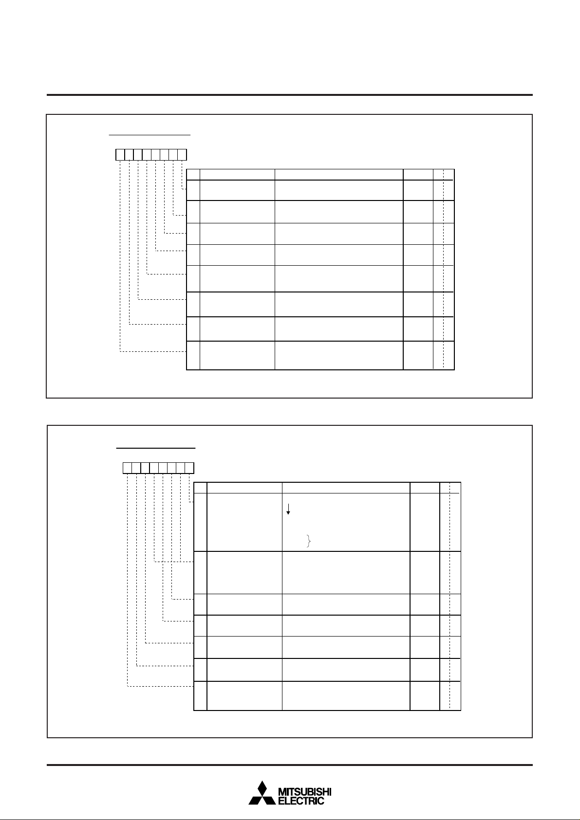
6
5
W
6
I n t e r r u p t R e q u e s t R e g i s t e r 1
b 7b 6 b 5b 4b 3 b 2b 1b 0
I n t e r r u p t r e q u e s t r e g i s t e r 1 ( I R E Q 1 ) [ A d d r e s s 0 0 F C
BN
0
1T i m e r 2 i n t e r r u p t
2T i m e r 3 i n t e r r u p t
3
4O S D i n t e r r u p t r e q u e s t
5V
6
7
MITSUBISHI MICROCOMPUTERS
M37272E8SP/FP, M37272EFSP
SINGLE-CHIP 8-BIT CMOS MICROCOMPUTER with CLOSED CAPTION DECODER
and ON-SCREEN DISPLAY CONTROLLER
1 6
]
a m
eF
T i m e r 1 i n t e r r u p t
r e q u e s t b i t ( T M 1 R )
r e q u e s t b i t ( T M 2 R )
r e q u e s t b i t ( T M 3 R )
T i m e r 4 i n t e r r u p t
r e q u e s t b i t ( T M 4 R )
b i t ( O S D R )
S Y N C
i n t e r r u p t
r e q u e s t b i t ( V S C R )
I N T 3 e x t e r n a l i n t e r r u p t
r e q u e s t b i t ( V S C R )
N o t h i n g i s a s s i g n e d . T h i s b i t i s a w r i t e d i s a b l e b i t .
W h e n t h i s b i t i s r e a d o u t , t h e v a l u e i s “ 0 . ”
u n c t i o n
s
0 : N o i n t e r r u p t r e q u e s t i s s u e d
1 : I n t e r r u p t r e q u e s t i s s u e d
0 : N o i n t e r r u p t r e q u e s t i s s u e d
1 : I n t e r r u p t r e q u e s t i s s u e d
0 : N o i n t e r r u p t r e q u e s t i s s u e d
1 : I n t e r r u p t r e q u e s t i s s u e d
0 : N o i n t e r r u p t r e q u e s t i s s u e d
1 : I n t e r r u p t r e q u e s t i s s u e d
0 : N o i n t e r r u p t r e q u e s t i s s u e d
1 : I n t e r r u p t r e q u e s t i s s u e d
0 : N o i n t e r r u p t r e q u e s t i s s u e d
1 : I n t e r r u p t r e q u e s t i s s u e d
0 : N o i n t e r r u p t r e q u e s t i s s u e d
1 : I n t e r r u p t r e q u e s t i s s u e d
A f t e r r e s e t
0
0
0
0
0
0
0
0
RW
R
✽
R
✽
R
✽
R
✽
R
✽
R
✽
R
✽
—
R
Fig. 8.3.2 Interrupt Request Register 1
I n t e r r u p t R e q u e s t R e g i s t e r 2
b 7b
b 5b 4b 3 b 2b 1b 0
0
✽: “ 0 ” c a n b e s e t b y s o f t w a r e , b u t “ 1 ” c a n n o t b e s e t .
I n t e r r u p t r e q u e s t r e g i s t e r 2 ( I R E Q 2 ) [ A d d r e s s 0 0 F D
BN
0
a m
eF
I N T 1 e x t e r n a l i n t e r r u p t
r e q u e s t b i t ( I N I R )
D a t a s l i c e r i n t e r r u p t
1
r e q u e s t b i t ( D S R )
2
S e r i a l I / O i n t e r r u p t
r e q u e s t b i t ( S 1 R )
/ 4 0 9 6 i n t e r r u p t
f ( XI
N)
3
r e q u e s t b i t ( C K R )
4
I N T 2 e x t e r n a l i n t e r r u p t
r e q u e s t b i t ( I N 2 R )
2
M u l t i - m a s t e r I
C - B U S
i n t e r r u p t r e q u e s t b i t ( I I C R )
T i m e r 5 • 6 i n t e r r u p t
r e q u e s t b i t ( T M 5 6 R )
u n c t i o n
0 : N o i n t e r r u p t r e q u e s t i s s u e d
1 : I n t e r r u p t r e q u e s t i s s u e d
0 : N o i n t e r r u p t r e q u e s t i s s u e d
1 : I n t e r r u p t r e q u e s t i s s u e d
0 : N o i n t e r r u p t r e q u e s t i s s u e d
1 : I n t e r r u p t r e q u e s t i s s u e d
0 : N o i n t e r r u p t r e q u e s t i s s u e d
1 : I n t e r r u p t r e q u e s t i s s u e d
0 : N o i n t e r r u p t r e q u e s t i s s u e d
1 : I n t e r r u p t r e q u e s t i s s u e d
0 : N o i n t e r r u p t r e q u e s t i s s u e d
1 : I n t e r r u p t r e q u e s t i s s u e d
0 : N o i n t e r r u p t r e q u e s t i s s u e d
1 : I n t e r r u p t r e q u e s t i s s u e d
7F i x t h i s b i t t o “ 0 . ”
1 6]
s
A f t e r r e s e t
0
0
0
0
0
0
0
0
RW
R
✽
R
✽
R
✽
R
✽
R
✽
R
✽
R
✽
R
✽: “ 0 ” c a n b e s e t b y s o f t w a r e , b u t “ 1 ” c a n n o t b e s e t .
Fig. 8.3.3 Interrupt Request Register 2
Rev. 1.3
20
M37272M6/M8–XXXSP/FP, M37272MA–XXXSP
7
5
6
5
6
7
SINGLE-CHIP 8-BIT CMOS MICROCOMPUTER with CLOSED CAPTION DECODER
I n t e r r u p t C o n t r o l R e g i s t e r 1
b 7b 6 b 5b 4b 3 b 2b 1b 0
I n t e r r u p t c o n t r o l r e g i s t e r 1 ( I C O N 1 ) [ A d d r e s s 0 0 F E
BN
0
1
2
3
4
MITSUBISHI MICROCOMPUTERS
M37272E8SP/FP, M37272EFSP
and ON-SCREEN DISPLAY CONTROLLER
a m
eF
T i m e r 1 i n t e r r u p t
e n a b l e b i t ( T M 1 E )
T i m e r 2 i n t e r r u p t
e n a b l e b i t ( T M 2 E )
T i m e r 3 i n t e r r u p t
e n a b l e b i t ( T M 3 E )
T i m e r 4 i n t e r r u p t
e n a b l e b i t ( T M 4 E )
O S D i n t e r r u p t e n a b l e b i t
( O S D E )
V
S Y N C
i n t e r r u p t e n a b l e
b i t ( V S C E )
I N T 3 e x t e r n a l i n t e r r u p t
e n a b l e b i t ( I N 3 E )
N o t h i n g i s a s s i g n e d . T h i s b i t i s a w r i t e d i s a b l e
b i t . W h e n t h i s b i t i s r e a d o u t , t h e v a l u e i s “ 0 . ”
u n c t i o n
0 : I n t e r r u p t d i s a b l e d
1 : I n t e r r u p t e n a b l e d
0 : I n t e r r u p t d i s a b l e d
1 : I n t e r r u p t e n a b l e d
0 : I n t e r r u p t d i s a b l e d
1 : I n t e r r u p t e n a b l e d
0 : I n t e r r u p t d i s a b l e d
1 : I n t e r r u p t e n a b l e d
0 : I n t e r r u p t d i s a b l e d
1 : I n t e r r u p t e n a b l e d
0 : I n t e r r u p t d i s a b l e d
1 : I n t e r r u p t e n a b l e d
0 : I n t e r r u p t d i s a b l e d
1 : I n t e r r u p t e n a b l e d
s
1 6
]
A f t e r r e s e t
0
0
0
0
0
0RW
0RW
0
RW
RW
RW
RW
RW
RW
R—
Fig. 8.3.4 Interrupt Control Register 1
I n t e r r u p t C o n t r o l R e g i s t e r 2
b 7b 6 b 5b 4b 3 b 2b 1b 0
I n t e r r u p t c o n t r o l r e g i s t e r 2 ( I C O N 2 ) [ A d d r e s s 0 0 F F
BN
I N T 1 e x t e r n a l i n t e r r u p t
0
e n a b l e b i t ( I N 1 E )
D a t a s l i c e r i n t e r r u p t
1
e n a b l e b i t ( D S E )
S e r i a l I / O i n t e r r u p t
2
e n a b l e b i t ( S 1 E )
f ( X
3
e n a b l e b i t ( C K E )
I N T 2 e x t e r n a l i n t e r r u p t
4
e n a b l e b i t ( I N 2 E )
M u l t i - m a s t e r I2C - B U S
i n t e r f a c e i n t e r r u p t e n a b l e
b i t ( I I C E )
T i m e r 5 • 6 i n t e r r u p t
e n a b l e b i t ( T M 5 6 E )
T i m e r 5 • 6 i n t e r r u p t
s w i t c h b i t ( T M 5 6 C )
a m
eF
I N
) / 4 0 9 6 i n t e r r u p t
u n c t i o n
0 : I n t e r r u p t d i s a b l e d
1 : I n t e r r u p t e n a b l e d
0 : I n t e r r u p t d i s a b l e d
1 : I n t e r r u p t e n a b l e d
0 : I n t e r r u p t d i s a b l e d
1 : I n t e r r u p t e n a b l e d
0 : I n t e r r u p t d i s a b l e d
1 : I n t e r r u p t e n a b l e d
0 : I n t e r r u p t d i s a b l e d
1 : I n t e r r u p t e n a b l e d
0 : I n t e r r u p t d i s a b l e d
1 : I n t e r r u p t e n a b l e d
0 : I n t e r r u p t d i s a b l e d
1 : I n t e r r u p t e n a b l e d
0 : T i m e r 5
1 : T i m e r 6
s
1 6
]
A f t e r r e s e t
0
0
0
0
0
0RW
0RW
0RW
RW
RW
RW
RW
RW
RW
Fig. 8.3.5 Interrupt Control Register 2
Rev. 1.3
21
M37272M6/M8–XXXSP/FP, M37272MA–XXXSP
SINGLE-CHIP 8-BIT CMOS MICROCOMPUTER with CLOSED CAPTION DECODER
Interrupt Input Polarity Register
b7 b6 b5 b4 b3 b2 b1 b0
Interrupt input polarity register (RE) [Address 00DC
B Name Functions After reset R W
INT1 polarity switch bit
0
(INT1)
INT2 polarity switch bit
4
(INT2)
INT3 polarity switch bit
5
(INT3)
4
Nothing is assigned. These bits are write disable bits.
to
When these bits are read out, the values are “0.”
7
MITSUBISHI MICROCOMPUTERS
M37272E8SP/FP, M37272EFSP
and ON-SCREEN DISPLAY CONTROLLER
16
]
0
0 : Positive polarity
1 : Negative polarity
0 : Positive polarity
1 : Negative polarity
0 : Positive polarity
1 : Negative polarity
RW
0
RW
0
RW
0
R—
Fig. 8.3.6 Interrupt Input Polarity Register
22
Rev. 1.3

MITSUBISHI MICROCOMPUTERS
M37272M6/M8–XXXSP/FP, M37272MA–XXXSP
M37272E8SP/FP, M37272EFSP
SINGLE-CHIP 8-BIT CMOS MICROCOMPUTER with CLOSED CAPTION DECODER
and ON-SCREEN DISPLAY CONTROLLER
8.4 TIMERS
This microcomputer has 6 timers: timer 1, timer 2, timer 3, timer 4,
timer 5, and timer 6. All timers are 8-bit timers with the 8-bit timer
latch. The timer block diagram is shown in Figure 8.4.3.
All of the timers count down and their divide ratio is 1/(n+1), where n
is the value of timer latch. By writing a count value to the corresponding timer latch (addresses 00F016 to 00F316 : timers 1 to 4, addresses
00EE16 and 00EF16 : timers 5 and 6), the value is also set to a timer,
simultaneously.
The count value is decremented by 1. The timer interrupt request bit
is set to “1” by a timer overflow at the next count pulse, after the
count value reaches “0016”.
8.4.1 Timer 1
Timer 1 can select one of the following count sources:
• f(XIN)/16 or f(XCIN)/16
• f(XIN)/4096 or f(XCIN)/4096
• External clock from the TIM2 pin
The count source of timer 1 is selected by setting bits 5 and 0 of
timer mode register 1 (address 00F416). Either f(XIN) or f(XCIN) is
selected by bit 7 of the CPU mode register.
Timer 1 interrupt request occurs at timer 1 overflow.
8.4.2 Timer 2
Timer 2 can select one of the following count sources:
• f(XIN)/16 or f(XCIN)/16
• Timer 1 overflow signal
• External clock from the TIM2 pin
The count source of timer 2 is selected by setting bits 4 and 1 of
timer mode register 1 (address 00F416). Either f(XIN) or f(XCIN) is
selected by bit 7 of the CPU mode register. When timer 1 overflow
signal is a count source for the timer 2, the timer 1 functions as an 8bit prescaler.
Timer 2 interrupt request occurs at timer 2 overflow.
8.4.3 Timer 3
Timer 3 can select one of the following count sources:
• f(XIN)/16 or f(XCIN)/16
• f(XCIN)
• External clock from the TIM3 pin
The count source of timer 3 is selected by setting bit 0 of timer mode
register 2 (address 00F516) and bit 6 at address 00C716. Either f(XIN)
or f(XCIN) is selected by bit 7 of the CPU mode register.
Timer 3 interrupt request occurs at timer 3 overflow.
8.4.5 Timer 5
Timer 5 can select one of the following count sources:
• f(XIN)/16 or f(XCIN)/16
• Timer 2 overflow signal
• Timer 4 overflow signal
The count source of timer 3 is selected by setting bit 6 of timer mode
register 1 (address 00F416) and bit 7 of the timer mode register 2
(address 00F516). When overflow of timer 2 or 4 is a count source
for timer 5, either timer 2 or 4 functions as an 8-bit prescaler. Either
f(XIN) or f(XCIN) is selected by bit 7 of the CPU mode register.
Timer 5 interrupt request occurs at timer 5 overflow.
8.4.6 Timer 6
Timer 6 can select one of the following count sources:
• f(XIN)/16 or f(XCIN)/16
• Timer 5 overflow signal
The count source of timer 6 is selected by setting bit 7 of the timer
mode register 1 (address 00F416). Either f(XIN) or f(XCIN) is selected
by bit 7 of the CPU mode register. When timer 5 overflow signal is a
count source for timer 6, the timer 5 functions as an 8-bit prescaler.
Timer 6 interrupt request occurs at timer 6 overflow.
At reset, timers 3 and 4 are connected by hardware and “FF16” is
automatically set in timer 3; “0716” in timer 4. The f(XIN) ✽ /16 is selected as the timer 3 count source. The internal reset is released by
timer 4 overflow in this state and the internal clock is connected.
At execution of the STP instruction, timers 3 and 4 are connected by
hardware and “FF16” is automatically set in timer 3; “0716” in timer 4.
However, the f(XIN) ✽ /16 is not selected as the timer 3 count source.
So set both bit 0 of timer mode register 2 (address 00F516) and bit 6
at address 00C716 to “0” before the execution of the STP instruction
(f(XIN) ✽ /16 is selected as timer 3 count source). The internal STP
state is released by timer 4 overflow in this state and the internal
clock is connected.
As a result of the above procedure, the program can start under a
stable clock.
✽: When bit 7 of the CPU mode register (CM7) is “1,” f(XIN) becomes
f(XCIN).
The timer-related registers is shown in Figures 8.4.1 and 8.4.2.
8.4.4 Timer 4
Timer 4 can select one of the following count sources:
• f(XIN)/16 or f(XCIN)/16
• f(XIN)/2 or f(XCIN)/2
• f(XCIN)
The count source of timer 3 is selected by setting bits 1 and 4 of the
timer mode register 2 (address 00F516). Either f(XIN) or f(XCIN) is
selected by bit 7 of the CPU mode register. When timer 3 overflow
signal is a count source for the timer 4, the timer 3 functions as an 8bit prescaler.
Timer 4 interrupt request occurs at timer 4 overflow.
Rev. 1.3
23
Timer Mode Register 1
b7b6 b5b4b3 b2b1b0
MITSUBISHI MICROCOMPUTERS
M37272M6/M8–XXXSP/FP, M37272MA–XXXSP
M37272E8SP/FP, M37272EFSP
SINGLE-CHIP 8-BIT CMOS MICROCOMPUTER with CLOSED CAPTION DECODER
and ON-SCREEN DISPLAY CONTROLLER
Timer mode register 1 (TM1) [Address 00F4
16]
Fig. 8.4.1 Timer Mode Register 1
Timer Mode Register 2
b7b6 b5b4b3 b2b1b0
B
0
1
2
3
4
Name Functions
Timer 1 count source
selection bit 1 (TM10)
Timer 2 count source
selection bit 1 (TM11)
Timer 1 count
stop bit (TM12)
Timer 2 count stop
bit (TM13)
Timer 2 count source
selection bit 2
(TM14)
5
Timer 1 count source
selection bit 2 (TM15)
6
Timer 5 count source
selection bit 2 (TM16)
7 Timer 6 internal count
source selection bit
0: f(X
IN)/16 or f(XCIN)/16 (See note)
1: Count source selected by bit 5 of TM1
0: Count source selected by bit 4 of TM1
1: External clock from TIM2 pin
0: Count start
1: Count stop
0: Count start
1: Count stop
IN)/16 or f(XCIN)/16 (See note)
0: f(X
1: Timer 1 overflow
0: f(X
IN)/4096 or f(XCIN)/4096 (See note)
1: External clock from TIM2 pin
0: Timer 2 overflow
1: Timer 4 overflow
IN)/16 or f(XCIN)/16 (See note)
1: Timer 5 overflow
After reset
(TM17)
Note: Either f(XIN) or f(XCIN) is selected by bit 7 of the CPU mode register.
Timer mode register 2 (TM2) [Address 00F5
16
]
0
0
0
0
0
0WR
0WR
0WR0: f(X
R
W
WR
WR
WR
WR
WR
Fig. 8.4.2 Timer Mode Register 2
B
0
1, 4
Name Functions
Timer 3 count source
selection bit (TM20)
Timer 4 count source
selection bits
(TM21, TM24)
Timer 3 count
2
stop bit (TM22)
Timer 4 count stop bit
3
(TM23)
Timer 5 count stop bit
5
(TM25)
Timer 6 count stop bit
6
(TM26)
Timer 5 count source
7
selection bit 1
(TM27)
Note: Either f(XIN) or f(X
16
(b6 at address 00C7
b0
IN
0 0 : f(X
0 1 : f(X
1 0 :
11 :
)/16 or f(X
CIN
)
External clock from TIM3 pin
)
CIN
)/16 (See note)
b4 b1
0 0 : Timer 3 overflow signal
0 1 : f(X
1 0 : f(X
1 1 : f(X
IN
)/16 or f(X
IN
)/2 or f(X
CIN
)
CIN
)/16 (See note)
CIN
)/2 (See note)
0: Count start
1: Count stop
0: Count start
1: Count stop
0: Count start
1: Count stop
0: Count start
1: Count stop
0: f(X
IN
)/16 or f(X
1: Count source selected by bit 6
of TM1
CIN
) is selected by bit 7 of the CPU mode register.
CIN
)/16 (See note)
After reset
0 RW
0RW
0
0
0
0
0
RW
RW
RW
RW
RW
RW
24
Rev. 1.3
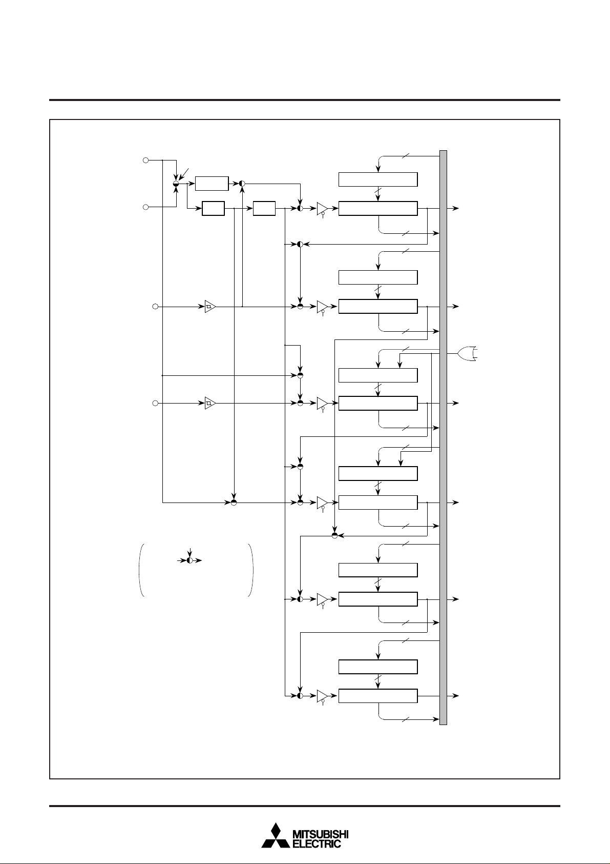
X
CIN
XIN
TIM2
MITSUBISHI MICROCOMPUTERS
M37272M6/M8–XXXSP/FP, M37272MA–XXXSP
M37272E8SP/FP, M37272EFSP
SINGLE-CHIP 8-BIT CMOS MICROCOMPUTER with CLOSED CAPTION DECODER
and ON-SCREEN DISPLAY CONTROLLER
Data bus
8
CM7
1/4096
1/2
TM15
1/8
TM10
TM12
TM14
TM11
TM13
Timer 1 latch (8)
8
Timer 1 (8)
Timer 2 latch (8)
8
Timer 2 (8)
Timer 1
interrupt request
8
8
Timer 2
interrupt request
8
TIM3
Selection gate: Connected to
black side at
reset
TM1 : Timer mode register 1
TM2 : Timer mode register 2
T3SC : Timer 3 count source
switch bit (address 00C7
CM : CPU mode register
TM21
16)
TM20
TM24
TM27
T3SC
TM22
TM21
TM23
TM25
TM16
Timer 3 latch (8)
8
Timer 3 (8)
Timer 4 latch (8)
8
Timer 4 (8)
Timer 5 latch (8)
8
Timer 5 (8)
8
FF16
8
8
0716
8
8
8
8
Reset
STP instruction
Timer 3
interrupt request
Timer 4
interrupt request
Timer 5
interrupt request
Notes 1: HIGH pulse width of external clock inputs TIM2 and TIM3 needs 4 machine cycles or more.
2: When the external clock source is selected, timers 1, 2, and 3 are counted at a rising edge of input signal.
3: In the stop mode or the wait mode, external clock inputs TIM2 and TIM3 cannot be used.
Fig. 8.4.3 Timer Block Diagram
Rev. 1.3
TM17
TM26
Timer 6 latch (8)
8
Timer 6 (8)
Timer 6
interrupt request
8
25
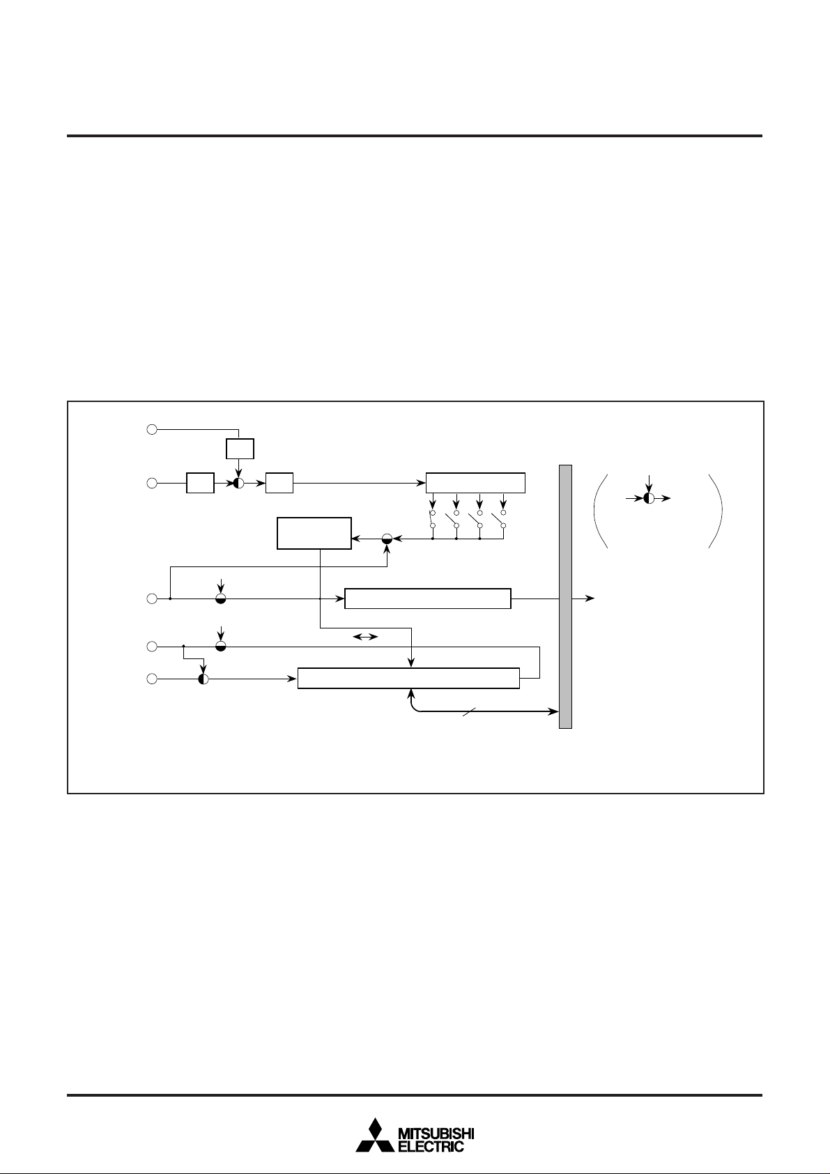
MITSUBISHI MICROCOMPUTERS
M37272M6/M8–XXXSP/FP, M37272MA–XXXSP
M37272E8SP/FP, M37272EFSP
SINGLE-CHIP 8-BIT CMOS MICROCOMPUTER with CLOSED CAPTION DECODER
and ON-SCREEN DISPLAY CONTROLLER
8.5 SERIAL I/O
This microcomputer has a built-in serial I/O which can either transmit
or receive 8-bit data serially in the clock synchronous mode.
The serial I/O block diagram is shown in Figure 8.5.1. The synchronous clock I/O pin (SCLK), and data output pin (SOUT) also function
as port P4, data input pin (SIN) also functions as port P20–P22.
Bit 3 of the serial I/O mode register (address 00EB16) selects whether
the synchronous clock is supplied internally or externally (from the
SCLK pin). When an internal clock is selected, bits 1 and 0 select
whether f(XIN) or f(XCIN) is divided by 8, 16, 32, or 64. T o use the S IN
pin for serial I/O, set the corresponding bit of the port P2 direction
register (address 00C516) to “0.”
X
CIN
1/2
X
IN
1/2
P20 Latch
S
CLK
SM3
P21 Latch
S
OUT
S
IN
SM3
SM6
CM7
1/2
Synchronous
SM5
circuit
Serial I/O counter (8)
: LSB
Serial I/O shift register (8)
SM2
S
MSB
The operation of the serial I/O is described below. The operation of
the serial I/O differs depending on the clock source; external clock or
internal clock.
Data bus
Frequency divider
1/2
1/81/4 1/16
SM1
SM0
Selection gate: Connect to
black side at
reset.
CM : CPU mode register
SM : Serial I/O mode register
Serial I/O
interrupt request
(See note)
8
Note : When the data is set in the serial I/O register (address 00EA
Fig. 8.5.1 Serial I/O Block Diagram
26
16
), the register functions as the serial I/O shift register.
Rev. 1.3
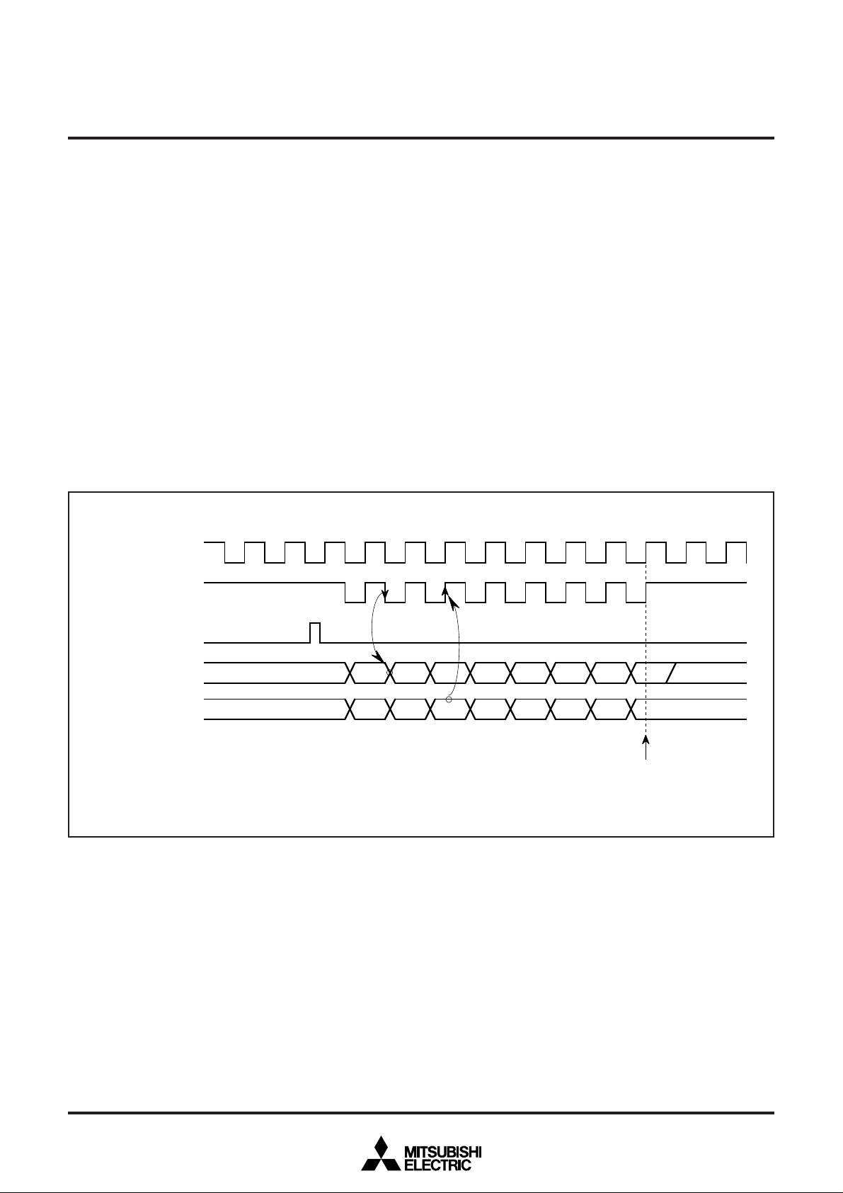
MITSUBISHI MICROCOMPUTERS
k
M37272M6/M8–XXXSP/FP, M37272MA–XXXSP
M37272E8SP/FP, M37272EFSP
SINGLE-CHIP 8-BIT CMOS MICROCOMPUTER with CLOSED CAPTION DECODER
and ON-SCREEN DISPLAY CONTROLLER
Internal clock : The serial I/O counter is set to “7” during the write
cycle into the serial I/O register (address 00EA16), and the transfer
clock goes HIGH forcibly. At each falling edge of the transfer clock
after the write cycle, serial data is output from the SOUT pin. Transfer
direction can be selected by bit 5 of the serial I/O mode register. At
each rising edge of the transfer clock, data is input from the SIN pin
and data in the serial I/O register is shifted 1 bit.
After the transfer clock has counted 8 times, the serial I/O counter
becomes “0” and the transfer clock stops at HIGH. At this time the
interrupt request bit is set to “1.”
S y n c h r o n o u s c l o c
External clock : The an external clock is selected as the clock source,
the interrupt request is set to “1” after the transfer clock has been
counted 8 counts. However, transfer operation does not stop, so the
clock should be controlled externally. Use the external clock of 1 MHz
or less with a duty cycle of 50%.
The serial I/O timing is shown in Figure 8.5.2. When using an external clock for transfer, the external clock must be held at HIGH for
initializing the serial I/O counter. When switching between an internal clock and an external clock, do not switch during transfer. Also,
be sure to initialize the serial I/O counter after switching.
Notes 1: On programming, note that the serial I/O counter is set by writing to
the serial I/O register with the bit managing instructions, such as SEB
and CLB.
2:When an external clock is used as the synchronous clock, write trans-
mit data to the serial I/O register when the transfer clock input level is
HIGH.
T r a n s f e r c l o c k
S e r i a l I / O r e g i s t e r
w r i t e s i g n a l
S e r i a l I / O o u t p u t
S
O U T
S e r i a l I / O i n p u t
S
I N
N o t e : W h e n a n i n t e r n a l c l o c k i s s e l e c t e d , t h e S
Fig. 8.5.2 Serial I/O Timing (for LSB first)
D
0
D
1
D
2
D
3
D
4
D
O U T
p i n i s a t h i g h - i m p e d a n c e a f t e r t r a n s f e r i s c o m p l e t e d .
( N o t e )
5
D
6
D
7
I n t e r r u p t r e q u e s t b i t i s s e t t o “ 1 ”
Rev. 1.3
27
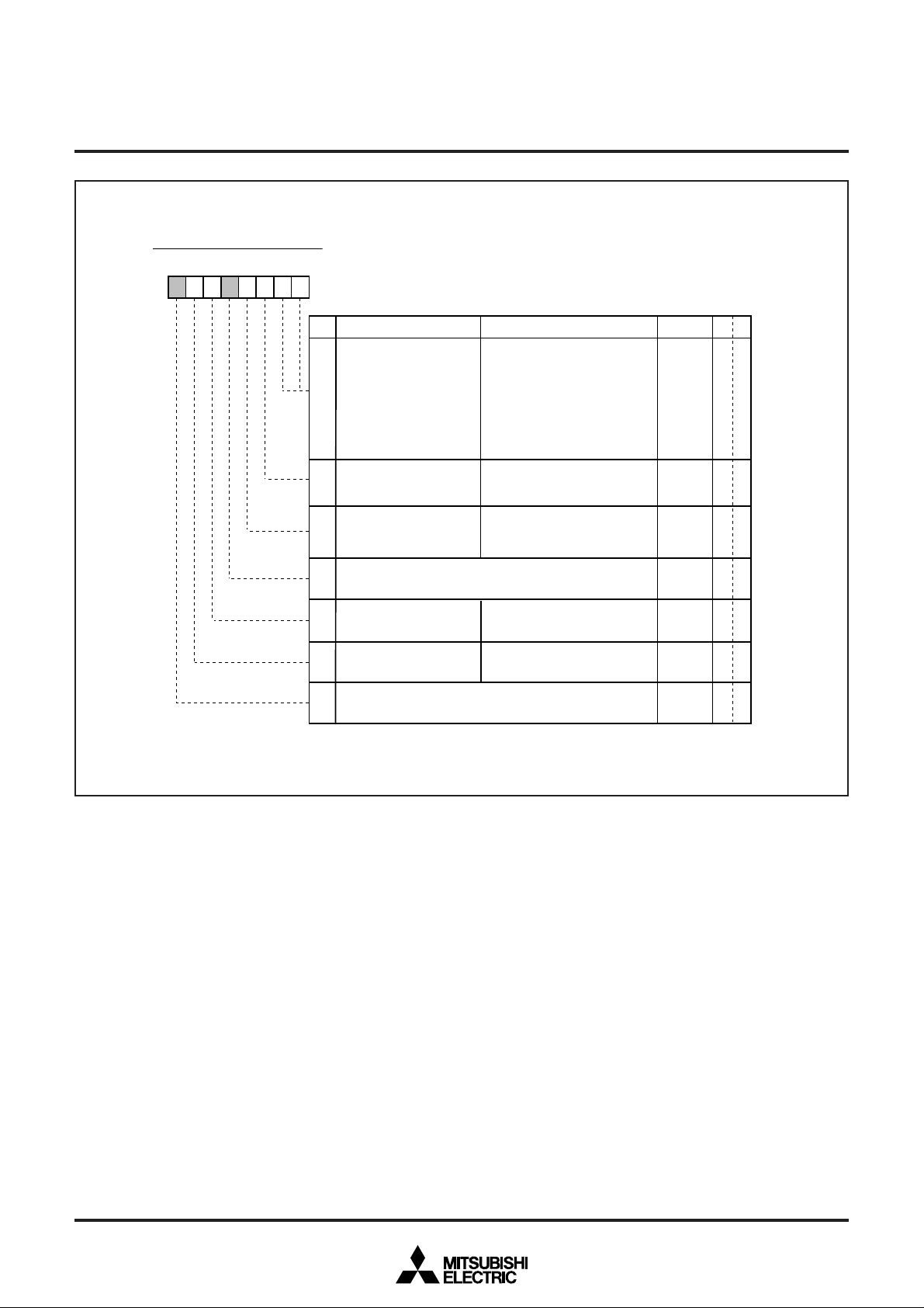
r
0
W
W
S e r i a l I / O M o d e R e g i s t e
b 7b 6 b 5b 4b 3 b 2b 1b 0
0
MITSUBISHI MICROCOMPUTERS
M37272M6/M8–XXXSP/FP, M37272MA–XXXSP
M37272E8SP/FP, M37272EFSP
SINGLE-CHIP 8-BIT CMOS MICROCOMPUTER with CLOSED CAPTION DECODER
and ON-SCREEN DISPLAY CONTROLLER
1 6
S e r i a l I / O m o d e r e g i s t e r ( S M ) [ A d d r e s s 0 0 E B
]
BN
0 , 1
a m
eF
I n t e r n a l s y n c h r o n o u s
c l o c k s e l e c t i o n b i t s
( S M 0 , S M 1 )
2
S y n c h r o n o u s c l o c k
s e l e c t i o n b i t ( S M 2 )
3
P o r t f u n c t i o n
s e l e c t i o n b i t ( S M 3 )
F i x t h i s b i t t o “ 0 . ”
4
T r a n s f e r d i r e c t i o n
5
s e l e c t i o n b i t ( S M 5 )
6
T r a n s f e r c l o c k i n p u t
p i n s e l e c t i o n b i t ( S M 6 )
F i x t h i s b i t t o “ 0 . ”
7
u n c t i o n
s
b 1 b 0
0 0 : f ( X
0 1 : f ( X
1 0 : f ( X
1 1 : f ( X
I N
) / 4 o r f ( X
I N
) / 1 6 o r f ( X
I N
) / 3 2 o r f ( X
I N
) / 6 4 o r f ( X
C I N
0 : E x t e r n a l c l o c k
1 : I n t e r n a l c l o c k
0 : P 20, P 2
1 : S
C L K
, S
1
O U T
0 : L S B f i r s t
1 : M S B f i r s t
0 : I n p u t s i g n a l f r o m S
1 :
I n p u t s i g n a l f r o m S
C I N
C I N
C I N
O U T
) / 4
) / 1 6
) / 3 2
) / 6 4
I N
p i n
p i n
A f t e r r e s e t
0
0
0
0
0
0
0R
RW
RW
RW
RW
R
RW
RW
Fig. 8.5.3 Serial I/O Mode Register
Rev. 1.3
28
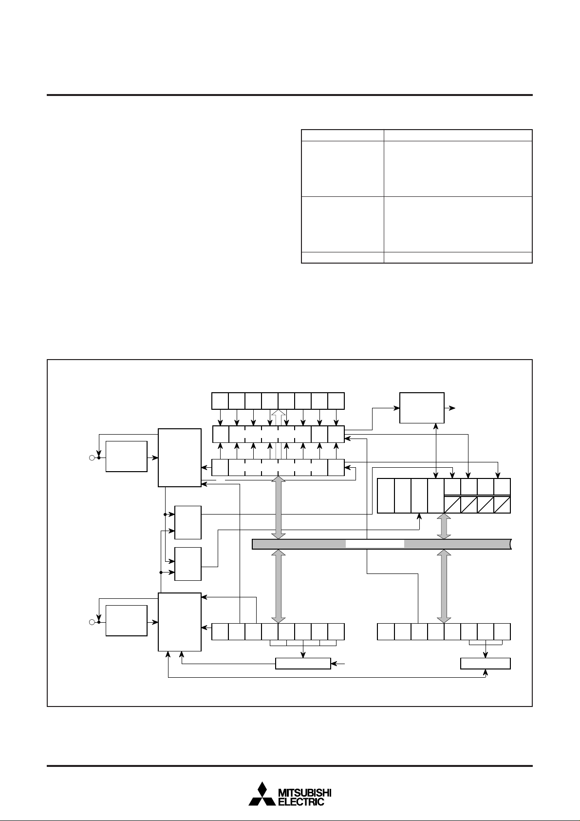
MITSUBISHI MICROCOMPUTERS
BSEL1
BSEL0
M37272M6/M8–XXXSP/FP, M37272MA–XXXSP
M37272E8SP/FP, M37272EFSP
SINGLE-CHIP 8-BIT CMOS MICROCOMPUTER with CLOSED CAPTION DECODER
and ON-SCREEN DISPLAY CONTROLLER
8.6 MULTI-MASTER I2C-BUS INTERFACE
The multi-master I2C-BUS interface is a serial communications circuit, conforming to the Philips I2C-BUS data transfer format. This
interface, offering both arbitration lost detection and a synchronous
functions, is useful for the multi-master serial communications.
Figure 8.6.1 shows a block diagram of the multi-master I2C-BUS interface and Table 8.6.1 shows multi-master I2C-BUS interface functions.
This multi-master I2C-BUS interface consists of the I2C address register, the I2C data shift register, the I2C clock control register, the I2C
control register, the I2C status register and other control circuits.
I2C address register (S0D)
b7 b0
SAD6 SAD5 SAD4 SAD3 SAD2 SAD1SAD0 RBW
Table 8.6.1 Multi-master I2C-BUS Interface Functions
Item
Function
In conformity with Philips I2C-BUS
standard:
10-bit addressing format
Format
7-bit addressing format
High-speed clock mode
Standard clock mode
In conformity with Philips I2C-BUS
standard:
Master transmission
Communication mode
Master reception
Slave transmission
Slave reception
SCL clock frequency
16.1 kHz to 400 kHz (at φ = 4 MHz)
φ : System clock = f(XIN)/2
Note :W e are not responsible for any third party’s infringement of patent rights
or other rights attributable to the use of the control function (bits 6 and 7
2
of the I
C control register at address 00F916) for connections between
2
the I
C-BUS interface and ports (SCL1, SCL2, SDA1, SDA2).
Interrupt
generating
circuit
Interrupt
request signal
(IICIRQ)
Serial
data
(SDA)
Serial
clock
(SCL)
Noise
elimination
circuit
Noise
elimination
circuit
Data
control
circuit
AL
circuit
BB
circuit
Clock
control
circuit
Address comparator
b7
2
I C data shift register
S0
b7 b0
FAST
ACK
ACK
BIT
I2C clock control register (S2)
CCR4 CCR3 CCR2 CCR1 CCR0
MODE
Clock division
b0
Internal data bus
System clock
b7
MST TRX BB PIN
AL AAS AD0 LRB
2
I C status
register
(S1)
b7 b0
10BIT
ALS
SAD
I2C control register (S1D)
(φ)
BC2 BC1 BC0
ESO
Bit counter
b0
Fig. 8.6.1 Block Diagram of Multi-master I2C-BUS Interface
Rev. 1.3
29
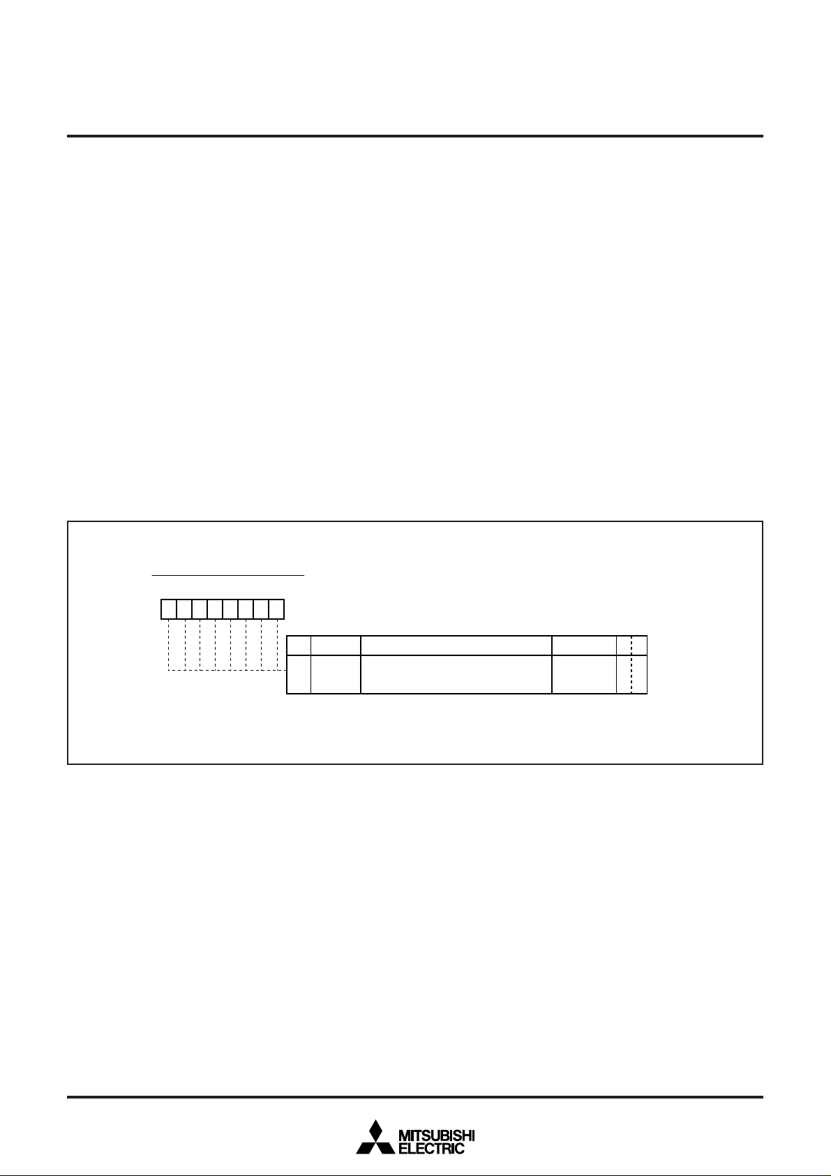
M37272M6/M8–XXXSP/FP, M37272MA–XXXSP
C
B
s
f
C
f
C
e
SINGLE-CHIP 8-BIT CMOS MICROCOMPUTER with CLOSED CAPTION DECODER
8.6.1 I2C Data Shift Register
The I2C data shift register (S0 : address 00F616) is an 8-bit shift
register to store receive data and write transmit data.
When transmit data is written into this register, it is transferred to the
outside from bit 7 in synchronization with the SCL clock, and each
time one-bit data is output, the data of this register are shifted one bit
to the left. When data is received, it is input to this register from bit 0
in synchronization with the SCL clock, and each time one-bit data is
input, the data of this register are shifted one bit to the left.
The I2C data shift register is in a write enable status only when the
ESO bit of the I2C control register (address 00F916) is “1.” The bit
counter is reset by a write instruction to the I2C data shift register.
When both the ESO bit and the MST bit of the I2C status register
(address 00F816) are “1,” the SCL is output by a write instruction to
the I2C data shift register. Reading data from the I2C data shift register is always enabled regardless of the ESO bit value.
MITSUBISHI MICROCOMPUTERS
M37272E8SP/FP, M37272EFSP
and ON-SCREEN DISPLAY CONTROLLER
Note: To write data into the I2C data shift register after setting the MST bit to
“0” (slave mode), keep an interval of 8 machine cycles or more.
D a t a S h i f t R e g i s t e
2
I
b 7b 6b 5b 4b 3b 2b 1b 0
r
d a t a s h i f t r e g i s t e r 1 ( S 0 ) [ A d d r e s s 0 0 F
2
I
N a m
0
D 0 t o D 7RW
t o
7
d a t a s h i f t r e g i s t e r a f t e r s e t t i n g t h e M S T b i t t
N o t e :
T o w r i t e d a t a i n t o t h e I
“ 0 ” ( s l a v e m o d e ) , k e e p a n i n t e r v a l o f 8 m a c h i n e c y c l e s o r m o r e .
t r e g i s t e r t o s t o r e
T h i s i s a n 8 - b i t s h i
r e c e i v e d a t a a n d w r i t e t r a n s m i t d a t a .
Fig. 8.6.2 Data Shift Register
2
F u n c t i o n
1 6
]
6
t e r r e s e
I n d e t e r m i n a t e
A
tRW
o
Rev. 1.3
30

M37272M6/M8–XXXSP/FP, M37272MA–XXXSP
/
S
O
B
e
s
W
W
SINGLE-CHIP 8-BIT CMOS MICROCOMPUTER with CLOSED CAPTION DECODER
8.6.2 I2C Address Register
The I2C address register (address 00F716) consists of a 7-bit slave
address and a read/write bit. In the addressing mode, the slave address written in this register is compared with the address data to be
received immediately after the START condition are detected.
(1) Bit 0: read/write bit (RBW)
Not used when comparing addresses, in the 7-bit addressing mode.
In the 10-bit addressing mode, the first address data to be received
is compared with the contents (SAD6 to SAD0 + RBW) of the I2C
address register.
The RBW bit is cleared to “0” automatically when the stop condition
is detected.
(2) Bits 1 to 7: slave address (SAD0–SAD6)
These bits store slave addresses. Regardless of the 7-bit addressing mode and the 10-bit addressing mode, the address data transmitted from the master is compared with the contents of these bits.
MITSUBISHI MICROCOMPUTERS
M37272E8SP/FP, M37272EFSP
and ON-SCREEN DISPLAY CONTROLLER
I2C A d d r e s s R e g i s t e r
b 7b 6b 5b 4b 3b 2b 1b 0
Fig. 8.6.3 I2C Address Register
I2C a d d r e s s r e g i s t e r ( S 0 D ) [ A d d r e s s 0 0 F 7
w r i t e b i
0R e a d
( R B W )
l a v e a d d r e s
1
( S A D 0 t o S A D 6 )
t o
7
N a m
n l y i n 1 0 - b i t a d d r e s s i n g ( i n s l a v e ) m o d e
<
t
T h e l a s t s i g n i f i c a n t b i t o f a d d r e s s d a t a i s
c o m p a r e d .
0 : W a i t t h e f i r s t b y t e o f s l a v e a d d r e s s a f t e r
S T A R T c o n d i t i o n
1 : W a i t t h e f i r s t b y t e o f s l a v e a d d r e s s a f t e r
R E S T A R T c o n d i t i o n
s
< I n b o t h m o d e s >
T h e a d d r e s s d a t a i s c o m p a r e d .
F u n c t i o n
( r e a d s t a t e )
( w r i t e s t a t e )
1 6
]
A f t e r r e s e t
>
R
0
R—
0
R
Rev. 1.3
31

MITSUBISHI MICROCOMPUTERS
M37272M6/M8–XXXSP/FP, M37272MA–XXXSP
M37272E8SP/FP, M37272EFSP
SINGLE-CHIP 8-BIT CMOS MICROCOMPUTER with CLOSED CAPTION DECODER
and ON-SCREEN DISPLAY CONTROLLER
8.6.3 I2C Clock Control Register
The I2C clock control register (address 00FA16) is used to set ACK
control, SCL mode and SCL frequency.
(4) Bit 7: ACK clock bit (ACK)
This bit specifies a mode of acknowledgment which is an acknowledgment response of data transmission. When this bit is set to “0,”
the no ACK clock mode is set. In this case, no ACK clock occurs
(1) Bits 0 to 4: SCL frequency control bits (CCR0–CCR4)
These bits control the SCL frequency.
after data transmission. When the bit is set to “1,” the ACK clock
mode is set and the master generates an ACK clock upon completion of each 1-byte data transmission.The device for transmitting
(2) Bit 5: SCL mode specification bit (FAST MODE)
This bit specifies the SCL mode. When this bit is set to “0,” the standard clock mode is set. When the bit is set to “1,” the high-speed
address data and control data releases the SDA at the occurrence of
an ACK clock (make SDA HIGH) and receives the ACK bit generated
by the data receiving device.
clock mode is set.
Note: Do not write data into the I2C clock control register during transmission.
(3) Bit 6: ACK bit (ACK BIT)
This bit sets the SDA status when an ACK clock✽ is generated. When
this bit is set to “0,” the ACK return mode is set and SDA goes to
LOW at the occurrence of an ACK clock. When the bit is set to “1,”
the ACK non-return mode is set. The SDA is held in the HIGH status
at the occurrence of an ACK clock.
However, when the slave address matches the address data in the
reception of address data at ACK BIT = “0,” the SDA is automatically
made LOW (ACK is returned). If there is a mismatch between the
slave address and the address data, the SDA is automatically made
HIGH (ACK is not returned).
✽ACK clock: Clock for acknowledgement
If data is written during transmission, the I
that data cannot be transmitted normally.
2
C clock generator is reset, so
I2C Clock Control Register
b7 b6 b5 b4 b3 b2 b1 b0
2
I
C clock control register (S2 : address 00FA16)
B Name Functions
0
SCL frequency control
to
bits
4
(CCR0 to CCR4)
56SCL mode
specification bit
(FAST MODE)
ACK bit
(ACK BIT)
ACK clock bit
7
(ACK)
Note: At 4000kHz in the high-speed clock mode, the duty is as below .
“0” period : “1” period = 3 : 2
In the other cases, the duty is as below.
“0” period : “1” period = 1 : 1
Setup value
of CCR4–
CCR0
00 to 02
05
...
1D
1E
1F
0: Standard clock mode
1: High-speed clock mode
0: ACK is returned.
1: ACK is not returned.
0: No ACK clock
1: ACK clock
mode
Setup disabled Setup disabled
Setup disabled
Setup disabled
100
83.3 16606
500/CCR value 1000/CCR value
17.2 34.5
16.6 33.3
16.1
(at
φ
= 4 MHz, unit : kHz)
Standard clock
High speed
clock mode
33303
25004
400 (See note)
32.3
After reset
0
0
0
0
RW
RW
RW
RW
RW
Fig. 8.6.4 I2C Address Register
32
Rev. 1.3

MITSUBISHI MICROCOMPUTERS
M37272M6/M8–XXXSP/FP, M37272MA–XXXSP
M37272E8SP/FP, M37272EFSP
SINGLE-CHIP 8-BIT CMOS MICROCOMPUTER with CLOSED CAPTION DECODER
and ON-SCREEN DISPLAY CONTROLLER
8.6.4 I2C Control Register
The I2C control register (address 00F916) controls the data communication format.
(1) Bits 0 to 2: bit counter (BC0–BC2)
These bits decide the number of bits for the next 1-byte data to be
transmitted. An interrupt request signal occurs immediately after the
number of bits specified with these bits are transmitted.
When a STAR T condition is received, these bits become “0002” and
the address data is always transmitted and received in 8 bits.
(2) Bit 3: I2C interface use enable bit (ESO)
This bit enables usage of the multimaster I2C BUS interface. When
this bit is set to “0,” the use disable status is provided, so the SDA
and the SCL become high-impedance. When the bit is set to “1,” use
of the interface is enabled.
When ESO = “0,” the following is performed.
• PIN = “1,” BB = “0” and AL = “0” are set (they are bits of the I2C
status register at address 00F816 ).
• Writing data to the I2C data shift register (address 00F616) is disabled.
S C L
M u l t i - m a s t e r
I2C - B U S
i n t e r f a c e
S D A
(3) Bit 4: data format selection bit (ALS)
This bit decides whether or not to recognize slave addresses. When
this bit is set to “0,” the addressing format is selected, so that address data is recognized. When a match is found between a slave
address and address data as a result of comparison or when a general call (refer to “8.6.5 I2C Status Register,” bit 1) is received, transmission processing can be performed. When this bit is set to “1,” the
free data format is selected, so that slave addresses are not recognized.
(4) Bit 5: addressing format selection bit (10BIT SAD)
This bit selects a slave address specification format. When this bit is
set to “0,” the 7-bit addressing format is selected. In this case, only
the high-order 7 bits (slave address) of the I2C address register (address 00F716) are compared with address data. When this bit is set
to “1,” the 10-bit addressing format is selected, all the bits of the I2C
address register are compared with address data.
(5) Bits 6 and 7: connection control bits between
2
C-BUS interface and ports
I
(BSEL0, BSEL1)
These bits controls the connection between SCL and ports or SDA
and ports (refer to Figure 8.6.5).
“ 0 ”
“ 1 ” B S E L 0
S C L / P 1
S C L 2 / P 1
S D A 1 / P 1
S D A 2 / P 1
1
2
3
4
“ 0 ”
“ 1 ” B S E L 1
“ 0 ”
“ 1 ” B S E L 0
“ 0 ”
“ 1 ” B S E L 1
Note: Set the corresponding direction register to “1” to use the
port as multi-master I2C-BUS interface.
Fig. 8.6.5 Connection Port Control by BSEL0 and BSEL1
Rev. 1.3
33

f
f
7
C
C
)
I2C C o n t r o l R e g i s t e r
B
e
s
W
C
WRWRWRWRW
MITSUBISHI MICROCOMPUTERS
M37272M6/M8–XXXSP/FP, M37272MA–XXXSP
M37272E8SP/FP, M37272EFSP
SINGLE-CHIP 8-BIT CMOS MICROCOMPUTER with CLOSED CAPTION DECODER
and ON-SCREEN DISPLAY CONTROLLER
b 7b 6b 5b 4b 3b 2b 1b 0
2
C c o n t r o l r e g i s t e r ( S 1 D a d d r e s s 0 0 F 91
I
N a m
B i t c o u n t e r
0
( N u m b e r o f t r a n s m i t / r e c i e v e
t o
b i t s )
2
( B C 0 t o B C 2 )
2
3
C - B U S i n t e r f a c e u s e
I
e n a b l e b i t ( E S O )
o r m a t s e l e c t i o n
4D a t a
b i t ( A L S )
o r m a t s e l e c t i o n
5A d d r e s s i n g
b i t ( 1 0 B I T S A D )
o n n e c t i o n c o n t r o l b i t s
6 ,
- B U S i n t e r f a c e , t h e o u t p u t s t r u c t u r e c h a n g e s
N o t e : W h e n u s i n g p o r t s P 11- P 14 a s I
2
b e t w e e n I C - B U S i n t e r f a c e
a n d p o r t s
a u t o m a t i c a l l y f r o m C M O S o u t p u t t o N - c h a n n e l o p e n - d r a i n o u t p u t .
6)
F u n c t i o n
b 2 b 1 b 0
0 0 0 : 8
0 0 1 : 7
0 1 0 : 6
0 1 1 : 5
1 0 0 : 4
1 0 1 : 3
1 1 0 : 2
1 1 1 : 1
0 : D i s a b l e d
1 : E n a b l e d
0 : A d d r e s s i n g m o d e
1 : F r e e d a t a f o r m a t
0 : 7 - b i t a d d r e s s i n g f o r m a t
1 : 1 0 - b i t a d d r e s s i n g f o r m a t
o n n e c t i o n p o r t ( S e e n o t e
b 7 b 6
0 0 : N o n e
0 1 : S C L 1 , S D A 1
1 0 : S C L 2 , S D A 2
1 1 : S C L 1 , S D A 1
S C L 2 , S D A 2
2
A f t e r r e s e t
0
0
0
0
0
R
R
Fig. 8.6.6 I2C Control Register
Rev. 1.3
34

MITSUBISHI MICROCOMPUTERS
M37272M6/M8–XXXSP/FP, M37272MA–XXXSP
M37272E8SP/FP, M37272EFSP
SINGLE-CHIP 8-BIT CMOS MICROCOMPUTER with CLOSED CAPTION DECODER
and ON-SCREEN DISPLAY CONTROLLER
8.6.5 I2C Status Register
The I2C status register (address 00F816) controls the I2C-BUS interface status. The low-order 4 bits are read-only bits and the highorder 4 bits can be read out and written to.
(1) Bit 0: last receive bit (LRB)
This bit stores the last bit value of received data and can also be
used for ACK receive confirmation. If ACK is returned when an ACK
clock occurs, the LRB bit is set to “0.” If ACK is not returned, this bit is
set to “1.” Except in the ACK mode, the last bit value of received data
is input. The state of this bit is changed from “1” to “0” by executing a
write instruction to the I2C data shift register (address 00F616).
(2) Bit 1: general call detecting flag (AD0)
This bit is set to “1” when a general call✽ whose address data is all
“0” is received in the slave mode. By a general call of the master
device, every slave device receives control data after the general
call. The AD0 bit is set to “0” by detecting the STOP condition or
START condition.
✽General call: The master transmits the general call address “0016”
to all slaves.
(3) Bit 2: slave address comparison flag (AAS)
This flag indicates a comparison result of address data.
■ In the slave receive mode, when the 7-bit addressing format is
selected, this bit is set to “1” in one of the following conditions.
• The address data immediately after occurrence of a ST ART con-
dition matches the slave address stored in the high-order 7 bits
of the I2C address register (address 00F716).
• A general call is received.
■ In the slave reception mode, when the 10-bit addressing format is
selected, this bit is set to “1” with the following condition.
• When the address data is compared with the I2C address regis-
ter (8 bits consists of slave address and RBW), the first bytes
match.
■ The state of this bit is changed from “1” to “0” by executing a write
instruction to the I2C data shift register (address 00F616).
(4) Bit 3: arbitration lost✽ detecting flag (AL)
n the master transmission mode, when a device other than the microcomputer sets the SDA to “L,”, arbitration is judged to have been
lost, so that this bit is set to “1.” At the same time, the TRX bit is set to
“0,” so that immediately after transmission of the byte whose arbitration was lost is completed, the MST bit is set to “0.” When arbitration
is lost during slave address transmission, the TRX bit is set to “0” and
the reception mode is set. Consequently, it becomes possible to receive and recognize its own slave address transmitted by another
master device.
✽Arbitration lost: The status in which communication as a master is
disabled.
(5) Bit 4: I2C-BUS interface interrupt request bit (PIN)
This bit generates an interrupt request signal. Each time 1-byte data
is transmitted, the state of the PIN bit changes from “1” to “0.” At the
same time, an interrupt request signal is sent to the CPU. The PIN bit
is set to “0” in synchronization with a falling edge of the last clock
(including the ACK clock) of an internal clock and an interrupt request signal occurs in synchronization with a falling edge of the PIN
bit. When the PIN bit is “0,” the SCL is kept in the “0” state and clock
generation is disabled. Figure 8.6.8 shows an interrupt request signal generating timing chart.
The PIN bit is set to “1” in any one of the following conditions.
• Executing a write instruction to the I2C data shift register (address
00F616).
• When the ESO bit is “0”
• At reset
The conditions in which the PIN bit is set to “0” are shown below:
• Immediately after completion of 1-byte data transmission (including when arbitration lost is detected)
• Immediately after completion of 1-byte data reception
• In the slave reception mode, with ALS = “0” and immediately after
completion of slave address or general call address reception
• In the slave reception mode, with ALS = “1” and immediately after
completion of address data reception
(6) Bit 5: bus busy flag (BB)
This bit indicates the status of use of the bus system. When this bit is
set to “0,” this bus system is not busy and a ST ART condition can be
generated. When this bit is set to “1,” this bus system is busy and the
occurrence of a STAR T condition is disabled by the ST AR T condition
duplication prevention function (See note).
This flag can be written by software only in the master transmission
mode. In the other modes, this bit is set to “1” by detecting a STAR T
condition and set to “0” by detecting a STOP condition. When the
ESO bit of the I2C control register (address 00F916) is “0” and at
reset, the BB flag is kept in the “0” state.
(7) Bit 6: communication mode specification bit
(transfer direction specification bit: TRX)
This bit decides the direction of transfer for data communication. When
this bit is “0,” the reception mode is selected and the data of a transmitting device is received. When the bit is “1,” the transmission mode
is selected and address data and control data are output into the
SDA in synchronization with the clock generated on the SCL.
When the ALS bit of the I2C control register (address 00F916) is “0” in
the slave reception mode is selected, the TRX bit is set to “1” (transmit) if the least significant bit (R/W bit) of the address data transmitted by the master is “1.” When the ALS bit is “0” and the R/W bit is
“0,” the TRX bit is cleared to “0” (receive).
The TRX bit is cleared to “0” in one of the following conditions.
• When arbitration lost is detected.
• When a STOP condition is detected.
• When occurence of a START condition is disabled by the START
condition duplication prevention function (Note).
• With MST = “0” and when a START condition is detected.
• With MST = “0” and when ACK non-return is detected.
• At reset
Rev. 1.3
35

MITSUBISHI MICROCOMPUTERS
7
B
e
s
W
C
f
)
f
S
G
“
)
W
W
( S
)
( S
)
( S
)
( S
)
Q
M37272M6/M8–XXXSP/FP, M37272MA–XXXSP
M37272E8SP/FP, M37272EFSP
SINGLE-CHIP 8-BIT CMOS MICROCOMPUTER with CLOSED CAPTION DECODER
and ON-SCREEN DISPLAY CONTROLLER
(8) Bit 7: Communication mode specification bit
(master/slave specification bit: MST)
This bit is used for master/slave specification for data communication. When this bit is “0,” the slave is specified, so that a START
condition and a STOP condition generated by the master are received,
and data communication is performed in synchronization with the
clock generated by the master. When this bit is “1,” the master is
specified and a START condition and a STOP condition are generated, and also the clocks required for data communication are generated on the SCL.
The MST bit is cleared to “0” in one of the following conditions.
• Immediately after completion of 1-byte data transmission when
arbitration lost is detected
• When a STOP condition is detected.
• When occurence of a START condition is disabled by the START
condition duplication preventing function (Note).
• At reset
I2C S t a t u s R e g i s t e r
b 7b 6b 5b 4b 3b 2b 1b 0
I2C s t a t u s r e g i s t e r ( S 1 ) [ A d d r e s s 0 0 F 8
N a m
( L R B
0
L a s t r e c e i v e b i t
( S e e n o t e )
e n e r a l c a l l d e t e c t i n g f l a g
1
( A D 0 ) ( S e e n o t e )
l a v e a d d r e s s c o m p a r i s o n
2
f l a g ( A A S ) ( S e e n o t e )
l a g
3
A r b i t r a t i o n l o s t d e t e c t i n g
( A L ) ( S e e n o t e )
2
4
C - B U S i n t e r f a c e i n t e r r u p t
I
r e q u e s t b i t ( P I N )
f l a g ( B B
5
B u s b u s y
o m m u n i c a t i o n m o d e
6 ,
s p e c i f i c a t i o n b i t s
( T R X , M S T )
f l a g s c a n b e r e a d o u t , b u t c a n n n o t b e w r i t t e n
N o t e : T h e s e b i t s a n d
Note:The START condition duplication prevention function disables the ST ART
condition generation, reset of bit counter reset, and SCL output, when
the following condition is satisfied:
a START condition is set by another master device.
1 6
]
0
0 : L a s t b i t =
1 : L a s t b i t = “ 1 ”
0 : N o g e n e r a l c a l l d e t e c t e d
1 : G e n e r a l c a l l d e t e c t e d
0 : A d d r e s s m i s m a t c h
1 : A d d r e s s m a t c h
0 : N o t d e t e c t e d
1 : D e t e c t e d
0 : I n t e r r u p t r e q u e s t i s s u e d
1 : N o i n t e r r u p t r e q u e s t i s s u e d
r e
0 : B u s
1 : B u s b u s y
b 7 b 6
0 0 : S l a v e r e c i e v e m o d e
0 1 : S l a v e t r a n s m i t m o d e
1 0 : M a s t e r r e c i e v e m o d e
1 1 : M a s t e r t r a n s m i t m o d e
F u n c t i o n
”
e
e e n o t e
e e n o t e
e e n o t e
e e n o t e
.
A f t e r r e s e t
I n d e t e r m i n a t e
0
0
0
1
0
0
R
R—
R—
R—
R—
RW
R
R
Fig. 8.6.7 I2C Status Register
S C L
P I N
I I C I R
Fig. 8.6.8 Interrupt Request Signal Generation Timing
Rev. 1.3
36

M37272M6/M8–XXXSP/FP, M37272MA–XXXSP
S
SINGLE-CHIP 8-BIT CMOS MICROCOMPUTER with CLOSED CAPTION DECODER
8.6.6 START Condition Generation Method
When the ESO bit of the I2C control register (address 00F916) is “1,”
execute a write instruction to the I2C status register (address 00F816)
to set the MST, TRX and BB bits to “1.” A ST ART condition will then
be generated. After that, the bit counter becomes “0002” and an SCL
for 1 byte is output. The START condition generation timing and BB
bit set timing are different in the standard clock mode and the highspeed clock mode. Refer to Figure 8.6.9 for the START condition
generation timing diagram, and T able 8.6.2 for the START condition/
STOP condition generation timing table.
8.6.7 STOP Condition Generation Method
When the ESO bit of the I2C control register (address 00F916) is “1,”
execute a write instruction to the I2C status register (address 00F816)
for setting the MST bit and the TRX bit to “1” and the BB bit to “0”. A
STOP condition will then be generated. The STOP condition generation timing and the BB flag reset timing are different in the standard
clock mode and the high-speed clock mode. Refer to Figure 8.6.10
for the STOP condition generation timing diagram, and Table 8.6.2
for the START condition/STOP condition generation timing table.
MITSUBISHI MICROCOMPUTERS
M37272E8SP/FP, M37272EFSP
and ON-SCREEN DISPLAY CONTROLLER
2
I
C s t a t u s r e g i s t e r
w r i t e s i g n a l
S C L
S D A
B B f l a g
Fig. 8.6.9 START Condition Generation Timing Diagram
I2C s t a t u s r e g i s t e r
w r i t e s i g n a l
S C L
S D A
B B f l a g
S e t u p
t i m e
S e t u p
t i m e
H o l d t i m e
e t t i m e
f o r B B f l a g
H o l d t i m e
R e se t t i m e
f o r B B f l a g
Fig. 8.6.10 STOP Condition Generation Timing Diagram
Table 8.6.2 START Condition/STOP Condition Generation Tim-
ing Table
Item
Setup time
(START condition)
Setup time
(STOP condition)
Hold time
Set/reset time
for BB flag
Note: Absolute time at φ = 4 MHz. The value in parentheses denotes the
number of φ cycles.
Standard Clock Mode
5.0 µs (20 cycles)
4.25 µs (17 cycles)
5.0 µs (20 cycles)
3.0 µs (12 cycles)
High-speed Clock Mode
2.5 µs (10 cycles)
1.75 µs (7 cycles)
2.5 µs (10 cycles)
1.5 µs (6 cycles)
Rev. 1.3
37

MITSUBISHI MICROCOMPUTERS
M37272M6/M8–XXXSP/FP, M37272MA–XXXSP
M37272E8SP/FP, M37272EFSP
SINGLE-CHIP 8-BIT CMOS MICROCOMPUTER with CLOSED CAPTION DECODER
and ON-SCREEN DISPLAY CONTROLLER
8.6.8 ST ART/STOP Condition Detect Conditions
The START/STOP condition detect conditions are shown in
Figure 8.6.11 and Table 8.6.3. Only when the 3 conditions of Table
8.6.3 are satisfied, a START/STOP condition can be detected.
Note: When a STOP condition is detected in the slave mode
(MST = 0), an interrupt request signal “IICIRQ” is generated to the
CPU.
S C L r e l e a s e t i m e
S C L
S D A
( S T A R T c o n d i t i o n )
S D A
( S T O P c o n d i t i o n )
Fig. 8.6.11 ST ART Condition/STOP Condition Detect Timing Dia-
gram
Table 8.6.3 ST ART Condition/ST OP Condition Detect Conditions
Standard Clock Mode
6.5 µs (26 cycles) < SCL
3.25 µs (13 cycles) < Setup time
3.25 µs (13 cycles) < Hold time
Note:Absolute time at φ = 4 MHz. The value in parentheses denotes the num-
ber of φ cycles.
release time
S e t u p
t i m e
S e t u p
t i m e
H o l d t i m e
H o l d t i m e
High-speed Clock Mode
1.0 µs (4 cycles) < SCL
0.5 µs (2 cycles) < Setup time
0.5 µs (2 cycles) < Hold time
release time
8.6.9 Address Data Communication
There are two address data communication formats, namely, 7-bit
addressing format and 10-bit addressing format. The respective address communication formats is described below.
(1) 7-bit addressing format
T o meet the 7-bit addressing format, set the 10BIT SAD bit of the I2C
control register (address 00F916) to “0.” The first 7-bit address data
transmitted from the master is compared with the high-order 7-bit
slave address stored in the I2C address register (address 00F716).
At the time of this comparison, address comparison of the RBW bit of
the I2C address register (address 00F716) is not made. For the data
transmission format when the 7-bit addressing format is selected,
refer to Figure 8.6.12, (1) and (2).
(2) 10-bit addressing format
To meet the 10-bit addressing format, set the 10BIT SAD bit of the
I2C control register (address 00F916) to “1.” An address comparison
is made between the first-byte address data transmitted from the
master and the 7-bit slave address stored in the I2C address register
(address 00F716). At the time of this comparison, an address comparison between the RBW bit of the I2C address register (address
00F716) and the R/W bit which is the last bit of the address data
transmitted from the master is made. In the 10-bit addressing mode,
the R/W bit which is the last bit of the address data not only specifies
the direction of communication for control data but also is processed
as an address data bit.
When the first-byte address data matches the slave address, the
AAS bit of the I2C status register (address 00F816) is set to “1.” After
the second-byte address data is stored into the I2C data shift register
(address 00F616), make an address comparison between the second-byte data and the slave address by software. When the address
data of the 2nd bytes matches the slave address, set the RBW bit of
the I2C address register (address 00F716) to “1” by software. This
processing can match the 7-bit slave address and R/W data, which
are received after a RESTART condition is detected, with the value
of the I2C address register (address 00F716). For the data transmission format when the 10-bit addressing format is selected, refer to
Figure 8.6.12, (3) and (4).
38
Rev. 1.3

MITSUBISHI MICROCOMPUTERS
M37272M6/M8–XXXSP/FP, M37272MA–XXXSP
M37272E8SP/FP, M37272EFSP
SINGLE-CHIP 8-BIT CMOS MICROCOMPUTER with CLOSED CAPTION DECODER
and ON-SCREEN DISPLAY CONTROLLER
8.6.10 Example of Master Transmission
An example of master transmission in the standard clock mode, at
the SCL frequency of 100 kHz and in the ACK return mode is shown
below.
➀ Set a slave address in the high-order 7 bits of the I2C address
register (address 00F716) and “0” in the RBW bit.
➁ Set the ACK return mode and SCL = 100 kHz by setting “8516” in
the I2C clock control register (address 00FA16).
➂ Set “1016” in the I2C status register (address 00F816) and hold the
SCL at the HIGH.
➃ Set a communication enable status by setting “4816” in the I2C
control register (address 00F916).
➄ Set the address data of the destination of transmission in the high-
order 7 bits of the I2C data shift register (address 00F616) and set
“0” in the least significant bit.
➅ Set “F016” in the I2C status register (address 00F816) to generate
a START condition. At this time, an SCL for 1 byte and an ACK
clock automatically occurs.
➆ Set transmit data in the I2C data shift register (address 00F616). At
this time, an SCL and an ACK clock automatically occurs.
➇ When transmitting control data of more than 1 byte, repeat step ➆.
➈ Set “D016” in the I2C status register (address 00F816). After this, if
ACK is not returned or transmission ends, a STOP condition will
be generated.
8.6.11 Example of Slave Reception
An example of slave reception in the high-speed clock mode, at the
SCL frequency of 400 kHz, in the ACK non-return mode, using the
addressing format, is shown below.
➀ Set a slave address in the high-order 7 bits of the I2C address
register (address 00F716) and “0” in the RBW bit.
➁ Set the no ACK clock mode and SCL = 400 kHz by setting “2516” in
the I2C clock control register (address 00FA16).
➂ Set “1016” in the I2C status register (address 00F816) and hold the
SCL at the HIGH.
➃ Set a communication enable status by setting “4816” in the I2C
control register (address 00F916).
➄ When a START condition is received, an address comparison is
made.
➅ •When all transmitted address are“0” (general call):
AD0 of the I2C status register (address 00F816) is set to “1”and
an interrupt request signal occurs.
•When the transmitted addresses match the address set in ➀:
ASS of the I2C status register (address 00F816) is set to “1” and
an interrupt request signal occurs.
•In the cases other than the above:
AD0 and AAS of the I2C status register (address 00F816) are set
to “0” and no interrupt request signal occurs.
➆ Set dummy data in the I2C data shift register (address 00F616).
➇ When receiving control data of more than 1 byte, repeat step ➆.
➈ When a STOP condition is detected, the communication ends.
Rev. 1.3
39

MITSUBISHI MICROCOMPUTERS
A
A
A
A
r
A
A
A
s
A
A
M37272M6/M8–XXXSP/FP, M37272MA–XXXSP
M37272E8SP/FP, M37272EFSP
SINGLE-CHIP 8-BIT CMOS MICROCOMPUTER with CLOSED CAPTION DECODER
and ON-SCREEN DISPLAY CONTROLLER
SS l a v e a d d r e s s
( 1 ) A m a s t e r - t r a n s m i t t e r t r a n s m i t s d a t a t o a s l a v e - r e c e i v e r
( 2 ) A m a s t e r - r e c e i v e r r e c e i v e s d a t a f r o m a s l a v e - t r a n s m i t t e
( 3 ) A m a s t e r - t r a n s m i t t e r t r a n s m i t s d a t a t o a s l a v e - r e c e i v e r w i t h a 1 0 - b i t a d d r e s s
: S T O P c o n d i t i o
/ W : R e a d / W r i t e b i
( 4 ) A m a s t e r - r e c e i v e r r e c e i v e s d a t a f r o m a s l a v e - t r a n s m i t t e r w i t h a 1 0 - b i t a d d r e s s
S:S T A R T c o n d i t i o nP
A:A C K b i tR
S r:R e s t a r t c o n d i t i o n
7 b i t s“
SS l a v e a d d r e s s
7 b i t s“
S l a v e a d d r e s s
S
1 s t 7 b i t s
7 b i t s“
S l a v e a d d r e s s
S
1 s t 7 b i t s
7 b i t s“
0
”1
R / W
1
”1
R / W
0
”8
R / W R / W
0
”8
D a t aAD a t aA / A PR / W
t o 8 b i t
s1 t o 8 b i t s
D a t a AD a t a AP
t o 8 b i t
s1 t o 8 b i t s
S l a v e a d d r e s s
2 n d b y t e
b i t
s1
S l a v e a d d r e s s
2 n d b y t e
b i t
s7
n
t
Fig. 8.6.12 Address Data Communication Format
8.6.12 Precautions when using multi-master
2
C-BUS interface
I
(1) Read-modify-write instruction
The precautions when the raead-modify-write instruction such as SEB,
CLB etc. is executed for each register of the multi-master I2C-BUS
interface are described below.
•I2C data shift register (S0)
When executing the read-modify-write instruction for this register
during transfer, data may become a value not intended.
•I2C address register (S0D)
When the read-modify-write instruction is executed for this register
at detecting the STOP condition, data may become a value not
intended. It is because hardware changes the read/write bit (RBW)
at the above timing.
•I2C status register (S1)
Do not execute the read-modify-write instruction for this register
because all bits of this register are changed by hardware.
•I2C control register (S1D)
When the read-modify-write instruction is executed for this register
at detecting the STAR T condition or at completing the byte transfer ,
data may become a value not intended. Because hardware changes
the bit counter (BC0–BC2) at the above timing.
•I2C clock control register (S2)
The read-modify-write instruction can be executed for this register.
D a t a
t o 8 b i t
S l a v e a d d r e s s
S r
1 s t 7 b i t s
F r o m m a s t e r t o s l a v e
F r o m s l a v e t o m a s t e r
s
b i t
D a t aA / A P
1 t o 8 b i t s
1 t o 8 b i t s
D a t a
1 t o 8 b i t s“ 1 ”
D a t a
P
(2) ST ART condition generating procedure us-
ing multi-master
➀Procedure example (The necessary conditions of the generating
procedure are described as the following ➁ to ➄).
•
•
LDA — (Taking out of slave address value)
SEI (Interrupt disabled)
BBS 5,S1,BUSBUSY
BUSFREE:
STA S0 (Writing of slave address value)
LDM #$F0, S1
CLI (Interrupt enabled)
•
•
BUSBUSY:
CLI (Interrupt enabled)
•
•
➁Use “STA,” “STX” or “STY” of the zero page addressing instruction
for writing the slave address value to the I2C data shift register.
➂Use “LDM” instruction for setting trigger of ST ART condition gener-
ating.
➃Write the slave address value of above ➁ and set trigger of ST ART
condition generating of above ➂ continuously shown the above
procedure example.
➄Disable interrupts during the following three process steps:
• BB flag confirming
• Writing of slave address value
• Trigger of START condition generating
When the condition of the BB flag is bus busy, enable interrupts
immediately.
(BB flag confirming and branch process)
(Trigger of ST ART condition generating)
Rev. 1.3
40

MITSUBISHI MICROCOMPUTERS
M37272M6/M8–XXXSP/FP, M37272MA–XXXSP
M37272E8SP/FP, M37272EFSP
SINGLE-CHIP 8-BIT CMOS MICROCOMPUTER with CLOSED CAPTION DECODER
and ON-SCREEN DISPLAY CONTROLLER
(3) RESTART condition generating procedure
➀Procedure example (The necessary conditions of the generating
procedure are described as the following ➁ to ➅.)
Execute the following procedure when the PIN bit is “0.”
•
•
LDM #$00, S1 (Select slave receive mode)
LDA — (Taking out of slave address value)
SEI (Interrupt disabled)
STA S0 (Writing of slave address value)
LDM #$F0, S1 (Trigger of RESTART condition generating)
CLI (Interrupt enabled)
•
•
➁Select the slave receive mode when the PIN bit is “0.” Do not write
“1” to the PIN bit. Neither “0” nor “1” is specified for the writing to
the BB bit.
The TRX bit becomes “0” and the SDA pin is released.
➂The SCL pin is released by writing the slave address value to the
I2C data shift register. Use “STA,” “STX” or “STY” of the zero page
addressing instruction for writing.
➃Use “LDM” instruction for setting trigger of RESTAR T condition gen-
erating.
➄Write the slave address value of above ➂ and set trigger of RE-
START condition generating of above ➃ continuously shown the
above procedure example.
➅Disable interrupts during the following two process steps:
• Writing of slave address value
• Trigger of RESTART condition generating
(4) STOP condition generating procedure
➀Procedure example (The necessary conditions of the generating
procedure are described as the following ➁ to ➃.)
•
•
SEI (Interrupt disabled)
LDM #$C0, S1 (Select master transmit mode)
NOP (Set NOP)
LDM #$D0, S1 (Trigger of STOP condition generating)
CLI (Interrupt enabled)
•
•
➁Write “0” to the PIN bit when master transmit mode is select.
➂Execute “NOP” instruction after setting of master transmit mode.
Also, set trigger of STOP condition generating within 10 cycles after selecting of master trasmit mode.
➃Disable interrupts during the following two process steps:
• Select of master transmit mode
• Trigger of STOP condition generating
(5) Writing to I2C status register
Do not execute an instruction to set the PIN bit to “1” from “0” and an
instruction to set the MST and TRX bits to “0” from “1” simultaneously .
It is because it may enter the state that the SCL pin is released and
the SDA pin is released after about one machine cycle. Do not execute an instruction to set the MST and TRX bits to “0” from “1” simultaneously when the PIN bit is “1.” It is because it may become the
same as above.
(6) Process of after STOP condition generating
Do not write data in the I2C data shift register S0 and the I2C status
register S1 until the bus busy flag BB becomes “0” after generating
the STOP condition in the master mode. It is because the STOP
condition waveform might not be normally generated. Reading to the
above registers do not have the problem.
Rev. 1.3
41

M37272M6/M8–XXXSP/FP, M37272MA–XXXSP
SINGLE-CHIP 8-BIT CMOS MICROCOMPUTER with CLOSED CAPTION DECODER
8.7 PWM OUTPUT FUNCTION
This microcomputer is equipped with six 8-bit PWMs (PWM0–
PWM5). PWM0–PWM5 have the same circuit structure and an 8-bit
resolution with minimum resolution bit width of 4 µs (for f(XIN) = 8
MHz) and repeat period of 1024 µs (for f(XIN) = 8 MHz).
Figure 8.7.1 shows the PWM block diagram. The PWM timing generating circuit applies individual control signals to PWM0–PWM5 using f(XIN) divided by 2 as a reference signal.
8.7.1 Data Setting
When outputting PWM0–PWM5, set 8-bit output data to the PWMi
register (i means 0 to 5; addresses 020016 to 020516).
8.7.2 Transmitting Data from Register to PWM
circuit
Data transfer from the 8-bit PWM register to the 8-bit PWM circuit is
executed at writing data to the register.
The signal output from the 8-bit PWM output pin corresponds to the
contents of this register.
MITSUBISHI MICROCOMPUTERS
M37272E8SP/FP, M37272EFSP
and ON-SCREEN DISPLAY CONTROLLER
8.7.3 Operating of 8-bit PWM
The following explains PWM operation.
First, set the bit 0 of PWM mode register 1 (address 020816) to “0”
(at reset, bit 0 is already set to “0” automatically), so that the PWM
count source is supplied.
PWM0–PWM5 are also used as pins P00–P05. Set the corresponding bits of the port P0 direction register to “1” (output mode). And
select each output polarity by bit 3 of PWM mode register 1 (address
020816). Then, set bits 5 to 0 of PWM mode register 2 (address
020916) to “1” (PWM output).
The PWM waveform is output from the PWM output pins by setting
these registers.
Figure 17 shows the 8-bit PWM timing. One cycle (T) is composed
of 256 (28) segments. The 8 kinds of pulses relative to the weight of
each bit (bits 0 to 7), are output inside the circuit during 1 cycle.
Refer to Figure 17 (a). The 8-bit PWM outputs waveform which is
the logical sum (OR) of pulses corresponding to the contents of bits
0 to 7 of the 8-bit PWM register. Several examples are shown in
Figure 17 (b). 256 kinds of output (HIGH area: 0/256 to 255/256) are
selected by changing the contents of the PWM register. A length of
entirely HIGH cannot be output, i.e. 256/256.
8.7.4 Output after Reset
At reset, the output of ports P00–P05 is in the high-impedance state,
and the contents of the PWM register and the PWM circuit are undefined. Note that after reset, the PWM output is undefined until setting
the PWM register.
42
Rev. 1.3

M37272M6/M8–XXXSP/FP, M37272MA–XXXSP
SINGLE-CHIP 8-BIT CMOS MICROCOMPUTER with CLOSED CAPTION DECODER
Data bus
X
IN
1/2
PWM0 register
(Address 0200
b7 b0
PM10
16
)
MITSUBISHI MICROCOMPUTERS
M37272E8SP/FP, M37272EFSP
and ON-SCREEN DISPLAY CONTROLLER
PWM timing
generating
circuit
Selection gate:
Connected to
black side at
reset.
Inside of
8
8-bit PWM circuit
PWM1 register (Address 020116)
PWM2 register (Address 0202
PWM3 register (Address 0203
PWM4 register (Address 0204
PWM5 register (Address 0205
16
16
16
16
is as same contents with the others.
PM13
P0
D0
0
0
PWM0
PM20
P0
D0
1
1
PWM1
PM21
16
)
PWM2
PWM3
PWM4
PWM5
16
)
16
)
D0
D0
D0
D0
2
3
4
5
P0
2
)
)
)
)
PM1
PM2
P0
D0
PM22
P0
3
PM23
P0
4
PM24
P0
5
PM25
: PWM mode register 1 (address 020816)
: PWM mode register 2 (address 0209
: Port P0 register (address 00C0
: Port P0 direction register (address 00C1
Fig. 8.7.1 PWM Block Diagram
Rev. 1.3
43

(a) Pulses showing the weight of each bit
13579 20 30 40 50 60 70 80 90 100 110 120 130 140 150 160 170 180 190 200 210 220 230 240 250 255
4 12 20 28 36 44 52 60 68 76 84 92 100 108 116 124 132 140 148 156 164 172 180 188 196 204 212 220 228 236 244 252
8
16 48 80 112 144 176 208 240
24 40
56 72
88 104
120 136
152 168
184 200
216 232
248
32
96
160
224
64
192
Bit 7
2 6 10 14 18 22 26 30 34 38 42 46 50 54 58 62 66 70 74 78 82 86 90 94 98 102 106 110 114 118 122 126 130 134 138 142 146 150 154 158 162 166 170 174 178 182 186 190 194 198 202 206 210 214 218 222 226 230 234 238 242 246 250 254
Bit 6
Bit 5
Bit 4
Bit 3
Bit 2
Bit 1
128
Bit 0
PWM output t = 4 µs T = 1024 µs
f(X
IN) = 8 MHz
(b) Example of 8-bit PWM
t
00
16 (0)
01
16 (1)1816 (24)
FF
16 (255)
T = 256 t
MITSUBISHI MICROCOMPUTERS
M37272M6/M8–XXXSP/FP, M37272MA–XXXSP
M37272E8SP/FP, M37272EFSP
SINGLE-CHIP 8-BIT CMOS MICROCOMPUTER with CLOSED CAPTION DECODER
and ON-SCREEN DISPLAY CONTROLLER
Fig. 8.7.2 PWM Timing
44
Rev. 1.3

P W M M o d e R e g i s t e r 1
0
3
0
0
b 7b 6 b 5b 4b 3 b 2b 1b 0
MITSUBISHI MICROCOMPUTERS
M37272M6/M8–XXXSP/FP, M37272MA–XXXSP
M37272E8SP/FP, M37272EFSP
SINGLE-CHIP 8-BIT CMOS MICROCOMPUTER with CLOSED CAPTION DECODER
and ON-SCREEN DISPLAY CONTROLLER
P W M m o d e r e g i s t e r 1 ( P M 1 ) [ A d d r e s s 0 2 0 8
1 6
]
Fig. 8.7.3 PWM Mode Register 1
PWM Mode Register 2
B
P W M c o u n t s s o u r c e
s e l e c t i o n b i t ( P M 1 0 )
1 , 2
N o t h i n g i s a s s i g n e d . T h e s e b i t s a r e w r i t e d i s a b l e b i t s .
N a m eF
0 : C o u n t s o u r c e s u p p l y
1 : C o u n t s o u r c e s t o p
u n c t i o n
W h e n t h e s e b i t s a r e r e a d o u t , t h e v a l u e s a r e “ 0 . ”
P W M o u t p u t p o l a r i t y
s e l e c t i o n b i t ( P M 1 3 )
4
N o t h i n g i s a s s i g n e d . T h e s e b i t s a r e w r i t e d i s a b l e b i t s .
t o
W h e n t h e s e b i t s a r e r e a d o u t , t h e v a l u e s a r e “ 0 . ”
0 : P o s i t i v e p o l a r i t y
1 : N e g a t i v e p o l a r i t y
7
s
A f t e r r e s e t
I n d e t e r m i n a t e
RW
W
R
—
R
RW
I n d e t e r m i n a t e
—
R
b7b6 b5b4b3 b2b1b0
00
Fig. 8.7.4 PWM Mode Register 2
PWM mode register 2 (PM2) [Address 0209
B After reset RW
P0
0
selection bit (PM20)
1
P01/PWM1 output
selection bit (PM21)
P02/PWM2 output
2
selection bit (PM22)
P0
3
selection bit (PM23)
P04/PWM4 output
4
selection bit (PM24)
P0
5
selection bit (PW25)
Fix these bits to “0.”
6, 7
Name Functions
0 output
0/PWM0 output
0 : P0
1 : PWM0 output
0 : P0
1 output
1 : PWM1 output
0 : P0
2 output
1 : PWM2 output
3/PWM3 output
0 : P0
3 output
1 : PWM3 output
0 : P0
4 output
1 : PWM4 output
5/PWM5 output
0: P0
5 output
1: PWM5 output
16]
0
RW
0
RW
0
RW
0
RW
0
RW
0
RW
0
RW
Rev. 1.3
45

M37272M6/M8–XXXSP/FP, M37272MA–XXXSP
SINGLE-CHIP 8-BIT CMOS MICROCOMPUTER with CLOSED CAPTION DECODER
8.8 A-D COMPARATOR
A-D comparator consists of 6-bit D-A converter and comparator . A-D
comparator block diagram is shown in Figure 8.8.1.
The reference voltage “Vref” for D-A conversion is set by bits 0 to 5 of
A-D control register 2 (address 00ED16).
The comparison result of the analog input voltage and the reference
voltage “Vref” is stored in bit 4 of A-D control register 1 (address
00EC16).
For A-D comparison, set “0” to corresponding bits of the direction
register to use ports as analog input pins. Write the data for select of
analog input pins to bits 0 to 2 of A-D control register 1 and write the
digital value corresponding to Vref to be compared to the bits 0
to 5 of A-D control register 2. The voltage comparison starts by writing to A-D control register 2, and it is completed after 16 machine
cycles (NOP instruction ✕ 8).
MITSUBISHI MICROCOMPUTERS
M37272E8SP/FP, M37272EFSP
and ON-SCREEN DISPLAY CONTROLLER
A-D control register 1
Bits 0 to 2
AD1
AD2
AD3
AD4
AD5
AD6
Fig. 8.8.1 A-D Comparator Block Diagram
Analog
signal
switch
Comparator control
Comparator
Data bus
A-D control
register 1
Bit 4
A-D control
register 2
Bit 5 Bit 4 Bit 3 Bit 2 Bit 1 Bit 0
Switch tree
Resistor ladder
46
Rev. 1.3

B
C
S
o n t r o l R e g i s t e r
A - D
b 7b 6b 5b 4b 3b 2b 1b 0
MITSUBISHI MICROCOMPUTERS
M37272M6/M8–XXXSP/FP, M37272MA–XXXSP
M37272E8SP/FP, M37272EFSP
SINGLE-CHIP 8-BIT CMOS MICROCOMPUTER with CLOSED CAPTION DECODER
and ON-SCREEN DISPLAY CONTROLLER
1
A - D c o n t r o l r e g i s t e r 1 ( A D 1 ) [ A d d r e s s 0 0 E C
N a m eF
0
A n a l o g i n p u t p i n s e l e c t i o n
t o
b i t s
2
( A D C 1 0 t o A D C 1 2 )
b 2 b 1 b 0
0 0 0 : A D 1
0 0 1 : A D 2
0 1 0 : A D 3
0 1 1 : A D 4
1 0 0 : A D 5
1 0 1 : A D 6
1 1 0 :
1 1 1 :
1 6
u n c t i o n
D o n o t s e t .
]
s
A f t e r r e s e t
RW
0
RW
Fig. 8.8.2 A-D Control Register 1
A-D Control Register 2
b7 b6 b5 b4 b3 b2 b1 b0
3T h i s b i t i s a w r i t e d i s a b l e b i t .
W h e n t h i s b i t i s r e a d o u t , t h e v a l u e i s “ 0 . ”
t o r a g e b i t o f c o m p a r i s o
4
r e s u l t ( A D C 1 4 )
5
N o t h i n g i s a s s i g n e d . T h i s b i t s a r e w r i t e d i s a b l e b i t s .
t o
W h e n t h e s e b i t s a r e r e a d o u t , t h e v a l u e s a r e “ 0 . ”
7
A-D control register 2 (AD2) [Address 00ED
B After reset RW
D-A converter set bits
0
(ADC20 to ADC25)
to
5
Name Functions
f e r e n c e v o l t a g
: I n p u t v o l t a g e > r e f e r e n c e v o l t a g
0 : I n p u t v o l t a g e < r e
n
1
16
]
000000
00000
000000
1
b0b1b2 b3 b4 b5
: 1/128Vcc
: 3/128Vcc
: 5/128Vcc
e
I n d e t e r m i n a t e
e
0
—
R
RW
0
0
—
R
RW
1
11111
11111
111111
Nothing is assigned. These bits are write disable bits.
6, 7
When these bits are reed out, the values are “ 0.”
0
: 123/128Vcc
: 125/128Vcc
: 127/128Vcc
R—
0
Fig. 8.8.3 A-D Control Register 2
Rev. 1.3
47

M37272M6/M8–XXXSP/FP, M37272MA–XXXSP
SINGLE-CHIP 8-BIT CMOS MICROCOMPUTER with CLOSED CAPTION DECODER
8.9 ROM CORRECTION FUNCTION
This can correct program data in ROM. Up to 2 addresses can be
corrected, a program for correction is stored in the ROM correction
vector in RAM as the top address. The ROM correction vectors are 2
vectors.
Vector 1 : address 030016
Vector 2 : address 032016
Set the address of the ROM data to be corrected into the ROM correction address register. When the value of the counter matches the
ROM data address in the ROM correction vector as the top address,
the main program branches to the correction program stored in the
ROM memory for correction. To return from the correction program
to the main program, the op code and operand of the JMP instruction
(total of 3 bytes) are necessary at the end of the correction program.
The ROM correction function is controlled by the ROM correction
enable register.
MITSUBISHI MICROCOMPUTERS
M37272E8SP/FP, M37272EFSP
and ON-SCREEN DISPLAY CONTROLLER
020A
020B
020C
020D
16
16
16
16
ROM correction address 1 (high-order)
ROM correction address 1 (low-order)
ROM correction address 2 (high-order)
ROM correction address 2 (low-order)
Fig. 8.9.1 ROM Correction Address Registers
Notes 1: Specify the first address (op code address) of each
instruction as the ROM correction address.
2:Use the JMP instruction (total of 3 bytes) to return from
the correction program to the main program.
3:Do not set the same ROM correction address to vectors 1
and 2.
ROM Correction Enable Register
b7 b6 b5 b4 b3 b2 b1 b0
ROM correction enable register (RCR) [Address 020E16]
B
0 Vector 1 enable bit (RC0)
1 Vector 2 enable bit (RC1) 0: Disabled
2
to
7
Name Functions
Nothing is assigned. These bits are write disable bits. When
these bits are read out, the values are “0.”
0: Disabled
1: Enabled
1: Enabled
After reset
0
0
0
RW
RW
RW
R—
Fig. 8.9.2 ROM Correction Enable Register
48
Rev. 1.3

MITSUBISHI MICROCOMPUTERS
M37272M6/M8–XXXSP/FP, M37272MA–XXXSP
M37272E8SP/FP, M37272EFSP
SINGLE-CHIP 8-BIT CMOS MICROCOMPUTER with CLOSED CAPTION DECODER
and ON-SCREEN DISPLAY CONTROLLER
8.10 DATA SLICER
This microcomputer includes the data slicer function for the closed
caption decoder (referred to as the CCD). This function takes out the
caption data superimposed in the vertical blanking interval of a composite video signal. A composite video signal which makes the sync
chip’s polarity negative is input to the CVIN pin.
Composite
video
signal
HOLD
V
1000 pF
0.1 µF
1 MΩ
Low-pass
filter
Reference
voltage
generating
circuit
470 Ω
Clamping
circuit
Comparator
CV
IN
Sync slice
circuit
+
–
560 pF
1 µF
H
SYNC
When the data slicer function is not used, the data slicer circuit and
the timing signal generating circuit can be cut off by setting bit 0 of
the data slicer control register 1 (address 00E016) to “0.” These settings can realize the low-power dissipation.
1 kΩ
200 pF
Sync pulse counter
register
(address 00E9
16
HLF
Synchronizing
signal counter
Data slicer control register 2
Synchronizing
separation
circuit
(address 00E1
Data slicer control register 1
(address 00E0
16
)
16
)
Timing signal
generating
circuit
Data slicer ON/OFF
Clock run-in
determination
circuit
Clock run-in defect register
Data slice line
specification
circuit
(address 00E4
16
)
)
External circuit
Note : Make the length of wiring which is
connected to V
short as possible so that a leakage current
may not be generated when mounting a
resistor or a capacitor on each pin.
HOLD, HLF, and CVIN pin as
Caption data register 2
(address 00E3
Caption data register 4
(address 00CF
Data bus
Fig. 8.10.1 Data Slicer Block Diagram
Rev. 1.3
16)
16)
Start bit detecting
circuit
Data clock
generating circuit
16-bit shift register
high-order low-order
Caption position register
(address 00E6
Data clock position register
(address 00E5
Interrupt request
generating circuit
Caption data register 1
(address 00E2
Caption data register 3
(address 00CE16)
16)
16
)
16
)
Data slicer
interrupt
request
49

MITSUBISHI MICROCOMPUTERS
M37272M6/M8–XXXSP/FP, M37272MA–XXXSP
M37272E8SP/FP, M37272EFSP
SINGLE-CHIP 8-BIT CMOS MICROCOMPUTER with CLOSED CAPTION DECODER
and ON-SCREEN DISPLAY CONTROLLER
8.10.1 Notes When not Using Data Slicer
When bit 0 of data slicer control register 1 (address 00E016) is “0,”
terminate the pins as shown in Figure 8.10.2.
<When data slicer circuit and timing signal generating circuit is in OFF state>
Apply the same voltage as VCC to
AV
CC
pin.
19
AV
CC
Leave HLF pin open.
Leave V
Pull-down CV
a resistor of 5 kΩ or more.
Fig. 8.10.2 Termination of Data Slicer Input/Output Pins when Data Slicer Circuit and Timing Generating Circuit Is in OFF State
When both bits 0 and 2 of data slicer control register 1 (address
00E016) are “1,” terminate the pins as shown in Figure 8.10.3.
HOLD
pin open.
IN
pin to VSS through
5 kΩ or more
Open
Open
20
21
22
HLF
V
HOLD
CV
IN
<When using a reference clock generated in timing signal generating circuit as OSD clock>
Apply the same voltage as VCC to AVCC pin.
Connect the same external circuit as when
using data slicer to HLF pin.
1 kΩ
200pF1 µF
19
20
AV
HLF
CC
V
HOLD
Leave V
Pull-up CV
of 5 kΩ or more.
Fig. 8.10.3 Termination of Data Slicer Input/Output Pins when Timing Signal Generating Circuit Is in ON State
50
pin open.
IN
to VCC through a resistor
5 kΩ or more
Open
21
22
HOLD
CV
IN
Rev. 1.3

M37272M6/M8–XXXSP/FP, M37272MA–XXXSP
S
0
f
)
W
(
R
W
S
C
“
(
)
“
B
f
e
f
)
SINGLE-CHIP 8-BIT CMOS MICROCOMPUTER with CLOSED CAPTION DECODER
Figures 8.10.4 and 8.10.5 the data slicer control registers.
l i c e r C o n t r o l R e g i s t e r
D a t a
b 7b 6b 5b 4b 3b 2b 1b 0
000
11
D a t a s l i c e r c o n t r o l r e g i s t e r 1 ( D S C 1 ) [ A d d r e s s 0 0 E 0
B
e n e r a t i n g c i r c u i t c o n t r o l b i t ( D S C 1 0
00
D a t a s l i c e r a n d t i m i n g s i g n a l
g
o l t a g e g e n e r a t i n g f i e l d ( D S C 1 1
10
S e l e c t i o n b i t o f d a t a s l i c e r e f e r e n c e
v
2R e f e r e n c e c l o c k s o u r c e
s e l e c t i o n b i t ( D S C 1 2 )
3 , 4
F i x t h e s e b i t s t o “ 0 . ”
M37272E8SP/FP, M37272EFSP
and ON-SCREEN DISPLAY CONTROLLER
1
N a m eF
)
u n c t i o n
0 : S t o p p e d
1 : O p e r a t i n g
)
: F
2
1 : F 1
0 : V i d e o s i g n a l
1 : H
S Y N C
s
s i g n a l
MITSUBISHI MICROCOMPUTERS
1 6
]
A f t e r r e s e t
R
RW
0RW
0R
0RW
W
Fig. 8.10.4 Data Slicer Control Register 1
l i c e r C o n t r o l R e g i s t e r
D a t a
b 7b 6b 5b 4b 3b 2b 1b 0
01
5 , 6
F i x t h e s e b i t s t o “ 1 . ”
7
i n i t i o n o f f i e l d s 1 ( F 1 ) a n d 2 ( F 2
D e
s e p
H
F 1 :
s e p
V
s e p
F 2 :
H
s e p
V
RW
0RWF i x t h i s b i t t o “ 0 . ”
2
D S C 2 ) [ A d d r e s s 0 0 E
D a t a s l i c e r c o n t r o l r e g i s t e r 2
a p t i o n d a t a l a t c h
0I
c o m p l e t i o n f l a g 1
( D S C 2 0 )
1 .
F i x t h i s b i t t o
1
2R
T e s t b i t
30
F i e l d d e t e r m i n a t i o n
f l a g ( D S C 2 3 )
40
V e r t i c a l s y n c h r o n o u s s i g n a l
s e p
) g e n e r a t i n g m e t h o d
( V
s e l e c t i o n b i t ( D S C 2 4 )
50
V - p u l s e s h a p e
d e t e r m i n a t i o n f l a g ( D S C 2 5 )
o .
6
7
T e s t b i t
i n i t i o n o f f i e l d s 1 ( F 1 ) a n d 2 ( F 2
D e
s e p
H
F 1 :
”
”
0 : D a t a i s n o t l a t c h e d y e t
a n d a c l o c k - r u n - i n i s n o t
d e t e r m i n e d .
1 : D a t a i s l a t c h e d a n d a
c l o c k - r u n - i n i s d e t e r m i n e d .
e a d - o n l
: F
2
1 : F 1
1
: M e t h o d
1 : M e t h o d ( 2 )
: M a t c
1 : M i s m a t c h
R e a d - o n l y
1 6
]
1
t e r r e s e
A
F u n c t i o n sN a m
y
h
t
n d e t e r m i n a t
I n d e t e r m i n a t eR —
I n d e t e r m i n a t eR —
I n d e t e r m i n a t eR—
I n d e t e r m i n a t e
e
R—
0R
0RW
0
W
RWF i x t h i s b i t t o
R—
s e p
V
s e p
F 2 :
H
s e p
V
Fig. 8.10.5 Data Slicer Control Register 2
Rev. 1.3
51

M37272M6/M8–XXXSP/FP, M37272MA–XXXSP
s
SINGLE-CHIP 8-BIT CMOS MICROCOMPUTER with CLOSED CAPTION DECODER
8.10.2 Clamping Circuit and Low-pass Filter
The clamp circuit clamps the sync chip part of the composite video
signal input from the CVIN pin. The low-pass filter attenuates the noise
of clamped composite video signal. The CVIN pin to which composite
video signal is input requires a capacitor (0.1 µF) coupling outside.
Pull down the CVIN pin with a resistor of hundreds of kiloohms to 1
MΩ. In addition, we recommend to install externally a simple lowpass filter using a resistor and a capacitor at the CVIN pin (refer to
Figure 8.10.1).
8.10.3 Sync Slice Circuit
This circuit takes out a composite sync signal from the output signal
of the low-pass filter.
8.10.4 Synchronous Signal Separation Circuit
This circuit separates a horizontal synchronous signal and a vertical
synchronous signal from the composite sync signal taken out in the
sync slice circuit.
(1)Horizontal Synchronous Signal (Hsep)
A one-shot horizontal synchronizing signal Hsep is generated at
the falling edge of the composite sync signal.
(2)Vertical Synchronous Signal (Vsep)
As a Vsep signal generating method, it is possible to select one of
the following 2 methods by using bit 4 of the data slicer control
register 2 (address 00E116).
•Method 1 The LOW level width of the composite sync signal is
measured. If this width exceeds a certain time, a Vsep
signal is generated in synchronization with the rising
of the timing signal immediately after this LOW level.
•Method 2 The LOW level width of the composite sync signal is
measured. If this width exceeds a certain time, it is
detected whether a falling of the composite sync signal exits or not in the LOW level period of the timing
signal immediately after this LOW level. If a falling
exists, a Vsep signal is generated in synchronization
with the rising of the timing signal (refer to Figure
8.10.6).
Figure 8.10.6 shows a Vsep generating timing. The timing signal shown
in the figure is generated from the reference clock which the timing
generating circuit outputs.
Reading bit 5 of data slicer control register 2 permits determinating
the shape of the V-pulse portion of the composite sync signal. As
shown in Figure 8.10.7, when the A level matches the B level, this bit
is “0.” In the case of a mismatch, the bit is “1.”
MITSUBISHI MICROCOMPUTERS
M37272E8SP/FP, M37272EFSP
and ON-SCREEN DISPLAY CONTROLLER
C o m p o s i t e
M e a s u r e L O W p e r i o d
T i m i n g
s i g n a l
e
s i g n a
Vs
p
l
e
s i g n a l i s g e n e r a t e d a t a r i s i n g o f t h e t i m i n g s i g n a l
A Vs
p
i m m e d i a t e l y a f t e r t h e L O W l e v e l w i d t h o f t h e c o m p o s i t e
s y n c s i g n a l e x c e e d s a c e r t a i n t i m e .
Fig. 8.10.6 Vsep Generating Timing (method 2)
Rev. 1.3
52

M37272M6/M8–XXXSP/FP, M37272MA–XXXSP
SINGLE-CHIP 8-BIT CMOS MICROCOMPUTER with CLOSED CAPTION DECODER
8.10.5 Timing Signal Generating Circuit
This circuit generates a reference clock which is 832 times as large
as the horizontal synchronous signal frequency. It also generates
various timing signals on the basis of the reference clock, horizontal
synchronous signal and vertical synchronizing signal. The circuit
operates by setting bit 0 of data slicer control register 1 (address
00E016) to “1.”
The reference clock can be used as a display clock for OSD function
in addition to the data slicer. The HSYNC signal can be used as a
count source instead of the composite sync signal. However, when
the HSYNC signal is selected, the data slicer cannot be used. A count
source of the reference clock can be selected by bit 2 of data slicer
control register 1 (address 00E016).
For the pins HLF, connect a resistor and a capacitor as shown in
Figure 8.10.1. Make the length of wiring which is connected to these
pins as short as possible so that a leakage current may not be generated.
MITSUBISHI MICROCOMPUTERS
M37272E8SP/FP, M37272EFSP
and ON-SCREEN DISPLAY CONTROLLER
Bit 5 of
DSC2
0
Composite
sync signal
AB
1
1
Note: It takes a few tens of milliseconds until the reference clock becomes
stable after the data slicer and the timing signal generating circuit are
started. In this period, various timing signals, H
nals become unstable. For this reason, take stabilization time into consideration when programming.
sep signals and Vsep sig-
Fig. 8.10.7 Determination of V-pulse Waveform
Rev. 1.3
53

MITSUBISHI MICROCOMPUTERS
M37272M6/M8–XXXSP/FP, M37272MA–XXXSP
M37272E8SP/FP, M37272EFSP
SINGLE-CHIP 8-BIT CMOS MICROCOMPUTER with CLOSED CAPTION DECODER
and ON-SCREEN DISPLAY CONTROLLER
8.10.6 Data Slice Line Specification Circuit
(1) Specification of data slice line
This circuit decides a line on which caption data is superimposed.
The line 21 (fixed), 1 appropriate line for a period of 1 field (total 2
line for a period of 1 field), and both fields (F1 and F2) are sliced
their data. The caption position register (address 00E616) is used
for each setting (refer to Table 8.10.1).
The counter is reset at the falling edge of Vsep and is incremented
by 1 every Hsep pulse. When the counter value matched the value
specified by bits 4 to 0 of the caption position register, this Hsep is
sliced.
The values of “0016” to “1F16” can be set in the caption position
register (at setting only 1 appropriate line). Figure 8.10.8 shows
the signals in the vertical blanking interval. Figure 8.10.9 shows
the structure of the caption position register.
(2) Specification of line to set slice voltage
The reference voltage for slicing (slice voltage) is generated for
the clock run-in pulse in the particular line (refer to Table 8.10.1).
The field to generate slice voltage is specified by bit 1 of data
slicer control register 1. The line to generate slice voltage 1 field is
specified by bits 6, 7 of the caption position register (refer to
Table 8.10.1).
(3) Field determination
The field determination flag can be read out by bit 3 of data slicer
control register 2. This flag charge at the falling edge of Vsep.
Video signal
Composite
video signal
Vsep
Hsep
Count value to be set in the caption position register (“0F
sep
H
Composite video
signal
Window for
deteminating
clock-run-in
Vertical blanking interval
1 appropriate line is set by
the caption position register
(when setting line 19)
16” in this case)
Clock run-in Start bit + 16-bit data
Start bit
Line 21
Magnified
drawing
Fig. 8.10.8 Signals in Vertical Blanking Interval
54
Rev. 1.3

MITSUBISHI MICROCOMPUTERS
C
C
r
C
f
S
C
I n d e t e r m i n a t e
A f t e r r e s e t
e
M37272M6/M8–XXXSP/FP, M37272MA–XXXSP
M37272E8SP/FP, M37272EFSP
SINGLE-CHIP 8-BIT CMOS MICROCOMPUTER with CLOSED CAPTION DECODER
and ON-SCREEN DISPLAY CONTROLLER
a p t i o n P o s i t i o n R e g i s t e
b 7b 6b 5b 4b 3b 2b 1b 0
Fig. 8.10.9 Caption Position Register
Table 8.10.1 Specification of Data Slice Line
b7
CPS
b6
Field and Line to Be Sliced Data
• Both fields of F1 and F2
0
• Line 21 and a line specified by bits 4 to 0 of CPS
0
(total 2 lines) (See note 2)
• Both fields of F1 and F2
0
• A line specified by bits 4 to 0 of CPS
1
(total 1 line) (See note 3)
1
• Both fields of F1 and F2
0
• Line 21 (total 1 line)
• Both fields of F1 and F2
1
• Line 21 and a line specified by bits 4 to 0 of CPS
1
(total 2 lines) (See note 2)
Notes 1:DSC1 is data slicer control register 1.
CPS is caption position register.
2:Set “00
16” to “1016” to bits 4 to 0 of CPS.
3:Set “00
16” to “1F16” to bits 4 to 0 of CPS.
a p t i o n P o s i t i o n R e g i s t e r ( C P S ) [ A d d r e s s 0 0 E
B
0
t o
4
50
6 , 7R
a p t i o n p o s i t i o n
b i t s ( C P S 0 t o C P S 4 )
a p t i o n d a t a l a t c h
c o m p l e t i o n f l a g 2
( C P S 5 )
l i c e l i n e m o d e
s p e c i f i c a t i o n b i t s
( i n 1 f i e l d ) ( C P S 6 , C P S 7 )
: D a t a i s n o t l a t c h e d y e t a n d
c l o c k - r u n - i n i s n o t d e t e r m i n e d .
1 : D a t a i s l a t c h e d a n d a
c l o c k - r u n - i n i s d e t e r m i n e d .
e r t o t h e c o r r e s p o n d i n g
e
T a b l e ( T a b l e 8 . 1 0 . 1 ) .
1 6]
6
F u n c t i o n sN a m
Field and Line to Generate Slice Voltage
• Field specified by bit 1 of DSC1
• Line 21 (total 1 line)
• Field specified by bit 1 of DSC1
• A line specified by bits 4 to 0 of CPS
(total 1 line) (See note 3)
• Field specified by bit 1 of DSC1
• Line 21 (total 1 line)
• Field specified by bit 1 of DSC1
• Line 21 and a line specified by bits 4 to 0 of CPS
(total 2 lines) (See note 2)
a
RW
0
RW
R—
0R
W
Rev. 1.3
55

MITSUBISHI MICROCOMPUTERS
M37272M6/M8–XXXSP/FP, M37272MA–XXXSP
M37272E8SP/FP, M37272EFSP
SINGLE-CHIP 8-BIT CMOS MICROCOMPUTER with CLOSED CAPTION DECODER
and ON-SCREEN DISPLAY CONTROLLER
8.10.7 Reference Voltage Generating Circuit
and Comparator
The composite video signal clamped by the clamping circuit is input
to the reference voltage generating circuit and the comparator.
(1) Reference voltage generating circuit
This circuit generates a reference voltage (slice voltage) by using the amplitude of the clock run-in pulse in line specified by the
data slice line specification circuit. Connect a capacitor between
the VHOLD pin and the VSS pin, and make the length of wiring as
short as possible so that a leakage current may not be generated.
(2) Comparator
The comparator compares the voltage of the composite video
signal with the voltage (reference voltage) generated in the reference voltage generating circuit, and converts the composite video
signal into a digital value.
Clock Run-in Detect Register
b7 b6 b5 b4 b3 b2 b1 b0
Clock run-in detect register (CRD) [Address 00E4
8.10.8 Start Bit Detecting Circuit
This circuit detects a start bit at line decided in the data slice line
specification circuit.
The detection of a start bit is described below.
➀ A sampling clock is generated by dividing the reference clock out-
put by the timing signal.
➁ A clock run-in pulse is detected by the sampling clock.
➂ After detection of the pulse, a start bit pattern is detected from the
comparator output.
8.10.9 Clock Run-in Determination Circuit
This circuit determinates clock run-in by counting the number of pulses
in a window of the composite video signal.
The reference clock count value in one pulse cycle is stored in bits 3
to 7 of the clock run-in detect register (address 00E416). Read out
these bits after the occurrence of a data slicer interrupt (refer to
“8.10.12 Interrupt Request Generating Circuit”).
Figure 8.10.10 shows the structure of clock run-in detect register.
16
]
Fig. 8.10.10 Clock Run-in Detect Register
B After resetFunctionsName
0
Test bits
to
2
3
Clock run-in detection bit
to
(CRD3 to CRD7)
7
Read-only
Number of reference clocks to
be counted in one clock run-in
pulse period.
R
W
0R—
0R—
56
Rev. 1.3

M37272M6/M8–XXXSP/FP, M37272MA–XXXSP
(
C
“
“
s
“
SINGLE-CHIP 8-BIT CMOS MICROCOMPUTER with CLOSED CAPTION DECODER
8.10.10 Data Clock Generating Circuit
This circuit generates a data clock synchronized with the start bit
detected in the start bit detecting circuit. The data clock stores caption data to the 16-bit shift register. When the 16-bit data has been
stored and the clock run-in determination circuit determines clock
run-in, the caption data latch completion flag is set. This flag is reset
at a falling of the vertical synchronous signal (Vsep).
l o c k P o s i t i o n R e g i s t e
D a t a
b 7b 6b 5b 4b 3b 2b 1b 0
100
r
D P S ) [ A d d r e s s 0 0 E
D a t a c l o c k p o s i t i o n r e g i s t e r
MITSUBISHI MICROCOMPUTERS
M37272E8SP/FP, M37272EFSP
and ON-SCREEN DISPLAY CONTROLLER
1 6]
5
Fig. 8.10.11 Data Clock Position Register
B
01
1F i x t h i s b i t t o
2F i x t h i s b i t t o
3
4
t o
7
N a m e
0 .
F i x t h i s b i t t o
1 .
0 .
D a t a c l o c k p o s i t i o n s e t
b i t s ( D P S 3 t o D P S 7 )
”
”
”
F u n c t i o n
f t e r r e s e
A
t
0RW
0RW
1RW
0
RW
RW
Rev. 1.3
57

MITSUBISHI MICROCOMPUTERS
M37272M6/M8–XXXSP/FP, M37272MA–XXXSP
M37272E8SP/FP, M37272EFSP
SINGLE-CHIP 8-BIT CMOS MICROCOMPUTER with CLOSED CAPTION DECODER
and ON-SCREEN DISPLAY CONTROLLER
8.10.11 16-bit Shift Register
The caption data converted into a digital value by the comparator is
stored into the 16-bit shift register in synchronization with the data
clock. The contents of the high-order 8 bits of the stored caption data
can be obtained by reading out data register 2 (address 00E316) and
data register 4 (address 00CF16). The contents of the low-order 8
bits can be obtained by reading out data register 1 (address 00E216)
and data register 3 (address 00CE16), respectively. These registers
are reset to “0” at a falling of Vsep. Read out data registers 1 and 2
after the occurrence of a data slicer interrupt (refer to “8.10.12 Interrupt Request Generating Circuit”).
Table 8.10.2 Contents of Caption Data Latch Completion Flag and 16-bit Shift Register
Slice Line Specification Mode
CPS
bit 7
0
0
1
1
CPS: Caption position register
DSC2: Data slicer control register 2
bit 6
0
1
0
1
Contents of Caption Data Latch Completion Flag Contents of 16-bit Shift Register
Completion Flag 1
(bit 0 of DSC2)
Line 21
A line specified by
bits 4 to 0 of CPS
Line 21
Line 21
Completion Flag 2
A line specified by
bits 4 to 0 of CPS
A line specified by
bits 4 to 0 of CPS
8.10.12 Interrupt Request Generating Circuit
The interrupt requests as shown in Table 8.10.3 are generated by
combination of the following bits; bits 6 and 7 of the caption position
register (address 00E616). Read out the contents of data registers 1
to 4 and the contents of bits 3 to 7 of the clock run-in detect register
after the occurrence of a data slicer interrupt request.
(bit 5 of CPS)
Invalid
Invalid
16-bit data of a line specified
Caption Data
Registers 1, 2
16-bit data of line 21
by bits 4 to 0 of CPS
16-bit data of line 21
16-bit data of line 21
Caption Data
Registers 3, 4
16-bit data of a line specified by
bits 4 to 0 of CPS
Invalid
Invalid
16-bit data of a line specified by
bits 4 to 0 of CPS
Table 8.10.3 Occurence Sources of Interrupt Request
Caption position register
b7
0
1
b6
0
1
0
1
After slicing line 21
After a line specified by bits 4 to 0 of CPS
After slicing line 21
After slicing line 21
Occurence Souces of Interrupt Request at End of Data Slice Line
58
Rev. 1.3

MITSUBISHI MICROCOMPUTERS
M37272M6/M8–XXXSP/FP, M37272MA–XXXSP
M37272E8SP/FP, M37272EFSP
SINGLE-CHIP 8-BIT CMOS MICROCOMPUTER with CLOSED CAPTION DECODER
and ON-SCREEN DISPLAY CONTROLLER
8.10.13 Synchronous Signal Counter
The synchronous signal counter counts the composite sync signal
taken out from a video signal in the data slicer circuit or the vertical
synchronous signal Vsep as a count source.
The count value in a certain time (T time) generated by f(XIN)/213 or
f(XIN)/213 is stored into the 5-bit latch. Accordingly, the latch value
changes in the cycle of T time. When the count value exceeds “1F16,”
“1F16” is stored into the latch.
Sync Pulse Counter Register
b7 b6 b5 b4 b3 b2 b1 b0
Sync pulse counter register (HC) [Address 00E9
B After resetFunctionsName
Count value (HC0 to HC4)
0
to
4
5
Nothing is assigned. These bits are write disable bits.
6, 7 0 R —
When these bits are read out, the values are “0.”
The latch value can be obtained by reading out the sync pulse counter
register (address 00E916). A count source is selected by bit 5 of the
sync pulse counter register.
The synchronous signal counter is used when bit 0 of PWM mode
register 1 (address 020816).
Figure 8.10.12 shows the structure of the sync pulse counter and
Figure 8.10.13 shows the synchronous signal counter block diagram.
16
]
R
W
0R—
SYNC
signal
1: Composite sync signal
0RWCount source (HC5) 0: H
Fig. 8.10.12 Sync Pulse Counter Register
13
f(XIN)/2
Composite
sync signal
H
SYNC
signal
Selection gate : connected to black
side when reset.
b5
Reset
5-bit counter
Latch (5 bits)
Counter
Sync pulse
counter register
Data bus
Fig. 8.10.13 Synchronous Signal Counter Block Diagram
Rev. 1.3
59

MITSUBISHI MICROCOMPUTERS
M37272M6/M8–XXXSP/FP, M37272MA–XXXSP
M37272E8SP/FP, M37272EFSP
SINGLE-CHIP 8-BIT CMOS MICROCOMPUTER with CLOSED CAPTION DECODER
and ON-SCREEN DISPLAY CONTROLLER
8.11 OSD FUNCTIONS
Table 8.11.1 outlines the OSD functions.
This microcomputer incorporates an OSD circuit of 32 characters ✕
2 lines. And also, there are 2 display modes and they are selected by
a block unit. The display modes are selected by bits 0 and 1 of block
control register i (i = 1 and 2).
The features of each mode are described below.
Table 8.11.1 Features of Each Display Mode
Display mode
Parameter
Number of display characters 32 characters ✕ 2 lines
Dot structure
Kinds of characters 254 kinds
Kinds of character sizes 1 kinds 8 kinds
Pre-divide ratio (See note) ✕ 2 (fixed) ✕ 2, ✕ 3
Dot size 1T
Attribute Smooth italic, under line, flash Border (black)
Character font coloring 1 screen : 8 kinds (per character unit)
Character background coloring 1 screen : 8 kinds (per character unit)
OSD output R, G, B
Raster coloring Possible (per character unit)
Function Auto solid space function
Display position Horizontal: 128 levels, Vertical: 512 levels
Display expansion (multiline display) Possible
Notes 1: The divide ratio of the frequency divider (the pre-divide circuit) is referred as “pre-divide ratio” hereafter.
2: The character size is specified with dot size and pre-divide ratio (refer to 8.11.2 Dot Size).
16 ✕ 26 dots (Character display area : 16 ✕ 20 dots)
CC mode
(Closed caption mode)
C
✕ 1/2H 1TC ✕ 1/2H, 1TC ✕ 1H, 2TC ✕ 2H, 3TC ✕ 3H
Window function
OSD mode (Border OFF)
(On-screen display mode)
16 ✕ 20 dots
60
Rev. 1.3

M37272M6/M8–XXXSP/FP, M37272MA–XXXSP
SINGLE-CHIP 8-BIT CMOS MICROCOMPUTER with CLOSED CAPTION DECODER
The OSD circuit has an extended display mode. This mode allows
multiple lines (3 lines or more) to be displayed on the screen by interrupting the display each time one line is displayed and rewriting data
in the block for which display is terminated by software.
Figure 8.11.1 shows the configuration of OSD character . Figure 8.1 1.2
shows the block diagram of the OSD circuit. Figure 8.11.3 shows the
OSD control register. Figure 8.1 1.4 shows the block control register i.
MITSUBISHI MICROCOMPUTERS
M37272E8SP/FP, M37272EFSP
and ON-SCREEN DISPLAY CONTROLLER
OSD mode
16 dots
20 dots
Fig. 8.11.1 Configuration of OSD Character Display Area
CC mode
16 dots
20 dots
26 dots
✽: Displayed only in CCD mode.
'Blank area✽
'Underline area✽
'Blank area✽
Rev. 1.3
61

D a t a s l i c e r c l o c k
M37272M6/M8–XXXSP/FP, M37272MA–XXXSP
C l o c k f o r O S D
O S C 1 O S C 2
D i s p l a y
o s c i l l a t i o n
c i r c u i t
O S D C o n t r o l c i r c u i t
MITSUBISHI MICROCOMPUTERS
M37272E8SP/FP, M37272EFSP
SINGLE-CHIP 8-BIT CMOS MICROCOMPUTER with CLOSED CAPTION DECODER
and ON-SCREEN DISPLAY CONTROLLER
H
S Y N CVS Y N C
C o n t r o l r e g i s t e r s f o r O S D
1 6
O S D c o n t r o l r e g i s t e r
H o r i z o n t a l p o s i t i o n r e g i s t e r
B l o c k c o n t r o l r e g i s t e r i
V e r t i c a l p o s i t i o n r e g i s t e r i
W i n d o w r e g i s t e r i
I / O p o l a r i t y c o n t r o l r e g i s t e r
R a s t e r c o l o r r e g i s t e r
( a d d r e s s 0 0 D 0
( a d d r e s s 0 0 D 1
( a d d r e s s e s 0 0 D 2
( a d d r e s s e s 0 0 D 4
( a d d r e s s e s 0 0 D 6
( a d d r e s s 0 0 D 8
( a d d r e s s 0 0 D 9
1 6
1 6
1 6
)
)
1 6
1 6
1 6
)
)
, 0 0 D 3
, 0 0 D 5
, 0 0 D 7
1 6
)
1 6
)
1 6
)
2 b y t e s ✕ 3 2 c h a r a c t e r s ✕ 2 l i n e s
R A M f o r O S D
R O M f o r O S D
1 6 d o t s ✕ 2 0 d o t s ✕ 2 5 4 c h a r a c t e r s
S h i f t r e g i s t e r
D a t a b u s
Fig. 8.11.2 Block Diagram of OSD Circuit
1 6 - b i t
O u t p u t c i r c u i t
R G B
O U T 1 O U T 2
62
Rev. 1.3

M37272M6/M8–XXXSP/FP, M37272MA–XXXSP
SINGLE-CHIP 8-BIT CMOS MICROCOMPUTER with CLOSED CAPTION DECODER
OSD Control Register
b7b6b5b4b3 b2b1b0
0
M37272E8SP/FP, M37272EFSP
OSD control register (OC) [Address 00D0
MITSUBISHI MICROCOMPUTERS
and ON-SCREEN DISPLAY CONTROLLER
16
]
B Name
0 OSD control bit
(OC0) (See note)
Automatic solid space
1
control bit (OC1)
Window control bit
2
(OC2)
CC mode clock
3
selection bit (OC3)
4 OSD mode clock
selection bit (OC4)
5, 6 OSC1 clock
selection bit
(OC5, OC6)
7 Fix this bit to “0.”
Note: Even this bit is switched during display, the display screen
remains unchanged until a rising (falling) of the next V
b6 b5
Functions After reset R
0 : All-blocks display off
1 : All-blocks display on
0 : OFF
1 : ON
0 : OFF
1 : ON
0 : Data slicer clock
1 : Clock from OSC1 pin
0 : Data slicer clock
1 : Clock from OSC1 pin
0 0: 32 kHz oscillating
0 1: Do not set.
1 0: LC oscillating,
Ceramic oscillating
1 1: Do not set.
0
0
0
0
0
0RW
0RW
SYNC
W
RW
RW
RW
RW
RW
.
Fig. 8.11.3 OSD Control Register
Rev. 1.3
63

Block Control register i
b7b6b5b4b3b2b1b0
MITSUBISHI MICROCOMPUTERS
M37272M6/M8–XXXSP/FP, M37272MA–XXXSP
M37272E8SP/FP, M37272EFSP
SINGLE-CHIP 8-BIT CMOS MICROCOMPUTER with CLOSED CAPTION DECODER
and ON-SCREEN DISPLAY CONTROLLER
Block control register i (BCi) (i=1, 2) [Addresses 00D2
16
and 00D316]
B Name Functions
0, 1 Display mode
selection bits
(BCi0, BCi1)
(See note 1)
2, 3 Dot size selection
bits (BCi2, BCi3)
4 Pre-divide ratio
selection bit (BCi4)
5
OUT1/OUT2 output control
bit (BCi5) (See note 1)
6
Vertical display start
position control bit
b1 b0
0 0: Display OFF
0 1: CC mode
1 0: OSD mode (Border OFF)
1 1: OSD mode (Border ON)
b4 b3 b2
0
1
00
01
10
11
00
01
10
11
Pre-divide Ratio
✕ 2
✕ 3
0: OUT1 output control
1: OUT2 output control
BC16: Block 1
BC26: Block 1
Dot Size
1Tc ✕ 1/2H
1Tc ✕ 1H
2Tc ✕ 2H
3Tc ✕ 3H
1Tc ✕ 1/2H
1Tc ✕ 1H
2Tc ✕ 2H
3Tc ✕ 3H
After reset
Indeterminate
Indeterminate
Indeterminate
Indeterminate
Indeterminate
(BCi6)
7 Window top/bottom
boundary control bit
BC17: Window top boundary
BC27: Window bottom boundary
Indeterminate
(BCi7)
Notes 1: Bit RA3 of OSD RAM controls OUT1 output when bit 5 is “0.”
Bit RA3 of OSD RAM controls OUT2 output when bit 5 is “1.”
2: Tc is OSD clock cycle divided in pre-divide circuit.
3: H is H
SYNC
.
RW
RW
RW
RW
RW
RW
RW
Fig. 8.11.4 Block Control Register i
Rev. 1.3
64

MITSUBISHI MICROCOMPUTERS
(
)
(
(
(
)
(
)
(
f
(
)
M37272M6/M8–XXXSP/FP, M37272MA–XXXSP
M37272E8SP/FP, M37272EFSP
SINGLE-CHIP 8-BIT CMOS MICROCOMPUTER with CLOSED CAPTION DECODER
and ON-SCREEN DISPLAY CONTROLLER
8.11.1 Display Position
The display positions of characters are specified in units called a
“block.” There are 2 blocks, blocks 1 and 2. Up to 32 characters can
be displayed in each block (refer to “8.11.5 Memory for OSD”).
The display position of each block can be set in both horizontal and
vertical directions by software.
The display start position in the horizontal direction can be selected
for all blocks in common from 128-step display positions in units of
4T
OSC (TOSC = OSD oscillation cycle).
The display start position in the vertical direction for each block can
be selected from 512-step display positions in units of 1 T
H
SYNC cycle).
H P
V P 1
a ) E x a m p l e w h e n e a c h b l o c k i s s e p a r a t e
H ( TH =
V P 2
Blocks are displayed in conformance with the following rules:
• When the display position of block 1 is overlapped with that of block
2 (Figure 8.11.5 (b)), the block 1 is displayed on the front.
• When another block display position appears while one block is
displayed (Figure 8.11.5 (c)), the block with a larger set value as
the vertical display start position is displayed.
B l o c k 1
B l o c k 2
d
Fig. 8.11.5 Display Position
H P
V P 1 = V P 2
b ) E x a m p l e w h e n b l o c k 2 o v e r l a p s w i t h b l o c k
H P
V P 1
V P 2
c ) E x a m p l e w h e n b l o c k 2 o v e r l a p s i n p r o c e s s o f b l o c k
d i s p l a y b l o c k 1 o r 2
N o t e : V P 1 o r V P 2 i n d i c a t e s t h e v e r t i c a l d i s p l a y s t a r t p o s i t i o n o
1
B l o c k 1
B l o c k 1
B l o c k 2
1
B l o c k 2 i s n o t d i s p l a y e d
.
Rev. 1.3
65

M37272M6/M8–XXXSP/FP, M37272MA–XXXSP
g
SINGLE-CHIP 8-BIT CMOS MICROCOMPUTER with CLOSED CAPTION DECODER
The vertical display start position is determined by counting the horizontal sync signal (H
positive polarity (negative polarity), it starts to count the rising edge
(falling edge) of H
(falling edge) of V
edge) of V
SYNC signal to rising edge (falling edge) of HSYNC signal
needs enough time (2 machine cycles or more) for avoiding jitter.
The polarity of H
larity control register (address 00D8
SYNC). At this time, when VSYNC and HSYNC are
SYNC signal from after fixed cycle of rising edge
SYNC signal. So interval from rising edge (falling
SYNC and VSYNC signals can select with the I/O po-
16).
8 m a c h i n e c y c l e s
o r m o r e
s i g n a l i n p u
V
S Y N C
c o n t r o l
S Y N C
V
s i g n a l i n
m i c r o c o m p u t e r
s i g n a
P e r i o d o f c o u n t i n g
S Y N C
H
n a l i n p u
S Y N C
H
s i
8 m a c h i n e c y c l e s
o r m o r e
t
= 8 M H z
l
( S e e n o t e 2 )
t
12345
N o t c o u n t
a r e s e t t o “ 1 ” ( n e g a t i v e p o l a r i t y
W h e n b i t s 0 a n d 1 o f t h e I / O p o l a r i t y c o n t r o l r e g i s t e r
( a d d r e s s 0 0 D 8
Y N
a n d
n e e d s 8 m a c h i n e c y c l e s o r
c o n t r o l s i g n a l i n m i c r o c o m p u t e r t o a v o i d j i t t e r .
s i g n a l n e a r r i s i n g e d g e o f
c o n t r o l s i g n a l i n t h e m i c r o c o m p u t e r .
N o t e s 1 : T h e v e r t i c a l p o s i t i o n i s d e t e r m i n e d b y c o u n t i n g f a l l i n g e d g e o f H
1 6)
s i g n a l a f t e r r i s i n g e d g e o f V
2 : D o n o t g e n e r a t e f a l l i n g e d g e o f H
S Y N C
V
3 : T h e p u l s e w i d t h o f V
S Y N C
m o r e .
0 . 2 5 t o 0 . 5 0 [
I N)
( a t f ( X
S Y N C
S Y N C
HS
MITSUBISHI MICROCOMPUTERS
M37272E8SP/FP, M37272EFSP
and ON-SCREEN DISPLAY CONTROLLER
µ
s ]
)
)
S Y N C
C
Fig. 8.11.6 Supplement Explanation for Display Position
Rev. 1.3
66

M37272M6/M8–XXXSP/FP, M37272MA–XXXSP
SINGLE-CHIP 8-BIT CMOS MICROCOMPUTER with CLOSED CAPTION DECODER
The vertical display start position for each block can be set in 512
steps (where each step is 1T
“FF
16” in vertical position register i (i = 1 and 2) (addresses 00D416
and 00D516) and values “0” or “1” in bit 6 of block control register i (i
= 1 and 2) (addresses 00D2
registers is shown in Figure 8.11.7.
Vertical Position Register i
b7 b6 b5 b4 b3 b2 b1 b0
H (TH: HSYNC cycle)) as values “0016” to
16 and 00D316). The vertical position
Vertical position register i (VPi) (i = 1 and 2) [Addresses 00D416, 00D516]
MITSUBISHI MICROCOMPUTERS
M37272E8SP/FP, M37272EFSP
and ON-SCREEN DISPLAY CONTROLLER
B
0
position control bits
to
(VPi0 to VPi7)
7
(See note)
Note: Set values except “00
Fig. 8.11.7 Vertical Position Register i (i = 1 and 2)
Name
Vertical display start position =
H
✕ (BCi6 ✕ 162 + n)
T
(n: setting value, T
BCi6: bit 6 of block control register i)
16
” to VPi when BCi6 is “0.”
Functions
H
: H
SYNC
cycle,
After reset
InderterminateVertical display start
RW
R W
Rev. 1.3
67

M37272M6/M8–XXXSP/FP, M37272MA–XXXSP
f
)
SINGLE-CHIP 8-BIT CMOS MICROCOMPUTER with CLOSED CAPTION DECODER
The horizontal display start position is common to all blocks, and can
be set in 128 steps (where 1 step is 4T
oscillation cycle) as values “00
16” to “FF16” in bits 0 to 6 of the hori-
zontal position register (address 00D1
ister is shown in Figure 8.11.8.
Horizontal Position Register
b7b6b5b4b3 b2b1 b0
OSC, TOSC being the OSD
16). The horizontal position reg-
Horizontal position register (HP) [Address 00D1
MITSUBISHI MICROCOMPUTERS
M37272E8SP/FP, M37272EFSP
and ON-SCREEN DISPLAY CONTROLLER
16
]
B Name
0
Horizontal display start
position control bits
to
6
(HP0 to HP6)
Nothing is assigned. This bit is a write disable bit.
7
When this bit is read out, the value is “0.”
Note: The setting value synchronizes with the V
Fig. 8.11.8 Horizontal Position Register
Notes 1 : 1TC (TC : OSD clock cycle divided in pre-divide circuit) gap occurs
between the horizontal display start position set by the horizontal
position register and the most left dot of the 1st block. Accordingly,
when 2 blocks have different pre-divide ratios, their horizontal display start position will not match.
2 : The horizontal start position is based on the OSD clock source cycle
selected for each block. Accordingly, when 2 blocks have different
OSD clock source cycles, their horizontal display start position will
not match.
3 : When setting “00
proximately 62T
tive polarity is selected) of H
position.
16” to the horizontal position register, it needs ap-
OSC (= Tdef) interval from a rising edge (when nega-
SYNC signal to the horizontal display start
Functions After reset R W
Horizontal display start positions
128 steps (00
(1 step is 4T
16
to 7F16)
OSC
)
SYNC
.
0
RW
0
R—
H
S Y N C
T
N o t e 1
N o t e 2
d e f
T
d e f
’
4 T
O S C ’
4 T
✕ N
O S C
✕ N
1 T
Fig. 8.11.9 Notes on Horizontal Display Start Position
68
1 T
C
B l o c k 2 ( P r e - d i v i d e r a t i o = 2 , c l o c k s o u r c e = d a t a s l i c e r c l o c k )
1 T
C
B l o c k 3 ( P r e - d i v i d e r a t i o = 3 , c l o c k s o u r c e = d a t a s l i c e r c l o c k )
C
B l o c k 4 ( P r e - d i v i d e r a t i o = 3 , c l o c k s o u r c e = O S C 1 )
h o r i z o n t a l p o s i t i o n r e g i s t e r ( d e c i m a l n o t a t i o n
N: V a l u e o
1 TC: O S D c l o c k c y c l e d i v i d e d i n p r e - d i v i d e c i r c u i t
O S C
: O S D o s c i l l a t i o n c y c l e
T
d e f
: 6 2 T
T
O S C
Rev. 1.3

M37272M6/M8–XXXSP/FP, M37272MA–XXXSP
t
SINGLE-CHIP 8-BIT CMOS MICROCOMPUTER with CLOSED CAPTION DECODER
8.11.2 Dot Size
The dot size can be selected by a block unit. The dot size in vertical
direction is determined by dividing H
trol circuit. The dot size in horizontal is determined by dividing the
following clock in the horizontal dot size control circuit : the clock
gained by dividing the OSD clock source (data slicer clock, OSC1) in
the pre-divide circuit. The clock cycle divided in the pre-divide circuit
is defined as 1T
The dot size of each block is specified by bits 2 to 4 of the block
control register i.
Refer to Figure 8.11.4 (the structure of the block control register).
The block diagram of dot size control circuit is shown in Figure 8.11.10.
C.
SYNC in the vertical dot size con-
MITSUBISHI MICROCOMPUTERS
M37272E8SP/FP, M37272EFSP
and ON-SCREEN DISPLAY CONTROLLER
O S C 1
S y n c h r o n o u s
c i r c u i t
D a t a s l i c e r c l o c k
Y N
HS
O C 3 o r O C 4
C
N o t e : T o u s e d a t a s l i c e r c l o c k , s e t b i t 0 o f d a t a s l i c e r c o n t r o l r e g i s t e r 1 t o “ 1 . ”
Fig. 8.11.10 Block Diagram of Dot Size Control Circuit
1 d o
1 / 2 H
C y c l e ✕ 2
C y c l e ✕ 3
“ 0 ”
“ 1 ”
P r e - d i v i d e c i r c u i t
1 T
1 T
C
C
1 H
C l o c k c y c l e
= 1 T
B C i 4
2 T
2 H
C
H o r i z o n t a l d o t s i z e
c o n t r o l c i r c u i t
V e r t i c a l d o t s i z e
c o n t r o l c i r c u i t
O S D c o n t r o l c i r c u i t
C
C
3 T
S c a n n i n g l i n e o f F 1 ( F 2 )
3 H
S c a n n i n g l i n e o f F 2 ( F 1 )
Fig. 8.11.11 Definition of Dot Sizes
Rev. 1.3
69

M37272M6/M8–XXXSP/FP, M37272MA–XXXSP
“
“
“
C
C
O
“
“
SINGLE-CHIP 8-BIT CMOS MICROCOMPUTER with CLOSED CAPTION DECODER
8.11.3 Clock for OSD
As a clock for display to be used for OSD, it is possible to select one
of the following 3 types.
• Data slicer clock output from the data slicer (approximately 26 MHz)
• OSC1 clock supplied from the pins OSC1 and OSC2
• Clock from the ceramic resonator or the LC oscillator from the pins
OSC1 and OSC2
This OSD clock for each block can be selected by the following bits
: bit 7 of the raster color register (address 00D9
clock source control register (addresses 00D0
acter sizes can be obtained by combining dot sizes with OSD clocks.
When not using the pins OSC1 and OSC2 for the OSD clock I/O
pins, the pins can be used as sub-clock I/O pins or port P2.
Table 8.11.2 Setting for P26/OSC1/XCIN, P27/OSC2/XCOUT
b6
b5
OSD clock
I/O Pin
0
1
0
Register
Function
b7 of raster color
register
OSD control
register
16), bits 3 to 6 of the
16). A variety of char-
Sub-clock
I/O Pin
I/O
Port
0
0
0
1
1
0
MITSUBISHI MICROCOMPUTERS
M37272E8SP/FP, M37272EFSP
and ON-SCREEN DISPLAY CONTROLLER
D a t a s l i c e r c l o c k
D a t a s l i c e r
( S e e n o t e )
c i r c u i t
e r a m i c · L
1 0
O S C 1 c l o c k
”
0
”
C C m o d e b l o c k
1
O C 3
”
0
”
O C 4
1
”
O S D m o d e b l o c k
O C 6 , O C 5
s c i l l a t i n g m o d e f o r O S
D
N o t e : T o u s e d a t a s l i c e r c l o c k , s e t b i t 0 o f d a t a s l i c e r c o n t r o l r e g i s t e r 1 t o “ 1 . ”
Fig. 8.11.12 Block Diagram of OSD Selection Circuit
Rev. 1.3
70

M37272M6/M8–XXXSP/FP, M37272MA–XXXSP
SINGLE-CHIP 8-BIT CMOS MICROCOMPUTER with CLOSED CAPTION DECODER
8.11.4 Field Determination Display
To display the block with vertical dot size of 1/2H, whether an even
field or an odd field is determined through differences in a synchronizing signal waveform of interlacing system. The dot line 0 or 1 (refer to Figure 8.11.14) corresponding to the field is displayed alternately.
In the following, the field determination standard for the case where
both the horizontal sync signal and the vertical sync signal are negative-polarity inputs will be explained. A field determination is determined by detecting the time from a falling edge of the horizontal sync
signal until a falling edge of the V
8.11.6) in the microcomputer and then comparing this time with the
time of the previous field. When the time is longer than the comparing time, it is regarded as even field. When the time is shorter, it is
regarded as odd field
The contents of this field can be read out by the field determination
flag (bit 6 of the I/O polarity control register at address 00D8
line is specified by bit 5 of the I/O polarity control register (refer to
Figure 8.11.14).
However, the field determination flag read out from the CPU is fixed
to “0” at even field or “1” at odd field, regardless of bit 5.
SYNC control signal (refer to Figure
16). A dot
MITSUBISHI MICROCOMPUTERS
M37272E8SP/FP, M37272EFSP
and ON-SCREEN DISPLAY CONTROLLER
I/O Polarity Control Register
b7 b6 b5 b4 b3 b2 b1 b0
0
I/O polarity control register (PC) [Address 00D8
B Name Functions
0H
SYNC
switch bit (PC0)
1
V
SYNC
switch bit (PC1)
2 R, G, B output polarity
switch bit (PC2)
3 OUT1 output polarity
switch bit (PC3)
4 OUT2 output polarity
switch bit (PC4)
5 Display dot line selection
bit (PC5) (See note)
6 Field determination flag
(PC6)
7
input polarity
input polarity
16
]
0 : Positive polarity input
1 : Negative polarity input
0 : Positive polarity input
1 : Negative polarity input
0 : Positive polarity output
1 : Negative polarity output
0 : Positive polarity output
1 : Negative polarity output
0 : Positive polarity output
1 : Negative polarity output
0 : “ ” at even field
“ ” at odd field
1 : “ ” at even field
“ ” at odd field
0 : Even field
1 : Odd field
After reset
0
0
0
0
0
0
1
0
R
W
RW
RW
RW
RW
RW
RW
R—
RWFix this bit to “0.”
Fig. 8.11.13 I/O Polarity Control Register
Rev. 1.3
Note: Refer to the corresponding figure (8.11.14).
71

Both H
SYNC
signal and V
M37272M6/M8–XXXSP/FP, M37272MA–XXXSP
SINGLE-CHIP 8-BIT CMOS MICROCOMPUTER with CLOSED CAPTION DECODER
SYNC
signal are negative-polarity input
MITSUBISHI MICROCOMPUTERS
M37272E8SP/FP, M37272EFSP
and ON-SCREEN DISPLAY CONTROLLER
H
SYNC
V
SYNC
and
V
SYNC
control
signal
in microcomputer
Upper :
SYNC
signal
V
Lower :
SYNC
control
V
signal in
micro computer
When using the field determination flag, be sure to set bit 0 of the PWM mode register 1 (address 0208
13579111315
1
2
3
4
5
6
7
8
9
10
11
12
13
14
15
16
17
18
19
20
21
22
23
24
25
26
(n |1) field
(Odd-numbered)
T1
(n) field
(Even-numbered)
T2
(n {1) field
(Odd-numbered)
T3
2 4 6 8 10 12 14 16
CC mode
0.25 to 0.50[ ˚s] at
f(X
IN) 8 MHz
Field
Odd
Even
Odd
135791113152 4 6 8 10 12 14 16
1
2
3
4
5
6
7
8
9
10
11
12
13
14
15
16
17
18
19
20
When the display dot line selection bit is “0,”
the “ ” font is displayed at even field, the
“ ” font is displayed at odd field. Bit 6 of the
I/O polarity control register can be read as the
field determination flag : “1” is read at odd field,
“0” is read at even field.
Field
determination
flag(Note)
0 (T2 > T1)
1 (T3 < T2)
Display dot line
selection bit
OSD mode
0
1
0
1
16
) to “0.”
Display dot line
Dot line 1
Dot line 0
Dot line 0
Dot line 1
OSD ROM font configuration diagram
Note : The field determination flag changes at a rising edge of the V
the microcomputer.
Fig. 8.11.14 Relation between Field Determination Flag and Display Font
72
SYNC
control signal (negative-polarity input) in
Rev. 1.3

MITSUBISHI MICROCOMPUTERS
O S
C
C
C
C
C
C
C
C
C
C
C
0
0
M37272M6/M8–XXXSP/FP, M37272MA–XXXSP
M37272E8SP/FP, M37272EFSP
SINGLE-CHIP 8-BIT CMOS MICROCOMPUTER with CLOSED CAPTION DECODER
and ON-SCREEN DISPLAY CONTROLLER
8.11.5 Memory for OSD
There are 2 types of memory for OSD : OSD ROM used to store
character dot data and OSD RAM used to specify the characters and
colors to be displayed.
<M37272M6/M8-XXXSP/FP, M37272E8SP/FP>
OSD ROM : addresses 1400
OSD RAM : addresses 080016 to 087F16
<M37272MA-XXXSP, M37272EFSP>
OSD ROM : addresses 11400
OSD RAM : addresses 080016 to 087F16
O S D R O M a d d r e s s o f c h a r a c t e r f o n t d a t a
D R O
L i n e n u m b e r / c h a r a c t e r
c o d e / f o n t b i t
a d d r e s s b i t
M
A D 1 6
1
( N o t e )
L i n e n u m b e r
C h a r a c t e r c o d e
F o n t b i t
16 to 3BFF16
16 to 13BFF16
A D 1 5 A D 1 4 A D 1 3 A D 1 2 A D 1 1 A D 1 0 A D 9 A D 8 A D 7 A D 6 A D 5 A D 4 A D 3 A D 2 A D 1A D 0
0
0
t o “ 1
t o “ F
( “ 7
a n d “ 8
c a n n o t b e u s e d
“ 0 A
1 6”
“ 0 01
6”
L i n e n u m b e rC
D1
6”
F1
6”
F1
6”
0 : L e f t a r e a
1 : R i g h t a r e a
(1) OSD ROM (addresses 140016 to 3BFF16)
The dot pattern data for OSD characters is stored in OSD ROM. To
specify the kinds of the character font, it is necessary to write the
character code into the OSD RAM.
Data of the character font is specified shown in Figure 8.11.15.
h a r a c t e r c o d
01
6”
)
e
F o n t
b i t
N o t e : O n l y M 3 7 2 7 2 M A - X X X S P a n d M 3 7 2 7 2 E F S P h a v e A D 1 6 .
L i n e
n u m b e r
0 A0
0 B
0
0 D
0 E
0 F
1 0
1 1
1 26
1 3
1 4
1 5
1 6
1 7
1 8
1 9
1 A
1 B
1
1 D
L e f t
a r e a
b 7b
C h a r a c t e r f o n t
D a t a i n
b
R i g h t
b 7
a r e a
O S D
R O M
0 0
01
6
7 F F 01
6
7 F F 81
6
6 0 1
1 6
6 0 0
1 6
6 0 0
1 6
6 0 0
1 6
6 0 0
1 6
0 1
1 6
7 F F 81
6
7 F F 01
6
6 3 0 01
6
6 3 8 01
6
6 1
1 6
0
6 0 E 01
6
6 0 7 01
6
6 0 3 81
6
6 0 1
1 6
6 0 0
1 6
0 0 0 01
6
Fig. 8.11.15 Character Font Data Storing Address
Rev. 1.3
73

MITSUBISHI MICROCOMPUTERS
M37272M6/M8–XXXSP/FP, M37272MA–XXXSP
M37272E8SP/FP, M37272EFSP
SINGLE-CHIP 8-BIT CMOS MICROCOMPUTER with CLOSED CAPTION DECODER
and ON-SCREEN DISPLAY CONTROLLER
Notes 1 : The 80-byte addresses corresponding to the character code “7F16”
and “80
16” in OSD ROM are the test data storing area. Set data to
the area as follows.
<Test data storing area>
■ M37272M6/M8-XXXSP/FP, M37272E8SP/FP
addresses 1000
(n = 0 to 19)
■ M37272MA-XXXSP, M37272EFSP
addresses 11000
(n = 0 to 19)
(1)Mask version (M37272M6/M8-XXXSP/FP, M37272MA-XXXSP)
Set “FF
16” to the area (We stores the test data to this area and the different
data from “FF
editor, the test data is written automatically.
(2)EPROM version (M37272E8SP/FP, M37272EFSP)
Set the test data to the area. When using our font editor, the test data
is written automatically.
■M37272E8SP/FP
<“FF16”> address (test data)
14FE16 (0916), 14FF16 (5116)
16 (0016), 16FF16 (5216)
16FE
18FE
16 (1216), 18FF16 (5316)
1AFE
16 (0016), 1AFF16 (5416)
16 (2416), 1CFF16 (5516)
1CFE
16 (0016), 1EFF16 (5616)
1EFE
20FE
16 (8816), 20FF16 (5716)
16 (0016), 22FF16 (5816)
22FE
24FE
16 (9016), 24FF16 (5916)
16 (4816), 26FF16 (5A16)
26FE
28FE
16 (2416), 28FF16 (5B16)
2AFE
16 (0016), 2AFF16 (5C16)
2CFE
16 (2416), 2CFF16 (5D16)
16 (4816), 2EFF16 (5E16)
2EFE
30FE
16 (0016), 30FF16 (5F16)
32FE
16 (4816), 32FF16 (5016)
34FE
16 (9016), 34FF16 (5116)
16 (0016), 36FF16 (5216)
36FE
38FE
16 (0116), 38FF16 (5316)
3AFE
16 (8016), 3AFF16 (5416)
■M37272EFSP
<“7F16”> address (test data)
114FE16 (0916), 114FF16 (5116)
16 (0016), 116FF16 (5216)
116FE
118FE
16 (1216), 118FF16 (5316)
11AFE
16 (0016), 11AFF16 (5416)
16 (2416), 11CFF16 (5516)
11CFE
11EFE
16 (0016), 11EFF16 (5616)
120FE
16 (8816), 120FF16 (5716)
122FE
16 (0016), 122FF16 (5816)
16 (9016), 124FF16 (5916)
124FE
126FE
16 (4816), 126FF16 (5A16)
128FE
16 (2416), 128FF16 (5B16)
12AFE
16 (0016), 12AFF16 (5C16)
16 (2416), 12CFF16 (5D16)
12CFE
12EFE
16 (4816), 12EFF16 (5E16)
130FE
16 (0016), 130FF16 (5F16)
132FE
16 (4816), 132FF16 (5016)
16 (9016), 134FF16 (5116)
134FE
136FE
16 (0016), 136FF16 (5216)
138FE
16 (0116), 138FF16 (5316)
13AFE
16 (8016), 13AFF16 (5416)
16 + (4 + 2n) ✕ 10016 + FE16 to
1000
16 + (5 + 2n) ✕ 10016 + 0116
16 + (4 + 2n) ✕ 10016 + FE16 to
11000
16 + (5 + 2n) ✕ 10016 + 0116
16” is stored for the actual products.) When using our font
<“8016”> address (test data)
150016 (9016), 150116 (A116)
1700
16 (0016), 170116 (A216)
16 (4816), 190116 (A316)
1900
1B00
16 (0016), 1B0116 (A416)
1D00
16 (2416), 1D0116 (A516)
16 (0016), 1F0116 (A616)
1F00
16 (1216), 210116 (A716)
2100
2300
16 (0016), 230116 (A816)
16 (0916), 250116 (A916)
2500
2700
16 (0016), 270116 (AA16)
16 (8116), 290116 (AB16)
2900
16 (1816), 2B0116 (AC16)
2B00
2D00
16 (0016), 2D0116 (AD16)
2F00
16 (4216), 2F0116 (AE16)
16 (2416), 310116 (AF16)
3100
3300
16 (0016), 330116 (B016)
3500
16 (8116), 350116 (B116)
16 (0C16), 370116 (B216)
3700
16 (0616), 390116 (B316)
3900
3B00
16 (0016), 3B0116 (B416)
<“80
16”> address (test data)
11500
16 (9016), 1 150116 (A116)
11700
16 (0016), 1170116 (A216 )
16 (4816), 1190116 (A316 )
11900
11B00
16 (0016), 11B0116 (A416)
11D00
16 (2416), 11D0116 (A5 16)
11F00
16 (0016), 11F0116 (A616)
16 (1216), 1210116 (A716)
12100
12300
16 (0016), 1230116 (A816)
12500
16 (0916), 1250116 (A916)
12700
16 (0016), 1270116 (AA16)
16 (8116), 1290116 (AB16)
12900
12B00
16 (1816), 12B0116 (AC16)
12D00
16 (0016), 12D0116 (AD16)
12F00
16 (4216), 12F0116 (AE16)
16 (2416), 1310116 (AF16)
13100
13300
16 (0016), 1330116 (B016)
13500
16 (8116), 1350116 (B116)
13700
16 (0C16), 1370116 (B216)
16 (0616), 1390116 (B316)
13900
13B00
16 (0016), 13B0116 (B416)
2 : The character code “0916” is used for “transparent space” when
displaying Closed Caption.
Therefore, set “00
character code “09
<Transparent space font data storing area>
■ M37272M6/M8-XXXSP/FP, M37272E8SP/FP
addresses 1000
(n = 0 to 19)
■ M37272MA-XXXSP, M37272EFSP
addresses 11000
(n = 0 to 19)
16” to the 40-byte addresses corresponding to the
16.”
16 + (4 + 2n) ✕ 10016 + 1216 to
1000
16 + (4 + 2n) ✕ 10016 + 1316
addresses 141216 and 141316
addresses 161216 and 161316
addresses 381216 and 381316
addresses 3A1216 and 3A1316
16 + (4 + 2n) ✕ 10016 + 1216 to
11000
16 + (4 + 2n) ✕ 10016 + 1316
addresses 1141216 and 1141316
addresses 1161216 and 1161316
addresses 1381216 and 1381316
addresses 13A1216 and 13A1316
…
…
74
Rev. 1.3

M37272M6/M8–XXXSP/FP, M37272MA–XXXSP
SINGLE-CHIP 8-BIT CMOS MICROCOMPUTER with CLOSED CAPTION DECODER
(2) OSD RAM
The RAM for OSD is allocated at addresses 080016 to 087F16, and
is divided into a display character code specification part, color code
1 specification part, and color code 2 specification part for each block.
Table 8.11.3 shows the contents of the OSD RAM.
For example, to display 1 character position (the left edge) in block
1, write the character code in address 0800
at 0820
16.
The structure of the OSD RAM is shown in Figure 8.11.16.
Table 8.11.3 Contents of OSD RAM
Block
Block 1
Block 2
Display Position (from left)
1st character
2nd character
3rd character
30th character
31st character
32nd character
1st character
2nd character
3rd character
30th character
31st character
32nd character
16, write the color code 1
Character Code Specification
:
:
MITSUBISHI MICROCOMPUTERS
M37272E8SP/FP, M37272EFSP
and ON-SCREEN DISPLAY CONTROLLER
Color Code Specification
0800
16 082016
080116
080216
:
081D
081E
081F16
084016
084116
084216
:
085D
085E16
085F16
16
16
16
082116
082216
:
083D
083E16
083F16
086016
086116
086216
:
087D
087E16
087F16
16
16
Rev. 1.3
75

B l o c k s 1 , 2
( S e e n o t e 1 )
MITSUBISHI MICROCOMPUTERS
M37272M6/M8–XXXSP/FP, M37272MA–XXXSP
M37272E8SP/FP, M37272EFSP
SINGLE-CHIP 8-BIT CMOS MICROCOMPUTER with CLOSED CAPTION DECODER
and ON-SCREEN DISPLAY CONTROLLER
b 0b 7b 0b 7
R A 6 R A 5 R A 4 R A 3 R A 2 R A 1 R A 0 R F 7 R F 6 R F 5 R F 4 R F 3 R F 2 R F 1R F 0
C h a r a c t e r c o d e ( S e e n o t e 3 )C o l o r c o d e 1
Bit
RF0
RF1
RF2
RF3
RF4
RF5
RF6
RF7
RA0
RA1
RA2
RA3
RA4
RA5
RA6
CC mode
Bit name
Character code Character code
Control of
character color R
Control of
character color G
Control of
character color B
OUT1/OUT2 control
Flash control
Underline control
Italic control
0: Color signal output OFF
1: Color signal output ON
0: Flash OFF
1: Flash ON
0: Underline OFF
1: Underline ON
0: Italic OFF
1: Italic ON
Function
Character code in
OSD ROM
(See note 2) (See note 2)
Bit name
Control of
character color R
Control of
character color G
Control of
character color B
OUT1/OUT2 control
Control of
background color R
Control of
background color G
Control of
background color B
OSD mode
Function
Character code in
OSD ROM
0: Color signal output OFF
1: Color signal output ON
0: Color signal output OFF
1: Color signal output ON
Notes 1: Read value of bits 7 of the color code is “0.”
2: For OUT1/OUT2 control, refer to “8.11.8 OUT1/OUT2 signal.”
3: “7F
16” and “8016” cannot be used as character code.
Fig. 8.11.16 Bit structure of OSD RAM
76
Rev. 1.3

MITSUBISHI MICROCOMPUTERS
M37272M6/M8–XXXSP/FP, M37272MA–XXXSP
M37272E8SP/FP, M37272EFSP
SINGLE-CHIP 8-BIT CMOS MICROCOMPUTER with CLOSED CAPTION DECODER
and ON-SCREEN DISPLAY CONTROLLER
8.11.6 Character color
The color for each character is displayed by the color code.
<7 kinds>
Specified by bits 0 (R), 1 (G), and 2 (B) of the color code
8.11.7 Character background color
The character background color can be displayed in the character
display area only in the OSD mode. The character background color
for each character is specified by the color code.
<7 kinds>
Specified by bits 4 (R), 5 (G), and 6 (B) of the color code
Note : The character background color is displayed in the following part :
(character display area)–(character font)–(border).
Accordingly, the character background color does not mix with these
color signal.
Rev. 1.3
77

MITSUBISHI MICROCOMPUTERS
M37272M6/M8–XXXSP/FP, M37272MA–XXXSP
M37272E8SP/FP, M37272EFSP
SINGLE-CHIP 8-BIT CMOS MICROCOMPUTER with CLOSED CAPTION DECODER
and ON-SCREEN DISPLAY CONTROLLER
8.11.8 OUT1, OUT2 signals
The OUT1, OUT2 signals are used to control the luminance of the
video signal. The output waveform of the OUT1, OUT2 signals is
controlled by display mode, bit 5 of the block control register i (refer
to Figure 8.11.4) and RA3 of OSD RAM. The setting values for
D i s p l a y
M o d e
O S D
o n t r o l B i t ( b 5
B l o c k C o n t r o l
R e g i s t e r i
O U T 1 / O U T 2 O u t p u t
C
0
( O U T 1 o u t p u t
i s c o n t r o l l e d
b y R A 3 )
1
( O U T 2 o u t p u t
i s c o n t r o l l e d
b y R A 3 )
O U T 1 / O U T 2
)
O S D R A M
C o n t r o l
R A 3 o f
0
1
0
1
O u t p u t W a v e f o r m ( A - A ' )
O U T 1 = F O N T / B O R D E R
O U T 2 = “ L ”
O U T 1 = A R E A
O U T 2 = “ L ”
O U T 1 = F O N T / B O R D E R
O U T 2 = “ L ”
O U T 1 = F O N T / B O R D E R
O U T 2 = A R E A
controlling OUT1, OUT2 and the corresponding output waveform is
shown in Figure 8.11.17.
Note : When OUT2 signal is output, set bit 7 of OSD port control register (refer
to Figure 8.11.28) to “1.”
A
A '
0
( O U T 1 o u t p u t
i s c o n t r o l l e d
b y R A 3 )
C C
1
( O U T 2 o u t p u t
i s c o n t r o l l e d
b y R A 3 )
N o t e s1 : F O N T / B O R D E R . . . . . I n t h e O S D m o d e ( B o r d e r O N ) , O U T 1 o u t p u t s t o t h e a r e a o f f o n t a n d b o r d e r .
A R E A . . . . . . . . . . . . . . . . . . . . .O U T 1 / O U T 2 o u t p u t s t o e n t i r e d i s p l a y a r e a o f c h a r a c t e r .
F O N T . . . . . . . . . . . . . . . . . . . . .I n t h e C C m o d e , O U T 1 o u t p u t s t o f o n t a r e a .
2 : W h e n t h e a u t o m a t i c s o l i d s p a c e f u n c t i o n i s O F F i n t h e C C m o d e , A R E A o u t p u t s a c c o r d i n g t o b i t 3 o f c o l o r c o d e .
W h e n i t i s O N , t h e s o l i d s p a c e i s a u t o m a t i c a l l y o u t p u t b y a c h a r a c t e r c o d e r e g a r d l e s s o f R A 3 .
Fig. 8.11.17 Setting Value for Controlling OUT1, OUT2 and Corresponding Output Waveform
78
0
1
0
1
I n t h e O S D m o d e ( B o r d e r O F F ) , O U T 1 o u t p u t s t o o n l y t h e f o n t a r e a .
O U T 1 = F O N T
O U T 2 = “ L ”
O U T 1 = A R E A
O U T 2 = “ L ”
O U T 1 = F O N T
O U T 2 = “ L ”
O U T 1 = F O N T
O U T 2 = A R E A
Rev. 1.3

M37272M6/M8–XXXSP/FP, M37272MA–XXXSP
SINGLE-CHIP 8-BIT CMOS MICROCOMPUTER with CLOSED CAPTION DECODER
8.11.9 Attribute
The attributes (border, flash, underline, italic) are controlled to the
character font. The attributes to be controlled are different depending on each mode.
CC mode ..................... Flash, underline, italic (per character unit)
OSD mode .................. Border (per character unit)
(1) Under line
The underline is output at the 23th and 24th dots in vertical direction
only in the CC mode. The underline is controlled by RA5 of OSD
RAM. The color of underline is the same color as that of the character font.
(2) Flash
The character font and the underline are flashed only in the CC mode.
The flash is controlled by RA4 of OSD RAM. As for character font
part, the character output part is flashed, the character background
part is not flashed. The flash cycle bases on the V
• V
SYNC cycle ✕ 48 ≈ 800 ms (at display ON)
• V
SYNC cycle ✕ 16 ≈ 267 ms (at display OFF)
SYNC count.
MITSUBISHI MICROCOMPUTERS
M37272E8SP/FP, M37272EFSP
and ON-SCREEN DISPLAY CONTROLLER
(3) Italic
The italic is made by slanting the font stored in OSD ROM to the right
only in the CC mode. The italic is controlled by RA6 of OSD RAM.
The display example of the italic and underline is shown in Figure
8.11.8. In this case, “R” is displayed.
Notes 1: When setting both the italic and the flash, the italic character flashes.
2: The boundary of character color is displayed in italic. However, the
boundary of character background color is not affected by the italic
(refer to Figure 8.11.19).
3: The adjacent character (one side or both side) to an italic character is
displayed in italic even when the character is not specified to display
in italic (refer to Figure 8.11.19).
Rev. 1.3
79

MITSUBISHI MICROCOMPUTERS
M37272M6/M8–XXXSP/FP, M37272MA–XXXSP
M37272E8SP/FP, M37272EFSP
SINGLE-CHIP 8-BIT CMOS MICROCOMPUTER with CLOSED CAPTION DECODER
and ON-SCREEN DISPLAY CONTROLLER
C o l o r c o d e
B i t 6
( R A 6 )
( a ) O r d i n a r y(
B i t 5
( R A 5 )
00
C o l o r c o d e
B i t 6
( R A 6 )
B i t 5
( R A 5 )
01
b ) U n d e r l i n
e
C o l o r c o d e
B i t 6
( R A 6 )
B i t 5
( R A 5 )
10
C o l o r c o d e
B i t 6
( R A 6 )
01
B i t 5
( R A 5 )
( c ) I t a l i c ( p r e - d i v i d e r a t i o = 1 )(
f l a s hf
O NO
O F FO
l a s
hf
( e ) U n d e r l i n e a m d I t a l i c a n d f l a s h
Fig. 8.11.18 Example of Attribute Display (in CC Mode)
d ) I t a l i c ( p r e - d i v i d e r a t i o = 2
l a s
h
N
F
F
)
C o l o r c o d e
B i t 6
( R A 6 )
B i t 5
( R A 5 )
111
B i t 4
( R A 4 )
Rev. 1.4
80

MITSUBISHI MICROCOMPUTERS
M37272M6/M8–XXXSP/FP, M37272MA–XXXSP
M37272E8SP/FP, M37272EFSP
SINGLE-CHIP 8-BIT CMOS MICROCOMPUTER with CLOSED CAPTION DECODER
and ON-SCREEN DISPLAY CONTROLLER
2 6 t h c h r a c t e r
R A 6 o f
O S D R A M
Fig. 8.11.19 Example of Italic Display
10 0 1 1 0 1
N o t e s 1 : T h e d o t t e d l i n e i s t h e b o u n d a r y o f c h a r a c t e r c o l o r .
2 : W h e n b i t 1 o f O S D c o n t r o l r e g i s t e r i s “ 0 . ”
( R e f e r t o “ 8 . 1 1 . 9 N o t e s 2 , 3 ” )(
R e f e r t o “ 8 . 1 1 . 9 N o t e s 2 , 3 ”
)
Rev. 1.3
81

MITSUBISHI MICROCOMPUTERS
M37272M6/M8–XXXSP/FP, M37272MA–XXXSP
M37272E8SP/FP, M37272EFSP
SINGLE-CHIP 8-BIT CMOS MICROCOMPUTER with CLOSED CAPTION DECODER
and ON-SCREEN DISPLAY CONTROLLER
(4) Border
The border is output around of character font (all bordered) in the
OSD mode. The border ON/OFF is controlled by bit 0 and 1 of the
block control register i (refer to Figure 8.11.4).
The OUT1 signal is used for border output.
The horizontal size (x) of border is 1T
pre-divide circuit) regardless of the character font dot size. The vertical size (y) different depending on the screen scan mode and the
vertical dot size of character font.
C (OSD clock cycle divided in
Notes 1 : The border dot area is the shaded area as shown in Figure 8.11.20.
2 : When the border dot overlaps on the next character font, the charac-
ter font has priority (refer to Figure 8.11.22 A).
When the border dot overlaps on the next character back ground, the
border has priority (refer to Figure 8.11.22 B).
3 : The border in vertical out of character area is not displayed (refer to
Figure 8.11.22).
O S D m o d e
1 6 d o t s
C h a r a c t e r
f o n t a r e a
s
2
0 d o t
A l l b o r d e r e d
Fig. 8.11.20 Example of Border Display
B o r d e r d o t s i z e
H o r i z o n t a l s i z e ( x )
V e r t i c a l s i z e ( y )
y
x
V e r t i c a l d o t s i z e o f
c h a r a c t e r f o n t
1 d o t w i d t h o f b o r d e r
1 / 2 H
1 d o t w i d t h o f b o r d e r
1 H , 2 H , 3 H
1 T c ( O S D c l o c k c y c l e d i v i d e d
i n p r e - d i v i d e c i r c u i t )
1 / 2 H
1 H
Fig. 8.11.21 Horizontal and Vertical Size of Border
82
Rev. 1.3

MITSUBISHI MICROCOMPUTERS
M37272M6/M8–XXXSP/FP, M37272MA–XXXSP
M37272E8SP/FP, M37272EFSP
SINGLE-CHIP 8-BIT CMOS MICROCOMPUTER with CLOSED CAPTION DECODER
and ON-SCREEN DISPLAY CONTROLLER
Fig. 8.11.22 Border Priority
Character boundaryBCharacter boundaryACharacter boundary
B
Rev. 1.3
83

MITSUBISHI MICROCOMPUTERS
M37272M6/M8–XXXSP/FP, M37272MA–XXXSP
M37272E8SP/FP, M37272EFSP
SINGLE-CHIP 8-BIT CMOS MICROCOMPUTER with CLOSED CAPTION DECODER
and ON-SCREEN DISPLAY CONTROLLER
8.11.10 Multiline Display
This microcomputer can ordinarily display 2 lines on the CRT screen
by displaying 2 blocks at different vertical positions. In addition, it can
display up to 16 lines by using OSD interrupts.
An OSD interrupt request occurs at the point at which display of each
block has been completed. In other words, when a scanning line
reaches the point of the display position (specified by the vertical
position registers) of a certain block, the character display of that
block starts, and an interrupt occurs at the point at which the scanning line exceeds the block.
Block 1 (on display)
Block 2 (on display)
Block 1’ (on display)
Block 2’ (on display)
“OSD interrupt request”
“OSD interrupt request”
“OSD interrupt request”
“OSD interrupt request”
Notes 1: An OSD interrupt does not occur at the end of display when the block
is not displayed. In other words, if a block is set to off display by the
display control bit of the block control register (addresses 00D2
00D3
16), an OSD interrupt request does not occur (refer to Figure
8.11.23 (A)).
2: When another block display appeares while one block is displayed,
an OSD interrupt request occurs only once at the end of the another
block display (refer to Figure 8.11.23 (B)).
3: On the screen setting window, an OSD interrupt occurs even at the
end of the CC mode block (off display) out of window (refer to Figure
8.11.23 (C)).
Block 1 (on display)
Block 2 (on display)
Block 1’ (off display)
Block 2’ (off display)
“OSD interrupt request”
“OSD interrupt request”
No
“OSD interrupt request”
No
“OSD interrupt request”
16,
On display (OSD interrupt request occurs
at the end of block display)
Block 1
Block 2
(B) (C)
Fig. 8.11.23 Note on Occurence of OSD Interrupt
No
“OSD interrupt request”
“OSD interrupt request”
Off display (OSD interrupt request does
not occur at the end of block display)
(A)
Block 1
“OSD interrupt request”
Block 2
“OSD interrupt request”
Block 1’
“OSD interrupt request”
Window
In CC mode
84
Rev. 1.3

MITSUBISHI MICROCOMPUTERS
M37272M6/M8–XXXSP/FP, M37272MA–XXXSP
M37272E8SP/FP, M37272EFSP
SINGLE-CHIP 8-BIT CMOS MICROCOMPUTER with CLOSED CAPTION DECODER
and ON-SCREEN DISPLAY CONTROLLER
8.11.11 Automatic Solid Space Function
This function generates automatically the solid space (OUT1 or OUT2
blank output) of the character area in the CC mode.
The solid space is output in the following area :
• Any character area except character code “09
• Character area on the left and right sides of the above character
This function is turned on and off by bit 1 of the OSD control register
(refer to Figure 8.11.3).
16 ”
Notes : The character code “0916” is used for “transparent space” when dis-
playing Closed Caption.
Therefore, set “00
character code “09
<Transparent space font data storing area>
■ M37272M6/M8-XXXSP/FP, M37272E8SP/FP
addresses 1000
(n = 0 to 19)
■ M37272MA-XXXSP, M37272EFSP
addresses 11000
(n = 0 to 19)
16” to the 40-byte addresses corresponding to the
16.”
16 + (4 + 2n) ✕ 10016 + 1216 to
1000
16 + (4 + 2n) ✕ 10016 + 1316
addresses 141216 and 141316
addresses 161216 and 161316
addresses 381216 and 381316
addresses 3A1216 and 3A1316
16 + (4 + 2n) ✕ 10016 + 1216 to
11000
16 + (4 + 2n) ✕ 10016 + 1316
addresses 1141216 and 1141316
addresses 1161216 and 1161316
addresses 1381216 and 1381316
addresses 13A1216 and 13A1316
…
…
W h e n s e t t i n g t h e c h a r a c t e r c o d e “ 0 5
( O S D R A M )
0 50 90 90 90 60 6
1 61
( D i s p l a y s c r e e n )
1 s t
c h a r a c t e r
T h e s o l i d s p a c e i s a u t o m a t i c a l l y o u t p u t o n t h e l e f t s i d e o f t h e 1 s t c h a r a c t e r a n d o n t h e r i g h t s i d e
o f t h e 3 2 n d c h a r a c t e r b y s e t t i n g t h e 1 s t a n d 3 2 n d o f t h e c h a r a c t e r c o d e .
Fig. 8.11.24 Display Screen Example of Automatic Solid Space
2 n d
c h a r a c t e r
61
61
1 6
” a s t h e c h a r a c t e r A , “ 0 6
N o b l a n k o u t p u t
61
61
1 6
” a s t h e c h a r a c t e r B .
• • •
6
0 60 9
1 61
0 9
6
1 6
0 6
1 6
• • •
3 1 s t
c h a r a c t e r
3 2 n d
c h a r a c t e r
Rev. 1.3
85

M37272M6/M8–XXXSP/FP, M37272MA–XXXSP
SINGLE-CHIP 8-BIT CMOS MICROCOMPUTER with CLOSED CAPTION DECODER
8.11.12 Window Function
This function sets the top and bottom boundary of display limit on a
screen. The window function is valid only in the CC mode. The top
boundary is set by the window registers 1 and bit 7 of block control
register 1. The bottom boundary is set by window registers 1 and bit
7 of block control register 2. This function is turned on and off by bit
2 of the OSD control register (refer to Figure 8.11.3).
The window registers 1 and 2 is shown in Figures 8.11.26 and 8.1 1.27.
ABCDE
MITSUBISHI MICROCOMPUTERS
M37272E8SP/FP, M37272EFSP
and ON-SCREEN DISPLAY CONTROLLER
Top
boundary
OSD mode
of window
FGHIJ
KLMNO
PQRST
UVWXY
Fig. 8.11.25 Example of Window Function
Screen
CC mode
CC mode
CC mode
OSD mode
Window
Bottom
boundary
of window
86
Rev. 1.3

Window Register 1
b7 b6 b5 b4 b3 b2 b1 b0
MITSUBISHI MICROCOMPUTERS
M37272M6/M8–XXXSP/FP, M37272MA–XXXSP
M37272E8SP/FP, M37272EFSP
SINGLE-CHIP 8-BIT CMOS MICROCOMPUTER with CLOSED CAPTION DECODER
and ON-SCREEN DISPLAY CONTROLLER
Window register 1 (WN1) [Address 00D616]
Fig. 8.11.26 Window Register 1
Window Register 2
B
Window top boundary
0
control bits
to
(WN10 to WN17)
7
Notes 1: Set values except “00
2: Set values fit for the following condition: WN1 < WN2.
Name
Window top border position =
H
✕ (BC17 ✕ 162 + n)
T
(n: setting value, T
BC17: bit 7 of block control register 1)
16
” to WN1 when BC17 is “0.”
Functions
H
: H
SYNC
cycle,
After reset
Inderterminate
RW
R W
b7 b6 b5 b4 b3 b2 b1 b0
Fig. 8.11.27 Window Register 2
Rev. 1.3
Window register 2 (WN2) [Address 00D716]
B
Window bottom boundary
0
control bits
to
(WN20 to WN27)
7
Note: Set values fit for the following condition: WN1 < WN2.
Name
Functions
Window bottom border position =
H ✕ (BC27 ✕ 16
T
(n: setting value, T
BC27: bit 7 of block control register 2)
2
+ n)
H: HSYNC cycle,
After reset
Inderterminate
RW
R W
87

M37272M6/M8–XXXSP/FP, M37272MA–XXXSP
O S
e
s
A f t e r r e s e t
O S
G
“
O
SINGLE-CHIP 8-BIT CMOS MICROCOMPUTER with CLOSED CAPTION DECODER
8.11.13 OSD Output Pin Control
The OSD output pins R, G, B and OUT1 can also function as ports
P5
2–P55. Set corresponding bit of the OSD port control register (ad-
dress 00CB
it to “1” to specify it as a general-purpose port P5.
The OUT2 can also function as port P1
direction register (address 00C3
set bit 7 of the OSD port control register to “1” to specify the pin as
OSD output pin, or set it to “0” to specify as port P1
The input polarity of the H
R, G, B, OUT1 and OUT2 can be specified with the I/O polarity control register (address 00D8) . Set a bit to “0” to specify positive polarity; set it to “1” to specify negative polarity (refer to Figure 8.11.13).
The structure of the OSD port control register is shown in Figure
8.11.28.
16) to “0” to specify these pins as OSD output pins, or set
0. Set bit 0 of the port P1
16) to “1” (output mode). After that,
0.
SYNC, VSYNC and output polarity of signals
MITSUBISHI MICROCOMPUTERS
M37272E8SP/FP, M37272EFSP
and ON-SCREEN DISPLAY CONTROLLER
D P o r t C o n t r o l R e g i s t e
b 7b 6b 5b 4b 3b 2b 1b 0
Fig. 8.11.28 OSD Port Control Register
r
D p o r t c o n t r o l r e g i s t e r ( P F ) [ A d d r e s s 0 0 C
00
BN
0 .
0 , 1
F i x t h e s e b i t s t o
2
P o r t P 5
s e l e c t i o n b i t ( P F 2 )
P o r t P 5
30
s e l e c t i o n b i t ( P F 3 )
4
P o r t P 5
s e l e c t i o n b i t ( P F 4 )
P o r t P 5
5
s e l e c t i o n b i t ( P F 5 )
6
N o t h i n g i s a s s i g n e d . T h i s b i t i s w r i t e d i s a b l e b i t .
W h e n t h i s b i t i s r e a d o u t , t h e v a l u e i s “ 0 . ”
70
P o r t P 10 o u t p u t s i g n a l
s e l e c t i o n b i t ( P F 7 )
a m
2
o u t p u t s i g n a l
3
o u t p u t s i g n a l
4
o u t p u t s i g n a l
5
o u t p u t s i g n a l
”
0 : R s i g n a l o u t p u t
1 : P o r t P 5
:
s i g n a l o u t p u
1 : P o r t P 5
0 : B s i g n a l o u t p u t
1 : P o r t P 5
U T 1 s i g n a l o u t p u
0 :
1 : P o r t P 5
: P o r t P
1 : O U T 2 s i g n a l o u t p u t
1 6
B
F u n c t i o n
2
o u t p u t
3
o u t p u t
4
o u t p u t
3
o u t p u t
1
0
o u t p u t
]
t
t
R
W
0
R—
RW
0
RW
0
0RW
RW
0
0
R—
0RW
Rev. 1.3
88

M37272M6/M8–XXXSP/FP, M37272MA–XXXSP
SINGLE-CHIP 8-BIT CMOS MICROCOMPUTER with CLOSED CAPTION DECODER
8.11.14 Raster Coloring Function
An entire screen (raster) can be colored by setting the bits 4 to 0 of
the raster color register. Since each of the R, G, B, OUT1, and OUT2
pins can be switched to raster coloring output, 8 raster colors can be
obtained.
When the character color/the character background color overlaps
with the raster color, the color (R, G, B, OUT1, OUT2), specified for
the character color/the character background color, takes priority of
the raster color. This ensures that character color/character background color is not mixed with the raster color.
The raster color register is shown in Figure 8.11.29, the example of
raster coloring is shown in Figure 8.11.30.
MITSUBISHI MICROCOMPUTERS
M37272E8SP/FP, M37272EFSP
and ON-SCREEN DISPLAY CONTROLLER
Raster Color Register
b7b6b5b4b3 b2b1b0
0
0
5, 6
Note: Either OSD clock source or 32 kHz oscillating clock is
Raster color register (RC) [Address 00D9
B Name
0 Raster color R
control bit (RC0)
Raster color G
1
control bit (RC1)
Raster color B
2
control bit (RC2)
Raster color OUT1
3
control bit (RC3)
4 Raster color OUT2
control bit (RC4)
Functions
0 : No output
1 : Output
0 : No output
1 : Output
0 : No output
1 : Output
0 : No output
1 : Output
0 : No output
1 : Output
16
Fix these bits to “0.”
Port function
7
selection bit (RC7)
0 : OSC1/X
OSC2/X
1 : P26, P2
CIN
COUT
7
,
selected by bits 5 and 6 of the OSD control register.
]
After reset
R
W
0
RW
0
RW
0
RW
RW
0
RW
0
0RW
0RW
Fig. 8.11.29 Raster Color Register
Rev. 1.3
89

H
S Y N C
O U T 1
O U T 2
MITSUBISHI MICROCOMPUTERS
M37272M6/M8–XXXSP/FP, M37272MA–XXXSP
M37272E8SP/FP, M37272EFSP
SINGLE-CHIP 8-BIT CMOS MICROCOMPUTER with CLOSED CAPTION DECODER
and ON-SCREEN DISPLAY CONTROLLER
: C h a r a c t e r c o l o r “ R E D ” ( R + O U T 1 + O U T 2 )
: B o r d e r c o l o r “ B L A C K ” ( O U T 1 + O U T 2 )
: B a c k g r o u n d c o l o r “ M A G E N T A ” ( R + B + O U T 1 + O U T 2 )
: R a s t e r c o l o r “ B L U E ” ( B + O U T 1 + O U T 2 )
A
R
A '
S i g n a l s
a c r o s s
A - A '
G
B
Fig. 8.11.30 Example of Raster Coloring
90
Rev. 1.3

M37272M6/M8–XXXSP/FP, M37272MA–XXXSP
U n d e f i n e d i n s t r u c t i o n d e c o d e
A DL, A D
H
J u m p d e s t i n a t i o n a d d r e s s o f r e s e t
SINGLE-CHIP 8-BIT CMOS MICROCOMPUTER with CLOSED CAPTION DECODER
8.12 SOFTWARE RUNA WA Y DETECT FUNCTION
This microcomputer has a function to decode undefined instructions
to detect a software runaway.
When an undefined op-code is input to the CPU as an instruction
code during operation, the following processing is done.
➀ The CPU generates an undefined instruction decoding signal.
➁ The device is internally reset because of occurrence of the unde-
fined instruction decoding signal.
➂ As a result of internal reset, the same reset processing as in the
case of ordinary reset operation is done, and the program restarts
from the reset vector.
Note, however, that the software runaway detecting function cannot
be invalid.
MITSUBISHI MICROCOMPUTERS
M37272E8SP/FP, M37272EFSP
and ON-SCREEN DISPLAY CONTROLLER
φ
S Y N C
A d d r e s s
D a t a
P C ?
0 1 , SF
H
?
P C
U n d e f i n e d i n s t r u c t i o n d e c o d i n g s i g n a l
o c c u r s . I n t e r n a l r e s e t s i g n a l o c c u r s .
0 1 , S – 20 1 , S – 1
P C
L
R e s e t s e q u e n c e
F F
E
1 6
F F F F
P SA
A D
L
A DH,
1 6
D
L
A D
H
:
?
: I n v a l i d
: P r o g r a m c o u n t e r
P C
S : S t a c k p o i n t e r
:
Fig.8.12.1 Sequence at Detecting Software Runaway Detection
Rev. 1.3
91

M37272M6/M8–XXXSP/FP, M37272MA–XXXSP
V
V
S
L
SINGLE-CHIP 8-BIT CMOS MICROCOMPUTER with CLOSED CAPTION DECODER
8.13. RESET CIRCUIT
When the oscillation of a quartz-crystal oscillator or a ceramic resonator is stable and the power source voltage is 5 V ± 10 %, hold the
RESET pin at LOW for 2 µs or more, then return is to HIGH. Then, as
shown in Figure 8.13.2, reset is released and the program starts form
the address formed by using the content of address FFFF16 as the
high-order address and the content of the address FFFE16 as the
low-order address. The internal state of microcomputer at reset are
shown in Figures 8.2.3 to 8.2.6.
An example of the reset circuit is shown in Figure 8.13.1.
The reset input voltage must be kept 0.9 V or less until the power
source voltage surpasses 4.5 V.
MITSUBISHI MICROCOMPUTERS
M37272E8SP/FP, M37272EFSP
and ON-SCREEN DISPLAY CONTROLLER
P o w e r o n
P o w e r s o u r c e v o l t a g e 0
R e s e t i n p u t v o l t a g e 0
M 5 1 9 5 3 A L
1
5
4
0 . 1 µF
3
4 . 5 V
0 . 9 V
V c c
R E S E T
V s s
X
I N
φ
R E S E T
I n t e r n a l R E S E T
S Y N C
A d d r e s s
D a t a
? ?
3 2 7 6 8 c o u n t o f X
I N
c l o c k c y c l e ( S e e n o t e 3 )
Fig.8.13.1 Example of Reset Circuit
0 1 , S - 1
0 1 ,
0 1 , S - 2
? ? ? ? ?
N o t e s 1 : f ( X
2 : A q u e s t i o n m a r k ( ? ) i n d i c a t e s a n u n d e f i n e d s t a t e t h a t
3 : I m m e d i a t e l y a f t e r a r e s e t , t i m e r 3 a n d t i m e r 4 a r e
F F F E F F F F
A DH,
A D
R e s e t a d d r e s s f r o m t h e v e c t o r t a b l e
A DLA D
I N
) a n d f (φ) a r e i n t h e r e l a t i o n : f ( X
H
I N
) = 2 · f (φ) .
d e p e n d s o n t h e p r e v i o u s s t a t e .
c o n n e c t e d b y h a r d w a r e . A t t h i s t i m e , “ F F
1 6
i n t i m e r 3 a n d “ 0 7
I N
w i t h f ( X
) / 1 6 , a n d r e s e t s t a t e i s r e l e a s e d b y t h e t i m e r 4
” i s s e t t o t i m e r 4 . T i m e r 3 c o u n t s d o w n
o v e r f l o w s i g n a l .
M i c r o c o m p u t e r
1 6
” i s s e t
Fig.8.13.2 Reset Sequence
Rev. 1.3
92

MITSUBISHI MICROCOMPUTERS
C
C
C
C
T
M37272M6/M8–XXXSP/FP, M37272MA–XXXSP
M37272E8SP/FP, M37272EFSP
SINGLE-CHIP 8-BIT CMOS MICROCOMPUTER with CLOSED CAPTION DECODER
and ON-SCREEN DISPLAY CONTROLLER
8.14 CLOCK GENERATING CIRCUIT
This microcomputer has 2 built-in oscillation circuits. An oscillation
circuit can be formed by connecting a resonator between XIN and
XOUT (XCIN and XCOUT). Use the circuit constants in accordance with
the resonator manufacturer’s recommended values. No external resistor is needed between XIN and XOUT since a feed-back resistor
exists on-chip. However, an external feed-back resistor is needed
between XCIN and XCOUT. When using XCIN-XCOUT as sub-clock,
clear bits 5 and 6 of the OSD control register to “0.” To supply a clock
signal externally, input it to the XIN (XCIN) pin and make the XOUT
(XCOUT) pin open. When not using XCIN clock, connect the XCIN to
VSS and make the XCOUT pin open.
After reset has completed, the internal clock φ is half the frequency of
XIN. Immediately after poweron, both the XIN and XCIN clock start
oscillating. To set the internal clock φ to low-speed operation mode,
set bit 7 of the CPU mode register to “1.”
8.14.1 OSCILLATION CONTROL
(1) Stop Mode
The built-in clock generating circuit is shown in Figure 120. When the
STP instruction is executed, the internal clock φ stops at HIGH. At
the same time, timers 3 and 4 are connected by hardware and “FF16”
is set in timer 3 and “0716” is set in timer 4. Select f(XIN)/16 or f(XCIN)/
16 as the timer 3 count source (set both bit 0 of the timer mode
register 2 and bit 6 at address 00C716 to “0” before the execution of
the STP instruction). Moreover, set the timer 3 and timer 4 interrupt
enable bits to disabled (“0”) before execution of the STP instruction.
The oscillator restarts when external interrupt is accepted. However,
the internal clock φ keeps its HIGH level until timer 4 overflows, allowing time for oscillation stabilization when a ceramic resonator or a
quartz-crystal oscillator is used.
(2) Wait Mode
When the WIT instruction is executed, the internal clock φ stops in
the HIGH level but the oscillator continues running. This wait state is
released at reset or when an interrupt is accepted (See note). Since
the oscillator does not stop, the next instruction can be executed at
once.
Note: In the wait mode, the following interrupts are invalid.
• V
SYNC interrupt
• OSD interrupt
• All timer interrupts using external clock input from port pin as count
source
• All timer interrupts using f(X
• All timer interrupts using f(X
• f(X
IN)/4096 interrupt
• Multi-master I
• Data slicer interrupt
• A-D conversion interrupt
2
C-BUS interface interrupt
IN)/2 or f(XCIN)/2 as count source
IN)/4096 or f(XCIN)/4096 as count source
(3) Low-speed Mode
If the internal clock is generated from the sub-clock (XCIN), a low
power consumption operation can be realized by stopping only the
main clock XIN. To stop the main clock, set bit 6 (CM6) of the CPU
mode register (00FB16) to “1.” When the main clock XIN is restarted,
the program must allow enough time to for oscillation to stabilize.
Note that in low-power-consumption mode the XCIN-XCOUT drivability
can be reduced, allowing even lower power consumption. To reduce
the XCIN-XCOUT drivability, clear bit 5 (CM5) of the CPU mode register (00FB16) to “0.” At reset, this bit is set to “1” and strong drivability
is selected to help the oscillation to start. When an STP instruction is
executed, set this bit to “1” by software before executing.
M i c r o c o m p u t e r
X
C I N
X
C O U T
R
f
C I N
Fig.8.14.1 Ceramic Resonator Circuit Example
M i c r o c o m p u t e r
X
C I N
X
O p e nO
E x t e r n a l o s c i l l a t i o n
c i r c u i t o r e x t e r n a l
p u l s e
V c c
V s s
Fig.8.14.2 External Clock Input Circuit Example
X
I N
R
d
C O U T
C O U
X
I NXO U T
E x t e r n a l o s c i l l a t i o n
c i r c u i t
V c c
V s s
X
O U T
I N
O U T
p e
n
Rev. 1.3
93

MITSUBISHI MICROCOMPUTERS
M37272M6/M8–XXXSP/FP, M37272MA–XXXSP
M37272E8SP/FP, M37272EFSP
SINGLE-CHIP 8-BIT CMOS MICROCOMPUTER with CLOSED CAPTION DECODER
and ON-SCREEN DISPLAY CONTROLLER
X
C I N
X
C O U T
O S C 1 c l o c k s e l e c t i o n
b i t s ( S e e n o t e s 1 , 4 )
X
I N
M a i n c l o c k ( X
I n t e r n a l s y s t e m c l o c k s e l e c t i o n b i t
( S e e n o t e s 1 , 3 )
O U T
X
“ 1 ”
1 / 2
I n t e r n a l s y s t e m c l o c k
s e l e c t i o n b i t ( S e e n o t e s 1 , 3 )
I N
“ 0 ”
– X
O U T
) s t o p b i t ( S e e n o t e s 1 , 3 )
1 / 8
T i m e r 3 c o u n t
s t o p b i t ( S e e n o t e s 1 , 2 )
“ 1 ”
“ 0 ”
T i m e r 3
c o u n t s o u r c e s e l e c t i o n b i t ( S e e n o t e s 1 , 2 )
T i m e r 3T
T i m i n g φ
( I n t e r n a l c l o c k )
T i m e r 4 c o u n t
s t o p b i t ( S e e n o t e s 1 , 2 )
i m e r
4
SQ
R
S T P i n s t r u c t i o n
N o t e s 1 : T h e v a l u e a t r e s e t i s “ 0 . ”
2 : R e f e r t o t i m e r m o d e r e g i s t e r 2 .
3 : R e f e r t o t h e C P U m o d e r e g i s t e r .
4 : R e f e r t o t h e O S D c o n t r o l r e g i s t e r .
Fig.8.14.3 Clock Generating Circuit Block Diagram
W I T
i n s t r u c t i o n
S
R
R e s e t
Q
I n t e r r u p t d i s a b l e f l a g I
I n t e r r u p t r e q u e s t
Q
S
S T P i n s t r u c t i o n
R
R e s e t
94
Rev. 1.3

MITSUBISHI MICROCOMPUTERS
M37272M6/M8–XXXSP/FP, M37272MA–XXXSP
M37272E8SP/FP, M37272EFSP
SINGLE-CHIP 8-BIT CMOS MICROCOMPUTER with CLOSED CAPTION DECODER
and ON-SCREEN DISPLAY CONTROLLER
8 M H z o s c i l l a t i n g
3 2 k H z o s c i l l a t i n g
φ
i s s t o p p e d ( “ H ” )
T i m e r o p e r a t i n g
8 M H z o s c i l l a t i n g
3 2 k H z o s c i l l a t i n g
φ
i s s t o p p e d ( “ H ” )
T i m e r o p e r a t i n g
( S e e n o t e 3 )
W I T i n s t r u c t i o n
I n t e r r u p t
E x t e r n a l I N T ,
t i m e r i n t e r r u p t ,
o r S I / O i n t e r r u p t
W I T i n s t r u c t i o n
I n t e r r u p t
8 M H z o s c i l l a t i n g
3 2 k H z o s c i l l a t i n g
C M 7 = 1
8 M H z o s c i l l a t i n g
3 2 k H z o s c i l l a t i n g
C M 6 = 1
R e s e t
φ
) = 4 M H z
f (
f (
φ
) = 1 6 k H z
H i g h - s p e e d o p e r a t i o n s t a r t
m o d e
S T P i n s t r u c t i o n
I n t e r r u p t ( S e e n o t e 1 )
E x t e r n a l I N T
C M 7 = 0
S T P i n s t r u c t i o n
I n t e r r u p t ( S e e n o t e 2 )
C M 6 = 0
T h e p r o g r a m m u s t
a l l o w t i m e f o r 8 M H z
o s c i l l a t i o n t o s t a b i l i z e
8 M H z s t o p p e d
3 2 k H z s t o p p e d
φ
i s s t o p p e d ( “ H ” )
8 M H z s t o p p e d
3 2 k H z s t o p p e d
φ
i s s t o p p e d ( “ H ” )
8 M H z s t o p p e d
3 2 k H z o s c i l l a t i n g
φ
i s s t o p p e d ( “ H ” )
T i m e r o p e r a t i n g
( S e e n o t e 3 )
T h e e x a m p l e a s s u m e s t h a t 8 M H z i s b e i n g a p p l i e d t o t h e X
N o t e s 1 : W h e n t h e S T P s t a t e i s e n d e d , a d e l a y o f a p p r o x i m a t e l y 8 m s i s a u t o m a t i c a l l y g e n e r a t e d b y t i m e r 3 a n d t i m e r 4 .
2 : T h e d e l a y a f t e r t h e S T P s t a t e e n d s i s a p p r o x i m a t e l y 2 s .
3 : W h e n t h e i n t e r n a l c l o c k
W I T i n s t r u c t i o n
8 M H z s t o p p e d
3 2 k H z o s c i l l a t i n g
f (
φ
) = 1 6 k H z
I n t e r r u p t
I N
p i n a n d 3 2 k H z t o t h e X
φ
d i v i d e d b y 8 i s u s e d a s t h e t i m e r c o u n t s o u r c e , t h e f r e q u e n c y o f t h e c o u n t s o u r c e i s 2 k H z .
S T P i n s t r u c t i o n
8 M H z s t o p p e d
3 2 k H z s t o p p e d
φ
= s t o p p e d ( “ H ” )
I n t e r r u p t ( S e e n o t e 2 )
C M 6 : M a i n c l o c k ( X
0 : O s c i l l a t i n g
1 : S t o p p e d
C M 7 : I n t e r n a l s y s t e m c l o c k s e l e c t i o n b i t
0 : X
1 : X
I N
- X
O U T
C I N
- X
C O U T
C I N
p i n . T h e φ i n d i c a t e s t h e i n t e r n a l c l o c k .
C P U m o d e r e g i s t e r
( A d d r e s s : 0 0 F B
I N
– X
O U T
s e l e c t e d ( h i g h - s p e e d m o d e )
s e l e c t e d ( l o w - s p e e d m o d e )
1 6
) s t o p b i t
)
Fig.8.14.4 State Transitions of System Clock
Rev. 1.3
95

MITSUBISHI MICROCOMPUTERS
M37272M6/M8–XXXSP/FP, M37272MA–XXXSP
M37272E8SP/FP, M37272EFSP
SINGLE-CHIP 8-BIT CMOS MICROCOMPUTER with CLOSED CAPTION DECODER
and ON-SCREEN DISPLAY CONTROLLER
8.15 DISPLAY OSCILLATION CIRCUIT
The OSD oscillation circuit has a built-in clock oscillation circuits, so
that a clock for OSD can be obtained simply by connecting an LC, a
ceramic resonator, or a quartz-crystal oscillator across the pins OSC1
and OSC2. Which of the sub-clock or the OSD oscillation circuit is
selected by setting bits 5 and 6 of the OSD control register (address
00D016).
OSC2OSC1
L
C1 C2
Fig.8.15.1 Display Oscillation Circuit
8.16 AUTO-CLEAR CIRCUIT
When a power source is supplied, the auto-clear function will operate by connecting the following circuit to the RESET pin.
8.17 ADDRESSING MODE
The memory access is reinforced with 17 kinds of addressing modes.
Refer to SERIES 740 <Software> User’s Manual for details.
8.18 MACHINE INSTRUCTIONS
There are 71 machine instructions. Refer to SERIES 740 <Soft- ware>
User’s Manual for details.
9. PROGRAMMING NOTES
• The divide ratio of the timer is 1/(n+1).
• Even though the BBC and BBS instructions are executed immediately after the interrupt request bits are modified (by the program), those instructions are only valid for the contents before
the modification. At least one instruction cycle is needed (such as
an NOP) between the modification of the interrupt request bits
and the execution of the BBC and BBS instructions.
• After the ADC and SBC instructions are executed (in the decimal
mode), one instruction cycle (such as an NOP) is needed before
the SEC, CLC, or CLD instruction is executed.
• An NOP instruction is needed immediately after the execution of
a PLP instruction.
• In order to avoid noise and latch-up, connect a bypass capacitor
(≈ 0.1µF) directly between the VCC pin–VSS pin, AVCC pin–VSS
pin, and the VCC pin–CNVSS pin, using a thick wire.
Circuit example 1
RESET
Circuit example 2
RESET
Note : Make the level change from “L” to “H” at the point at
which the power source voltage exceeds the specified
voltage.
Fig.8.16.1 Auto-clear Circuit Example
Vcc
Vss
Vcc
Vss
96
Rev. 1.3

M37272M6/M8–XXXSP/FP, M37272MA–XXXSP
SINGLE-CHIP 8-BIT CMOS MICROCOMPUTER with CLOSED CAPTION DECODER
10. ABSOLUTE MAXIMUM RATINGS
Symbol
V
CC, AV CC
VI
VI
VO
VO
IOH
IOL1
IOL2
IOL3
IOL4
Pd
Topr
Tstg
Power source voltage
Input voltage CNVSS
Input voltage P00–P07, P10–P17, P20–P27,
Output voltage P06, P07, P10–P17, P20–P27,
Output voltage P00–P05
Circuit current P10–P17, P20–P27, P30, P31
Circuit current P06, P07, P10, P15–P17, P2 0–P2 3,
Circuit current P11–P14
Circuit current P00–P05
Circuit current P24, P25, P30, P31
Power dissipation
Operating temperature
Storage temperature
Parametear
VCC, AVCC
P3
1
, P50, P51, XIN, RESET , CV
P3
0, P31, P52–P55, XOUT
P52–P55
P2
6, P27, P52–P55
All voltages are based
P30,
on V
IN
SS.
Output transistors are
cut off.
a = 25 °C
T
MITSUBISHI MICROCOMPUTERS
M37272E8SP/FP, M37272EFSP
and ON-SCREEN DISPLAY CONTROLLER
Conditions
Ratings
–0.3 to 6
–0.3 to 6
–0.3–V
CC + 0.3
–0.3–V
CC + 0.3
–0.3 to 13
0 to 1 (See note 1)
0 to 2 (See note 2)
0 to 6 (See note 2)
0 to 1 (See note 2)
0 to 10 (See note 3)
550
–10 to 70
–40 to 125
Unit
V
V
V
V
V
mA
mA
mA
mA
mA
mW
°C
°C
11. RECOMMENDED OPERATING CONDITIONS
Symbol
V
CC, AV CC
VSS
VIH1
VIH2
VIL1
VIL2
VIL3
IOH
IOL1
IOL2
IOL3
IOL4
f(XIN)
f(X
CIN)
f
OSC
fhs1
fhs2
fhs3
fhs4
VI
Power source voltage (See note 4)
Power source voltage
HIGH Input voltage P0
RESET, X
HIGH Input voltage SCL1, SCL2, SDA1, SDA2 (When using I2C-BUS)
LOW Input voltage P0
LOW Input voltage SCL1, SCL2, SDA1, SDA2 (When using I2C-BUS)
LOW Input voltage (See note 6) P5
HIGH average output current (See note1)
LOW average output current (See note 2)
LOW average output current (See note 2)
LOW average output current (See note 2)
LOW average output current (See note 3)
Oscillation frequency (for CPU operation) (See note 5) XIN
Oscillation frequency (for sub-clock operation) XCIN
Oscillation frequency (for OSD) OSC1
Input frequency TIM2, TIM3, INT1, INT2, INT3
Input frequency S
Input frequency SCL1, SCL2
Input frequency Horizontal sync. signal of video signal
Input amplitude video signal CV
Parametear
0–P07, P10–P17, P20–P27, P30, P31, P50, P51,
IN
0–P07, P10–P17, P20–P27, P30, P31
0, P51, RESET, XIN, OSC1, TIM2,
TIM3, INT1, INT2, INT3, S
P10–P17, P20–P27, P30, P31, P52–P55
P06, P07, P10, P15–P17, P20–P23,
6, P27, P52–P55
P2
P11–P14
P00–P05
P24, P25, P30, P31
CLK
IN
(Ta = –10 °C to 70 °C, VCC = 5 V ± 10 %, unless otherwise noted)
Limits
IN, SCLK
Min.
4.5
0.8 V
CC
0.7 VCC
Typ.
0
0
0
0
5.0
0
Max.
5.5
V
CC
VCC
0.4 VCC
0.3 VCC
0.2 VCC
0
1
2
6
1
10
7.9
29
26.5
8.0
32
27.0
8.1
35
27.0
100
1
400
2.0
16.206
2.5
15.262
1.5
15.734
Unit
V
V
V
V
V
V
V
mA
mA
mA
mA
mA
MHz
kHz
MHz
kHz
MHz
kHz
kHz
V
Rev. 1.4
97

MITSUBISHI MICROCOMPUTERS
M37272M6/M8–XXXSP/FP, M37272MA–XXXSP
M37272E8SP/FP, M37272EFSP
SINGLE-CHIP 8-BIT CMOS MICROCOMPUTER with CLOSED CAPTION DECODER
and ON-SCREEN DISPLAY CONTROLLER
12. ELECTRIC CHARACTERISTICS (VCC = 5 V ± 10 %, VSS = 0 V , f(XIN) = 8 MHz, Ta = –10 °C to 70 °C, unless otherwise noted)
Symbol Parametear
I
CC
VOH
VOL
Power source current
HIGH output voltage P10–P17, P20–P27,
LOW output voltage P0
LOW output voltage P24, P25, P30, P31
LOW output voltage P11–P14
VT+ –VT–
Hysteresis (See note 6)
RESET, P5
0, P51, INT1, INT2,
INT3, TIM2, TIM3, S
SCL2, SDA1, SDA2
I
IZH
IIZL
IOZH
RBS
HIGH input leak current
P0
6, P07, P10–P17, P20–P27,
P3
0, P31, RESET, P50, P51,
HIGH input leak current
P0
0–P07, P10–P17, P20–P27, P30,
1, P50, P51, RESET
P3
HIGH output leak current
P0
0–P05
I2C-BUS • BUS switch connection resistor
(between SCL1 and SCL2, SDA1 and SDA2)
System operation
Wait mode
0, P31, P52–P55,
P3
0–P07, P10,
P1
5–P17, P20–P23,
P2
6, P27, P52–P55
IN, SCLK, SCL1,
Stop mode
Test conditions
OSD OFF
V
CC = 5.5V,
f(X
IN) = 8MHz
Data slicer OFF
OSD ON
Data slicer ON
V
CC = 5.5V, f(XIN) = 0,
f(X
CIN) = 32kHz,
OSD OFF, Data slicer OFF,
Low-power dissipation mode set
(CM5 = “0”, CM6 = “1”)
CC = 5.5 V, f(XIN) = 8 MHz
V
V
CC = 5.5 V, f(XIN) = 0,
CIN) = 32 kHz,
f(X
Low-power dissipation mode set
(CM5 = “0”, CM6 = “1”)
CC = 5.5V, f(XIN) = 0,
V
f(X
CIN) = 0
V
CC = 4.5 V
I
OH = –0.5 mA
V
CC = 4.5 V
OL = 0.5 mA
I
V
CC = 4.5 V
OL = 10.0 mA
I
V
CC = 4.5 V
CC = 5.0 V
V
CC = 5.5 V
V
V
I = 5.5 V
V
CC = 5.5 V
I = 0 V
V
CC = 5.5 V
V
I = 12 V
V
V
CC = 4.5 V
I
OL = 3 mA
I
OL = 6 mA
Min.
2.4
Limits
Typ.
15
30
60
2
25
1
0.5
Max.
30
45
200
4
100
10
0.4
3.0
0.4
0.6
1.3
5
5
10
130
Unit
mA
µ
mA
µ
V
V
V
µ
µ
µ
Ω
Test
circuit
A
1
A
2
3
4
A
4
A
5
A
6
Notes 1: The total current that flows out of the IC must be 20 mA or less.
2:The total input current to IC (I
3:The total average input current for ports P3
4:Connect 0.1 µF or more capacitor externally between the power source pins V
Also connect 0.1 µF or more capacitor externally between the pins V
5:Use a quartz-crystal oscillator or a ceramic resonator for the CPU oscillation circuit. When using the data slicer, use 8 MHz.
6:P0
6, P07, P15, P23, P24 have the hysteresis when these pins are used as interrupt input pins or timer input pins. P11–P14 have the hysteresis when these
pins are used as multi-master I
7:Pin names in each parameter is described as below.
(1) Dedicated pins: dedicated pin names.
(2) Duble-/triple-function ports
• When the same limits: I/O port name.
• When the limits of functins except ports are different from I/O port limits: function pin name.
OL1 + IOL2 + IOL3) must be 30 mA or less.
2
C-BUS interface ports. P20–P22 have the hysteresis when these pins are used as serial I/O pins.
0, P31, P24 and P25 and AVCC–VSS to IC must be 20 mA or less.
CC–VSS and AVCC–VSS so as to reduce power source noise.
CC–CNVSS.
98
Rev. 1.4

MITSUBISHI MICROCOMPUTERS
c
S C
S C
S
f
O S C
O S C
M37272M6/M8–XXXSP/FP, M37272MA–XXXSP
M37272E8SP/FP, M37272EFSP
SINGLE-CHIP 8-BIT CMOS MICROCOMPUTER with CLOSED CAPTION DECODER
and ON-SCREEN DISPLAY CONTROLLER
+ P o w e r s o u r c e v o l t a g e
1
8 . 0 0 M H z
P i n V
C C
i s m a d e t h e o p e r a t i o n s t a t e a n d i s
m e a s u r e d t h e c u r r e n t , w i t h a c e r a m i c
r e s o n a t o r .
3
5 . 0 V
V c c
E a c h i n p u t p i n
2
4 . 5 V
A
I c c
V c c
I N
X
X
O U T
1
V c
E a c h o u t p u t p i n
V s s
2
V s s
A f t e r s e t t i n g e a c h o u t p u t p i n t o H I G H l e v e l w h e n m e a s u r i n g V
a n d t o L O W l e v e l w h e n m e a s u r i n g V
4
5 . 5 V
V c c
O H
V
V
o r
O L
V
O L
, e a c h p i n i s m e a s u r e d .
I Z H
I
O H
I
o r
O L
I
O H
o r
I Z L
I
E a c h i n p u t p i n
A
5 . 5 V
5
V c c
E a c h o u t p u t p i n
V s s
t e r s e t t i n g e a c h o u t p u t p i n O F F s t a t e , e a c h
A
p i n i s m e a s u r e d
Fig.12.1 Measure Circuits
V s s
I
OZ H
A
1 2 V
V s s
6
4 . 5 V
V c c
L 1 o r S D A
L 2 o r
D A
1
B S
R
2
B S
I
A
B S
V
V s s
B S
B S
= V
B S
/ I
R
Rev. 1.3
99

M37272M6/M8–XXXSP/FP, M37272MA–XXXSP
M37272E8SP/FP, M37272EFSP
SINGLE-CHIP 8-BIT CMOS MICROCOMPUTER with CLOSED CAPTION DECODER
13. A-D CONVERTER CHARACTERISTICS
(VCC = 5 V ± 10 %, VSS = 0 V, f(XIN) = 8 MHz, Ta = –10 °C to 70 °C, unless otherwise noted)
—
—
—
V
0T
VFST
14. MULTI-MASTER I2C-BUS BUS LINE CHARACTERISTICS
tBUF
tHD; STA
tLOW
tR
tHD; DAT
tHIGH
tF
tSU; DAT
tSU; STA
tSU; STO
Note: Cb = total capacitance of 1 bus line
Resolution
Non-linearity error
Differencial non-linearity error
Zero transition error
Full-scale transition error
ParameterSymbol
Bus free time
Hold time for START condition
LOW period of SCL clock
Rising time of both SCL and SDA signals
Data hold time
HIGH period of SCL clock
Falling time of both SCL and SDA signals
Data set-up time
Set-up time for repeated START condition
Set-up time for STOP condition
IOL (SUM) = 0 mA
Standard clock mode High-speed clock mode
Min.
4.7
4.0
4.7
4.0
250
4.7
4.0
MITSUBISHI MICROCOMPUTERS
and ON-SCREEN DISPLAY CONTROLLER
Limits
Min.
Typ.
Max.
6
±1
±0.9
2
–2
Max.
Min.
Max.
1.3
0.6
1.3
1000
0
20+0.1C
0
300
b
0.9
0.6
300
20+0.1C
300
b
100
0.6
0.6
UnitTest conditionsParameterSymbol
bits
LSB
LSB
LSB
LSB
Unit
µs
µs
µs
ns
µs
µs
ns
ns
µs
µs
S D A
t
B U F
t
L O W
P
S
t
R
S C L
t
H D;S T A
t
H D;D A T
t
H I G H
Fig.14.1 Definition Diagram of Timing on Multi-master I2C-BUS
t
F
t
S U;D A T
t
S U;S T A
t
t
H D;S T A
S r
S
: S t a r t c o n d i t i o n
S r
: R e s t a r t c o n d i t i o n
P
: S t o p c o n d i t i o n
S U;S T O
P
Rev. 1.3
100
 Loading...