Mitsubishi M35060-XXXSP Datasheet
MITSUBISHI MICROCOMPUTERS
M35060-XXXSP
SCREEN CHARACTER and PATTERN DISPLAY CONTROLLERS
DESCRIPTION
M35060-XXXSP is CATV screen display control IC which can display 40 (horizontal) ✕ 16 (vertical). It has built-in SYRAM which can
be used with character ROM.
It uses a silicon gate CMOS process and it housed in a small 32-pin
shrink DIP package. For M35060-001SP and M35060-002SP that
are standard ROM versions of M35060-XXXSP, the character patterns are also mentioned.
FEATURES
Screen composition................................ 40 characters ✕ 16 lines
•
Number of characters displayed...................................680 (Max.)
•
Character composition .....................................12 ✕ 13 dot matrix
•
Characters available character ROM ................ 256 characters
•
Character sizes available horizontal.....................2 (once, twice)
•
Display locations available
•
Horizontal direction ................................................ 480 locations
Vertical direction ....................................................235 locations
Blinking...................................................................character units
•
Cycle.... approximately 1 second, or approximately 0.5 seconds
Duty ............................................................... 25%, 50% or 75%
Data input ............................................................ 8-bit parallel ✕ 3
•
Coloring Character coloring......... 8 colors choices per character
•
Blanking Character size blanking
•
General-purpose output ports Combined port output............ 6
•
RAM erase ............................. Display RAM erasing by every line
•
Scrolling............ Bit by bit smooth scroll implemented by software
•
Composite synchronizating signal generation.................... Built-in
•
Display oscillation circuit .................................................... Built-in
•
Synchronous separation circuit .......................................... Built-in
•
Synchronous correction circuit ........................................... Built-in
•
Background coloring ..... 8 colors choices per character
Raster coloring .................. 8 colors choices per screen
SYRAM.............................. 63 characters
vertical.........................2 (once, twice)
setting by every line
Border size blanking
Matrix-outline
Halftone blanking
Can be set by every line
(switching to RGB output)
SYRAM erasing separately
(PAL, NTSC, M-PAL)
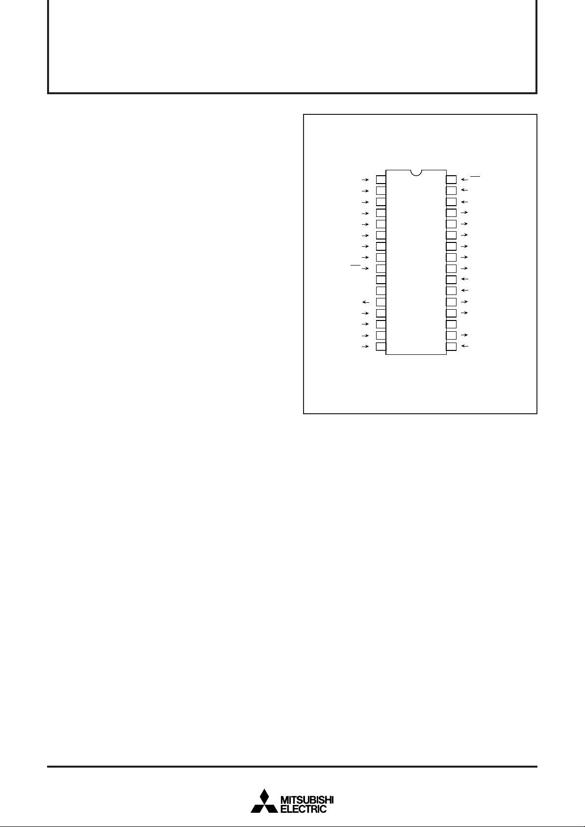
PIN CONFIGURATION (TOP VIEW)
AD0
AD1
AD2
AD3
AD4
AD5
AD6
AD7
AC
V
DD1
V
CVIDEO
LECHA
LEBK
CVIN
HOR
1
2
3
4
5
6
7
8
9
10
11
SS
12
13
14
15
16
M35060-XXXSP
32
CS
SCK
31
30
TESTA
29
P5
P4
28
27
P3
26
P2
25
P1
24
P0
TESTB
23
OSCIN
22
21
OSCOUT
20
LP2
V
DD2
19
18
LP1
17
VREF
Outline 32P4B
REV.1.1

PIN DESCRIPTION
Pin name
AD0~AD7
AC
VDD1
VSS
CVIDEO
LECHA
LEBK
CVIN
HOR
VREF
LP1
VDD2
LP2
OSCOUT
OSCIN
TESTB
P0
P1
P2
P3
P4
P5
TESTA
SCK
CS
Parallel data input
Auto-clear input
Power pin
Earthing pin
Composite video
signal output
Character level input
Black level input
Composite video
signal input
Synchronous signal
input
Slice level input
Filter output 1
Power pin
Filter output 2
The pins for attaching an external oscillator circuit for genera-
ting the synchronization signal.
Test input
Port output
Port output
Port output
Port output
Port output
Port output
Test input
Clock input for data
input
Chip select input
Input/Output
Input
Input
—
—
Output
Input
Input
Input
Input
Input
Output
—
Output
Output
Input
Input
Output
Output
Output
Output
Output
Output
Input
Input
Input
MITSUBISHI MICROCOMPUTERS
M35060-XXXSP
SCREEN CHARACTER and PATTERN DISPLAY CONTROLLERS
FunctionSymbol
These input pins determine address and data of the Display RAM, Control RAM, and
Overlay RAM (SYRAM) by 8-bit parallel. Hysteresis input is required.
When this input pin transitions from “H” to “L”, the device is reset. Built-in a pull-up
resistor. Hysteresis input is required.
Digital power supply pin. This pin must be connected to + 5V.
Ground pin. This pin must be connected to 0V.
This pin outputs the composite video signal. The output signal is 2Vp-p. In superim-
pose mode, this pin’s signal consists of the OSD signal combined with the input
composite signal CVIN.
This input pin is used for controlling the “white” character color level of the OSD signal.
This input pin is used for controlling the “black” character color level of the OSD signal.
This input pin is used for the superimpose mode. An external composite signal may be
input through this pin and mixed with the internally generated OSD signal.
This input pin is used to input the same signal as CVIN. The horizontal and vertical
sync signals are then extracted internally within the device.
This input pin is used to determine the slice voltage for extracting the sync signals from
the video composite signal.
This is filter output pin 1.
Analog power supply pin. This pin must be connected to +5V.
This is filter output pin 2.
These are the pins for attaching an external oscillator circuit for generating the
synchronization signal:
NTSC (3.580MHz), PAL (4.434MHz), M-PAL (3.576MHz).
Factory test pin. The pin must be connected to GND.
This output pin can be configured to port P0 or YM output.
This output pin can be configured to port P1 or BLNK output.
This output pin can be configured to port P2 or B output.
This output pin can be configured to port P3 or G output.
This output pin can be configured to port P4 or R output.
This output pin can be configured to port P5 or CSYN output.
Factory test pin. The pin must be connected to GND.
This pin is enabled when the CS pin is “L”. Data input to pins AD0 to AD7 is latched at
the rising edge of this signal. This pin is hysteresis input.
This is chip selection input pin. When this pin is “L”, transmission is enabled. This pin is
hysteresis input.
2
MITSUBISHI MICROCOMPUTERS
Write access
control
Read access
control
Display
position
detection
Timing
generator
Sync
separation
Vsync
separation
Synchronous
correction circuit
Quadruple
frequency circuit
Display control registerDisplay RAM
Character
Pattern ROM
SYRAM
Blinking
Shift
TESTB
CVIN
LEBK
LECHA
CVIDEO
LP1
OSCOUT
OSCIN
LP2
SCK CS
TESTA HOR
VREF
P0
/YM
P1
/BLNK
P2
/B
P3
/G
P4
/R
P5
/CSYN
Port output/Selection
Display control
Sync
generation
Video signal
output
NTSC, PAL,
M-PAL
V
DD2
V
SS
AC
AD0
AD1
AD2
AD3
AD4
AD5
AD6
AD7
3231
30
16
17
18
21
22
20
23
15
14
13
12
292827
262524
9
1119
8
7
6
5
4
3
2
1
V
DD1
10
Input control circuit
M35060-XXXSP
SCREEN CHARACTER and PATTERN DISPLAY CONTROLLERS
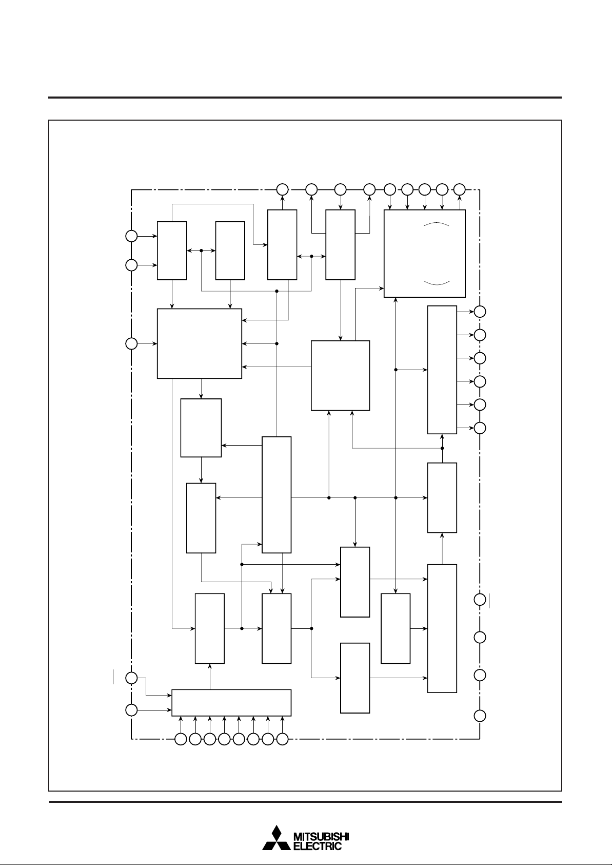
BLOCK DIAGRAM
3
MITSUBISHI MICROCOMPUTERS
M35060-XXXSP
SCREEN CHARACTER and PATTERN DISPLAY CONTROLLERS
MEMORY CONSTRUCTION
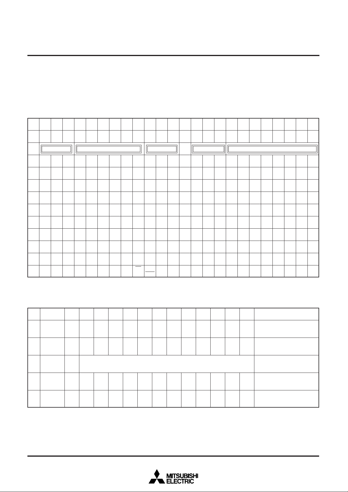
Address 00016 to 2A716 are assigned to the display RAM, 2A816 to
2B016 are assigned to the display control registers and 30016 to
6EC16 are assigned to SYRAM.
Table 1 The memory constitution of display RAM and register
add-
DA17
DA16
DA15
DA14
DA13
ress
000
16
SB
SG
SR
SYC5
~
SY color setting
2A7
16
SB
SG
SR
SYC5
TEST
TEST
2A8
16
–
3
2A9
16
–
–
2AA
16
–
–
2AB
16
–
–
2AC
16
–
–
2AD
2AE
16
2AF
16
2B0
16
TESTn (n = number) is MITSUBISHI test memory. Set 0 to all bits.
TEST
16
–
23
–
–
PC7
PC6
TEST
–
19
2
–
–
TEST
26
–
TEST
22
–
PC5
TEST
18
TEST
1
BLINK
3
TEST
12
TEST
25
TEST
21
SERS
3
–
PC4
TEST
17
DA12
SYC4
SYC3
SYRAM setting
SYC4
SYC3
TEST
TEST
0
11
BLINK
BLINK
2
1
TEST
EQP
20
PHASE
PHASE
2
1
LINE
LINE
B
G
SERS
SERS
2
1
SEND
–
4
PC3
PC2
TEST
LEVEL
24
2
DA11
SYC2
SYC2
TEST
10
BLINK
0
HIDE
PHASE
0
LINE
R
SERS
0
SEND
3
PC1
LEVEL
1
DA10
SYC1
SYC1
HP8
HSZ
16
VSZ
16
DSP0
16
DSP1
16
ERS
16
SEND
2
PC0
LEVEL
0
DAF
DAE
SYC0
BB
Raster color setting
SYC0
BB
HP7
HP6
HSZ
HSZ
15
14
VSZ
VSZ
15
14
DSP0
DSP0
15
14
DSP1
DSP1
15
14
ERS
ERS
15
14
SEND
SEND
1
0
SRAND
ALL24
2
INT
PAL
NON
NTSC
DAD
BG
BG
HP5
HSZ
13
VSZ
13
DSP0
13
DSP1
13
ERS
13
SST
4
SRAND
1
MPAL
The internal circuit is reset and all display control registers (address
2A816 to 2B016) are set to “0”. The memory constitution of display
RAM and register is shown in Figure 1 and the memory constitution
of SYRAM is shown in Figure 2.
DAC
DAB
DAA
DA9
DA8
DA7
DA6
BR
BR
HP4
HSZ
12
VSZ
12
DSP0
12
DSP1
12
ERS
12
SST
3
SRAND
0
PALH
BLINK
CB
CG
BLINK
Character color setting
BLINK
CB
CG
HP3
HP2
HP1
HSZ
HSZ
10
VSZ
10
DSP0
10
DSP1
10
ERS
10
SST
1
PTD
4
TEST
15
HSZ
9
VSZ
9
DSP0
09
DSP1
09
ERS
9
SST
0
PTD
3
SEPV1
11
VSZ
11
DSP0
11
DSP1
11
ERS
11
SST
2
PTD
5
TEST
16
CR
CR
HP0
HSZ
8
VSZ
8
DSP0
08
DSP1
08
ERS
8
SLIN
4
PTD
2
SEPV0
C7
C7
VP7
HSZ
7
VSZ
7
DSP0
07
DSP1
07
ERS
7
SLIN
3
PTD
1
BLK
C6
C6
VP6
HSZ
6
VSZ
6
DSP0
06
DSP1
06
ERS
6
SLIN
2
PTD
0
–
DA5
C5
C5
VP5
HSZ
VSZ
DSP0
05
DSP1
05
ERS
SLIN
PTC
5
DSP
ONV
Character setting
5
5
5
1
DA4
C4
C4
VP4
HSZ
4
VSZ
4
DSP0
04
DSP1
04
ERS
4
SLIN
0
PTC
4
DSP
ON
DA3
C3
C3
VP3
HSZ
3
VSZ
3
DSP0
03
DSP1
03
ERS
3
SBIT
3
PTC
3
–
DA2
C2
C2
VP2
HSZ
2
VSZ
2
DSP0
02
DSP1
02
ERS
2
SBIT
2
PTC
2
SEL
COR
DA1
C1
C1
VP1
HSZ
1
VSZ
1
DSP0
01
DSP1
01
ERS
1
SBIT
1
PTC
1
–
DA0
C0
C0
VP0
HSZ
0
VSZ
0
DSP0
00
DSP1
00
ERS
0
SBIT
0
PTC
0
EX
Table 2 The memory constitution of SYRAM
address
300
16
DA17 ~ DAD
DAC
SYEX
DAB
S00B
DAA
S00A
DA9
S009
0
30C
310
16
16
SYEX
SYEX
S00B
S01B
S00A
S01A
S009
S019
0
31C
6D0
6DC
6E0
16
~~~~~
…
16
0
16
16
SYEX
……………
SYEX
SYEX
SYEX
S01B
S3DB
…………
S3DB
S3EB
S01A
S3DA
…………
S3DA
S3EA
S019
S3D9
…………
S3D9
S3E9
0
6EC
16
: Name or value changes by definite ratio.
~
: The same name or value continues.
…
SYEX
S3EB
S3EA
S3E9
DA8
S008
S008
S018
S018
S3D8
…………
S3D8
S3E8
S3E8
DA7
S007
S007
S017
S017
S3D7
……………………
S3D7
S3E7
S3E7
DA6
S006
S006
S016
S016
S3D6
…………
S3D6
S3E6
S3E6
DA5
S005
S005
S015
S015
~
S3D5
S3D5
S3E5
S3E5
DA4
S004
DA3
S003
DA2
S002
DA1
S001
DA0
S000
SYRAM code
0016
S004
S014
S003
S013
S002
S012
S001
S011
S000
S010
0116
S014
S013
S012
S011
S010
~
S3D4
S3D3
…………
…………
S3D4
S3E4
S3E4
…………
S3D3
S3E3
S3E3
S3D2
…………
S3D2
S3E2
S3E2
S3D1
…………
S3D1
S3E1
S3E1
S3D0
…………
S3D0
S3E0
S3E0
3D16
3E16
4
SCREEN CHARACTER and PATTERN DISPLAY CONTROLLERS
001 002 003 004 005 006 007 008 009 00A 00B 00C 00D 00E 00F 010 011 012 013 014 015 016 017 018 019 01A 01B 01C 01D 01E 01F 020 021 022 023 024 025 026 027000
079 07A 07B 07C 07D 07E 07F 080 081 082 083 084 085 086 087 088 089 08A 08B 08C 08D 08E 08F 090 091 092 093 094 095 096 097 098 099 09A 09B 09C 09D 09E 09F078
0A1 0A2 0A3 0A4 0A5 0A6 0A7 0A8 0A9 0AA 0AB 0AC 0AD 0AE 0AF 0B0 0B1 0B2 0B3 0B4 0B5 0B6 0B7 0B8 0B9 0BA 0BB 0BC 0BD 0BE 0BF 0C0 0C1 0C2 0C3 0C4 0C5 0C6 0C70A0
0C9 0CA0CB 0CC 0CD 0CE 0CF 0D0 0D1 0D2 0D3 0D4 0D5 0D6 0D7 0D8 0D9 0DA 0DB0DC0DD0DE 0DF 0E0 0E1 0E2 0E3 0E4 0E5 0E6 0E7 0E8 0E9 0EA 0EB0EC 0ED 0EE 0EF0C8
0F1 0F2 0F3 0F4 0F5 0F6 0F7 0F8 0F9 0FA 0FB 0FC 0FD 0FE 0FF 100 101 102 103 104 105 106 107 108 109 10A 10B 10C 10D 10E 10F 110 111 112 113 114 115 116 1170F0
141 142 143 144 145 146 147 148 149 14A 14B 14C 14D 14E 14F 150 151 152 153 154 155 156 157 158 159 15A 15B 15C 15D 15E 15F 160 161 162 163 164 165 166 167140
169 16A 16B 16C 16D 16E 16F 170 171 172 173 174 175 176 177 178 179 17A 17B 17C 17D 17E 17F 180 181 182 183 184 185 186 187 188 189 18A 18B 18C 18D 18E 18F168
1B9 1BA 1BB 1BC 1BD 1BE 1BF 1C0 1C1 1C2 1C3 1C4 1C5 1C6 1C7 1C8 1C9 1CA1CB 1CC1CD 1CE 1CF 1D0 1D1 1D2 1D3 1D4 1D5 1D6 1D7 1D8 1D9 1DA 1DB1DC1DD1DE 1DF1B8
259 25A 25B 25C 25D 25E 25F 260 261 262 263 264 265 266 267 268 269 26A 26B 26C 26D 26E 26F 270 271 272 273 274 275 276 277 278 279 27A 27B 27C 27D 27E 27F258
119 11A 11B 11C 11D 11E 11F 120 121 122 123 124 125 126 127 128 129 12A 12B 12C 12D 12E 12F 130 131 132 133 134 135 136 137 138 139 13A 13B 13C 13D 13E 13F118
191 192 193 194 195 196 197 198 199 19A 19B 19C 19D 19E 19F 1A0 1A1 1A2 1A3 1A4 1A5 1A6 1A7 1A8 1A9 1AA 1AB 1AC 1AD 1AE 1AF 1B0 1B1 1B2 1B3 1B4 1B5 1B6 1B7190
1E1 1E2 1E3 1E4 1E5 1E6 1E7 1E8 1E9 1EA 1EB 1EC 1ED 1EE 1EF 1F0 1F1 1F2 1F3 1F4 1F5 1F6 1F7 1F8 1F9 1FA 1FB 1FC 1FD 1FE 1FF 200 201 202 203 204 205 206 2071E0
231 232 233 234 235 236 237 238 239 23A 23B 23C 23D 23E 23F 240 241 242 243 244 245 246 247 248 249 24A 24B 24C 24D 24E 24F 250 251 252 253 254 255 256 257230
281 282 283 284 285 286 287 288 289 28A 28B 28C 28D 28E 28F 290 291 292 293 294 295 296 297 298 299 29A 29B 29C 29D 29E 29F 2A0 2A1 2A2 2A3 2A4 2A5 2A6 2A7280
051 052 053 054 055 056 057 058 059 05A 05B 05C 05D 05E 05F 060 061 062 063 064 065 066 067 068 069 06A 06B 06C 06D 06E 06F 070 071 072 073 074 075 076 077050
029 02A 02B 02C 02D 02E 02F 030 031 032 033 034 035 036 037 038 039 03A 03B 03C 03D 03E 03F 040 041 042 043 044 045 046 047 048 049 04A 04B 04C 04D 04E 04F028
208 209 20A 20B 20C 20D 20E 20F 210 211 212 213 214 215 216 217 218 219 21A 21B 21C 21D 21E 21F 220 221 222 223 224 225 226 227 228 229 22A 22B 22C 22D 22E 22F
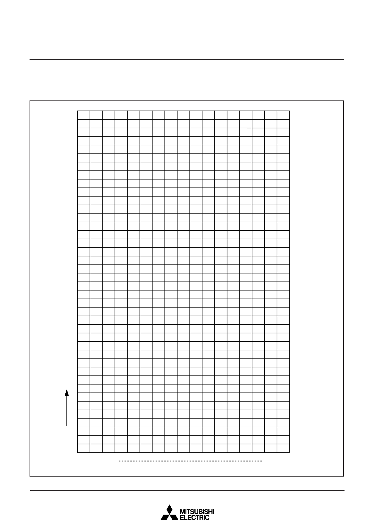
The hexadecimal numbers in the boxes show the display RAM address
Line 16
Row
Line 0
Line 1
Line 15
SCREEN CONSTITUTION
The screen lines and rows are determined from each address of the display RAM.
The screen constitution is shown in Figure 1.
MITSUBISHI MICROCOMPUTERS
M35060-XXXSP
Fig. 1 Screen constitution
5
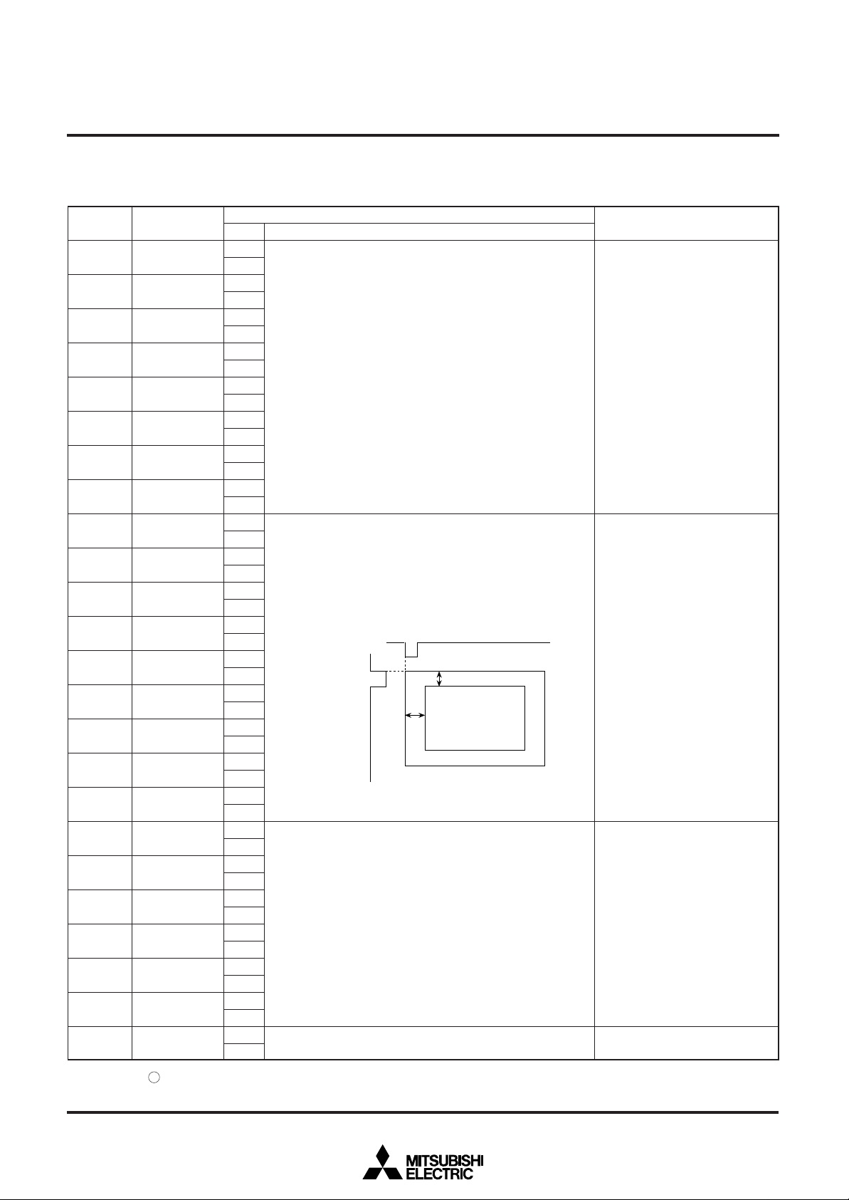
REGISTERS DESCRIPTION
(1) Address 2A816
MITSUBISHI MICROCOMPUTERS
M35060-XXXSP
SCREEN CHARACTER and PATTERN DISPLAY CONTROLLERS
DA
C
D
E
F
10
11
12
13
14
15
16
17
Register
0
1
2
3
4
5
6
7
8
9
A
B
VP0
VP1
VP2
VP3
VP4
VP5
VP6
VP7
HP0
HP1
HP2
HP3
HP4
HP5
HP6
HP7
HP8
TEST10
TEST11
TEST0
TEST1
TEST2
TEST3
—
Status
0
If VS is the vertical display start location,
1
0
VS = H ✕ ( Σ 2n VPn )
1
7
n=0
0
1
0
1
0
1
0
1
0
1
0
1
0
If HS is the horizontal display start location,
1
0
HS = T ✕ ( Σ 2n HPn + 9 )
1
8
n=0
0
1
0
1
0
1
0
1
0
1
0
1
0
1
0
Test mode (Must be cleared to 0.)
1
0
1
0
1
0
1
0
1
0
1
0
Must be cleared to 0.
1
Contents
Function
H: Cycle with the horizontal synchronizing pulse
T: Cycle with the display clock
HOR
TV screen
VS
HS
Character
displaying area
VERT
1 bit weights 1 clock.
Note: The mark__around the status value means the reset status by the “L” level is input to AC pin.
Remarks
The vertical start location is
specified using the 8 bits from
VP7 to VP0.
VP7 to VP0 < 1416 are not
available.
The horizontal start location is
specified using the 9 bits from
HP8 to HP0.
HP8 to HP0 < 1916 are not
available.
6
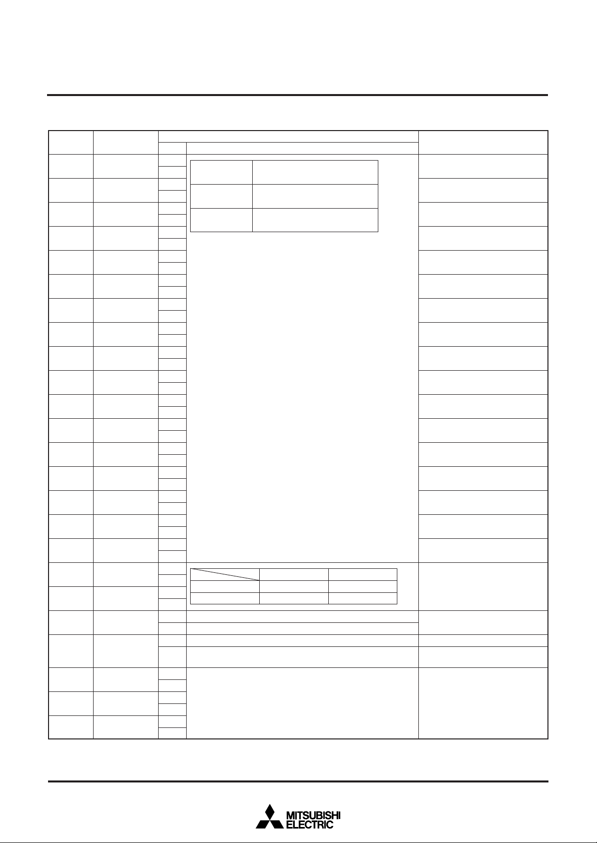
(2) Address 2A916
DA Register
0
1
2
3
4
5
6
7
8
9
A
B
C
D
E
F
10
11
12
13
14
15
16
17
HSZ0
HSZ1
HSZ2
HSZ3
HSZ4
HSZ5
HSZ6
HSZ7
HSZ8
HSZ9
HSZ10
HSZ11
HSZ12
HSZ13
HSZ14
HSZ15
HSZ16
BLINK0
BLINK1
BLINK2
BLINK3
—
—
—
SCREEN CHARACTER and PATTERN DISPLAY CONTROLLERS
Contents
Status
0
1
0
1
0
1
0
1
0
1
0
1
0
1
0
1
0
1
0
1
0
1
0
1
0
1
0
1
0
1
0
1
0
1
0
1
0
1
0
1
0
1
0
1
0
1
0
1
HSZx
0
1
BLINK1
0
1
Cycle approximately 1 second.
Cycle approximately 0.5 second.
Normal blinking
Normal character, reversed character alternation display.
Must be cleared to 0.
Horizontal direction character size
BLINK0
Function
1T/dot
2T/dot
0
Blinking OFF
Duty 50%
T: Display clock
1
Duty 25%
Duty 75%
MITSUBISHI MICROCOMPUTERS
M35060-XXXSP
Remarks
Set to line 0 of display RAM
Set to line 1 of display RAM
Set to line 2 of display RAM
Set to line 3 of display RAM
Set to line 4 of display RAM
Set to line 5 of display RAM
Set to line 6 of display RAM
Set to line 7 of display RAM
Set to line 8 of display RAM
Set to line 9 of display RAM
Set to line 10 of display RAM
Set to line 11 of display RAM
Set to line 12 of display RAM
Set to line 13 of display RAM
Set to line 14 of display RAM
Set to line 15 of display RAM
Set to line 16 of display RAM
Blinking duty ratio can be altered.
Blinking cycle can be altered.
Character is in flashing state.
Character is always displayed
(normal character, reversed character).
7
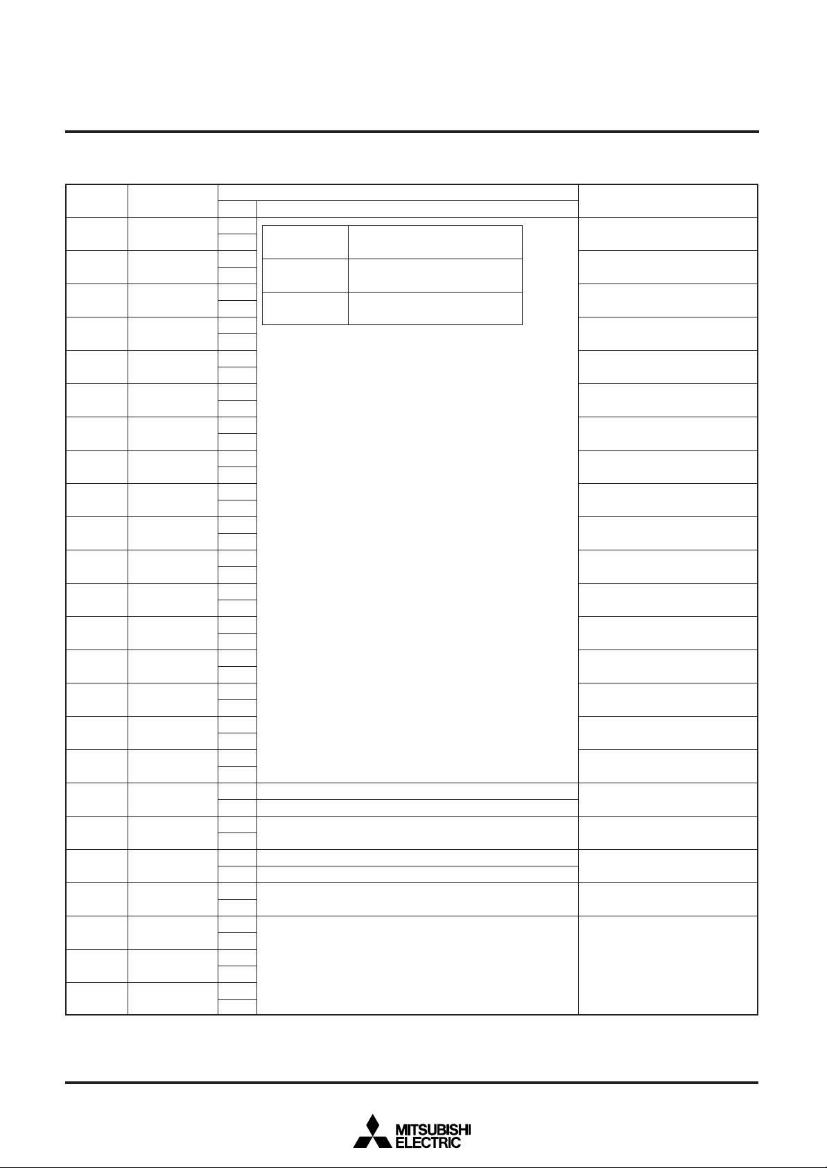
(3) Address 2AA16
MITSUBISHI MICROCOMPUTERS
M35060-XXXSP
SCREEN CHARACTER and PATTERN DISPLAY CONTROLLERS
DA Register
0
1
2
3
4
5
6
7
8
9
A
B
C
D
E
F
10
11
12
13
14
15
16
17
VSZ0
VSZ1
VSZ2
VSZ3
VSZ4
VSZ5
VSZ6
VSZ7
VSZ8
VSZ9
VSZ10
VSZ11
VSZ12
VSZ13
VSZ14
VSZ15
VSZ16
HIDE
TEST20
EQP
TEST12
—
—
—
Status
0
1
0
1
0
1
0
1
0
1
0
1
0
1
0
1
0
1
0
1
0
1
0
1
0
1
0
1
0
1
0
1
0
1
0
1
0
1
0
1
0
1
0
1
0
1
0
1
VSZx
0
1
SYRAM writting over
SYRAM writting over or character erasing
Test mode (Must be cleared to 0.)
It does not include equivalent pulse.
It includes equivalent pulse.
Test mode (Must be cleared to 0.)
Must be cleared to 0.
Vertical direction character size
H: Horizontal synchronous pulse
Contents
Function
1H/dot
2H/dot
Remarks
Set to line 0 of display RAM
Set to line 1 of display RAM
Set to line 2 of display RAM
Set to line 3 of display RAM
Set to line 4 of display RAM
Set to line 5 of display RAM
Set to line 6 of display RAM
Set to line 7 of display RAM
Set to line 8 of display RAM
Set to line 9 of display RAM
Set to line 10 of display RAM
Set to line 11 of display RAM
Set to line 12 of display RAM
Set to line 13 of display RAM
Set to line 14 of display RAM
Set to line 15 of display RAM
Set to line 16 of display RAM
Decided by register LINER, G and
B or DAC bit of SYRAM.
8
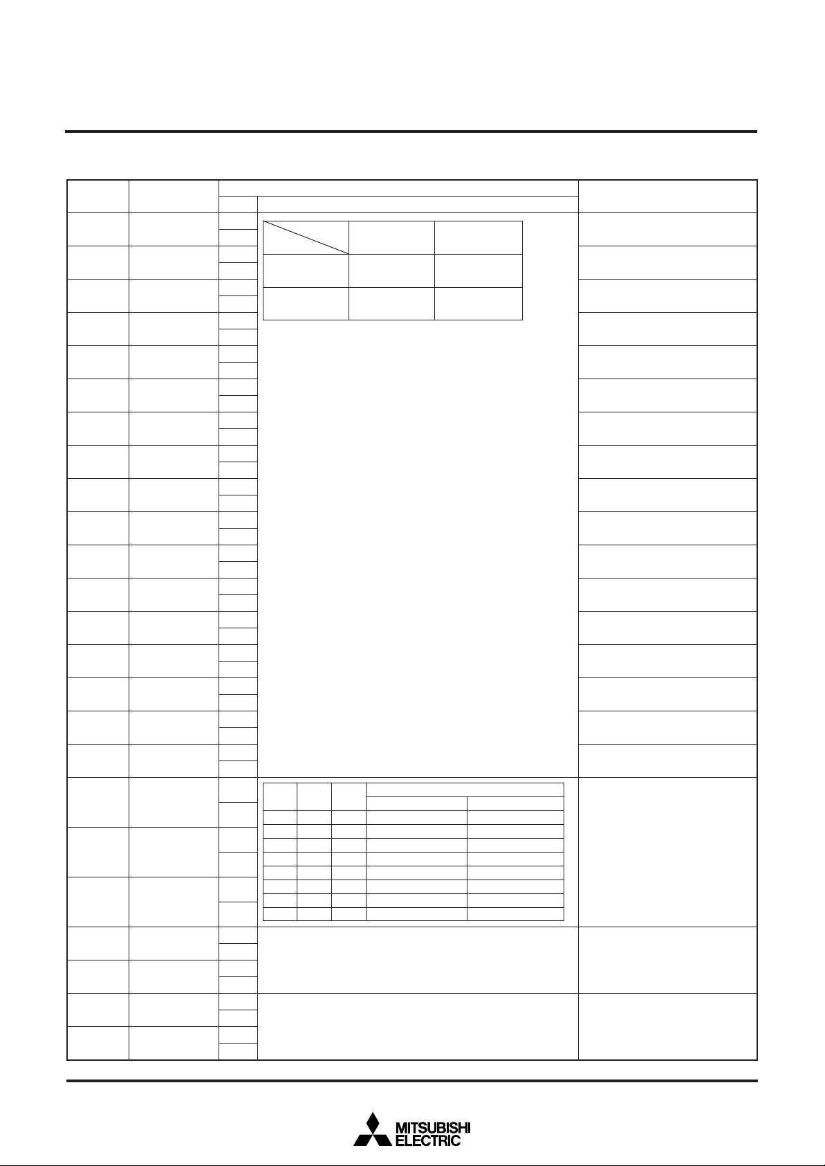
(4) Address 2AB16
DA Register
0
1
2
3
4
5
6
7
8
9
A
B
C
D
E
F
10
11
12
13
14
15
16
17
DSP0 00
DSP0 01
DSP0 02
DSP0 03
DSP0 04
DSP0 05
DSP0 06
DSP0 07
DSP0 08
DSP0 09
DSP0 10
DSP0 11
DSP0 12
DSP0 13
DSP0 14
DSP0 15
DSP0 16
PHASE 0
PHASE 1
PHASE 2
TEST25
TEST26
MITSUBISHI MICROCOMPUTERS
M35060-XXXSP
SCREEN CHARACTER and PATTERN DISPLAY CONTROLLERS
Contents
Status
0
1
0
1
0
1
0
1
0
1
0
1
0
1
0
1
0
1
0
1
0
1
0
1
0
1
0
1
0
1
0
1
0
1
0
1
0
1
0
1
0
1
0
1
—
—
0
1
0
1
DSP0XX
DSP1XX
0
1
Set by combination of DSP0XX (address 2AB16 and DSP1XX)
and DSP1XX (address 2AC16).
At internal synchronous mode (EX = 1), display monitor signal
area is all blanking signal (BLNK output) area.
Note: For halftone display, it is necessary to input the external
composite video signal to the CVIN terminal, and externally connect a 100 to 200 resistor in series.
However, the halftone display is possible only with superimposed displays.
PHASE
PHASE
PHASE
2
0
0
0
0
1
1
1
1
Test mode (Must be cleared to 0.)
Must be cleared to 0.
0
1
0
0
1
0
0
1
1
1
0
0
1
0
0
1
1
1
Function
0
Character
Matrix-outline
SELCOR=0
Black
Red
Green
Yellow
Blue
Magenta
Cyan
White
1
Border
Halftone
(Note)
Color
SELCOR=1
Black
Red–2
Green–2
Yellow
Gray
Yellow–2
Cyan
White
Set to line 0 of display RAM
Set to line 1 of display RAM
Set to line 2 of display RAM
Set to line 3 of display RAM
Set to line 4 of display RAM
Set to line 5 of display RAM
Set to line 6 of display RAM
Set to line 7 of display RAM
Set to line 8 of display RAM
Set to line 9 of display RAM
Set to line 10 of display RAM
Set to line 11 of display RAM
Set to line 12 of display RAM
Set to line 13 of display RAM
Set to line 14 of display RAM
Set to line 15 of display RAM
Set to line 16 of display RAM
Raster color setting.
Refer Fig 3, 4 about phase angle.
Remarks
9
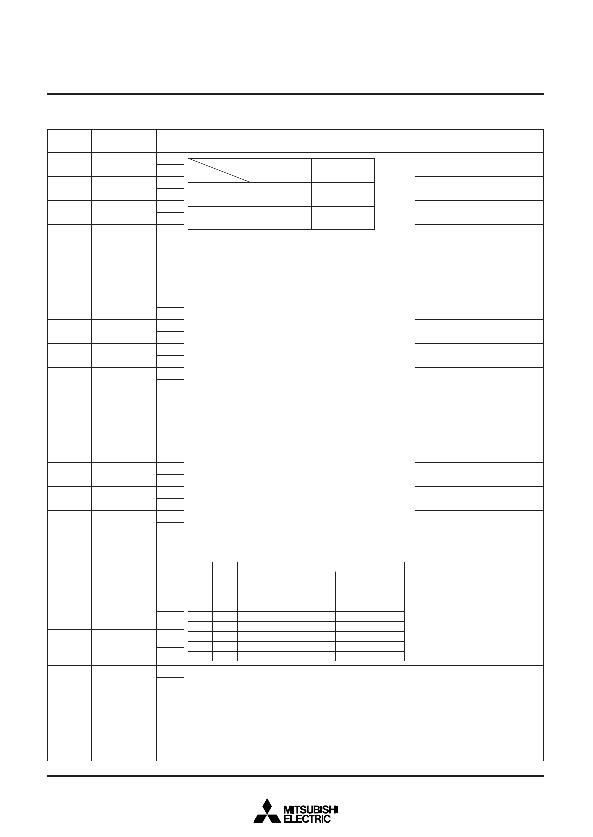
(5) Address 2AC16
DA Register
0
1
2
3
4
5
6
7
8
9
A
B
C
D
E
F
10
11
12
13
14
15
16
17
DSP1 00
DSP1 01
DSP1 02
DSP1 03
DSP1 04
DSP1 05
DSP1 06
DSP1 07
DSP1 08
DSP1 09
DSP1 10
DSP1 11
DSP1 12
DSP1 13
DSP1 14
DSP1 15
DSP1 16
LINER
LINEG
LINEB
TEST21
—
—
—
SCREEN CHARACTER and PATTERN DISPLAY CONTROLLERS
Contents
Status
0
1
0
1
0
1
0
1
0
1
0
1
0
1
0
1
0
1
0
1
0
1
0
1
0
1
0
1
0
1
0
1
0
1
0
1
0
1
0
1
0
1
0
1
0
1
0
1
DSP0XX
DSP1XX
0
1
Set by combination of DSP0XX (address 2AB16 and DSP1XX)
and DSP1XX (address 2AC16).
At internal synchronous mode (EX = 1), display monitor signal
area is all blanking signal (BLNK output) area.
Note: For halftone display, it is necessary to input the external
composite video signal to the CVIN terminal, and externally connect a 100 to 200 resistor in series.
However, the halftone display is possible only with superimposed displays.
LINE
LINE
LINE
B
0
0
0
0
1
1
1
1
Test mode (Must be cleared to 0.)
Must be cleared to 0.
R
G
0
0
1
0
0
1
1
1
0
0
1
0
0
1
1
1
Function
0
Character
Matrix-outline
SELCOR=0
Black
Red
Green
Yellow
Blue
Magenta
Cyan
White
1
Border
Halftone
(Note)
Color
SELCOR=1
Black
Red–2
Green–2
Yellow
Gray
Yellow–2
Cyan
White
MITSUBISHI MICROCOMPUTERS
M35060-XXXSP
Remarks
Set to line 0 of display RAM
Set to line 1 of display RAM
Set to line 2 of display RAM
Set to line 3 of display RAM
Set to line 4 of display RAM
Set to line 5 of display RAM
Set to line 6 of display RAM
Set to line 7 of display RAM
Set to line 8 of display RAM
Set to line 9 of display RAM
Set to line 10 of display RAM
Set to line 11 of display RAM
Set to line 12 of display RAM
Set to line 13 of display RAM
Set to line 14 of display RAM
Set to line 15 of display RAM
Set to line 16 of display RAM
SYRAM color setting.
Color is decided by DAC bit
(SYEX) of SYRAM or HIDE
register.
Refer Fig. 3, 4 about phase angle.
10
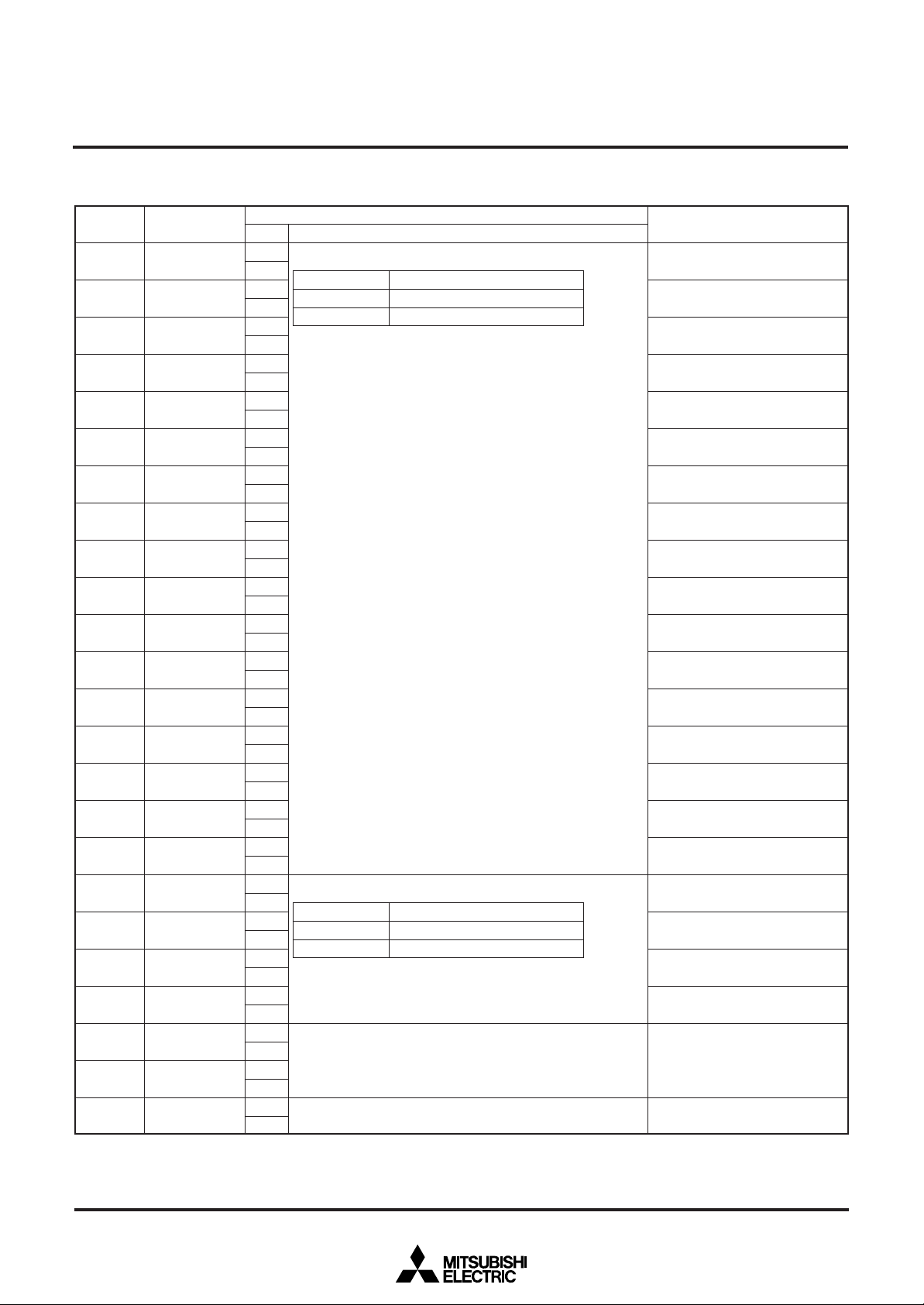
(6) Address 2AD16
MITSUBISHI MICROCOMPUTERS
M35060-XXXSP
SCREEN CHARACTER and PATTERN DISPLAY CONTROLLERS
DA Register
0
1
2
3
4
5
6
7
8
9
A
B
C
D
E
F
10
11
12
13
14
15
16
17
ERS0
ERS1
ERS2
ERS3
ERS4
ERS5
ERS6
ERS7
ERS8
ERS9
ERS10
ERS11
ERS12
ERS13
ERS14
ERS15
ERS16
SERS0
SERS1
SERS2
SERS3
TEST22
TEST23
—
Status
0
1
0
1
0
1
0
1
0
1
0
1
0
1
0
1
0
1
0
1
0
1
0
1
0
1
0
1
0
1
0
1
0
1
0
1
0
1
0
1
0
1
0
1
0
1
0
1
Contents
Function
Erase display RAM
ERSx
0
1
It is unnecessary to reset these registers to “0”.
Multiple settings of ERSn is not allowed.
Erase SYRAM
SERSx
0
1
It is unnecessary to reset these registers to “0”.
Multiple settings of SERSn is not allowed.
Test mode (Must be cleared to 0.)
Must be cleared to 0.
RAM erase
do erase
do not erase
SYRAM erase
do erase
do not erase
Remarks
Set to line 0 of display RAM
Set to line 1 of display RAM
Set to line 2 of display RAM
Set to line 3 of display RAM
Set to line 4 of display RAM
Set to line 5 of display RAM
Set to line 6 of display RAM
Set to line 7 of display RAM
Set to line 8 of display RAM
Set to line 9 of display RAM
Set to line 10 of display RAM
Set to line 11 of display RAM
Set to line 12 of display RAM
Set to line 13 of display RAM
Set to line 14 of display RAM
Set to line 15 of display RAM
Set to line 16 of display RAM
Set to SYRAM code 0016 to 0F16
Set to SYRAM code 1016 to 1F16
Set to SYRAM code 2016 to 2F16
Set to SYRAM code 3016 to 3E16
11

(7) Address 2AE16
DA
0
1
2
3
4
5
6
7
8
9
A
B
C
D
E
F
10
11
12
13
14
15
16
17
Note: When the scrolling on, set the ratio which will be SC < SB < SD.
Register
SBIT0
SBIT1
SBIT2
SBIT3
SLIN0
SLIN1
SLIN2
SLIN3
SLIN4
SST0
SST1
SST2
SST3
SST4
SEND0
SEND1
SEND2
SEND3
SEND4
—
—
—
—
—
Status
0
Set display start bit of scroll block:
1
0
1
3
SA = Σ 2n (SBITn)
n=0
0
1
0
1
0
Set display start line of scroll block:
1
0
1
4
SB = Σ 2n (SLINn)
n=0
0
1
0
1
0
1
0
Set start line of scroll block
1
(last line number of the fixed block 1):
0
1
4
SC = Σ 2n (SSTn)
n=0
0
1
0
1
0
1
0
Set start line of fixed block 2
1
(last line number of the scroll block):
0
1
0
4
SD = Σ 2n (SENDn)
n=0
1
0
1
0
1
0
Must be cleared to 0.
1
0
1
0
1
0
1
0
1
MITSUBISHI MICROCOMPUTERS
M35060-XXXSP
SCREEN CHARACTER and PATTERN DISPLAY CONTROLLERS
Contents
Function
Setting valid
invalid
Setting valid
invalid
Setting valid
invalid
When the scrolling on
setting valid SD = 2 to 17
invalid SD = 18 to 31
When the scrolling off
set SD = 0
SD > SC + 2
Remarks
SA = 0 to 12
SA = 13 to 15
SB = 0 to 16
SB = 17 to 31
SC = 0 to 15
SC = 16 to 31
12
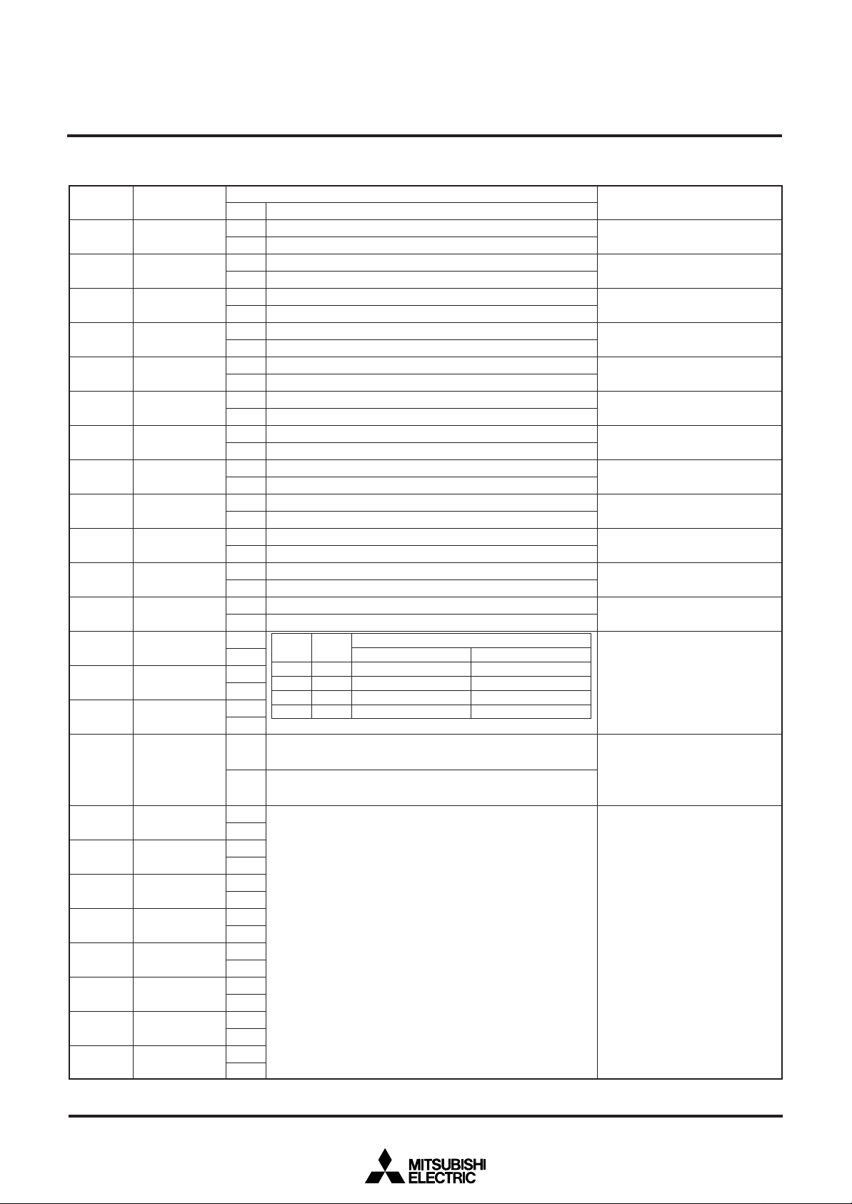
SCREEN CHARACTER and PATTERN DISPLAY CONTROLLERS
(8) Address 2AF16
DA Register
0
1
2
3
4
5
6
7
8
9
A
B
C
D
E
F
10
11
12
13
14
15
16
17
Note: At EX (address 2B016) = “0” (external synchronous), setting “1” of ALL24 register is not available.
Refer Fig. 2 about PTC0 to 5, PTD0 to 5.
PTC0
PTC1
PTC2
PTC3
PTC4
PTC5
PTD0
PTD1
PTD2
PTD3
PTD4
PTD5
SRAND0
SRAND1
SRAND2
ALL24
PC0
PC1
PC2
PC3
PC4
PC5
PC6
PC7
Status
0
1
0
1
0
1
0
1
0
1
0
1
0
1
0
1
0
1
0
1
0
1
0
1
0
1
0
1
0
1
0
1
0
1
0
1
0
1
0
1
0
1
0
1
0
1
0
1
Port P0 output
YM output
Port P1 output
BLNK output
Port P2 output
B output
Port P3 output
G output
Port P4 output
R output
Port P5 output
CSYN output
When port output: 0 output, when YM output: negative polarity.
When port output: 1 output, when YM output: polarity.
When port output: 0 output, when BLNK output: negative polarity.
When port output: 1 output, when BLNK output: polarity.
When port output: 0 output, when B output: negative polarity.
When port output: 1 output, when B output: polarity.
When port output: 0 output, when G output: negative polarity.
When port output: 1 output, when G output: polarity.
When port output: 0 output, when R output: negative polarity.
When port output: 1 output, when R output: polarity.
When port output: 0 output, when CSYN output: negative polarity.
When port output: 1 output, when CSYN output: polarity.
SRAND1SRAND
Vertical direction is 1 dot only.
Blanking with all 40 characters in matrix-outline mode
Horizontal display period fully blanked with all characters in
matrix-outline size.
Display frequency fT control
fT = fH ✕ { Σ (2nPCn) + 512 }
0
0
0
0
1
1
0
1
1
7
n=0
Contents
Function
SRAND2
0
Complete border = 1 dot
Complete border = 2 dot
Complete border = 3 dot
Complete border = 4 dot
Right and dot border = 1 dot
Right and dot border = 2 dot
Right and dot border = 3 dot
Right and dot border = 4 dot
MITSUBISHI MICROCOMPUTERS
M35060-XXXSP
Remarks
Select P0 pin
Select P1 pin
Select P2 pin
Select P3 pin
Select P4 pin
Select P5 pin
Select data of P0 pin
Select data of P1 pin
Select data of P2 pin
Select data of P3 pin
Select data of P4 pin
Select data of P5 pin
1
Condition of border display is
changeable.
Horizontal display range can be
altered when all characters are in
matrix-outline size.
At external synchronous, set to 0.
Operation of character code FF16
becomes ineffective.
PC7 to PC0 < 3616,
PC7 to PC0 > C616 is not
available.
13
 Loading...