

MITSUBISHI MICROCOMPUTERS
M35054-XXXFP/M35055-XXXFP
SCREEN CHARACTER and PATTERN DISPLAY CONTROLLERS
DESCRIPTION
The M35054-XXXFP and M35055-XXXFP are TV screen display control IC which can be used to display information such as number of
channels, the date and messages and program schedules on the TV
screen.
In particular, owing to the built-in SYNC-SEP (synchronous separation) circuit, the synchronous correction circuit, external circuits can
be decrease and character turbulence that occurs when superimposing can be reduced. The processor is suitable for AV systems
such as VTRs, LDs, and so on.
It is a silicon gate CMOS process and M35054-XXXFP and M35055XXXFP are housed in a 20-pin shrink SOP package.
For M35054-001FP/M35055-001FP that are a standard ROM versions of M35054-XXXFP/M35055-XXXFP respectively, the character pattern is also mentioned.
FEATURES
Screen composition .............................. 24 characters ✕ 10 lines,
•
Number of characters displayed ..................................240 (Max.)
•
Character composition ..................................... 12 ✕ 18 dot matrix
•
Characters available .............................128 characters (M35054)
•
Character sizes available....................4 (horizontal) ✕ 4 (vertical)
•
Display locations available
•
Horizontal direction............................................... 240 locations
Vertical direction ................................................... 256 locations
Blinking .................................................................Character units
•
Cycle : approximately 1 second, or approximately 0.5 seconds
Duty : 25%, 50%, or 75%
Data input..............................By the serial input function (16 bits)
•
Coloring
•
Background coloring (composite video signal)
Blanking
•
Total blanking (14 ✕ 18 dots)
Border size blanking
Character size blanking
Synchronizing signal
•
Composite synchronizing signal generation
(PAL, NTSC, M-PAL)
2 output ports (1 digital line)
•
Oscillation stop function
•
It is possible to stop the oscillation for synchronizing signal
generation
Built-in half-tone display function
•
Built-in reversed character display function
•
Built-in synchronous correction circuit
•
Built-in synchronous separation circuit
•
............................. 256 characters (M35055)
32 characters ✕ 7 lines
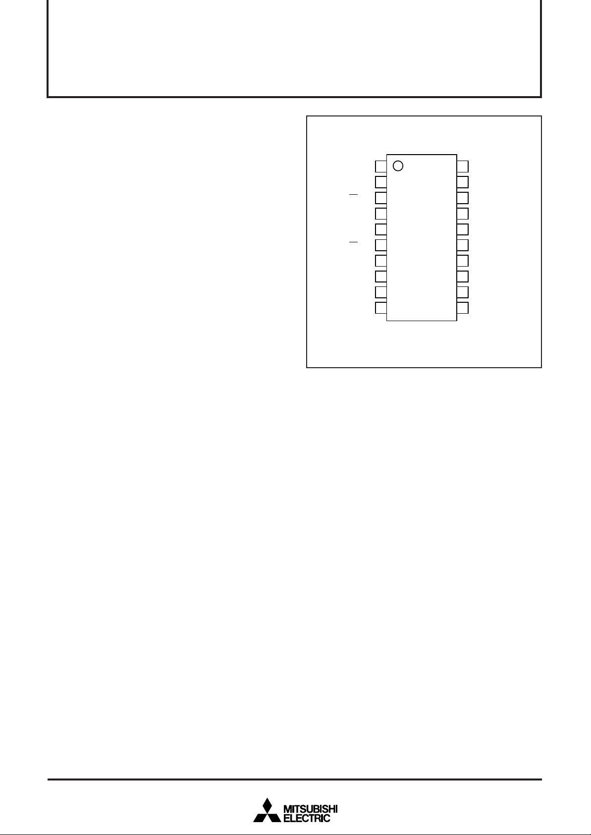
PIN CONFIGURATION (TOP VIEW)
CP1
TESTA
CS
SCK
SIN
AC
V
DD2
CVIDEO
LECHA
CVIN
1
←
2
3
→
4
→
5
→
6
→
7
8
←
9
→
10
→
Outline 20P2Q-A
M35054-XXXFP
M35055-XXXFP
20
19
←
18
→
17
←
16
15
→
14
→
13
12
11
DD1
V
HOR
CP2
OSCIN
V
SS
P1
P0
TESTB
TESTC
V
SS
APPLICATION
TV, VCR, Movie
REV.1.1
PIN DESCRIPTION
Symbol
OSC1
TESTA
__
CS
SCK
SIN
__
AC
VDD2
CVIDEO
LECHA
CVIN
VSS
TESTC
TESTB
P0
P1
VSS
OSCIN
CP2
HOR
VDD1
Pin name
Clock input
Test pin input
Chip select input
Serial clock input
Serial data input
Auto-clear input
Power pin
Composite video
signal output
Character level input
Composite video
signal input
Earthing pin
Test pin output
Test pin input
Port P0 output
Port P1 output
Earthing pin
fSC input pin for
synchronous signal
generation
Filter output
Horizontal synchro-
nizing signal input
Power pin
Input/
Output
Input
—
Input
Input
Input
Input
—
Output
Input
Input
—
—
—
Output
Output
—
Input
Output
Input
—
MITSUBISHI MICROCOMPUTERS
M35054-XXXFP/M35055-XXXFP
SCREEN CHARACTER and PATTERN DISPLAY CONTROLLERS
Function
This is the filter output pin 1.
This is the pin for test. Connect this pin to GND during normal operation.
This is the chip select pin, and when serial data transmission is being carried out, it goes
to “L”. Hysteresis input. Built-in pull-up resistor.
__
When CS pin is “L”, SIN serial data is taken in when SCK rises. Hysteresis input. Built-in
pull-up resistor.
This is the pin for serial input of data and addresses for the display control register and
the display data memory. Hysteresis input. Built-in pull-up resistor.
When “L”, this pin resets the internal IC circuit. Hysteresis input. Built-in pull-up resistor.
Please connect to +5V with the analog circuit power pin.
This is the output pin for composite video signals. It outputs 2VP-P composite video
signals. In superimpose mode, character output etc. is superimposed on the external
composite video signals from CVIN.
This is the input pin which determines the “white” character color level in the composite
video signal.
This is the input pin for external composite video signals. In superimpose mode, character
output etc. is superimposed on these external composite video signals.
Please connect to GND using circuit earthing pin.
This is the pin for test. Open this pin during normal operation.
This is the pin for test. Connect this pin to GND during normal operation.
This pin outputs the port output or BLNK1 (character background) signal.
This pin outputs the port output or CO1(character) signal.
Please connect to GND using circuit earthing pin (Analog side).
This is the input pin for the sub-carrier frequency (fSC) for generating a synchronous
signal.
A frequency of 3.580MHz is needed for NTSC, and a frequency of 4.434MHz in needed
for PAL and 3.576MHz is needed for M-PAL.
Filter output pin 2.
This is the input pin for external composite video signals. This pin inputs the external
video signal clamped sync-chip to 1.5V, and internally carries out synchronous separation.
Please connect to +5V with the digital circuit power pin.
2
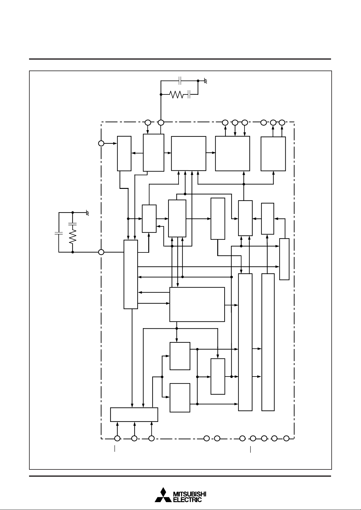
MITSUBISHI MICROCOMPUTERS
Data
control
circuit
Address
control
circuit
Display control
register
Display RAM
Display character ROM
Timing
generator
Blinking circuit
Shift register
Display control
circuit
Reading address
control circuit
H counter
NTSC
PAL
M-PAL
video output
circuit
Timing
generator
SYNC-SEP
circuit
3.580MHz(NTSC)
4.434MHz(PAL)
3.576MHz(M-PAL)
TESTA
TESTB
Port output
circuit
Clock oscillation circuit
SCK
SIN
CS
CVIDEO
CVIN
LECHA
V
DD1
AC
V
SS
V
DD2
HOR
P0
P1
CP1
V
SS
TESTC
OSCIN
CP2
I/O control circuit
Oscillation circuit
for synchronizing
signal generation
Display location
detection circuit
7
16
11
20
6
13
2
5
4
3
119
17
18
8
10
9
12
14
15
M35054-XXXFP/M35055-XXXFP
SCREEN CHARACTER and PATTERN DISPLAY CONTROLLERS
BLOCK DIAGRAM
3
SCREEN CHARACTER and PATTERN DISPLAY CONTROLLERS
MEMORY CONSTITUTION
Address 0016 to EF16 are assigned to the display RAM, address F016
to F816 are assigned to the display control registers.
The internal circuit is reset and all display control registers (address
F016 to F816) are set to “0” and display RAM (address 0016 to EF16)
are RAM erased when the AC pin level is “L”.
When using M35054-XXXFP, set “0” in any of DA7, DAD through
DAF of addresses 0016 through EF16, and of DAE and DAF of ad-
Address
00
16
FED
000
__
DADA DA
DA DA DA DA DA DA DA DA DA DA DA DA DA
CBA9876543210
REV BLINK B G R C6 C5 C4 C3 C2 C1 C0
MITSUBISHI MICROCOMPUTERS
M35054-XXXFP/M35055-XXXFP
dresses F016 through F816.
Setting the blank code “FF16” as a character code is an exception.
When using M35055-XXXFP, set “0” in any of DAD through DAF of
addresses 0016 through EF16, and of DAE and DAF of addresses
F016 through F816.
TESTn (n : a number) is MITSUBISHI test memory, so be sure to
observe the setting conditions.
0
EF
F0
F1
F2
F3
F4
F5
F6
F7
F8
Display RAM
16
16
16
16
16
16
16
16
Display control register
16
16
Reverse
000
0 0 TEST15
0 0 TEST21
0 0 TEST27
0 0 TEST33
0 0 TEST36
0 0 TEST42
0 0 TEST43
0 0 TEST46
0 0 LEVEL1
Blinking
REV BLINK C6 C5 C4 C3 C2 C1 C0
TEST13 TEST12 SYSEP1 SYSEP0 SEPV1 SEPV0 PTD1 PTD0 PTC1 PTC0
TEST14
TEST20
TEST19
TEST26
TEST25
TEST32
TEST31
TEST35 TEST34 SPACE DSP9 DSP8 DSP7 DSP6 DSP5 DSP4 DSP3 DSP2 DSP1 DSP0
TEST40
TEST41 TEST39 TEST38 TEST37 EQP PALH MPAL INT/NON N/P BLINK2 BLINK1 BLINK0
TEST2 TEST1 TEST0 LBLACK LIN24/32 BLKHF BB BG BR LEVEL0 PHASE2 PHASE1 PHASE0
TEST45
RGBON TEST44 CL17/18 CBLINK CURS7 CURS6 CURS5 CURS4 CURS3 CURS2 CURS1 CURS0
TEST51
TEST50
Fig. 1 Memory constitution (M35054-XXXFP)
DADA DA
Address
00
16
EF
16
F0
16
F1
16
F2
16
F3
16
F4
16
F5
16
F6
16
F7
16
F8
16
FED
000
Display RAM
000
0 0 TEST15
0 0 TEST21
0 0 TEST27
0 0 TEST33
0 0 TEST36
0 0 TEST42
0 0 TEST43
Display control register
0 0 TEST46
0 0 LEVEL1
DA DA DA DA DA DA DA DA DA DA DA
CBA98765432
REV BLINK B G R C6 C5 C4 C3 C2 C1 C0
Reverse
TEST14
TEST20
TEST26
TEST32
TEST35 TEST34 SPACE DSP9 DSP8 DSP7 DSP6 DSP5 DSP4 DSP3 DSP2 DSP1 DSP0
TEST41 TEST39 TEST38 TEST37 EQP PALH MPAL INT/NON N/P BLINK2 BLINK1 BLINK0
TEST45
TEST51
Blinking
REV BLINK C6 C5 C4 C3 C2 C1 C0
TEST13 TEST12 SYSEP1 SYSEP0 SEPV1 SEPV0 PTD1 PTD0 PTC1 PTC0
TEST19
TEST25
TEST31
TEST40
TEST2 TEST1 TEST0 LBLACK LIN24/32 BLKHF BB BG BR LEVEL0 PHASE2 PHASE1 PHASE0
RGBON TEST44 CL17/18 CBLINK CURS7 CURS6 CURS5 CURS4 CURS3 CURS2 CURS1 CURS0
TEST50
Character color
BGR
TEST11
TEST17TEST18
TEST23
TEST24
TEST29
TEST30
TEST49
TEST48
Character color
BGR
TEST11
TEST17TEST18
TEST23
TEST24
TEST29
TEST30
TEST49
TEST48
TEST10
TEST16
TEST22
TEST28
TEST47
TEST10
TEST16
TEST22
TEST28
TEST47
Character code
0
HP7 HP6 HP5 HP4 HP3 HP2 HP1 HP0
VP7 VP6 VP5 VP4 VP3 VP2 VP1 VP0
VSZ21 VSZ20 VSZ11 VSZ10 HSZ21 HSZ20 HSZ11 HSZ10
RAMERS DSPON STOP1 STOPIN SCOR EX BLK1 BLK0
DA DA
10
C7
Character code
C7
HP7 HP6 HP5 HP4 HP3 HP2 HP1 HP0
VP7 VP6 VP5 VP4 VP3 VP2 VP1 VP0
VSZ21 VSZ20 VSZ11 VSZ10 HSZ21 HSZ20 HSZ11 HSZ10
RAMERS DSPON STOP1 STOPIN SCOR EX BLK1 BLK0
Fig. 2 Memory constitution (M35055-XXXFP)
4
SCREEN CHARACTER and PATTERN DISPLAY CONTROLLERS
SCREEN CONSTITUTION
The screen lines and rows are determined from each address of the
display RAM. The screen consitution (24 characters ✕ 10 lines) is
shown in Figure 3 the screen constitution (32 characters ✕ 7 lines) is
shown in 4.
16
16
24
17
16
23
16
16
22
15
16
21
14
16
20
13
16
19
12
18
1116291641
17
101628164016581670
16
16
0F
16
15
0E
16
14
0D
16
13
0C
16
12
0B
16
11
0A
16
10
09
9
0816201638
16
8
07
16
7
06
16
6
05
16
5
04
16
4
03
16
3
02
2
01161916311649
16
1
00
1
Rows
Lines
16
16
5F
16
5E
16
5D
16
5C
16
5B
16
5A
16
77
16
76
16
75
16
74
16
73
16
72
16
8F
16
8E
16
8D
16
8C
8B16A3
8A16A2
16
2F
16
2E
16
2D
16
2C
16
2B
16
2A
16
47
16
46
16
45
16
44
16
43
16
42
16
5916711689
16
16
88
16
3F
16
3E
16
3D
16
3C
16
3B
16
3A
16
57
16
56
16
55
16
54
16
53
16
52
16
6F
16
6E
16
6D
16
6C
16
6B
16
6A
16
87
16
86
16
85
16
84
16
83
16
82
16
16
27
16
26
16
25
16
24
16
23
16
22
211639165116691681
16
50166816801698
16
16
4F
16
4E
16
4D
16
4C
16
4B
16
4A
16
16
67
16
66
16
65
16
64
16
63
16
62
16
7F
16
7E
16
7D
16
7C
16
7B
16
7A
1F
16
1E
16
1D
16
1C
16
1B
16
1A
16
37
16
36
16
35
16
34
16
33
16
32
6116791691
181630164816601678
16
2
3
4
5
6
16
A7
16
A6
16
A5
16
A4
16
16
16B916
A1
A016B8
16
9F
9E16B6
16
9D
16
9C
9B16B3
9A16B2
16
99
16
16
97
16
96
16
95
16
94
16
93
16
92
16
16
90
7
BF16D7
16
16
D6
BE
16
16
D5
BD
16
16
D4
BC
16
16
D3
BB
16
16
D2
BA
16
D1
16
16
D0
16
16
B7
CF
16
16
CE
16
16
B5
CD
16
16
B4
CC
16
16
CB
16
16
CA
16
16
B1
C9
16
16
B0
C8
16
AF16C7
16
16
C6
AE
16
16
C5
AD
16
16
C4
AC
16
16
C3
AB
16
16
C2
AA
16
16
A9
C1
16
A8
C016D8
8
9
16
EF
16
EE
16
ED
16
EC
16
EB
16
EA
16
E9
16
E8
16
E7
16
E6
16
E5
16
E4
16
E3
16
E2
16
E1
16
E0
16
DF
16
DE
16
DD
16
DC
16
DB
16
DA
16
D9
16
10
Note : The hexadecimal numbers in the boxes show the display RAM address.
MITSUBISHI MICROCOMPUTERS
M35054-XXXFP/M35055-XXXFP
16
16
32
1F
31
1E163E165E
16
30
1D
29
1C163C165C
28
1B163B165B167B169B
27
1A163A165A
26
191639165916791699
25
181638
24
17163716571677
163616
23
16
22
15163516551675
16
21
14
20
1316331653
16
19
12
18
1116311651
17
101630165016701690
16
0F162F
15
0E162E164E166E
14
0D162D
13
0C162C164C166C
16
12
0B
11
0A162A164A
16
10
09
9
0816281648
8
071627164716671687
7
0616261646
6
051625164516651685
5
041624
4
03162316431663
3
021622
2
01162116411661
16
1
00
1
Rows
Lines
3F165F167F169F
16
3D165D167D169D
16
167A169A16
16
5816781698
5616761696
34165416741694
16
32165216721692
16
16
4F166F168F
16
4D166D168D
2B164B166B168B
166A16
29164916691689
16
16
16
4416641684
16
4216621682
20164016601680
2
3
16
16
7E169E
16
16
7C169C
16
16
16
16
16
97
16
16
16
95
16
16
731693
16
16
711691
16
16
16
16
8E
16
16
16
8C
16
16
8A
16
16
681688
16
16
661686
16
16
16
16
83
16
16
16
81
16
4
5
16
BF
DF
16
16
BE
DE
16
16
BD
DD
16
16
BC
DC
16
16
BB
DB
16
16
BA
DA
16
16
B9
D9
16
16
B8
D8
16
16
B7
D7
16
16
B6
D6
16
16
B5
D5
16
16
B4
16
B3
16
B2
16
B1
16
B0
16
AF
16
AE
16
AD
16
AC
16
AB
16
AA
16
A9
16
A8
16
A7
16
A6
16
A5
16
A4
16
A3
16
A2
16
A1
16
A0
6
16 to EF16.
D4
16
D3
16
D2
16
D1
16
D0
16
CF
16
CE
16
CD
16” to character code of addresses E0
16
CC
16
CB
16
CA
16
C9
16
C8
16
C7
16
C6
16
C5
16
C4
16
C3
16
C2
16
C1
16
C0
7
Notes 1. The hexadecimal numbers in the boxes show the display RAM address.
Notes 2. When 32 characters × 7 lines are displayed, set blank code “FF
Fig. 3 Screen constitution (24 characters ✕ 10 lines)
Fig. 4 Screen constitution (32 characters ✕ 7 lines)
5
MITSUBISHI MICROCOMPUTERS
M35054-XXXFP/M35055-XXXFP
SCREEN CHARACTER and PATTERN DISPLAY CONTROLLERS
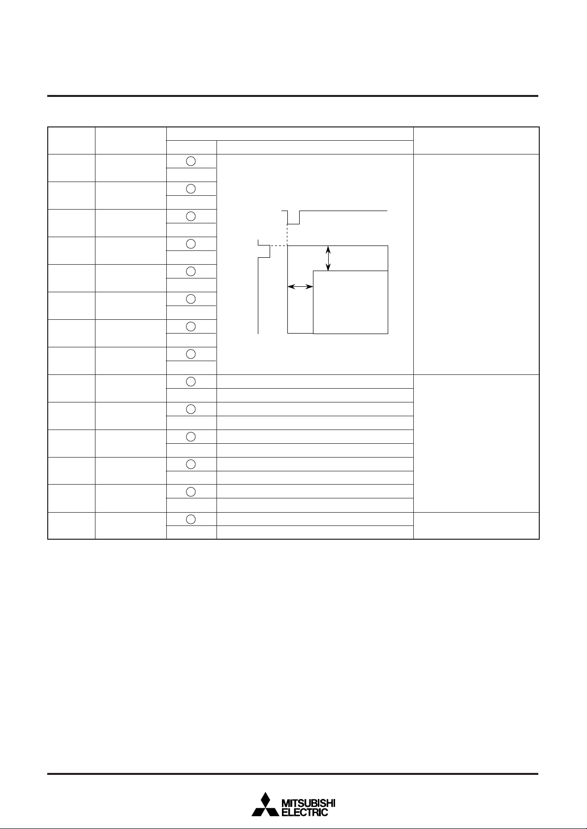
Display RAM DESCRIPTION
Display RAM Address 0016 to EF16
DA
0~C
0
1
2
3
4
5
6
7
8
9
A
B
C
Notes__1. Resetting at the AC pin RAM-erases the display RAM, and the status turns as indicated by the mark around in the status column.
2. Set to “1” only when setting a blank code. When using M35055-XXXFP, DA7 is C7 (MSB).
Name
C0
(LSB)
C1
C2
C3
C4
C5
C6
(MSB)
—
R
G
B
BLINK
REV
Status
0
1
0
1
0
1
0
1
0
1
0
1
0
1
0
1
0
1
0
1
0
1
0
1
0
1
Set ROM-held character code of a character needed
to display.
Set to “0” during normal operation
Can not be used
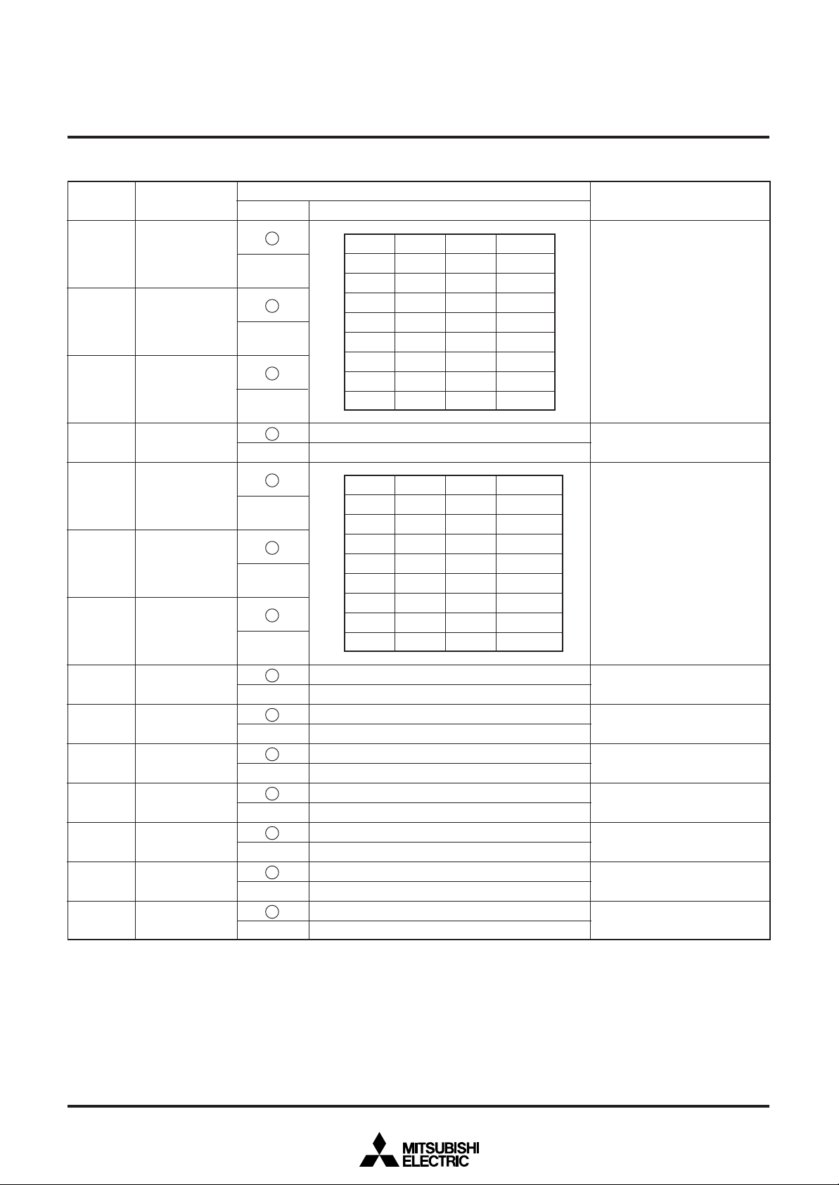
When RGBON=1, set background color by character
unit.
No blinking
Blinking
Normal character
Reversed character
Contents
Function
Remarks
(Note 2)
Refer to supplemental
explanation (3).
Refer to BLINK2 to 0
(address F516)
6
Display control register
(1) Address F016
DA
0~D
0
1
2
3
4
5
6
7
8
9
A
B
C
Register
PTC0
PTC1
PTD0
PTD1
SEPV0
SEPV1
SYSEP0
SYSEP1
TEST10
TEST11
TEST12
TEST13
TEST14
Status
0
1
0
1
0
1
0
1
0
1
0
1
0
1
0
1
0
1
0
1
0
1
0
1
0
1
MITSUBISHI MICROCOMPUTERS
M35054-XXXFP/M35055-XXXFP
SCREEN CHARACTER and PATTERN DISPLAY CONTROLLERS
Contents
Function
P0 output (port 0)
BLNK1 output
P1 output (port 1)
CO1 output
It is negative polarity at P0 output “L”, BLINK1 output.
It is positive polarity at P0 output “H”, BLINK1 output.
It is negative polarity at P01 output “L”, CO1 output.
It is positive polarity at P01 output “H”, CO1 output.
It should be fixed to “0”.
Can not be used.
It should be fixed to “0”.
Can not be used.
SYSEP1
0
0
1
1
It should be fixed to “0”.
Can not be used.
It should be fixed to “0”.
Can not be used.
Can not be used.
It should be fixed to “1”.
It should be fixed to “0”.
Can not be used.
It should be fixed to “0”.
Can not be used.
SYSEP0
0
1
0
1
Bias potential
Can not be used.
Can not be used.
1.75V
Can not be used.
Remarks
Port output control
Refer to supplemental explanation (4).
Control the port data
Refer to supplemental explanation (4).
Specifies the vertical synchronous
separation criterion
Refer to supplemental explanation (1).
Specifies the sync-bias potential
D
Note: The mark around the status value means the reset status by the “L” level is input to AC pin.
Notes
TEST15
0
1
It should be fixed to “0”.
Can not be used.
__
7
(2) Address F116
DA
0~D
0
1
2
3
4
5
6
7
8
9
A
B
C
D
Register
HP0
(LSB)
HP1
HP2
HP3
HP4
HP5
HP6
HP7
(MSB)
TEST16
TEST17
TEST18
TEST19
TEST20
TEST21
Status
0
1
0
1
0
1
0
1
0
1
0
1
0
1
0
1
0
1
0
1
0
1
0
1
0
1
0
1
M35054-XXXFP/M35055-XXXFP
SCREEN CHARACTER and PATTERN DISPLAY CONTROLLERS
Contents
Function
Let horizontal display start position be HS,
HS = T ✕ (Σ 2nHPn+6)
Can not be used.
It should be fixed to “1”.
Can not be used.
It should be fixed to “1”.
Can not be used.
It should be fixed to “1”.
Can not be used.
It should be fixed to “1”.
Can not be used.
It should be fixed to “1”.
It should be fixed to “0”.
Can not be used.
7
n=0
HOR
VS
VERT
HS
Character
displaying
area
T : The oscillation cycle of display clock
MITSUBISHI MICROCOMPUTERS
Remarks
Set the horizontal display start
position by use of HP7 through
HP0. HP7 to HP0 = (00000000)
to (00001111) setting is
forbidden.
It can be set this up to 240 steps
in increments of one T.
8
(3) Address F216
0~D
0
1
2
3
4
5
6
7
8
9
A
B
C
D
Register
VP0
(LSB)
VP1
VP2
VP3
VP4
VP5
VP6
VP7
(MSB)
TEST22
TEST23
TEST24
TEST25
TEST26
TEST27
Status
0
1
0
1
0
1
0
1
0
1
0
1
0
1
0
1
0
1
0
1
0
1
0
1
0
1
0
1
M35054-XXXFP/M35055-XXXFP
SCREEN CHARACTER and PATTERN DISPLAY CONTROLLERS
ContentsDA
Function
Let vertical display start position be VS,
VS = H ✕ Σ 2nVPnVS
Can not be used.
It should be fixed to “1”.
Can not be used.
It should be fixed to “1”.
Can not be used.
It should be fixed to “1”.
Can not be used.
It should be fixed to “1”.
Can not be used.
It should be fixed to “1”.
It should be fixed to “0”.
Can not be used.
7
n=0
HOR
VS
VERT
HS
Character
displaying
area
H : The oscillation cycle of horizontal
synchronous signal
MITSUBISHI MICROCOMPUTERS
Remarks
Set the vertical display start
position by use of VP7 through
VP0. VP7 to VP0 = (00000000)
to (00000110) setting is
forbidden.
It can be set this up to 249 steps
in increments of one H.
VP7 to VP0 = (00000000) to
(00100011) setting is forbidden.
9
(4) Address F316
0~D
0
1
2
3
4
5
6
7
8
9
A
B
C
D
Register
HSZ10
HSZ11
HSZ20
HSZ21
VSZ10
VSZ11
VSZ20
VSZ21
TEST28
TEST29
TEST30
TEST31
TEST32
TEST33
Status
0
1
0
1
0
1
0
1
0
1
0
1
0
1
0
1
0
1
0
1
0
1
0
1
0
1
0
1
SCREEN CHARACTER and PATTERN DISPLAY CONTROLLERS
ContentsDA
HSZ11
0
0
1
1
HSZ21
0
0
1
1
VSZ11
0
0
1
1
VSZ21
0
0
1
1
It should be fixed to “0”.
Can not be used.
It should be fixed to “0”.
Can not be used.
It should be fixed to “0”.
Can not be used.
It should be fixed to “0”.
Can not be used.
It should be fixed to “0”.
Can not be used.
It should be fixed to “0”.
Can not be used.
HSZ10
HSZ20
VSZ10
VSZ20
MITSUBISHI MICROCOMPUTERS
M35054-XXXFP/M35055-XXXFP
Function
0
1
0
1
0
1
0
1
0
1
0
1
0
1
0
1
Horizontal direction size
1T/dot
2T/dot
3T/dot
4T/dot
Horizontal direction size
1T/dot
2T/dot
3T/dot
4T/dot
Vertical direction size
1H/dot
2H/dot
3H/dot
4H/dot
Vertical direction size
1H/dot
2H/dot
3H/dot
4H/dot
Character size setting in the
horizontal direction for the first
line.
Character size setting in the
horizontal direction for the 2nd
line to 10th line.
Character size setting in the
vertical direction for the first line.
Character size setting in the
vertical direction for the 2nd line
to 10th line.
Remarks
10
(5) Address F416
0~D
0
1
2
3
4
5
6
7
8
9
A
B
C
D
Register
DSP0
DSP1
DSP2
DSP3
DSP4
DSP5
DSP6
DSP7
DSP8
DSP9
SPACE
TEST34
TEST35
TEST36
Status
0
1
0
1
0
1
0
1
0
1
0
1
0
1
0
1
0
1
0
1
0
1
0
1
0
1
0
1
M35054-XXXFP/M35055-XXXFP
SCREEN CHARACTER and PATTERN DISPLAY CONTROLLERS
ContentsDA
Function
BLK1
BLK0
0
0
1
1
Depends on BLK0 and BLK1 (address F816)
DSPn in the generic name for DSP0 to DSP9.
DSP0 to DSP9 are each controlled independently.
Normal display
Put a space line between line 2 and line 3, and
between line 8 and line 9.
It should be fixed to “0”.
Can not be used.
It should be fixed to “0”.
Can not be used.
It should be fixed to “0”.
Can not be used.
DSPn= “1”
Matrix-outline border
0
size
1
Border size
Matrix-outline size
0
1
Character size
DSPn= “0”
Matrix-outline size
Character size
Border size
Matrix-outline size
MITSUBISHI MICROCOMPUTERS
Remarks
Set the display mode of line 1.
Set the display mode of line 2.
Set the display mode of line 3.
Set the display mode of line 4.
Set the display mode of line 5.
Set the display mode of line 6.
Set the display mode of line 7.
Set the display mode of line 8.
Set the display mode of line 9.
Set the display mode of line 10.
Put a space line between line 2
and line 3 in displaying 32
characters.
11
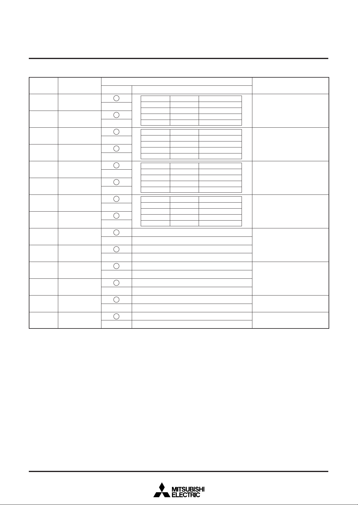
M35054-XXXFP/M35055-XXXFP
SCREEN CHARACTER and PATTERN DISPLAY CONTROLLERS
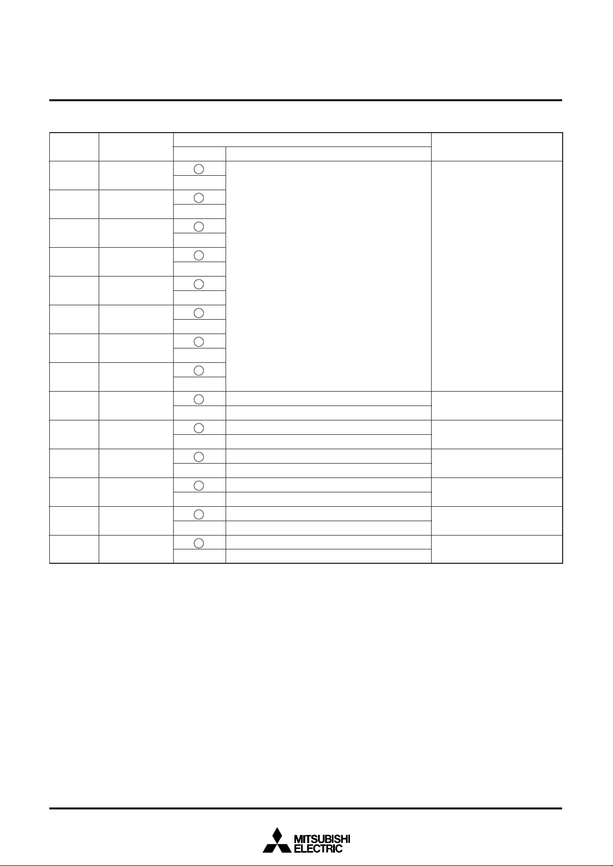
(6) Address F516
BLINK0
0
0
1
1
_
N/P
0
0
1
1
PALH
0
1
ContentsDA
Function
BLINK1
0
1
0
1
MPAL
0
1
0
1
__
INT/NON
0
1
0
1
0~D
0
Register
BLINK0
Status
0
1
1
BLINK1
0
1
0
2
BLINK2
1
_____
3
4
N/P
______________________
INT/NON
0
1
0
1
Division of vertical synchronizing signal into 1/64.
Cycle approximately 1 second.
Division of vertical synchronizing signal into 1/32.
Cycle approximately 0.5 second.
NTSC, M-PAL mode
PAL mode
Interlace
Non interlace
0
5
MPAL
1
0
6
PALH
1
7
EQP
0
1
8
TEST37
0
1
9
TEST38
0
1
A
TEST39
0
1
B
TEST40
0
1
C
TEST41
0
1
D
TEST42
0
1
Not include the equivalent pulse.
Include the equivalent pulse.
It should be fixed to “0”.
Can not be used.
It should be fixed to “0”.
Can not be used.
It should be fixed to “0”.
Can not be used.
It should be fixed to “0”.
Can not be used.
It should be fixed to “0”.
Can not be used.
It should be fixed to “0”.
Can not be used.
Note. To blink a character, set 1 to DAB (the blinking bit) of the display RAM.
MITSUBISHI MICROCOMPUTERS
Duty
Blinking off
25%
50%
75%
Synchronous mode
NTSC
M-PAL
PAL
Not available
Number of scanning lines
625H lines
626H lines
627H lines
628H lines
Remarks
Blinking duty ratio can be
altered. (Note)
Blinking cycle can be altered.
Refer to register MPAL
Scanning lines control (only in
internal synchronization)
Synchronizing signal is selected
with this register and N/P
_
register.
It should be fixed to “0” at NTSC
Effective only at non-interlace
12
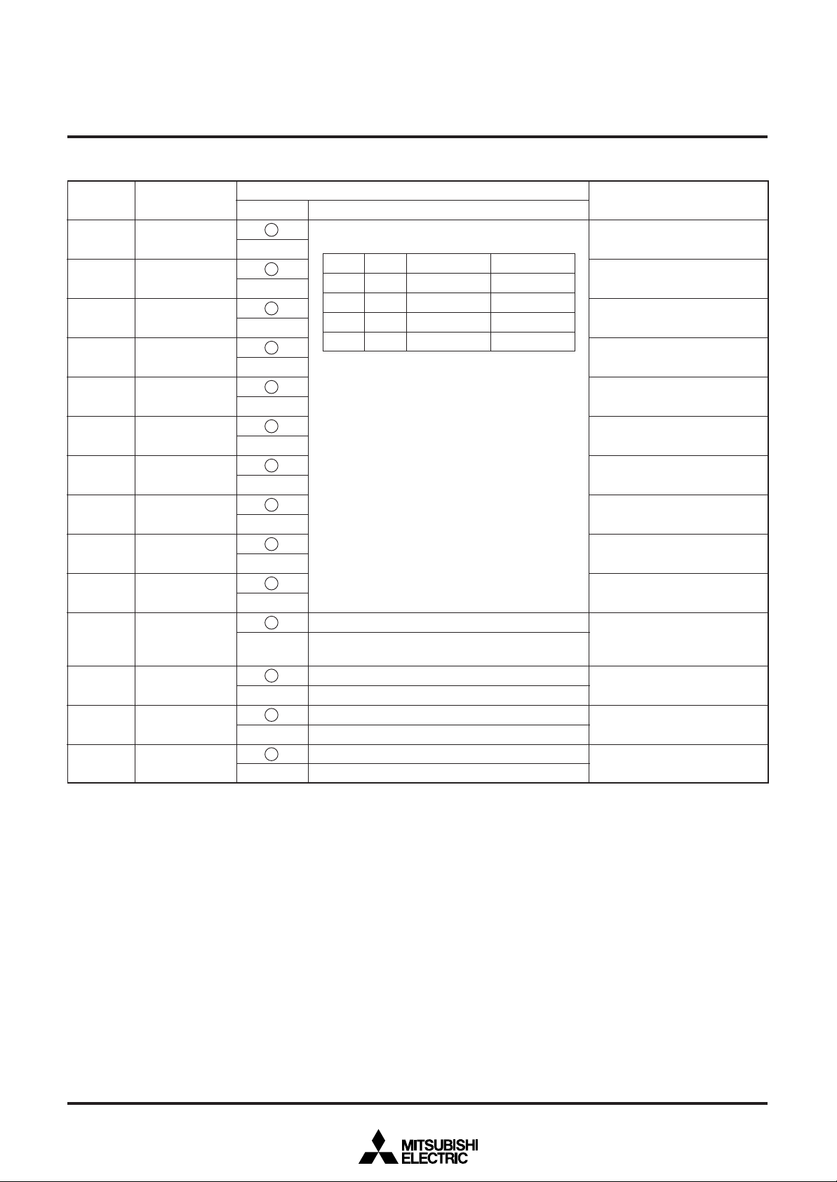
(7) Address F616
0~D
0
1
2
Register
PHASE0
PHASE1
PHASE2
Status
0
1
0
1
0
1
PHASE2
0
0
0
0
1
1
1
1
MITSUBISHI MICROCOMPUTERS
M35054-XXXFP/M35055-XXXFP
SCREEN CHARACTER and PATTERN DISPLAY CONTROLLERS
ContentsDA
PHASE1
0
0
1
1
0
0
1
1
Function
PHASE0
Raster
0
1
0
1
0
1
0
1
Black
Red
Green
Yellow
Blue
Magenta
Cyan
White
Raster color setting
Refer to supplemental
explanation (2) about video
signal level
Remarks
3
4
5
6
7
8
9
A
B
C
D
Note. It is neccessary to input the external composite video signal to the CVIN pin, and externally connect a 100 to 200Ω register in series.
LEVEL0
BR
BG
BB
BLKHF
__________
LIN24/32
LBLACK
TEST0
TEST1
TEST2
TEST43
0
1
0
1
0
1
0
1
0
1
0
1
0
1
0
1
0
1
0
1
0
1
Internal bias off
Internal bias on
BB
0
0
0
0
1
1
1
1
The halftone displaying “OFF” in superimpose
The halftone displaying “ON” in superimpose
24 characters ✕ 10 lines display
32 characters ✕ 7 lines display
Blanking level I 2.3V
Blanking level II 2.1V
It should be fixed to “0”.
Can not be used.
It should be fixed to “0”.
Can not be used.
It should be fixed to “0”.
Can not be used.
Can not be used.
It should to be fixed to “1”.
BG
0
0
1
1
0
0
1
1
BR
0
1
0
1
0
1
0
1
Character back-
ground color
Black
Red
Green
Yellow
Blue
Magenta
Cyan
White
Generates bias potential for
composite video signals
Character background color
setting.
Refer to supplemental
explanation (2) about video
signal level
This register is available in the
superimpose displaying only. (Note)
Set a blackness level
13
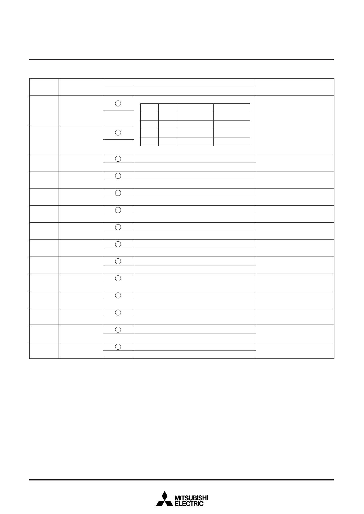
(8) Address F716
0~D
0
1
2
3
4
5
6
7
8
9
A
B
C
D
Register
CUR0
CUR1
CUR2
CUR3
CUR4
CUR5
CUR6
CUR7
CBLINK
__________
CL17/18
TEST44
RGBON
TEST45
TEST46
Status
0
1
0
1
0
1
0
1
0
1
0
1
0
1
0
1
0
1
0
1
0
1
0
1
0
1
0
1
MITSUBISHI MICROCOMPUTERS
M35054-XXXFP/M35055-XXXFP
SCREEN CHARACTER and PATTERN DISPLAY CONTROLLERS
ContentsDA
Function
Let cursor displaying address be CURS,
CURS = Σ 2nCURn
No blinking
Blinking
Cursor displaying at the 17th dot by vertical direction.
Cursor displaying at the 18th dot by vertical direction.
It should be fixed to “0”.
Can not be used.
Normal
Character background coloring
It should be fixed to “0”.
Can not be used.
It should be fixed to “0”.
Can not be used.
7
n=0
Remarks
Set the cursor displaying
address by use of CUR7 through
CUR0.
CUR7 to CUR0 (11110000)
setting is forbidden under 24
characters display.
CUR7 to CUR0 (11100000)
setting is forbidden under 32
characters display.
Set CUR7 to CUR0 = (11111111)
under cursor is not be displayed.
The cursor displaying address
(CURS) is correspond to display
construction.
The cursor blinking setting
Refer to character construction.
Refer to supplemental
explanation (3).
14
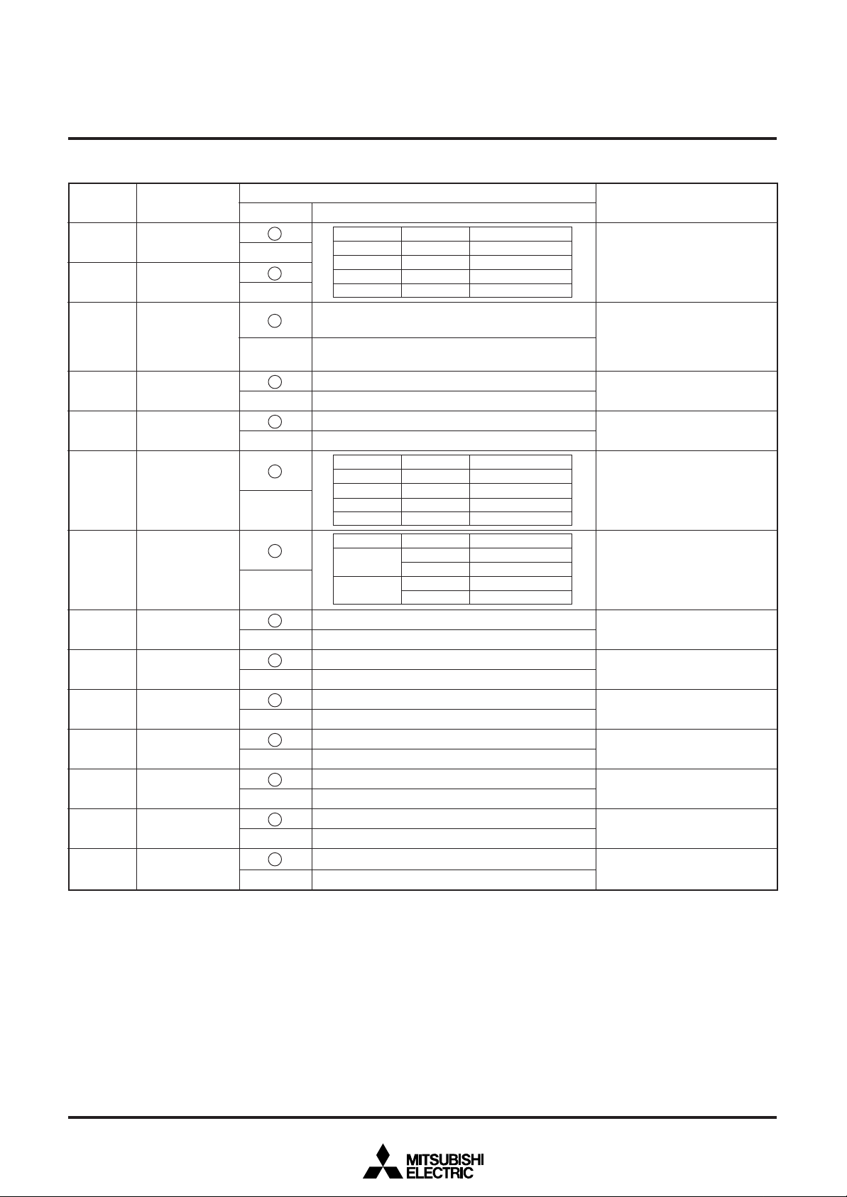
(9) Address F816
0~D
0
1
Register
BLK0
BLK1
Status
0
1
0
1
BLK1
0
0
1
1
MITSUBISHI MICROCOMPUTERS
M35054-XXXFP/M35055-XXXFP
SCREEN CHARACTER and PATTERN DISPLAY CONTROLLERS
ContentsDA
BLK0
0
1
0
Matrix-outline size
1
Function
DSPn= “1”
Matrix-outline
border size
Border size
Character size
DSPn= “0”
Matrix-outline size
Character size
Border size
Matrix-outline size
Display mode
(BLNK output) variable
Remarks
2
3
4
5
6
7
8
9
A
B
C
D
Notes 1. In dealing with the internal synchronization, cut off external video signals outside the IC. The leakage of external input video signals
can be avoided.
Notes 2. In displaying color superimposition, enter into the OSCIN pin the fSC signal that phase-synchronizes with the color burst of the
composite video signals (input to the CVIN pin).
Notes 3. Erases all the display RAM. The character code turns to blank-FF16, the encode data bit and the blinking bit turn to “1” respectively,
and reversed character bit turns to “0”.
EX
SCOR
STOPIN
STOP1
DSPON
RAMERS
TEST47
TEST48
TEST49
TEST50
TEST51
LEVEL1
0
1
0
1
0
1
0
1
0
1
0
1
0
1
0
1
0
1
0
1
0
1
0
1
External synchronization
Internal synchronization
Superimpose monotone display
Superimpose coloring display (only NTSC)
fSC input mode
Can not be used.
Oscillation VCO for display
Stop oscillation VCO for display
Display OFF
Display ON
RAM not erased
RAM erased
Can not be used.
It should be fixed to “1”.
Can not be used.
It should be fixed to “1”.
Can not be used.
It should be fixed to “1”.
Can not be used.
It should be fixed to “1”.
Can not be used.
It should be fixed to “1”.
Internal bias OFF
Internal bias ON
Synchronizing signal switching
(Note1)
“1” setting is forbidden at internal
synchronous or PAL, M-PAL
mode displaying.
OSCIN oscillation control
Control oscillation VCO for
display
This register does not exist
(Note 3).
Generates bias potential for synchronous separation.
15
MITSUBISHI MICROCOMPUTERS
M35054-XXXFP/M35055-XXXFP
SCREEN CHARACTER and PATTERN DISPLAY CONTROLLERS
Supplemental explanation about display control register
(1) How to effect synchronous separation from composite video signals
Synchronous separation is effected as follows depending on the width of L-level of the vertical synchronous period.
1. Less than 8.4µs ······ Not to be determined to be a vertical synchronous signal.
2. Equal to or higher than 8.4µs but less than 15.6µs ······ When two clocks continue, if take place, it is “L” period is determined to be a
vertical synchronization signal.
3. Equal to or higher than 15.6µs ······ It is “L” period is determined to be a vertical synchronous signal with no condition.
The determination is made at the timing indicated by V in Fig.4 either in case 2 or in case 3.
Sequence of synchronizing pulse
Composite video signal
8.4µs
Equalizing pulse
15.6
µ
s
Vertical synchronous signal
Fig. 5 The method of synchronous separation from composite video signal.
V8.4µs
16

Color
Sync-chip
Pedestal
Color burst
Black
Red
Green
Yellow
Blue
Magenta
Cyan
White
Phase angle (rad) Brightness level (V) Amplitude ratio (to color burst)
NTSC method
—
—
0
—
/16 ± 2 /16
7
27 16 ± 2 /16
/16 ± 2 /16
/16 ± 2 /16
17
/16 ± 2 /16
11
/16 ± 2 /16
23
—
SCREEN CHARACTER and PATTERN DISPLAY CONTROLLERS
PAL, M-PAL method
—
—
/16
± 4
—
± 7 /16 ± 2 /16
±
5 /16 ± 2 /16
/16 ± 2 /16
±
±
15 /16 ± 2 /16
/16 ± 2 /16
± 11
±
9 /16 ± 2 /16
—
MITSUBISHI MICROCOMPUTERS
M35054-XXXFP/M35055-XXXFP
VDD : 5.0V, Ta : 25°C(2) Video signal level
Min.
1.3
1.9
1.9
2.1
2.3
2.7
3.1
2.0
2.5
2.9
3.1
Typ.
1.5
2.1
2.1
2.3
2.5
2.9
3.3
2.2
2.7
3.1
3.3
Max.
1.7
2.3
2.3
2.5
2.7
3.1
3.5
2.4
2.9
3.3
3.5
Min.
—
—
—
—
1.5
1.4
1.0
1.0
1.4
1.5
—
Typ.
—
—
1.0
—
3.0
2.8
2.0
2.0
2.8
3.0
—
Max.
—
—
—
—
4.5
4.2
3.0
3.0
4.2
4.5
—
R-Y
CB1
RS1
/ 4
CB
-
/ 4
CB2
Fig. 6 Bector phases
(3) Setting RGBON (address F7
RGBON = “0” ..... Sets background colors depending on BB, BG,
and BR (address F616), screen by screen.
RGBON = “1”..... Sets background colors depending on R, G, B
(address 0016 to EF16), character by character.
The color setting is shown below.
RS2
16)
B-Y
CB Color burst under NTSC
CB1,CB2
RS1,RS2
Color Setting
Color burst under PAL or M-PAL
Color subcarrier under PAL or M-PAL
B
0
0
0
0
1
1
1
1
G
0
0
1
1
0
0
1
1
R
0
1
0
1
0
1
0
1
Color
Black
Red
Green
Y ellow
Blue
Magenta
Cyan
White
17

(4) Port output and BLNK1, CO1 output
MITSUBISHI MICROCOMPUTERS
M35054-XXXFP/M35055-XXXFP
SCREEN CHARACTER and PATTERN DISPLAY CONTROLLERS
BLNK1 (CO1)
PTD0 (PTD1)
1
PTC0 (PTC1)
0
Polarity switching
PTD0 (PTD1)
PTD0, 1, PTC0, 1 (Address F0
Fig. 7 Example of port control
(5) Setting conditions for oscillating or stopping the display clock
STOP1
DSPON
CS pin
at display clock operating
0
1
L
STOP1, CDSPON (Address F816)
at display clock stop
1
0
H
1
Output
0
Select
16)
(6) Setting condition at LEVEL0,1
Operation state (Character display)
External synchronous
LEVEL0 (address F616), LEVEL1 (address F816)
LEVEL0
LEVEL1
Internal synchronous
1
0
Now-working condition
(no characters are
displayed)
1
1
0
0
18

MITSUBISHI MICROCOMPUTERS
M35054-XXXFP/M35055-XXXFP
SCREEN CHARACTER and PATTERN DISPLAY CONTROLLERS
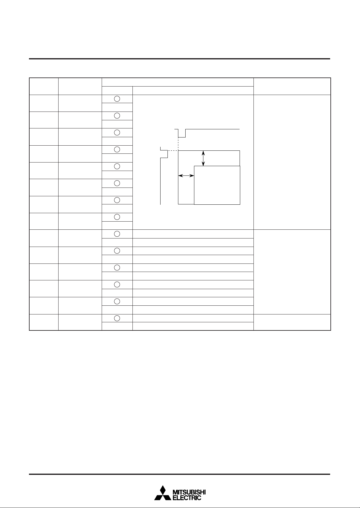
DISPLAY FORMS
M35054-XXXFP/M35055-XXXFP have the following four display
forms as the blanking function, when CO1 and BLNK1 are output.
(1) Character size : Blanking same as the character size.
(2) Border size : Blanking the background as a size from cha-
racter.
(3) Matrix-outline size: Blanking the background as a size from all
character font size.
(4) Matrix-outline : Blanking the background as a size from all
border size character font size.
Border display.
12 dots
Scanning
line
18 dots
12 dots
This display format allows each line to be controlled independently,
so that two kinds of display formats can be combined on the same
screen.
14 dots
14 dots
✽
CO1
BLNK1
✽
CVIDEO
aa
(1) Character size
Note: In this case, the output polarity that CO1 and BLNK1 is positive.
Fig. 8 Display forms at each display mode
aa
(2) Border size (3) Matrix-outline size
✽
✽
(4) Matrix-outline border size
a: Background carrier
color signal
19

SCREEN CHARACTER and PATTERN DISPLAY CONTROLLERS
DATA INPUT EXAMPLE
Data of display RAM and display control registers can be set by then
serial input function.
Owing to automatic address increment, not necessary to enter addresses for the second and subsequent data.
In automatically, the next of address F816 is assigned to address
0016.
Fig. 9 shows an example of data setting by the serial input function
(M35054-XXXFP), Fig. 10 shows an example of data setting by the
serial input function (M35055-XXXFP).
MITSUBISHI MICROCOMPUTERS
M35054-XXXFP/M35055-XXXFP
NO.
1 Address(F8
2
3
4
Data contewts
Address/Data
Data(F816)
Data(00
Data(01
16
16
Spplemental explanation
Address setting
16
)
Display OFF
)
)
Display RAM
address 00
to EF
16
setting
241
Data(EE16)
Data(EF
242
243
Data(F0
244
Data(F116)
245
Data(F2
246
Data(F3
247
Data(F4
248
Data(F5
249
Data(F6
250
Data(F7
251
Data(F8
Fig. 9 Example of data setting by the serial input function (M35054-XXXFP)
16
)
16
)
16
)
16
)
16
)
16
)
16
)
16
)
16
)
Register
address F0
to F7
16
setting
Display ON
DA DA DA
FE D
0
00 0
00 0
00 0
16
000
000
00 0
16
00 0
00 0
00 0
00 0
00 0
00 1
00 0
00
00
LEVEL
1
DA DA DA DA DA DA DA DA DA DA DA DA DA
CBA98 7654 32 1 0
000
000
BLINK
BLINK
REV
BLINK
REV
BLINK
REV
01
0
00
0
0
SPACE
0
0000
TESTTESTTEST
RGBON
00
0 011111000
0000000000
GRREV
BG R
BG R
BG R
0
DSP DSP DSP DSP DSP DSP DSP
LBLACK
012
CL
17/18
1
C6 C5 C4 C3 C2 C0C1B
0
C6 C5 C4 C3 C2 C0C1
0
C6 C5 C4 C3 C2 C0C1
0
C6 C5 C4 C3 C2 C0C1
0
PTD
000100
1
HP HP HP HP HP
11111
VP VP VP VP VP VP VP VP
11111
VSZ VSZ VSZ VSZ HSZ
00
CURSCURSCURSCURSCURSCURSCURS
STOP
1
INT
/NON
STOP
IN
N/P
LEVEL
0
SCOR
LIN
24/32
CBLINK
1111
EQP
BLKHF
RAM
ERS
PALH MPAL
BB BG BR
CURS
DSPON
PTD
0
HP
HSZ
DSP
BLINK
PHASE
EX
PTC
PTC
0
1
HP
HP
01234567
01234567
HSZ
HSZ
1011202110112021
DSP
DSP
0123456789
BLINK
BLINK
012
PHASE PHASE
012
01234567
BLK
BLK
0
1
20

MITSUBISHI MICROCOMPUTERS
M35054-XXXFP/M35055-XXXFP
SCREEN CHARACTER and PATTERN DISPLAY CONTROLLERS
NO.
Address(F8
1
2
3
4
Data couteuts
Address/Data
Data(F816)
Data(00
Data(01
16
16
Supplemental explauation
16
)
Address setting
Display OFF
)
)
Display RAM
address 00
to EF
16
setting
241
Data(EE16)
Data(EF
242
Data(F0
243
244
Data(F116)
245
Data(F2
Data(F3
246
247
Data(F4
248
Data(F5
249
Data(F6
250
Data(F7
Data(F8
251
Fig. 10 Example of data setting by the serial input function (M35055-XXXFP)
16
)
16
)
16
)
16
)
16
)
16
)
16
)
16
)
16
)
Register
address F0
to F7
16
setting
Display ON
DA DA DA
FE D
0
00 0
00 0
00 0
16
00
000
00 0
16
00 0
00 0
00 0
00 0
00 0
00 1
00 0
00
00
LEVEL
1
DA DA DA DA DA DA DA DA DA DA DA DA DA
C
BA98 7654 32 1 0
000
000
BLINK
BLINK
REV
BLINK
REV
BLINK
REV
01
0
00
SPACE
0
0
0
0000
TESTTEST TEST
RGBON
00
0 011111000
0000000000
GRREV
BG R
BG R
BG R
0
DSP DSP DSP DSP DSP DSP DSP
LBLACK
012
CL
17/18
1
C6 C5 C4 C3 C2 C0C1B
C7
C6 C5 C4 C3 C2 C0C1
C7
C6 C5 C4 C3 C2 C0C1
C7
C6 C5 C4 C3 C2 C0C1
C7
PTD
000100
1
HP HP HP HP HP
11111
VP VP VP VP VP VP VP VP
11111
VSZ VSZ VSZ VSZ HSZ
00
INT
N/P
/NON
LEVEL
0
CURSCURSCURSCURSCURSCURS
STOP
STOP
SCOR
IN
1
LIN
24/32
CBLINK
1111
EQP
BLKHF
CURS
RAM
ERS
PALH MPAL
BB BG BR
CURS
DSPON
PTD
0
HP
HSZ
DSP
BLINK
PHASE
EX
PTC
PTC
0
1
HP
HP
01234567
01234567
HSZ
HSZ
1011202110112021
DSP
DSP
0123456789
BLINK
BLINK
012
PHASE PHASE
012
01234567
BLK
BLK
01
21

SCREEN CHARACTER and PATTERN DISPLAY CONTROLLERS
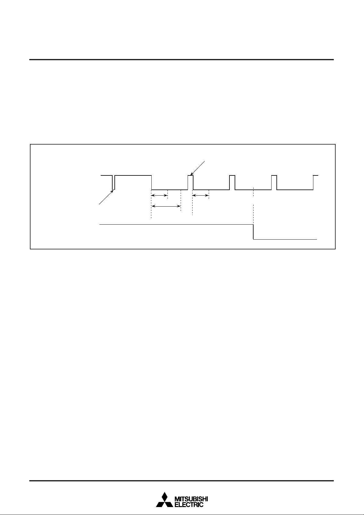
SERIAL DATA INPUT TIMING
(1)The address consists of 16 bits.
(2)The data consists of 16 bits.
(3)__The 16 bits in the SCK after the CS signal has fallen are the ad-
dress, and for succeeding input data, the address is incremented
every 16 bits.
CS
SCK
MITSUBISHI MICROCOMPUTERS
M35054-XXXFP/M35055-XXXFP
SIN
Fig. 11 Serial input timing
LSB MSB
Address (16 bit)
LSB MSB LSB MSB
Data N (16 bit)
Data N+1 (16 bit)
N =1, 2, 3
22

SCREEN CHARACTER and PATTERN DISPLAY CONTROLLERS
CHARACTER FONT
Images are composed on a 12 ✕ 18 dot matrix, and characters can
be linked vertically and horizontally with other characters to allow the
display the continuous symbols.
(1) Border display (set by register BLK0, 1 (address F816))
12 dots
MITSUBISHI MICROCOMPUTERS
M35054-XXXFP/M35055-XXXFP
Character code “FF16” is so fixed as to be blank and to have no
background, thus cannot assign a character font to this code.
When the character extends to the
top dot of the matrix, no border is
left at the top.
18 dots
(2) Cursor display (Border display)
Character
When the character extends to
the bottom (18th) dot of the matrix,
no border is left at the bottom.
Note: Hatching represents border.
Note: When the cursor positioning
at the bottom (18th) dot, no
border is left at the bottom.
Register CL17/18 (address F7
Fig. 12 Character font and border
Positioning the
cursor at the
17th dot.
“0”
)
=
16
Positioning the
cursor at the
18th dot.
Register CL17/18 =“0”
23

M35054-XXXFP/M35055-XXXFP
Note 7: In dealing with the internal synchronization,
cut off external video signals outside the IC.
The leakage of external input video signals
can be avoided.
Note 1: Clamp sync chip to 1.50V.
Note 2: Set basic electric potential in consid
eration of dynamic range of the tran-
sistor.
Note 3: External loop filter 1 constant is pro-
visional valve.
Note 4: Construct integral circuit by built-in 30kΩ
of AC pin and an external condenser.
Attention to supply voltage rise time about
this CR constant.
Note 5: External loop filter 2 constant is provi-
sional valve.
Note 6: Connect f
SC
frequency.
0.3Vp-p
4.0Vp-p
NTSC = 3.580MHz
PAL= 4.434MHz
M-PAL= 3.576MHz
220
2.2k
120
150
+7.0V
Composite video
signal input
10k
47µ
From microcomputer
+
Note 1
+5.0V
470
+7.0V
External composite video signal input
47 µ
Note 2
1.50V
75
220µ
+
Note 5
47P
Note 6
+
1
2
3
4
5
6
7
8
9
10
11
12
13
14
15
16
20
19
18
17
CP1
TESTA
SIN
CVIDEO
LECHA
CVIN
SCK
V
DD
2
CS
AC
V
DD
1
V
SS
HOR
P1
P0
OSCIN
TESTB
CP2
TESTC
1µ
+
1µ
100µ
0.01µ
+5.0V
+
+
Note 4
1k
0.01µ
0.22µ
470P
1.5k
fsc
Note 3
+5.0V
0.1µ
1µ
100µ
+
+
V
SS
Note 7
Delay
circuit
In displaying color superimposition, enter
into the OSCIN pin the f
SC
signal that
phase-synchronizes with the color burst of
the composite video signals (input to the
CVIN pin).
V
OSCIN
SCREEN CHARACTER and PATTERN DISPLAY CONTROLLERS
M35054-XXXFP/M35055-XXXFP PERIPHERAL CIRCUIT
MITSUBISHI MICROCOMPUTERS
Fig. 13 M35054-XXXFP/M35055-XXXFP example of peripheral circuit
24

Precautions
(1) Points to note in setting the display RAMs
a) Be careful to the edges may sway depending on the combina-
tion of character’s background color and raster color.
MITSUBISHI MICROCOMPUTERS
M35054-XXXFP/M35055-XXXFP
SCREEN CHARACTER and PATTERN DISPLAY CONTROLLERS
Edge sway
Fig. 14 Example of display
b) If what display exceeds the display area in dealing with exter-
nal synchronization, (if use double - size characters), set the
character code of the addresses lying outside that display area
blank code – “FF16”.
Inside of display
0016
1816
3016
4816
Outside of display area
0C16
0B16
2416
2316
4716
5F16
1716
2F16
Inside of display
Outside of
display area
Fig. 15 Example of display
C016
D816
Set blank code “FF
D716
EF16
” to character code of
16
Numbers are adresses
part.
25

MITSUBISHI MICROCOMPUTERS
M35054-XXXFP/M35055-XXXFP
SCREEN CHARACTER and PATTERN DISPLAY CONTROLLERS
(2) Before setting registers at the starting of system, be sure to reset
the M35052-XXXSP/FP by applying “L” level to the AC pin.
(3) Power supply noise
When power supply noise is generated, the internal oscillator circuit does not stabilize, whereby causing horizontal jitters across
the picture display. Therefore, connect a bypass capacitor between the power supply and GND.
(4) Synchronous correction action
When switching channel or in the special playback mode (quick
playback, rewinding, and so on) of VTR, effect of synchronous
correction becomes strong, and distortion of a character is apt to
occur because the continuity of video signal is suddenly switched.
When the continuity of video signal is out of order, erasure of
displayed characters is recommended in a extreme short time to
raise the quality of displayed characters.
(5) Notes on fSC signal input
This IC amplifies the subcarrier frequency (fSC) signal (NTSC, MPAL system: 3.58MHz, PAL system: 4.43MHz) input to the OSCIN
pin (17-pin) and generates the composite video signal internally.
The amplified fSC signal can be destabilized in the following cases.
a) When the fSC signal is outside of recommended operating con-
ditions.
b) When the waveform of the fSC signal is distorted.
c) When DC level in the fSC waveform fluctuates.
When the amplified signal is unstable, the composite video
signal generated inside the IC is also unstable in terms of syn-
chronization with the subcarrier and phase.
Consequently, this results in color flicker and lost synchroniza-
tion when the composite video signal is generated. Make note
of the fact that this may prevent a stable blue background from
being formed.
__
3) Wait 20 ms (the period necessary for the internal oscillation circuit to stabilize) before entering data.
4) Set necessary data in other registers, and make the display RAM
ready.
(6) Forbidding to stop entering the fSC signal
This IC doesn’t properly work if the fSC signal is not entered into
the OSCIN pin (pin 17), so don’t stop the fSC signal so as to work
the IC. To stop the IC, turn the display off (set 0 in the register
DSPON (address F816).)
(7) Forbidding to set data during the period in which the internal
oscillation circuit stabilizes
a) To start entering the fSC signal when its input is stopped.
b) To start oscillating the oscillation circuit for display when its
oscillation is stopped. (to assign “1” to the register STOP1 (address F816) when it is assigned “0”, or the like.)
c) To turn on the internal bias when it is turned off. (to assign “1”
to the register LEVEL1 (address F816) when it is assigned “0”.)
There can be instances in which data are not properly set in the
registers until the internal oscillation circuit stabilizes, so follow
the steps in sequence as given below.
1) Set “0” in the register DSPON (address F816). (the display is turned
off)
2) Effect the settings a), b), and c) given above.
26

MITSUBISHI MICROCOMPUTERS
M35054-XXXFP/M35055-XXXFP
SCREEN CHARACTER and PATTERN DISPLAY CONTROLLERS
TIMING REQUIREMENTS (Ta = –20°C to 70°C, VDD = 5±0.25V, unless otherwise noted)
Symbol
tw(SCK)
__
tsu(CS)
__
th(CS)
tsu(SIN)
th(SIN)
tword
SCK width
__
CS setup time
__
CS hold time
SIN setup time
SIN hold time
1 word writing time
Note. When oscillation stop at register STOR1 (address F816), 1V (field term) or more of tSU(CS) and th(CS) are needed.
CS
Parameter
Min.
400
200
200
200
12.8
__ __
tw(CS)
2µs
(min.)
2
Limits
Typ.
—
—
—
—
—
—
Max.
—
—
—
—
—
—
Unit
ns
ns
µ
ns
ns
µ
s
s
tsu(CS)
SCK
SIN
CS
SCK
12 1614 153 12 1614 153
Fig. 16 Serial input timing requirements
tw(SCK)
tsu(SIN) th(SIN)
tw(SCK)
tword
th(CS)
27

MITSUBISHI MICROCOMPUTERS
M35054-XXXFP/M35055-XXXFP
SCREEN CHARACTER and PATTERN DISPLAY CONTROLLERS
ABSOLUTE MAXIMUM RATINGS
V
DD
V
I
V
O
P
d
T
opr
T
stg
Symbol
Supply voltage
Input voltage
Output voltage
Power dissipation
Operating temperature
Storage temperature
Parameter
(VDD = 5V, Ta = –20 to 70°C, unless otherwise noted)
RECOMMENDED OPERATING CONDITIONS
Symbol
DD
V
V
IH
V
IL
V
CVIN
V
OSCIN
f
OSCIN
f
OSC1
f
OSC2
Supply voltage
“H”level input voltage AC, CS, SIN, SCK, TESTA, TESTB
________ _______
___________________
“L” level input voltage AC, CS, SIN, SCK, TESTA, TESTB
CVIN, HOR
Input voltage OSCIN (Note)
Synchronous signal oscillation frequency
Display oscillation frequency
Notes 1. Noise component is within 30mV.
Notes 2. f
H
: Horizontal synchronous frequency (MHz).
Parameter
Conditions
With respect to V
SS
Ratings
–0.3~6.0
SS
–0.3≤VI≤VDD+0.3
V
VSS≤VO≤V
Ta=25°C
300
–20~70
–40~125
(VDD = 5V, Ta = –20 to 70°C, unless otherwise noted)
Limits
Min.
4.75
0.8✕V
0
–
0.3V
P-P
DD
Typ.
5.00
V
2.0V
DD
0
P-P
–
3.580
(Duty 40~60%)
24 characters✕10 lines
32 characters✕7 lines
–
–
–
4.434
3.576
480✕f
640✕f
Unit
V
V
DD
V
mW
°C
°C
P-P
DD
Unit
V
V
V
V
V
MHz
MHz
MHz
Max.
5.25
V
DD
0.2✕V
–
4.0V
–
H
H
–
–
ELECTRICAL CHARACTERISTICS
V
DD
I
DD
V
OH
V
OL
R
I
Symbol
Supply voltage
Supply current
“H”level output voltage P0, P1
“L” level output voltage P0, P1
Pull-up resistance
__
__
AC, CS, SCK, SIN, TESTB
Parameter
(VDD = 5V, Ta = 25°C, unless otherwise noted)
VIDEO SIGNAL INPUT CONDITIONS
V
IN-SC
Symbol
Composite video signal input clamp voltage
Parameter
Test conditions
Ta=–20~70°C
V
DD
=5.00V
VDD=4.75V, IOH=–0.4mA
VDD=4.75V, IOL=0.4mA
DD
=5.00V
V
Min.
4.75
–
3.75
–
10
(VDD = 5V, Ta = –20 to 70°C, unless otherwise noted)
Test conditions
Sync-chip voltage
Min.
–
Limits
Typ.
5.00
30
–
–
30
Limits
Typ.
1.5
Max.
5.25
50
–
0.4
100
Max.
–
Unit
V
mA
V
V
kΩ
Unit
V
28

MITSUBISHI MICROCOMPUTERS
M35054-XXXFP/M35055-XXXFP
SCREEN CHARACTER and PATTERN DISPLAY CONTROLLERS
Note for Supplying Power
(1)__Timing of power supplying to AC pin
The internal circuit of M35054-XXXFP/ M35055-XXXFP is reset
when the level of the auto clear input pin AC is “L”. This pin is
hysteresis input with the pull-up resistor. The timing about power
supplying of AC pin is shown in Figure 16. tW is the interval after
the supply voltage becomes 0.8 ✕ VDD or more and before the
supply voltage to the AC pin (VAC) becomes 0.2 ✕ VDD or more.
After supplying the power (VDD and VSS) to M35054-XXXFP/
M35055-XXXFP, the tW time must be reserved for 1ms or more.
__
__
__
Voltage [V]
V
DD
DD
0.8✕V
__
Supply voltage
Before starting input from the microcomputer, the waiting time
(ts) must be reserved for 500ms after the supply voltage to the
__
AC pin becomes 0.8 ✕ VDD or more.
(2) Timing of power supplying to VDD1 pin and VDD2 pin
The power need to supply to VDD1 and VDD2 at a time, though it
is separated perfectly between the VDD1 as the digital line and
the VDD2 as the analog line.
V
AC
(AC pin input voltage)
DD
0.2✕V
w
t
Fig. 17 Timing of power supplying to AC pin
__
PRECAUTION FOR USE
Notes on noise and latch-up
Connect a capacitor (approx. 0.1 ˚F) between pins VDD and VSS at
the shortest distance using relatively thick wire to prevent noise and
latch up.
ts
Time t [s]
ROM ORDERING METHOD
Please submit the information described below when ordering Mask
ROM.
(1) ROM Order Confirmation Form .................................................1
(2) Data to be written into mask ROM ................................ EPROM
(three sets containing the identical data)
(3) Mark Specification Form............................................................1
(4) Program for character font generating + froppy disk in which char-
acter data is input
29

STANDARD ROM TYPE : M35054-001FP
M35054-001FP is a standard ROM type of M35054-XXXFP
character patterns are fixed to the contents of Figure 18 to 19.
MITSUBISHI MICROCOMPUTERS
M35054-XXXFP/M35055-XXXFP
SCREEN CHARACTER and PATTERN DISPLAY CONTROLLERS
30

MITSUBISHI MICROCOMPUTERS
M35054-XXXFP/M35055-XXXFP
SCREEN CHARACTER and PATTERN DISPLAY CONTROLLERS
0016 0116 0216 0316 0416 0516 0616 0716
0816 0916 0A16 0B16 0C16 0D16 0E16 0F16
13161116 1216 1416 1616 1716
1816 1916 1A16 1B16 1C16 1D16 1E16 1F16
2016 2116 2216 2316 2416 2516 2616 2716
2816 2916 2A16 2B16 2C16 2D16 2E16 2F16
15161016
3016 3116 3216 3316 3416 3516 3616 3716
3816 3916 3A16 3B16 3C16 3D16 3E16 3F16
Fig. 18 M35054-001FP character pattern (1)
31

MITSUBISHI MICROCOMPUTERS
M35054-XXXFP/M35055-XXXFP
SCREEN CHARACTER and PATTERN DISPLAY CONTROLLERS
4016 4116 4216 4316 4416 4516 4616 4716
4816 4916 4A16 4B16 4C16 4D16 4E16 4F16
5016 5116 5216 5316 5416 5516 5616 5716
5816 5916 5A16 5B16 5C16 5D16 5E16 5F16
6016 6116 6216 6316 6416 6516 6616 6716
6816 6916 6A16 6B16 6C16 6D16 6E16 6F16
7016 7116 7216 7316 7416 7516 7616 7716
7816 7916 7A16 7B16 7C16 7D16 7E16 7F16
Fig. 19 M35054-001FP character pattern (2)
32

STANDARD ROM TYPE : M35055-001FP
M35055-001FP is a standard ROM type of M35055-XXXFP
Character patterns are fixed to the contents of Figure 20 to 23.
MITSUBISHI MICROCOMPUTERS
M35054-XXXFP/M35055-XXXFP
SCREEN CHARACTER and PATTERN DISPLAY CONTROLLERS
33

MITSUBISHI MICROCOMPUTERS
M35054-XXXFP/M35055-XXXFP
SCREEN CHARACTER and PATTERN DISPLAY CONTROLLERS
0016 0116 0216 0316 0416 0516 0616 0716
0816 0916 0A16 0B16 0C16 0D16 0E16 0F16
1016 13161116 1216 1416 1516 1616 1716
1816 1916 1A16 1B16 1C16 1D16 1E16 1F16
2016 2116 2216 2316 2416 2516 2616 2716
2816 2916 2A16 2B16 2C16 2D16 2E16 2F16
3016 3116 3216 3316 3416 3516 3616 3716
3816 3916 3A16 3B16 3C16 3D16 3E16 3F16
Fig. 20 M35055-001FP character pattern (1)
34

MITSUBISHI MICROCOMPUTERS
M35054-XXXFP/M35055-XXXFP
SCREEN CHARACTER and PATTERN DISPLAY CONTROLLERS
4016 4116 4216 4316 4416 4516 4616 4716
4816 4916 4A16 4B16 4C16 4D16 4E16 4F16
5016 5116 5216 5316 5416 5516 5616 5716
5816 5916 5A16 5B16 5C16 5D16 5E16 5F16
6016 6116 6216 6316 6416 6516 6616 6716
6816 6916 6A16 6B16 6C16 6D16 6E16 6F16
7016 7116 7216 7316 7416 7516 7616 7716
7816 7916 7A16 7B16 7C16 7D16 7E16 7F16
Fig. 21 M35055-001FP character pattern (2)
35

MITSUBISHI MICROCOMPUTERS
M35054-XXXFP/M35055-XXXFP
SCREEN CHARACTER and PATTERN DISPLAY CONTROLLERS
8016 8116 8216 8316 8416 8516 8616 8716
8816 8916 8A16 8B16 8C16 8D16 8E16 8F16
9016 9116 9216 9316 9416 9516 9616 9716
9816 9916 9A16 9B16 9C16 9D16 9E16 9F16
A016 A116 A216 A316 A416 A516 A616 A716
A816 A916 AA16 AB16 AC16 AD16 AE16 AF16
B016 B116 B216 B316 B416 B516 B616 B716
B816 B916 BA16 BB16 BC16 BD16 BE16 BF16
Fig. 22 M35055-001FP character pattern (3)
36

MITSUBISHI MICROCOMPUTERS
M35054-XXXFP/M35055-XXXFP
SCREEN CHARACTER and PATTERN DISPLAY CONTROLLERS
C016 C116 C216 C316 C416 C516 C616 C716
C816 C916 CA16 CB16 CC16 CD16 CE16 CF16
D016 D116 D216 D316 D416 D516 D616 D716
D816 D916 DA16 DB16 DC16 DD16 DE16 DF16
E016 E116 E216 E316 E416 E516 E616 E716
E816 E916 EA16 EB16 EC16 ED16 EE16 EF16
F016 F116 F216 F316 F416 F516 F616 F716
F816 F916 FA16 FB16 FC16 FD16 FE16 FF16 blank
Fig. 23 M35055-001FP character pattern (4)
37

MASK ROM ORDER CONFIRMATION FORM
GZZ-SH00-59B <75A0>
MITSUBISHI MICROCOMPUTERS
M35054-XXXFP/M35055-XXXFP
SCREEN CHARACTER and PATTERN DISPLAY CONTROLLERS
Mask ROM number
MASK ROM ORDER CONFIRMATION FORM
SCREEN DISPLAY IC M35054-XXXFP
MITSUBISHI ELECTRIC
Note : Please fill in all items marked ❈, .
Company
❈
Customer
❈
Program version name M054R V
❈Remarks
● Return the Character Font Preparation Program after use.
● Three EPROMs are required. (All the three EPROMs must be same types. Check
(1) The font data prepared by the Character Font Preparation Program is saved as a binary type object file
(2) Attach the erase protect seals on three EPROMs. Each seal bears the type name (M35054), and ROM No.
● Write the checksum code (hexadecimal notation) for entire EPROM areas.
name
Data
issued
27512
(addresses 0000h to 7FFFh). Three sets of these EPROMs are required.
(–...FP).
Date :
TEL
()
Approval
Issuance
signature
✔ in the appropriate box.)
Section head
signature
Receipt
Data :
Verification
Supervisor
signature
Framing
Checksum
● Select the marking type (Check
Special Mark .......Fill in the Mark Specification Form (20P2Q-A for M35054-XXXFP) and attach to the
Mask ROM Order Confirmation Form.
Standard Mark
● The package type
❈●Comments
✔ in the appropriate box).
.......No writing is required.
....... SSOP type (M35054-XXXFP)
38

MITSUBISHI MICROCOMPUTERS
M35054-XXXFP/M35055-XXXFP
SCREEN CHARACTER and PATTERN DISPLAY CONTROLLERS
GZZ-SH00-59B <75A0>
❈
1.Test patterns
########
(The patterns with the mark “#” are test patterns)
❈
2.Character patterns (See the next page)
FF
16
blank
Mask ROM number
39

MITSUBISHI MICROCOMPUTERS
M35054-XXXFP/M35055-XXXFP
SCREEN CHARACTER and PATTERN DISPLAY CONTROLLERS
0016 0116 0216 0316 0416 0516 0616 0716
0816 0916 0A16 0B16 0C16 0D16 0E16 0F16
1016 1116 1216 1316 1416 1516 1616 1716
1816 1916 1A16 1B16 1C16 1D16 1E16 1F16
2016 2116 2216 2316 2416 2516 2616 2716
2816 2916 2A16 2B16 2C16 2D16 2E16 2F16
3016 3116 3216 3316 3416 3516 3616 3716
40
3816 3916 3A16 3B16 3C16 3D16 3E16 3F16

MITSUBISHI MICROCOMPUTERS
M35054-XXXFP/M35055-XXXFP
SCREEN CHARACTER and PATTERN DISPLAY CONTROLLERS
4016 4116 4216 4316 4416 4516 4616 4716
4816 4916 4A16 4B16 4C16 4D16 4E16 4F16
5016 5116 5216 5316 5416 5516 5616 5716
5816 5916 5A16 5B16 5C16 5D16 5E16 5F16
6016 6116 6216 6316 6416 6516 6616 6716
6816 6916 6A16 6B16 6C16 6D16 6E16 6F16
7016 7116 7216 7316 7416 7516 7616 7716
7816 7916 7A16 7B16 7C16 7D16 7E16 7F16
41

MASK ROM ORDER CONFIRMATION FORM
GZZ-SH00-60B <75A0>
MITSUBISHI MICROCOMPUTERS
M35054-XXXFP/M35055-XXXFP
SCREEN CHARACTER and PATTERN DISPLAY CONTROLLERS
Mask ROM number
MASK ROM ORDER CONFIRMATION FORM
SCREEN DISPLAY IC M35055-XXXFP
MITSUBISHI ELECTRIC
Note : Please fill in all items marked ❈, .
Company
❈
Customer
❈
Program version name M055R V
❈Remarks
● Return the Character Font Preparation Program after use.
● Three EPROMs are required. (All the three EPROMs must be same types. Check
(1) The font data prepared by the Character Font Preparation Program is saved as a binary type object file
(2) Attach the erase protect seals on three EPROMs. Each seal bears the type name (M35055), and ROM No.
● Write the checksum code (hexadecimal notation) for entire EPROM areas.
name
Data
issued
27512
(addresses 0000h to 7FFFh). Three sets of these EPROMs are required.
(–...FP).
Date :
TEL
()
Approval
Issuance
signature
✔ in the appropriate box.)
Section head
signature
Receipt
Data :
Verification
Supervisor
signature
Framing
Checksum
● Select the marking type (Check
Special Mark .......Fill in the Mark Specification Form (20P2Q-A for M35055-XXXFP) and attach to the
Mask ROM Order Confirmation Form.
Standard Mark
● The package type
❈●Comments
✔ in the appropriate box).
.......No writing is required.
....... SSOP type (M35055-XXXFP)
42

MITSUBISHI MICROCOMPUTERS
M35054-XXXFP/M35055-XXXFP
SCREEN CHARACTER and PATTERN DISPLAY CONTROLLERS
GZZ-SH00-60B <75A0>
❈1.Test patterns
#
(The patterns with the mark “#” are test patterns)
❈2.Character patterns (See the next page)
#######
Mask ROM number
43

MITSUBISHI MICROCOMPUTERS
M35054-XXXFP/M35055-XXXFP
SCREEN CHARACTER and PATTERN DISPLAY CONTROLLERS
0016 0116 0216 0316 0416 0516 0616 0716
0816 0916 0A16 0B16 0C16 0D16 0E16 0F16
1016 1116 1216 1316 1416 1516 1616 1716
1816 1916 1A16 1B16 1C16 1D16 1E16 1F16
2016 2116 2216 2316 2416 2516 2616 2716
2816 2916 2A16 2B16 2C16 2D16 2E16 2F16
3016 3116 3216 3316 3416 3516 3616 3716
44
3816 3916 3A16 3B16 3C16 3D16 3E16 3F16

MITSUBISHI MICROCOMPUTERS
M35054-XXXFP/M35055-XXXFP
SCREEN CHARACTER and PATTERN DISPLAY CONTROLLERS
4016 4116 4216 4316 4416 4516 4616 4716
4816 4916 4A16 4B16 4C16 4D16 4E16 4F16
5016 5116 5216 5316 5416 5516 5616 5716
5816 5916 5A16 5B16 5C16 5D16 5E16 5F16
6016 6116 6216 6316 6416 6516 6616 6716
6816 6916 6A16 6B16 6C16 6D16 6E16 6F16
7016 7116 7216 7316 7416 7516 7616 7716
7816 7916 7A16 7B16 7C16 7D16 7E16 7F16
45

MITSUBISHI MICROCOMPUTERS
M35054-XXXFP/M35055-XXXFP
SCREEN CHARACTER and PATTERN DISPLAY CONTROLLERS
8016 8116 8216 8316 8416 8516 8616 8716
8816 8916 8A16 8B16 8C16 8D16 8E16 8F16
9016 9116 9216 9316 9416 9516 9616 9716
9816 9916 9A16 9B16 9C16 9D16 9E16 9F16
A016 A116 A216 A316 A416 A516 A616 A716
A816 A916 AA16 AB16 AC16 AD16 AE16 AF16
B016 B116 B216 B316 B416 B516 B616 B716
46
B816 B916 BA16 BB16 BC16 BD16 BE16 BF16

MITSUBISHI MICROCOMPUTERS
M35054-XXXFP/M35055-XXXFP
SCREEN CHARACTER and PATTERN DISPLAY CONTROLLERS
C016 C116 C216 C316 C416 C516 C616 C716
C816 C916 CA 16 CB 16 CC 16 CD 16 CE 16 CF16
D016 D116 D216 D316 D416 D516 D616 D716
D816 D916 DA 16 DB 16 DC 16 DD 16 DE 16 DF16
E016 E116 E216 E316 E416 E516 E616 E716
E816 E916 EA 16 EB 16 EC 16 ED 16 EE16 EF16
F016 F116 F216 F316 F416 F516 F616 F716
F816 F916 FA16 FB16 FC16 FD 16 FE16 FF16 blank
47

MITSUBISHI MICROCOMPUTERS
M35054-XXXFP/M35055-XXXFP
SCREEN CHARACTER and PATTERN DISPLAY CONTROLLERS
20P2Q-A (20-PIN SSOP) MARK SPECIFICATION FORM
Mitsubishi IC catalog name
Please choose one of the marking types below (A, B, C), and enter the Mitsubishi IC catalog name and the special mark (if needed).
A. Standard Mitsubishi Mark
20
11
Mitsubishi IC catalog name
Mitsubishi lot number
(6-digit or 7-digit)
1
B. Customer s Parts Number + Mitsubishi IC Catalog Name
20
ROM number (3-digit)
Mitsubishi lot number (4-digit)
1
10
11
10
Mitsubishi IC catalog name
Customer s Parts Number
Note: The fonts and size of characters are standard Mitsubishi type.
Mitsubishi IC catalog name and Mitsubishi lot number
Notes1 : The mark field should be written right aligned.
2 : The fonts and size of characters are standard Mitsubishi
type.
3 : Customer s Parts Number can be up to 10 characters: Only
0 to 9, A to Z, +, -, /, (, ), &, ', . (period), and , (comma) are
usable.
4 : If the Mitsubishi logo is not required, check the box be-
low.
Mitsubishi logo is not required
C. Special Mark Required
20
1
48
11
10
Note 1 : If the Special Mark is to be Printed, indicate the desired
layout of the mark in the left figure. The layout will be duplicated as close as possible.
Mitsubishi lot number (4-digit) and Mask ROM
number (3-digit) are always marked.
2 : If the customer s trade mark logo must be used in the
Special Mark, check the box below.
Please submit a clean original of the logo.
For the new special character fonts, a clean font original
(ideally logo drawing) must be submitted.
Special logo required
Special Mark (Customer s Trade Mark)
Mitsubishi IC catalog name

PACKAGE OUTLINE
MITSUBISHI MICROCOMPUTERS
M35054-XXXFP/M35055-XXXFP
SCREEN CHARACTER and PATTERN DISPLAY CONTROLLERS
49

MITSUBISHI MICROCOMPUTERS
M35054-XXXFP/M35055-XXXFP
SCREEN CHARACTER and PATTERN DISPLAY CONTROLLERS
HEAD OFFICE: 2-2-3, MARUNOUCHI, CHIYODA-KU, TOKYO 100-8310, JAPAN
Keep safety first in your circuit designs!
• Mitsubishi Electric Corporation puts the maximum effort into making semiconductor products better and more reliable, but there is always the possibility that trouble may occur with them. Trouble with semiconductors may lead to
personal injury, fire or property damage. Remember to give due consideration to safety when making your circuit designs, with appropriate measures such as (i) placement of substitutive, auxiliary circuits, (ii) use of non-flammable
material or (iii) prevention against any malfunction or mishap.
Notes regarding these materials
• These materials are intended as a reference to assist our customers in the selection of the Mitsubishi semiconductor product best suited to the customer’s application; they do not convey any license under any intellectual property
rights, or any other rights, belonging to Mitsubishi Electric Corporation or a third party.
• Mitsubishi Electric Corporation assumes no responsibility for any damage, or infringement of any third-party’s rights, originating in the use of any product data, diagrams, charts, programs, algorithms, or circuit application examples
contained in these materials.
• All information contained in these materials, including product data, diagrams, charts, programs and algorithms represents information on products at the time of publication of these materials, and are subject to change by
Mitsubishi Electric Corporation without notice due to product improvements or other reasons. It is therefore recommended that customers contact Mitsubishi Electric Corporation or an authorized Mitsubishi Semiconductor product
distributor for the latest product information before purchasing a product listed herein.
The information described here may contain technical inaccuracies or typographical errors. Mitsubishi Electric Corporation assumes no responsibility for any damage, liability, or other loss rising from these inaccuracies or errors.
Please also pay attention to information published by Mitsubishi Electric Corporation by various means, including the Mitsubishi Semiconductor home page (http://www.mitsubishichips.com).
• When using any or all of the information contained in these materials, including product data, diagrams, charts, programs, and algorithms, please be sure to evaluate all information as a total system before making a final decision
on the applicability of the information and products. Mitsubishi Electric Corporation assumes no responsibility for any damage, liability or other loss resulting from the information contained herein.
• Mitsubishi Electric Corporation semiconductors are not designed or manufactured for use in a device or system that is used under circumstances in which human life is potentially at stake. Please contact Mitsubishi Electric
Corporation or an authorized Mitsubishi Semiconductor product distributor when considering the use of a product contained herein for any specific purposes, such as apparatus or systems for transportation, vehicular, medical,
aerospace, nuclear, or undersea repeater use.
• The prior written approval of Mitsubishi Electric Corporation is necessary to reprint or reproduce in whole or in part these materials.
• If these products or technologies are subject to the Japanese export control restrictions, they must be exported under a license from the Japanese government and cannot be imported into a country other than the approved
destination.
Any diversion or reexport contrary to the export control laws and regulations of Japan and/or the country of destination is prohibited.
• Please contact Mitsubishi Electric Corporation or an authorized Mitsubishi Semiconductor product distributor for further details on these materials or the products contained therein.
© 2000 MITSUBISHI ELECTRIC CORP.
New publication, effective July. 2000.
Specifications subject to change without notice.

REVISION DESCRIPTION LIST M35054-XXXFP/M35055-XXXFP DATA SHEET
Rev. Rev.
No. date
1.0 First Edition 980402
1.1 P48 20P2Q-A (20-PIN SSOP) MARK SPECIFICATION FORM 000707
B: Note 4 added
Revision Description
(1/1)
 Loading...