Mitsubishi M35053-XXXFP, M35053-XXXSP Datasheet
MITSUBISHI MICROCOMPUTERS
M35053-XXXSP/FP
SCREEN CHARACTER and PATTERN DISPLAY CONTROLLERS
DESCRIPTION
The M35053-XXXSP/FP is TV screen display control IC which can
be used to display information such as number of channels, the date
and messages and program schedules on the TV screen.
In particular, owing to the built-in SYNC-SEP (synchronous separation) circuit, the synchronous correction circuit, the Decoder circuit,
and to the Encoder circuit, external circuits can be decrease and
character turbulence that occurs when superimposing can be reduced.
The processor can conform to the EDS broadcast service and is suitable for AV systems such as VTRs, LDs, and so on.
It is a silicon gate CMOS process and M35053-XXXSP is housed in
a 20-pin shrink DIP package, M35053-XXXFP is housed in a 20-pin
shrink SOP package.
For M35053-001SP/FP that is a standard ROM version of M35053XXXSP/FP respectively, the character pattern is also mentioned.
FEATURES
Screen composition .............................. 24 characters ✕ 10 lines,
•
Number of characters displayed ..................................240 (Max.)
•
Character composition ..................................... 12 ✕ 18 dot matrix
•
Characters available ............................................. 256 characters
•
Character sizes available....................4 (horizontal) ✕ 4 (vertical)
•
Display locations available
•
Horizontal direction............................................... 240 locations
Vertical direction ................................................... 256 locations
Blinking .................................................................Character units
•
Cycle : approximately 1 second, or approximately 0.5 seconds
Duty : 25%, 50%, or 75%
Data input..............................By the serial input function (16 bits)
•
Coloring
•
Background coloring (composite video signal)
Blanking
•
Total blanking (14 ✕ 18 dots)
Border size blanking
Character size blanking
Synchronizing signal
•
Composite synchronizing signal generation
(PAL, NTSC, M-PAL)
2 output ports (1 digital line)
•
Oscillation stop function
•
It is possible to stop the oscillation for synchronizing signal
generation
Built-in half-tone display function
•
Built-in reversed character display function
•
Built-in Decoder (NTSC only)
•
Built-in Encoder (NTSC only)
•
Built-in synchronous correction circuit
•
Built-in synchronous separation circuit
•
32 characters ✕ 7 lines
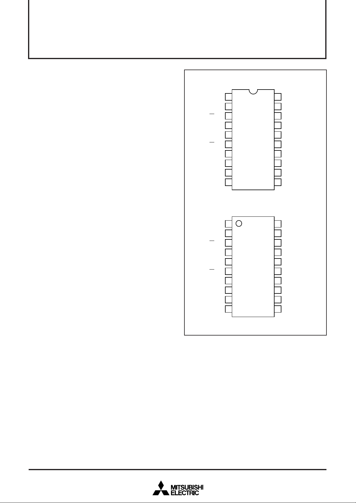
PIN CONFIGURATION (TOP VIEW)
CP1
TESTA
CS
SCK
SIN
AC
V
DD2
CVIDEO
LECHA
CVIN
CP1
TESTA
CS
SCK
SIN
AC
V
DD2
CVIDEO
LECHA
CVIN
1
←
2
3
→
4
→
5
↔
6
→
7
8
←
9
→
10
→
Outline 20P4B
1
←
2
3
→
4
→
5
↔
6
→
7
8
←
9
→
10
→
Outline 20P2Q-A
M35053-XXXSP
M35053-XXXFP
20
19
←
18
→
17
←
16
15
→
14
→
13
12
→
11
20
19
←
18
→
17
←
16
15
→
14
→
13
12
→
11
DD1
V
HOR
CP2
OSCIN
V
SS
P1
P0
TESTB
EDO
V
SS
DD1
V
HOR
CP2
OSCIN
V
SS
P1
P0
TESTB
EDO
V
SS
APPLICATION
TV, VCR, Movie
REV.1.1

PIN DESCRIPTION
Symbol
OSC1
TESTA
__
CS
SCK
SIN
__
AC
VDD2
CVIDEO
LECHA
CVIN
VSS
EDO
TESTB
P0
P1
VSS
OSCIN
CP2
HOR
VDD1
Pin name
Clock input
Test pin
Chip select input
Serial clock input
Serial data input/
output
Auto-clear input
Power pin
Composite video
signal output
Character level input
Composite video
signal input
Earthing pin
Encode data output
Test pin
Port P0 output
Port P1 output
Earthing pin
fSC input pin for
synchronous signal
generation
Filter output
Horizontal synchro-
nizing signal input
Power pin
Input/
Output
Input
—
Input
Input
Input/
Output
Input
—
Output
Input
Input
—
Output
—
Output
Output
—
Input
Output
Input
—
MITSUBISHI MICROCOMPUTERS
M35053-XXXSP/FP
SCREEN CHARACTER and PATTERN DISPLAY CONTROLLERS
Function
This is the filter output pin 1.
This is the pin for test. Connect this pin to GND during normal operation.
This is the chip select pin, and when serial data transmission is being carried out, it goes
to “L”. Hysteresis input. Includes built-in pull-up resistor.
__
When CS pin is “L”, SIN serial data is taken in when SCK rises. Hysteresis input. Built-in
pull-up resistor is included.
This is the pin for serial input of data and addresses for the display control register and
the display data memory. Also, serially outputs decode data according to the settings in
the relevant registers (serial I/O).
When “L”, this pin resets the internal IC circuit. Hysteresis input. Includes built-in pull-up
resistor.
Please connect to +5V with the analog circuit power pin.
This is the output pin for composite video signals. It outputs 2VP-P composite video
signals. In superimpose mode, character output etc. is superimposed on the external
composite video signals from CVIN.
This is the input pin which determines the “white” character color level in the composite
video signal.
This is the input pin for external composite video signals. In superimpose mode, character
output etc. is superimposed on these external composite video signals.
Please connect to GND using circuit earthing pin.
This is the output pin for encode data. It outputs digital three-value data or composite video signals.
This is the pin for test. Connect this pin to GND during normal operation.
This pin outputs the port output or BLNK1 (character background) signal.
This pin outputs the port output or CO1(character) signal.
Please connect to GND using circuit earthing pin (Analog side).
This is the input pin for the sub-carrier frequency (fSC) for generating a synchronous
signal.
A frequency of 3.580MHz is needed for NTSC, and a frequency of 4.434MHz in needed
for PAL and 3.576MHz is needed for M-PAL.
Filter output pin 2.
This is the input pin for external composite video signals. This pin inputs the external
video signal clamped sync-chip to 1.5V, and internally carries out synchronous separation.
Please connect to +5V with the digital circuit power pin.
2
MITSUBISHI MICROCOMPUTERS
Data
control
circuit
Address
control
circuit
Display control
register
Display RAM
Display character ROM
Timing
generator
Blinking circuit
Shift register
Display control
circuit
Reading address
control circuit
H counter
NTSC
PAL
M-PAL
video output
circuit
Timing
generator
SYNC-SEP
circuit
3.580MHz(NTSC)
4.434MHz(PAL)
3.576MHz(M-PAL)
TESTA
TESTB
Port output
circuit
Decoder circuit
Clock oscillation circuit
Data slicer
circuit
SCK
SIN
CS
CVIDEO
CVIN
LECHA
V
DD1
AC
V
SS
V
DD2
HOR
P0
P1
CP1
V
SS
EDO
OSCIN
CP2
I/O control circuit
Oscillation circuit
for synchronizing
signal generation
Display location
detection circuit
7
16
11
20
6
13
2
5
4
3
119
17
18
8
10
9
12
14
15
M35053-XXXSP/FP
SCREEN CHARACTER and PATTERN DISPLAY CONTROLLERS
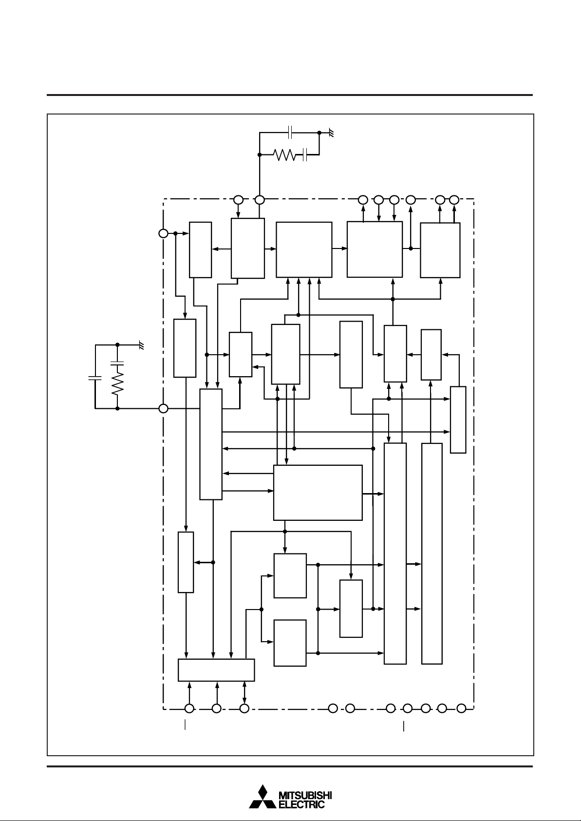
BLOCK DIAGRAM
3
SCREEN CHARACTER and PATTERN DISPLAY CONTROLLERS
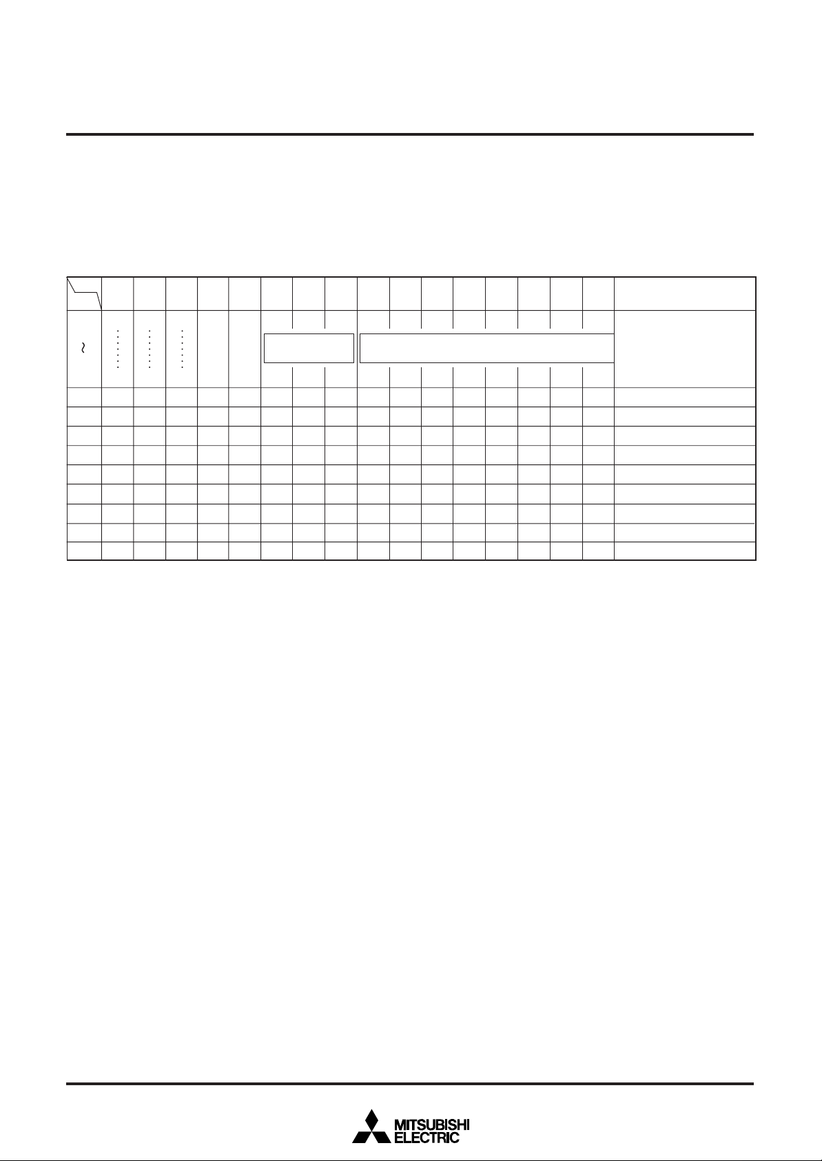
MEMORY CONSTITUTION
Address 0016 to EF16 are assigned to the display RAM, address F016
to F816 are assigned to the display control registers.
The internal circuit is reset and all display control registers (address
F016 to F816) are set to “0” and display RAM (address 0016 to EF16)
are RAM erased when the AC pin level is “L”.
__
MITSUBISHI MICROCOMPUTERS
M35053-XXXSP/FP
Set “0” in any of bits DAD through DAF of addresses 0016 through
EF16, and of bits DAE and DAF of addresses F016 through F816.
TESTn (n : a number) is MITSUBISHI test memory, so be sure to
observe the setting conditions.
Bit
DAF
DAE
DAD
DAC
DAB
DAA
Address
0016
EF16
F016
F116
F216
F316
F416
F516
F616
F716
F816
0
0
0
REV
BLINK
Reversed
Blinking
character
0
0
0
0
0
0
0
0
0
0
0
0
0
0
0
0
0
0
0
0
0
TEST25
TEST26
TEST27
TEST28
TEST29
TEST30
TEST31
TEST32
LEVEL1
REV
__________
W/R
DVP4
EVP4
___
D/V
TEST14
TEST19
TEST2
TEST24
EHP4
BLINK
TEST11
DVP3
EVP3
EFLD1
TEST13
______________
MB/LB
TEST1
RGBON
EHP3
DA9
EC2
EC1
Encode data or
character color
EC2
EC1
DECB1
TEST10
DVP1
DVP2
EVP1
EVP2
DFLD1
EFLD0
DSP9
SPACE
TEST16
TEST17
LBLACK
TEST0
TEST22
EHP2
__________
CL17/18
EHP1
Fig. 1 Memory constitution (M35053-XXXSP/FP)
DA8
EC0
EC0
DECB0
DVP0
EVP0
DFLD0
DSP8
TEST15
________
LIN24/32
CBLINK
EHP0
DA7
C7
C7
SYSEP1
SYSEP0
HP7
VP7
VSZ21
VSZ20
DSP7
DSP6
PALH
EQP
BLKHF
CURS7
CURS6
RAMERS
DSPON
DA6
C6
C6
HP6
VP6
BB
DA5
C5
C5
SEPV1
HP5
VP5
VSZ11
DSP5
MPAL
BG
CURS5
STOP1
DA4
C4
C4
SEPV0
HP4
VP4
VSZ10
HSZ21
DSP4
_______
INT/NON
BR
LEVEL0
CURS4
CURS3
STOPIN
SCOR
DA3
C3
C3
PTD1
HP3
VP3
DSP3
_______
N/P
DA2
C2
C2
PTD0
HP2
VP2
HSZ20
HSZ11
DSP2
BLINK2
BLINK1
PHASE2
PHASE1
CURS2
CURS1
EX
DA1
C1
C1
PTC1
HP1
VP1
DSP1
BLK1
DA0
Remarks
C0
Display RAMCharacter code
C0
Port output specify and so on
PTC0
Horizontal display start position and
HP0
Decode position specify
Vertical display start position and
VP0
Encode position specify
Character size and Encode EDecode
HSZ10
specify
Display mode specify
DSP0
Blinking specify and so on
BLINK0
Raster color specify
PHASE0
Cursor display specify
CURS0
Control display and so on
BLK0
4
SCREEN CHARACTER and PATTERN DISPLAY CONTROLLERS
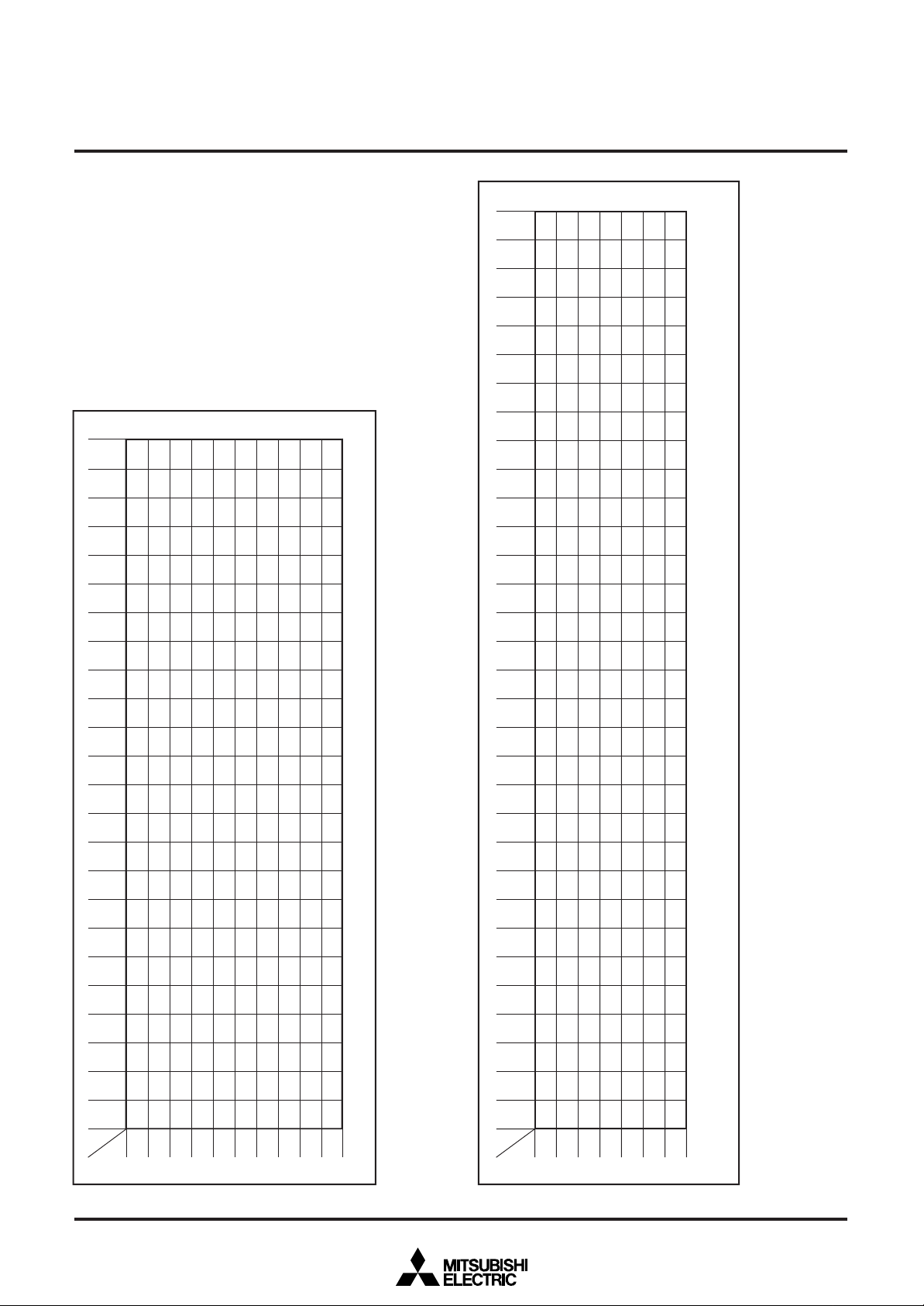
SCREEN CONSTITUTION
The screen lines and rows are determined from each address of the
display RAM. The screen consitution (24 characters ✕ 10 lines) is
shown in Figure 2 the screen constitution (32 characters ✕ 7 lines) is
shown in 3.
16
16
24
17
16
23
16
16
22
15
16
21
14
16
20
13
16
19
12
18
1116291641
17
101628164016581670
16
16
0F
16
15
0E
16
14
0D
16
13
0C
16
12
0B
16
11
0A
16
10
09
9
0816201638
16
8
07
16
7
06
16
6
05
16
5
04
16
4
03
16
3
02
2
01161916311649
16
1
00
1
Rows
Lines
16
16
5F
16
5E
16
5D
16
5C
16
5B
16
5A
16
77
16
76
16
75
16
74
16
73
16
72
16
8F
16
8E
16
8D
16
8C
8B16A3
8A16A2
16
2F
16
2E
16
2D
16
2C
16
2B
16
2A
16
47
16
46
16
45
16
44
16
43
16
42
16
5916711689
16
16
88
16
3F
16
3E
16
3D
16
3C
16
3B
16
3A
16
57
16
56
16
55
16
54
16
53
16
52
16
6F
16
6E
16
6D
16
6C
16
6B
16
6A
16
87
16
86
16
85
16
84
16
83
16
82
16
16
27
16
26
16
25
16
24
16
23
16
22
211639165116691681
16
50166816801698
16
16
4F
16
4E
16
4D
16
4C
16
4B
16
4A
16
16
67
16
66
16
65
16
64
16
63
16
62
16
7F
16
7E
16
7D
16
7C
16
7B
16
7A
1F
16
1E
16
1D
16
1C
16
1B
16
1A
16
37
16
36
16
35
16
34
16
33
16
32
6116791691
181630164816601678
16
2
3
4
5
6
16
A7
16
A6
16
A5
16
A4
16
16
16B916
A1
A016B8
16
9F
9E16B6
16
9D
16
9C
9B16B3
9A16B2
16
99
16
16
97
16
96
16
95
16
94
16
93
16
92
16
16
90
7
BF16D7
16
16
D6
BE
16
16
D5
BD
16
16
D4
BC
16
16
D3
BB
16
16
D2
BA
16
D1
16
16
D0
16
16
B7
CF
16
16
CE
16
16
B5
CD
16
16
B4
CC
16
16
CB
16
16
CA
16
16
B1
C9
16
16
B0
C8
16
AF16C7
16
16
C6
AE
16
16
C5
AD
16
16
C4
AC
16
16
C3
AB
16
16
C2
AA
16
16
A9
C1
16
A8
C016D8
8
9
16
EF
16
EE
16
ED
16
EC
16
EB
16
EA
16
E9
16
E8
16
E7
16
E6
16
E5
16
E4
16
E3
16
E2
16
E1
16
E0
16
DF
16
DE
16
DD
16
DC
16
DB
16
DA
16
D9
16
10
Note : The hexadecimal numbers in the boxes show the display RAM address.
Rows
32
31
30
29
28
27
26
25
24
23
22
21
20
19
18
17
16
15
14
13
12
11
10
9
8
7
6
5
4
3
2
1
Lines
MITSUBISHI MICROCOMPUTERS
M35053-XXXSP/FP
16
1F
3F165F167F169F
1E163E165E
16
1D
3D165D167D169D
1C163C165C
1B163B165B167B169B
1A163A165A
191639165916791699
16
181638
17163716571677
163616
16
15163516551675
16
14
34165416741694
1316331653
16
12
32165216721692
1116311651
101630165016701690
16
0F162F
0E162E164E166E
16
0D162D
0C162C164C166C
16
0B
2B164B166B168B
0A162A164A
16
09
29164916691689
0816281648
071627164716671687
0616261646
051625164516651685
16
041624
03162316431663
16
021622
01162116411661
16
00
20164016601680
1
2
16
16
16
7E169E
16
16
16
7C169C
16
167A169A16
16
16
5816781698
16
16
97
16
5616761696
16
16
95
16
16
16
731693
16
16
16
711691
16
16
4F166F168F
16
16
8E
16
4D166D168D
16
16
8C
16
166A16
16
8A
16
16
16
681688
16
16
16
661686
16
16
4416641684
16
16
83
16
4216621682
16
16
81
16
3
4
5
16
16
BF
DF
16
16
BE
DE
16
16
BD
DD
16
16
BC
DC
16
16
BB
DB
16
16
BA
DA
16
16
B9
D9
16
16
B8
D8
16
16
B7
D7
16
16
B6
D6
16
16
B5
D5
16
16
B4
16
B3
16
B2
16
B1
16
B0
16
AF
16
AE
16
AD
16
AC
16
AB
16
AA
16
A9
16
A8
16
A7
16
A6
16
A5
16
A4
16
A3
16
A2
16
A1
16
A0
6
16 to EF16.
D4
16
D3
16
D2
16
D1
16
D0
16
CF
16
CE
16
CD
16” to character code of addresses E0
16
CC
16
CB
16
CA
16
C9
16
C8
16
C7
16
C6
16
C5
16
C4
16
C3
16
C2
16
C1
16
C0
7
Notes 1. The hexadecimal numbers in the boxes show the display RAM address.
Notes 2. When 32 characters × 7 lines are displayed, set blank code “FF
Fig. 2 Screen constitution (24 characters ✕ 10 lines)
Fig. 3 Screen constitution (32 characters ✕ 7 lines)
5
MITSUBISHI MICROCOMPUTERS
M35053-XXXSP/FP
SCREEN CHARACTER and PATTERN DISPLAY CONTROLLERS
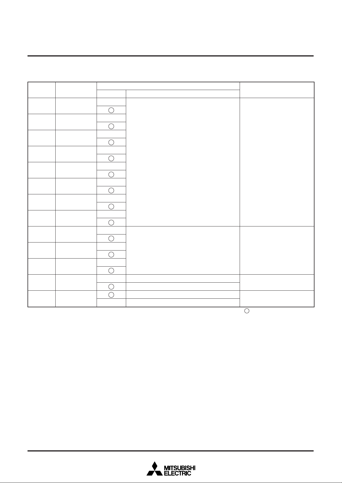
Display RAM DESCRIPTION
Display RAM Address 0016 to EF16
DA
0~C
0
1
2
3
4
5
6
7
8
9
A
B
C
Note. Resetting at the AC pin RAM-erases the display RAM, and the status turns as indicated by the mark around in the status column.
Name
C0
(LSB)
C1
C2
C3
C4
C5
C6
C7
(MSB)
EC0
EC1
EC2
BLINK
REV
__
Status
0
1
0
1
0
1
0
1
0
1
0
1
0
1
0
1
0
1
0
1
0
1
0
1
0
1
Set ROM-held character code of a character needed
to display.
When EFILD1, 0=1, 0 or 0, 1, set code of the data
needed to encode.
When RGBON=1, set background color by character
unit.
No blinking
Blinking
Normal character
Reversed character
Contents
Function
Remarks
Refer to encode function.
Refer to supplemental
explanation (4).
Refer to BLINK2 to 0
(address F516)
6
Display control register
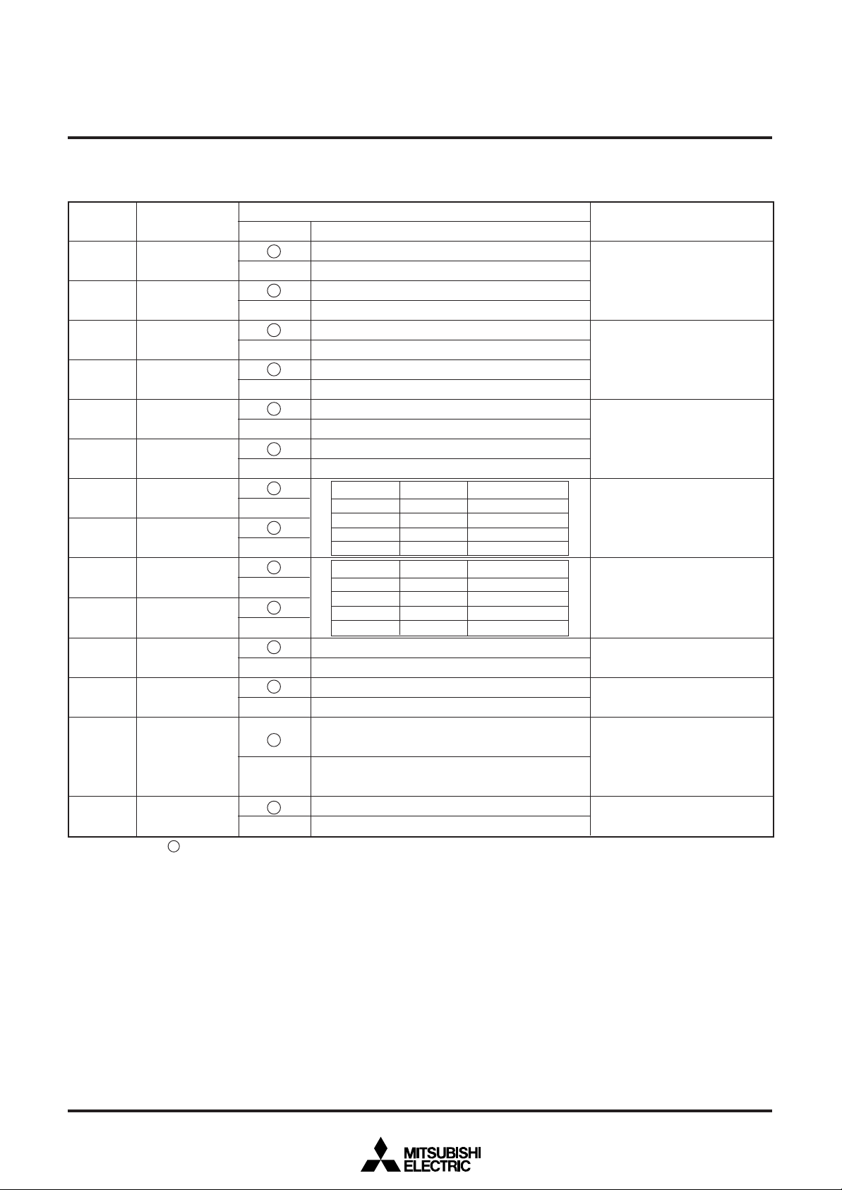
(1) Address F016
DA
0~D
0
1
2
3
4
5
6
7
8
9
A
B
C
Register
PTC0
PTC1
PTD0
PTD1
SEPV0
SEPV1
SYSEP0
SYSEP1
DECB0
DECB1
TEST10
TEST11
____
W/R
Status
0
1
0
1
0
1
0
1
0
1
0
1
0
1
0
1
0
1
0
1
0
1
0
1
0
1
MITSUBISHI MICROCOMPUTERS
M35053-XXXSP/FP
SCREEN CHARACTER and PATTERN DISPLAY CONTROLLERS
Contents
Function
P0 output (port 0)
BLNK1 output
P1 output (port 1)
CO1 output
It is negative polarity at P0 output “L”, BLINK1 output.
It is positive polarity at P0 output “H”, BLINK1 output.
It is negative polarity at P01 output “L”, CO1 output.
It is positive polarity at P01 output “H”, CO1 output.
It should be fixed to “0”.
Can not be used.
It should be fixed to “0”.
Can not be used.
SYSEP1
0
0
1
1
DECB1
0
0
1
1
Can not be used.
It should be fixed to “1”.
It should be fixed to “0”.
Can not be used.
Input data from SIN pin
Output data from SIN pin (Note 2)
SYSEP0
0
1
0
1
DECB0
0
1
0
1
Bias potential
Can not be used.
Can not be used.
1.75V
Can not be used.
Bias potential
2.35V
Can not be used.
Can not be used.
Can not be used.
Remarks
Port output control
Refer to supplemental explanation (5).
Control the port data
Refer to supplemental explanation (5).
Specifies the vertical synchronous
separation criterion
Refer to supplemental explanation (1).
Specifies the sync-bias potential
Specifies the decoding bias
potential
Control data I/O
Refer to decode data output
timing.
D
Notes 1.__The mark around the status value means the reset status by the “L” level is input to AC pin.
Notes 2.
Not necessary to release after setting W/R to “1”. Turn CS to “H” to switch over to input mode.
TEST25
0
1
It should be fixed to “0”.
Can not be used.
__
___
7
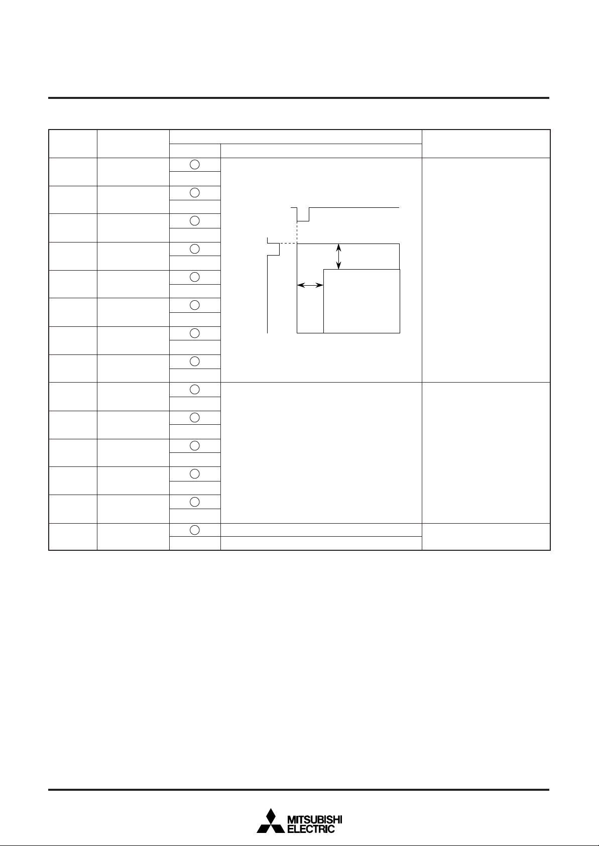
(2) Address F116
DA
0~D
0
1
2
3
4
5
6
7
8
9
A
B
C
D
Register
HP0
(LSB)
HP1
HP2
HP3
HP4
HP5
HP6
HP7
(MSB)
DVP0
(LSB)
DVP1
DVP2
DVP3
DVP4
(MSB)
TEST26
Status
0
1
0
1
0
1
0
1
0
1
0
1
0
1
0
1
0
1
0
1
0
1
0
1
0
1
0
1
SCREEN CHARACTER and PATTERN DISPLAY CONTROLLERS
Contents
Function
Let horizontal display start position be HS,
HS = T ✕ ( Σ 2nHPn+6)
n=0
7
HOR
VS
VERT
HS
Character
displaying
area
T : The oscillation cycle of display clock
Let the slice lines be DVS,
4
DVS = Σ 2nDVPn+6
n=0
It should be fixed to “0”.
Can not be used.
MITSUBISHI MICROCOMPUTERS
M35053-XXXSP/FP
Remarks
Set the horizontal display start
position by use of HP7 through
HP0. HP7 to HP0 = (00000000)
to (00001111) setting is
forbidden.
It can be set this up to 240 steps
in increments of one T.
Set the slice lines (horizontal
scanning lines) under decoding
by use of DVP4 through DVP0.
DVP4 to DVP0 = (00000) to
(00011) setting is forbidden.
Thus, it can be defined a setting
up to 26 steps covered by a
range from line 10 to line 35.
Refer to supplemental
explanation (2) about slice lines
(DVS).
8
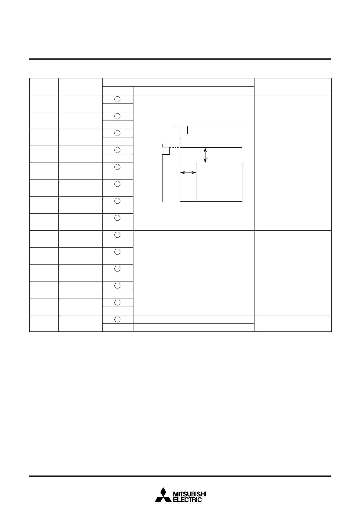
(3) Address F216
0~D
0
1
2
3
4
5
6
7
8
9
A
B
C
D
Register
VP0
(LSB)
VP1
VP2
VP3
VP4
VP5
VP6
VP7
(MSB)
EVP0
(LSB)
EVP1
EVP2
EVP3
EVP4
(MSB)
TEST27
Status
0
1
0
1
0
1
0
1
0
1
0
1
0
1
0
1
0
1
0
1
0
1
0
1
0
1
0
1
SCREEN CHARACTER and PATTERN DISPLAY CONTROLLERS
ContentsDA
Function
Let vertical display start position be VS,
VS = H ✕ Σ 2nVPn
n=0
7
HOR
VS
VERT
HS
Character
displaying
area
H : The oscillation cycle of horizontal
synchronous signal
Let the encode lines be EVS,
4
EVS = Σ 2nEVPn+6
n=0
It should be fixed to “0”.
Can not be used.
MITSUBISHI MICROCOMPUTERS
M35053-XXXSP/FP
Remarks
Set the vertical display start
position by use of VP7 through
VP0. VP7 to VP0 = (00000000)
to (00000110) setting is
forbidden.
It can be set this up to 249 steps
in increments of one H.
VP7 to VP0 = (00000000) to
(00100011) setting is forbidden
under encoding or decoding.
Sets the lines (horizontal
scanning lines) under encoding
by use of EVP4 through EVP0.
EVP4 to EVP0 = (00000) to
(00011) setting is forbidden.
Thus, it can be defined a setting
up to 26 steps covered by a
range from line 10 to line 35.
Refer to supplemental
explanation (2) about the encode
lines (EVS).
9
MITSUBISHI MICROCOMPUTERS
SCREEN CHARACTER and PATTERN DISPLAY CONTROLLERS
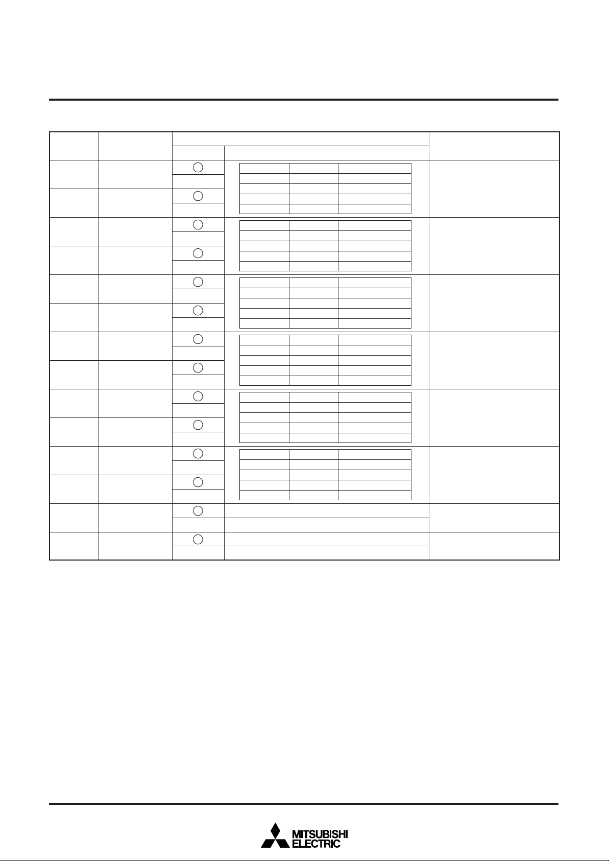
(4) Address F316
HSZ11
0
0
1
1
HSZ21
0
0
1
1
VSZ11
0
0
1
1
VSZ21
0
0
1
1
DFLD1
0
0
1
1
EFLD1
0
0
1
1
ContentsDA
Function
HSZ10
0
1
0
1
HSZ20
0
1
0
1
VSZ10
0
1
0
1
VSZ20
0
1
0
1
DFLD0
0
1
0
1
EFLD0
0
1
0
1
Horizontal direction size
1T/dot
2T/dot
3T/dot
4T/dot
Horizontal direction size
1T/dot
2T/dot
3T/dot
4T/dot
Vertical direction size
1H/dot
2H/dot
3H/dot
4H/dot
Vertical direction size
1H/dot
2H/dot
3H/dot
4H/dot
Field detection
OFF
The first field
The second field
Can not be used
Field detection
OFF
The first field
The second field
Can not be used
0~D
0
1
2
3
4
5
6
7
8
9
A
B
C
D
Note. Output buffer is needed with EDO (12-pin) at D/V= “1”. (Refer to example of peripheral circuit)
Register
HSZ10
HSZ11
HSZ20
HSZ21
VSZ10
VSZ11
VSZ20
VSZ21
DFLD0
DFLD1
EFILD0
EFLD1
___
D/V
TEST28
Status
0
1
0
1
0
1
0
1
0
1
0
1
0
1
0
1
0
1
0
1
0
1
0
1
0
1
0
1
It outputs digital signal.
It outputs composite video signal (Note).
It should be fixed to “0”.
Can not be used.
___
M35053-XXXSP/FP
Remarks
Character size setting in the
horizontal direction for the first
line.
Character size setting in the
horizontal direction for the 2nd
line to 10th line.
Character size setting in the
vertical direction for the first line.
Character size setting in the
vertical direction for the 2nd line
to 10th line.
Specifies the field determination
procedure in relation to the
Decoding functions.
Refer to supplemental
explanation (2).
Specifies the field determination
procedure in relation to the
Encoding functions.
Refer to supplemental
explanation (2).
Encode (EDO) output control.
Refer to encode function (3).
10
(5) Address F416
0~D
0
1
2
3
4
5
6
7
8
9
A
B
C
D
Register
DSP0
DSP1
DSP2
DSP3
DSP4
DSP5
DSP6
DSP7
DSP8
DSP9
SPACE
TEST13
TEST14
TEST29
Status
0
1
0
1
0
1
0
1
0
1
0
1
0
1
0
1
0
1
0
1
0
1
0
1
0
1
0
1
SCREEN CHARACTER and PATTERN DISPLAY CONTROLLERS
ContentsDA
Function
BLK1
BLK0
0
0
1
1
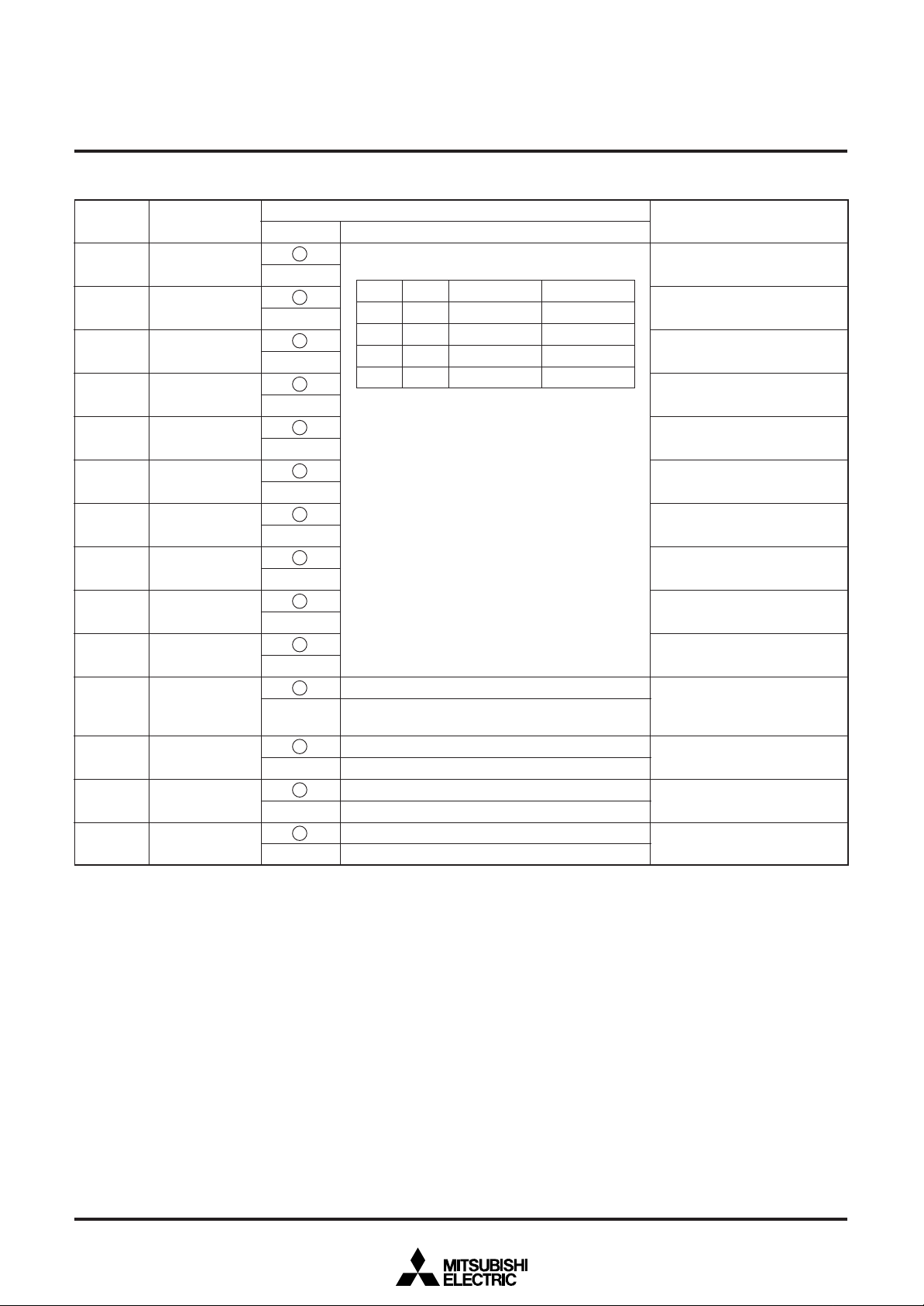
Depends on BLK0 and BLK1 (address F816)
DSPn in the generic name for DSP0 to DSP9.
DSP0 to DSP9 are each controlled independently.
Normal display
Put a space line between line 2 and line 3, and
between line 8 and line 9.
It should be fixed to “0”.
Can not be used.
It should be fixed to “0”.
Can not be used.
It should be fixed to “0”.
Can not be used.
DSPn= “1”
Matrix-outline border
0
size
1
Border size
Matrix-outline size
0
1
Character size
DSPn= “0”
Matrix-outline size
Character size
Border size
Matrix-outline size
MITSUBISHI MICROCOMPUTERS
M35053-XXXSP/FP
Remarks
Set the display mode of line 1.
Set the display mode of line 2.
Set the display mode of line 3.
Set the display mode of line 4.
Set the display mode of line 5.
Set the display mode of line 6.
Set the display mode of line 7.
Set the display mode of line 8.
Set the display mode of line 9.
Set the display mode of line 10.
Put a space line between line 2
and line 3 in displaying 32
characters.
11
SCREEN CHARACTER and PATTERN DISPLAY CONTROLLERS
(6) Address F516
BLINK0
0
0
1
1
_
N/P
0
0
1
1
PALH
0
1
ContentsDA
Function
BLINK1
0
1
0
1
MPAL
0
1
0
1
__
INT/NON
0
1
0
1
0~D
0
Register
BLINK0
Status
0
1
1
BLINK1
0
1
0
2
BLINK2
1
_
3
4
N/P
______
INT/NON
0
1
0
1
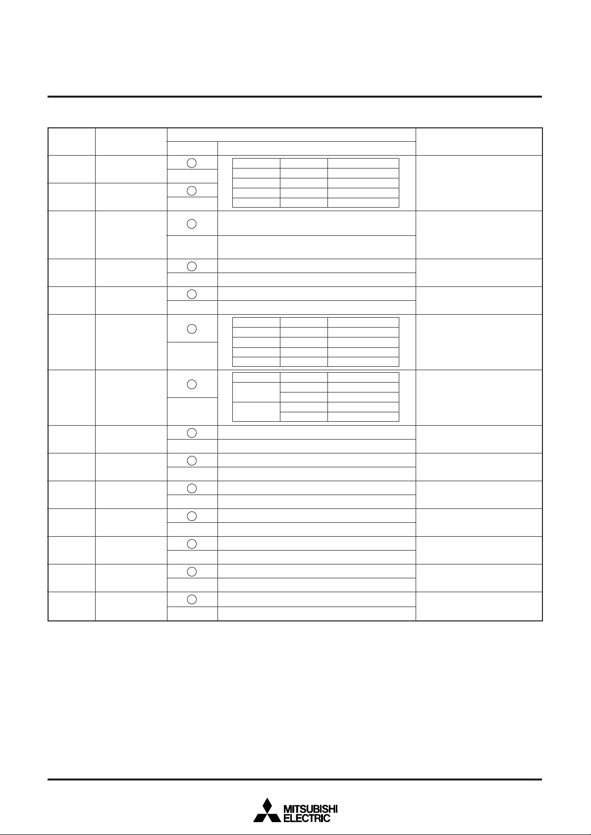
Division of vertical synchronizing signal into 1/64.
Cycle approximately 1 second.
Division of vertical synchronizing signal into 1/32.
Cycle approximately 0.5 second.
NTSC, M-PAL mode
PAL mode
Interlace
Non interlace
0
5
MPAL
1
0
6
PALH
1
7
EQP
0
1
8
TEST15
0
1
9
TEST16
0
1
A
TEST17
0
1
______________
B
MB/LB
0
1
C
TEST19
0
1
D
TEST30
0
1
Not include the equivalent pulse.
Include the equivalent pulse.
It should be fixed to “0”.
Can not be used.
It should be fixed to “0”.
Can not be used.
It should be fixed to “0”.
Can not be used.
Output from MSB side
Output from LSB side
It should be fixed to “0”.
Can not be used.
It should be fixed to “0”.
Can not be used.
Note. To blink a character, set 1 to DAB (the blinking bit) of the display RAM.
MITSUBISHI MICROCOMPUTERS
Duty
Blinking off
25%
50%
75%
Synchronous mode
NTSC
M-PAL
PAL
Not available
Number of scanning lines
625H lines
626H lines
627H lines
628H lines
M35053-XXXSP/FP
Remarks
Blinking duty ratio can be
altered. (Note)
Blinking cycle can be altered.
Refer to register MPAL
Scanning lines control (only in
internal synchronization)
Synchronizing signal is selected
with this register and N/P
register.
It should be fixed to “0” at NTSC
Effective only at non-interlace
Setting the decode data output
form
_
12
(7) Address F616
0~D
0
1
2
Register
PHASE0
PHASE1
PHASE2
Status
0
1
0
1
0
1
PHASE2
0
0
0
0
1
1
1
1
MITSUBISHI MICROCOMPUTERS
M35053-XXXSP/FP
SCREEN CHARACTER and PATTERN DISPLAY CONTROLLERS
ContentsDA
PHASE1
0
0
1
1
0
0
1
1
Function
PHASE0
Raster
0
1
0
1
0
1
0
1
Black
Red
Green
Yellow
Blue
Magenta
Cyan
White
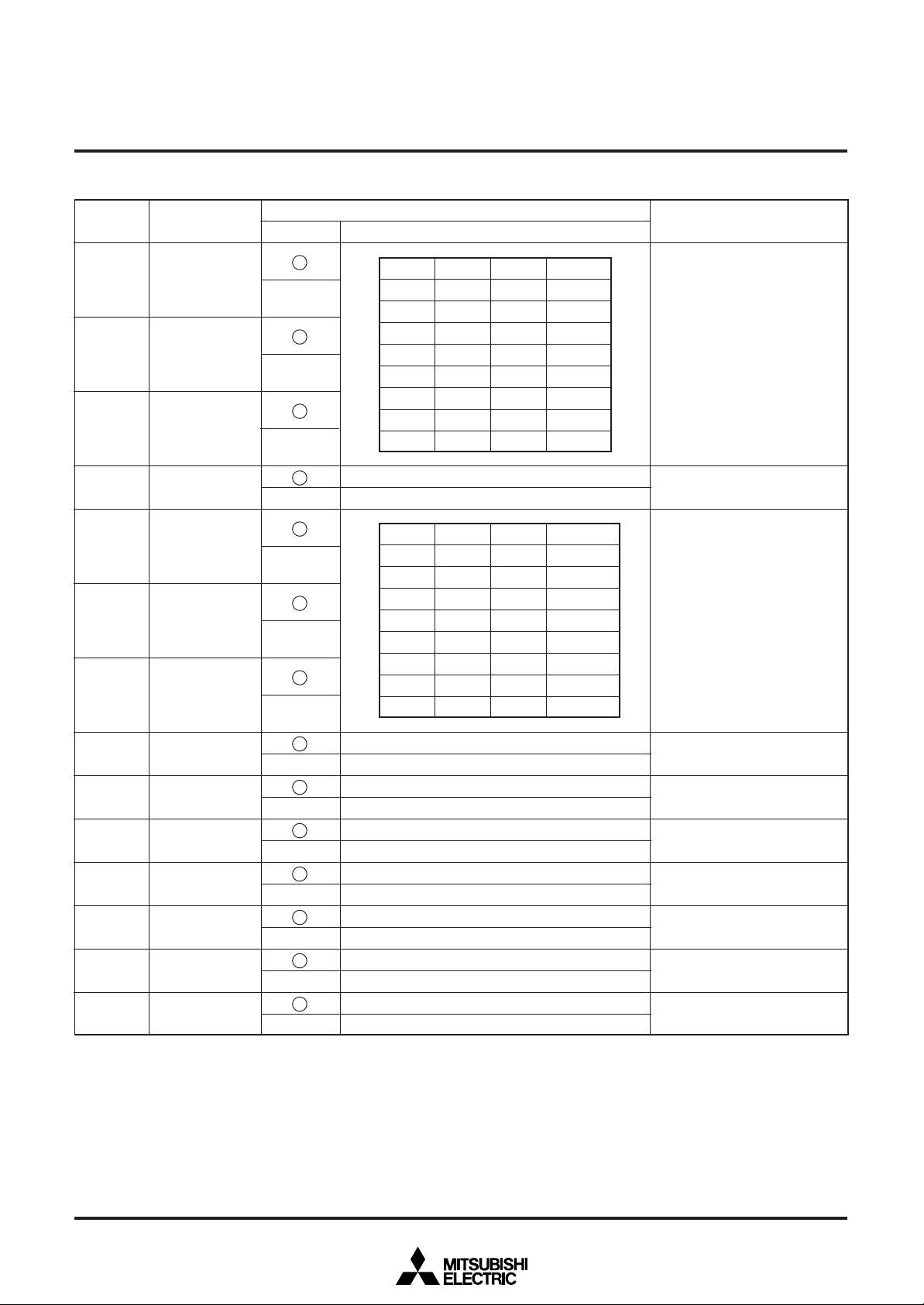
Raster color setting
Refer to supplemental
explanation (3) about video
signal level
Remarks
3
4
5
6
7
8
9
A
B
C
D
Note. It is neccessary to input the external composite video signal to the CVIN pin, and externally connect a 100 to 200Ω register in series.
LEVEL0
BR
BG
BB
BLKHF
__________
LIN24/32
LBLACK
TEST0
TEST1
TEST2
TEST31
0
1
0
1
0
1
0
1
0
1
0
1
0
1
0
1
0
1
0
1
0
1
Internal bias off
Internal bias on
BB
0
0
0
0
1
1
1
1
The halftone displaying “OFF” in superimpose
The halftone displaying “ON” in superimpose
24 characters 5 10 lines display
32 characters 5 7 lines display
Blanking level I 2.3V
Blanking level II 2.1V
It should be fixed to “0”.
Can not be used.
It should be fixed to “0”.
Can not be used.
It should be fixed to “0”.
Can not be used.
Can not be used.
It should to be fixed to “1”.
BG
0
0
1
1
0
0
1
1
BR
0
1
0
1
0
1
0
1
Character back-
ground color
Black
Red
Green
Yellow
Blue
Magenta
Cyan
White
Generates bias potential for
composite video signals
Character background color
setting.
Refer to supplemental
explanation (3) about video
signal level
This register is available in the
superimpose displaying only. (Note)
“1” setting is forbidden under
encoding.
Set a blackness level
13
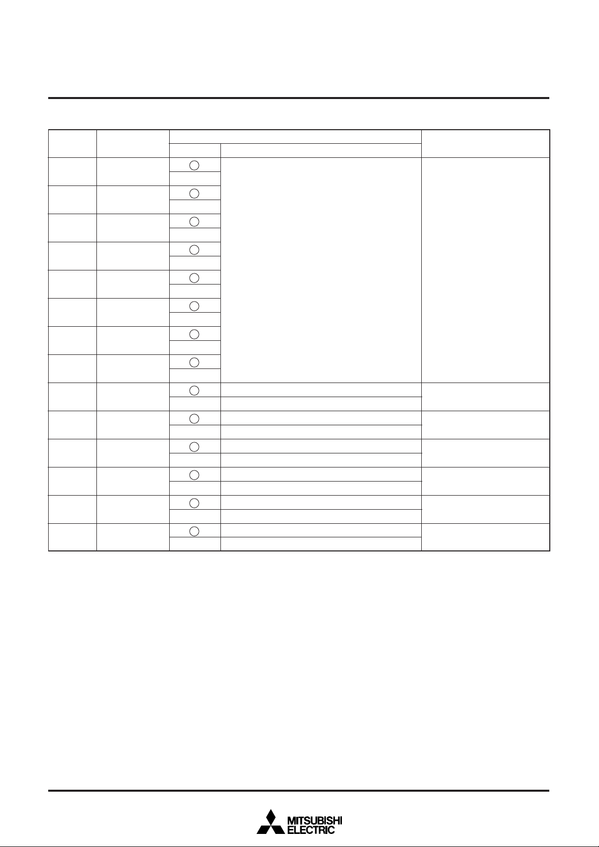
(8) Address F716
0~D
0
1
2
3
4
5
6
7
8
9
A
B
C
D
Register
CUR0
CUR1
CUR2
CUR3
CUR4
CUR5
CUR6
CUR7
CBLINK
__________
CL17/18
TEST22
RGBON
TEST24
TEST32
Status
0
1
0
1
0
1
0
1
0
1
0
1
0
1
0
1
0
1
0
1
0
1
0
1
0
1
0
1
MITSUBISHI MICROCOMPUTERS
SCREEN CHARACTER and PATTERN DISPLAY CONTROLLERS
ContentsDA
Function
Let cursor displaying address be CURS,
CURS = Σ 2nCURn
No blinking
Blinking
Cursor displaying at the 17th dot by vertical direction.
Cursor displaying at the 18th dot by vertical direction.
It should be fixed to “0”.
Can not be used.
Normal
Character background coloring
It should be fixed to “0”.
Can not be used.
It should be fixed to “0”.
Can not be used.
7
n=0
M35053-XXXSP/FP
Remarks
Set the cursor displaying
address by use of CUR7 through
CUR0.
CUR7 to CUR0 (11110000)
setting is forbidden under 24
characters display.
CUR7 to CUR0 (11100000)
setting is forbidden under 32
characters display.
Set CUR7 to CUR0 = (11111111)
under cursor is not be displayed.
The cursor displaying address
(CURS) is correspond to display
construction.
The cursor blinking setting
Refer to character construction.
Refer to supplemental
explanation (4).
14
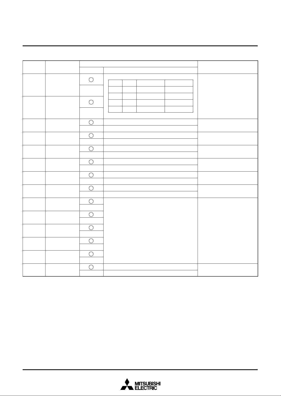
(9) Address F816
0~D
0
1
Register
BLK0
BLK1
Status
0
1
0
1
BLK1
0
0
1
1
MITSUBISHI MICROCOMPUTERS
M35053-XXXSP/FP
SCREEN CHARACTER and PATTERN DISPLAY CONTROLLERS
ContentsDA
BLK0
0
1
0
Matrix-outline size
1
Function
DSPn= “1”
Matrix-outline
border size
Border size
Character size
DSPn= “0”
Matrix-outline size
Character size
Border size
Matrix-outline size
Display mode
(BLNK output) variable
Remarks
2
3
4
5
6
7
8
9
A
B
C
D
Notes 1. In dealing with the internal synchronization, cut off external video signals outside the IC. The leakage of external input video signals
can be avoided.
Notes 2. In displaying color superimposition, enter into the OSCIN pin the fSC signal that phase-synchronizes with the color burst of the
composite video signals (input to the CVIN pin).
Notes 3. Erases all the display RAM. The character code turns to blank-FF16, the encode data bit and the blinking bit turn to “1” respectively,
and reversed character bit turns to “0”.
EX
SCOR
STOPIN
STOP1
DSPON
RAMERS
EHP0
EHP1
EHP2
EHP3
EHP4
LEVEL1
0
1
0
1
0
1
0
1
0
1
0
1
0
1
0
1
0
1
0
1
0
1
0
1
External synchronization
Internal synchronization
Superimpose monotone display
Superimpose coloring display (only NTSC)
fSC input mode
Can not be used.
Oscillation VCO for display
Stop oscillation VCO for display
Display OFF
Display ON
RAM not erased
RAM erased
Let encode data programming start position be EHS,
4
EHS = Σ 2nEHPn
n=0
Internal bias OFF
Internal bias ON
Synchronizing signal switching
(Note1)
“1” setting is forbidden at internal
synchronous or PAL, M-PAL
mode displaying.
OSCIN oscillation control
Control oscillation VCO for
display
This register does not exist
(Note 3).
Set encode start position by use
of EHP4 through EHP0.
EHP4 to EHP0 = (00000) to
(01111) is setting forbidden.
Refer to encode function (3)
Generates bias potential for decoding and synchronous separation.
15
 Loading...