

Page 1

Digital-Analog Converter
U
Digital-Analog Converter Module User's Manual
Module
Mitsubishi Programmable
Logic Controller
Q62DA
Q64DA
Q68DAV
Q68DAI
GX Configurator-DA
(SW0D5C-QDAU-E)
Page 2
A - 1 A - 1
• SAFETY PRECAUTIONS •
(Always read these instructions before using this equipment.)
Before using this product, please read this manual and the relevant manuals introduced in this manual
carefully and pay full attention to safety to handle the product correctly.
The instructions given in this manual are concerned with this product. For the safety instructions of the
PLC system, please read the user's manual of the CPU module to use.
In this manual, the safety instructions are ranked as "DANGER" and "CAUTION".
!
DANGER
CAUTION
!
Indicates that incorrect handling may cause hazardous conditions,
resulting in death or severe injury.
Indicates that incorrect handling may cause hazardous conditions,
resulting in medium or slight personal injury or physical damage.
Note that the !CAUTION level may lead to a serious consequence according to the circumstances.
Always follow the instructions of both levels because they are important to personal safety.
Please save this manual to make it accessible when required and always forward it to the end user.
[DESIGN PRECAUTION]
!
DANGER
•
Do not write data into the "system area" of the buffer memory of intelligent function modules.
Also, do not use any "prohibited to use" signals as an output signal to an inte lligent function
module from the PLC CPU.
Writing data into the "system area" or outputting a signal for "prohibited to use" may cause a
PLC system malfunction.
!
CAUTION
•
Do not bunch the control wires or communication cables with the main circuit or power wires, or
install them close to each other.
They should be installed 100mm(3.9inch) or more from each other.
Not doing so could result in noise that may cause malfunction.
Page 3

A - 2 A - 2
[INSTALLATION PRECAUTIONS]
!
CAUTION
•
Use the PLC in an environment that meets the general specifications contained in the user's
manual of the CPU module to use.
Using this PLC in an environment outside the range of the general specificat ions may cause
electric shock, fire, malfunction, and damage to or deterioration of the product.
•
When installing the module, securely insert the module fixing tabs into the mounting holes of the
base unit while pressing the installation lever located at the bott om of the module downward.
Improper installation may result in malfunction, breakdown or the module coming loose and
dropping.
Securely fix the module with screws if it is subject to vibration during use.
•
Tighten the screws within the range of specified torque.
If the screws are loose, it may cause the module to fallout, short circuits, or malfunction.
If the screws are tightened too much, it may cause damage to the screw and/or the module,
resulting in fallout, short circuits or malfunction.
•
Switch all phases of the external power supply off when mounting or removing the module.
Not doing so may cause damage to the module.
•
Do not directly touch the conductive area or electronic components of the module.
Doing so may cause malfunction or failure in the module.
[WIRING PRECAUTIONS]
!
CAUTION
•
Always ground the FG terminal for the PLC.
There is a risk of electric shock or malfunction.
•
When turning on the power and operating the module after wiring is completed, always attach
the terminal cover that comes with the product.
There is a risk of electric shock if the terminal cover is not attached.
•
Tighten the terminal screws within the range of specified torque.
If the terminal screws are loose, it may result in short circuits or malfunction.
If the terminal screws are tightened too much, it may cause damage to the screw and/or the
module, resulting in short circuits or malfunction.
•
Be careful not to let foreign matter such as sawdust or wire chips get inside the module.
They may cause fires, failure or malfunction.
•
The top surface of the module is covered with protective film to prevent foreign objects such as
cable offcuts from entering the module when wiring.
Do not remove this film until the wiring is complete.
Before operating the system, be sure to remove the film to provide adequate ventilation.
Page 4
A - 3 A - 3
[STARTING AND MAINTENANCE PRECAUTIONS]
!
CAUTION
•
Do not disassemble or modify the modules.
Doing so could cause failure, malfunction injury or fire.
•
Switch all phases of the external power supply off when mounting or removing the module.
Not doing so may cause failure or malfunction of the module.
•
Do not touch the connector while the power is on.
Doing so may cause malfunction.
•
Switch all phases of the external power supply off when cleaning or retightening the terminal
screws and module installation screws.
Not doing so may cause failure or malfunction of the module.
If the screws are loose, it may cause the module to fallout, short circuits, or malfunction.
If the screws are tightened too much, it may cause damages to the screws and/or the module,
resulting in the module falling out, short circuits or malfunction.
[DISPOSAL PRECAUTIONS]
!
CAUTION
•
When disposing of this product, treat it as industrial waste.
Page 5
A - 4 A - 4
REVISIONS
The manual number is given on the bottom left of the back cover.
Print Date Manual Number Revision
Dec., 1999 SH (NA)-080054-A
First printing
Oct., 2000 SH (NA)-080054-B Add the contents of the function version B.
Correction
About the Generic Terms and Abbreviations, Section 2.1, Section 3.1.3,
3.3.1, 3.4, Section 4.3, Section 5.2.1, 5.2.2, 5.3.3, 6.5.1
Partial addition
Section 1.1, Section 3.1.1, 3.1.2, 3.2.1, 3.2.2, 3.3.1, 3.3.2, 3.4.3, Section
4.5, Section 5.6.1, Section 7.2.3, 7.2.4
Addition
Section 1.2, Section2.2, Section 3.2.3, App-1, 1.1, 1.2, 1.3
Dec., 2000 SH (NA)-080054-C
Addition of Models
Q68DAV, Q68DAI
Correction
Section 3.2, 3.2.1, 3.2.2, 3.2.3, 3.3.1, 3.3.2, 3.4.1, 3.4.2, 3.4.3, 3.4.4,
3.4.6, 3.4.7, Section 4.5, Section 7.2.3, App-1.3
Partial addition
About the Generic Terms and Abbreviations, Product Structure,
Chapter 1, Section 1.1, Section 2.1, Section 3.1.1, 3.1.4, Section 4.1, 4.3,
Section 7.1, App-2
Jun., 2001 SH (NA)-080054-D Standardize the name from software package (GPP function) to Product
name (GX Developer).
Standardize the name from utility package (QDAU) to Product name (GX
Configurator-DA).
Correction
Conformation to the EMC Directive and Low Voltage Instruction, About
the Generic Terms and Abbreviations, Product Structure, Section 2.1,
2.2, Section 4.6, Section 5.2, 5.2.1, 5.2.2, 5.3.3, Appendix 1.2
Japanese Manual Version SH-080027-F
This manual confers no industrial property rights or any rights of any other kind, nor does it confer any patent
licenses. Mitsubishi Electric Corporation cannot be held responsible for any problems involving industrial property
rights which may occur as a result of using the contents noted in this manual.
1999 MITSUBISHI ELECTRIC CORPORATION
Page 6

A - 5 A - 5
INTRODUCTION
Thank you for purchasing the MELSEC-Q series PLC.
Before using the equipment, please read this manual carefully to develop full familiarity with the functions
and performance of the Q series PLC you have purchased, so as to ensure correct use.
Please forward a copy of this manual to the end user.
CONTENTS
SAFETY PRECAUTIONS..............................................................................................................................A- 1
REVISIONS....................................................................................................................................................A- 4
Conformation to the EMC Directive and Low Voltage Instruction ................................................................A- 8
About the Generic Terms and Abbreviations ................................................................................................A- 8
Product Structure ...........................................................................................................................................A- 9
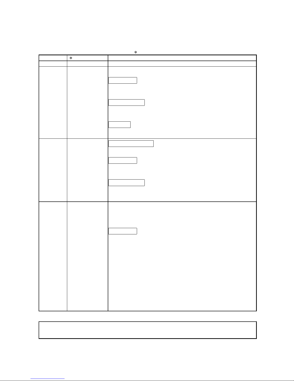
1 OVERVIEW 1- 1 to 1- 2
1.1 Features ..................................................................................................................................................1- 1
1.2 Functions Added by Function Version B................................................................................................1- 2
2 SYSTEM CONFIGURATION 2- 1 to 2- 4
2.1 Applicable Systems.................................................................................................................................2- 1
2.2 How to Check the Function Version and Software Version...................................................................2- 3
3 SPECIFICATIONS 3- 1 to 3-20
3.1 Performance Specifications....................................................................................................................3- 1
3.1.1 Performance specifications list ........................................................................................................3- 1
3.1.2 I/O conversion characteristics..........................................................................................................3- 2
3.1.3 Accuracy...........................................................................................................................................3- 9
3.1.4 Conversion speed ............................................................................................................................3- 9
3.2 D/A Conversion Module Function...........................................................................................................3-10
3.2.1 Synchronous output function ...........................................................................................................3-10
3.2.2 Analog output HOLD/CLEAR function............................................................................................. 3-11
3.2.3 Analog output test during PLC CPU STOP..................................................................................... 3-12
3.3 I/O Signals for the PLC CPU ..................................................................................................................3-13
3.3.1 List of I/O signals..............................................................................................................................3-13
3.3.2 Details of I/O signals ........................................................................................................................3-14
3.4 Buffer Memory......................................................................................................................................... 3-17
3.4.1 Buffer memory assignment..............................................................................................................3-17
3.4.2 D/A conversion enable/disable (buffer memory address 0: Un\G0)...............................................3-18
3.4.3 CH
digital values (buffer memory addresses 1 to 8: Un\G1 to Un\G8)......................................3-18
3.4.4 CH
set value check codes (buffer memory addresses 11 to 18: Un\G11 to Un\G18)...............3-19
3.4.5 Error codes (buffer memory address 19: Un\G19) .........................................................................3-19
3.4.6 Setting range (buffer memory address 20 and 21: Un\G20 and Un\G21) .....................................3-20
3.4.7 Offset/gain setting mode and offset/gain specification
(buffer memory addresses 22 and 23: Un\G22 and Un\G23)........................................................3-20
3.4.8 Setting value specification (buffer memory address 24: Un\G24)..................................................3-20
Page 7

A - 6 A - 6
4 SETUP AND PROCEDURES BEFORE OPERATION 4- 1 to 4-13
4.1 Handling Precautions..............................................................................................................................4- 1
4.2 Setup and Procedures before Operation ...............................................................................................4- 2
4.3 Part Identification Nomenclature ............................................................................................................4- 3
4.4 Wiring.......................................................................................................................................................4- 5
4.4.1 Wiring precautions............................................................................................................................4- 5
4.4.2 External wiring..................................................................................................................................4- 6
4.5 Switch Setting for Intelligent Function module.......................................................................................4- 8
4.6 Offset/Gain Settings................................................................................................................................ 4-11
5 UTILITY PACKAGE (GX Configurator-DA) 5- 1 to 5-18
5.1 Utility Package Functions........................................................................................................................5- 1
5.2 Installing and Uninstalling the Utility Package........................................................................................5- 2
5.2.1 User precautions ..............................................................................................................................5- 2
5.2.2 Operating environment.....................................................................................................................5- 4
5.3 Explanation of Utility Package Operation...............................................................................................5- 5
5.3.1 How to perform common utility package operations.......................................................................5- 5
5.3.2 Operation overview ..........................................................................................................................5- 8
5.3.3 Starting the intelligent function module utility .................................................................................. 5-10
5.4 Initial Setting............................................................................................................................................ 5-12
5.5 Automatic Refresh Settings....................................................................................................................5-13
5.6 Monitor/Test ............................................................................................................................................ 5-15
5.6.1 Monitor/test screen...........................................................................................................................5-15
5.6.2 Offset/gain setting operation............................................................................................................5-18
6 PROGRAMMING 6- 1 to 6- 5
6.1 Programming Example Using the Utility Package.................................................................................6- 2
6.1.1 Operating the utility package ...........................................................................................................6- 2
6.1.2 Programming example.....................................................................................................................6- 3
6.2 Programming Example without Using the Utility Package ....................................................................6- 4
7 TROUBLESHOOTING 7- 1 to 7- 5
7.1 Error Code List........................................................................................................................................7- 1
7.2 Troubleshooting ......................................................................................................................................7- 2
7.2.1 When the "RUN" LED is flashing or turned off................................................................................7- 2
7.2.2 When the "ERROR" LED is on or flashing......................................................................................7- 2
7.2.3 When an analog output value is not output.....................................................................................7- 3
7.2.4 Checking the D/A conversion module status using GX Developer system monitor......................7- 4
Page 8

A - 7 A - 7
APPENDIX App- 1 to App- 4
Appendix 1 Function upgrade for the D/A conversion module.................................................................App- 1
Appendix 1.1 A comparison of functions of the D/A conversion module..............................................App- 1
Appendix 1.2 Combinations of functions of the function version B D/A conversion module
and the GX Configurator-DA software version...............................................................App- 1
Appendix 1.3 Precautions when replacing the function version A module with function version B ....App- 2
Appendix 2. External Dimension Diagram ................................................................................................App- 3
INDEX Index- 1 to Index- 2
Page 9
A - 8 A - 8
Conformation to the EMC Directive and Low Voltage Instruction
For details on making Mitsubishi PLC conform to the EMC directive and low voltage
instruction when installin g it in your produc t, ple as e see Chapter 3, "EM C Direc ti ve
and Low Voltage Instruction" of the User's Manual (Hardware) of the CPU module to
use.
The CE logo is printed on the rating plate on the main body of the PLC that conforms
to the EMC directive and low voltage instruction.
By making this product conform to the EMC directive and low voltage instruction, it is
not necessary to make those steps individually.
About the Generic Terms and Abbreviations
Unless otherwise specified, this manual uses the following generic terms and
abbreviations.
Abbreviation/general terms Description of the abbreviation/general terms
D/A conversion module Generic term for Q62DA, Q64DA, Q68DAV Q68DAI
DOS/V personal computer IBM PC/AT® or compatible computer with DOS/V.
GX Developer
Generic product name of the product types SWnD5C-GPPW-E, SWnD5C-GPPW-EA,
SWnD5C-GPPW-EV and SWnD5C-GPPW-EVA.
"n" in the model name is 4 or greater.
GX Configurator-DA
Generic term for digital-analog conversion module setting and monitor tool GX
Configurator-DA (SW0D5C-QDAU-E)
QCPU (Q mode)
Generic term for Q00JCPU, Q00CPU, Q01CPU, Q02CPU, Q02HCPU, Q06HCPU,
Q12HCPU and Q25HCPU
Personal computer Generic term for DOS/V personal computer
Page 10
A - 9 A - 9
Product Structure
The product structure of this product is given in the table below.
Manual Name
Product name Quantity
Q62DA Q62DA Model Digital-Analog Conversion module 1
Q64DA Q64DA Model Digital-Analog Conversion module 1
Q68DAV Model Digital-Analog Conversion module 1
Q68DAV
FG terminal L-Shaped metal fitting 1
Q68DAI Model Digital-Analog Conversion module 1
Q68DAI
FG terminal L-Shaped metal fitting 1
SW0D5C-QDAU-E GX Configurator-DA Version 1(1-license product) (CD-ROM) 1
SW0D5C-QDAU-EA GX Configurator-DA Version 1(Multiple-license product) (CD-ROM) 1
Page 11

1 - 1 1 - 1
MELSEC-Q
1 OVERVIEW
1
1 OVERVIEW
This User's Manual describes the specifications, handling and programming methods
for the Q62DA type digital-analog conversion module (hereinafter referred to as the
Q62DA), the Q64DA type digital-analog conversion module (hereinafter referred to
as the Q64DA), the Q68DAV type digital-analog conversion module (hereinafter
referred to as the Q68DAV) and the Q68DAI type digital-analog conversion module
(hereinafter referred to as the Q68DAI) which are used in conjunction with MELSECQ series CPU module (hereinafter referred to as the PLC CPU).
In this manual, the Q62DA, Q64DA, Q68DAV and Q68DAI are collectively referred to
as the D/A (Digital-Analog) conversion modules.
1.1 Features
(1) Available models
• Q62DA
........
2 channels: Voltage or current output can be selected for each
channel.
• Q64DA
........
4 channels: Voltage or current output can be selected for each
channel.
• Q68DAV
........8 channels: All of which are voltage output.
• Q68DAI
........
8 channels: All of which are current output.
(2) High-speed conversion processing
Conversion processing is performed at a speed of 80 s/channel.
(3) High degree of accuracy
The conversion accuracy is ± 0.1% (When the ambient temperature is 25 ± 5 °C).
(4) Changing the resolution mode
The resolution mode can be changed according to the application, and digitalvalue resolution settings of 1/4000, 1/12000 or 1/16000 can be selected.
(5) Changing the output range
The output range
1
can easily be changed using GX Developer
.
1 The output range refers to the type of offset/gain settings. The most
frequently used range is set as the default but the user can also specify their
own offset/gai n set tin g s.
(6) Synchronous output function
This function sets a constant time (120 s) until the analog value is output after
the digital value is written from the PLC CPU. Highly accurate analog control can
be achieved by combining this function with a constant cycle execution type
program for the PLC CPU or the constant scan function
2.
2 The constant scan function executes the sequence program within a fixed
time interval.
(7) Analog output HOLD/CLEAR function
This function i s se t to ei th e r re tai n o r cl ea r th e an al og out pu t valu e wh en th e CP U
module is in the STOP status or when a stop error occurs.
Page 12
1 - 2 1 - 2
MELSEC-Q
1 OVERVIEW
1
(8) Easy settings using the utility package
A utility package is sold separately (GX Configurator-DA).
The utility package is not a required item. However, it can be used to set initial
settings and automatic refresh settings on screen, reduce sequence programs,
and check settings and operating status.
1.2 Functions Added by Function Version B
The functions added by the function version B D/A conversion module are listed below.
Item Function overview Reference section
Multiple PLC system
compatibility
Compatible with a Multiple PLC system. Section 2.1
Analog output test during
PLC CPU STOP
When the CH. output enable/disable flag is forced ON during PLC
CPU STOP, the D/A converted value is output.
Section 3.2.3
Resolution mode
The resolution mode can be changed according to the application, and
a resolution setting can be selected from 1/4000, 1/12000 and 1/16000.
Section 3.2
High resolution mode
status flag (X8)
This turns ON when in high resolution mode. Section 3.3
POINT
(1) See Appendix 1.1 for a comparison of functions of the function version.
(2) See Section 2.2 on how to check the function version.
Page 13
2 - 1 2 - 1
MELSEC-Q
2 SYSTEM CONFIGURATION
2
2 SYSTEM CONFIGURATION
2.1 Applicable Systems
This section describes the system configuration for the D/A conversion module.
(1) Applicable module and the number o f modules that can be installed
The following are the CPU module and network module (for remote I/O stations)
in which the D/A conversion module can be installed and the number of modules
that can be installed.
Applicable module
Number of modules that
can be installed
Remarks
Q02CPU
Q02HCPU
Q06HCPU
Q12HCPU
Q25HCPU
Maxi mum 64
Can be installed in Q mode only
(
1
)
Q00JCPU Max imum 16
CPU module
Q00CPU
Q01CPU
Maxi mum 24
(
1
)
Network module
QJ72LP25-25
QJ72BR15
QJ72LP25G
QJ71LP25GE
Maxi mum 64
MELSECNET/H Remote I/O
station (
2
)
1 See User's Manual (Function Explanation, Program Fundamentals) for the CPU module to use.
2 See Q Corresponding MELSECNET/H Network System Reference Manual (Remote I/O
network).
(2) Base unit in which the conversion module can be installed
The D/A conversion module can be installed in any I/O slot ( 3) of the base unit.
However, a power shortage may occur depending on the combination with other
installed modules and the number of modules used, so always take into
consideration the power supply capacity when installing modules.
3 Limited to the range of the number of I/O points in the CPU module and network module (for
remote I/O stations) .
(3) Compatibility with a multiple PLC system
First read the QCPU (Q mode) user's manual (Function Explanation, Program
Fundamentals) if the D/A conversion module is used with a multiple PLC system.
(a) Compatible D/A conversion module
Use a D/A conversion module with function version B or higher if using the
module in a multiple PLC system.
(b) Intelligent function module parameters
Perform PLC write of the intelligent function module parameters to the
control PLC of the D/A conversion module only.
Page 14

2 - 2 2 - 2
MELSEC-Q
2 SYSTEM CONFIGURATION
2
(4) Software packages supported
Correspondence between systems which use D/A conversion modules and
software packages are as shown below.
The GX Developer is necessary when using a D/A conversion module.
Software Version
GX Developer
GX Configurator-DA
4
If installed in the Q02/Q02H/Q06H/
Q12H/Q25HCPU
Version 4 or later
SW0D5C-QDAU-E 00A
or later
If installed in the
Q00J/Q00/Q01CPU
Version 7 or later
Version 1.10L or later
(cannot be used with the
SW0D5C-QDAU-E
60G or earlier versions).
If installed in a multiple PLC system Version 6 or later
SW0D5C-QDAU-E 20C
or later
If installed in a MELSECNET/H
remote I/O station
Version 6 or later
SW0D5C-QDAU-E 50F
or later
4 It is not compatible with the high resolution mode in SW0D5C-QDAU-E 10B or earlier versions.
See Appendix 1.2 for details.
Page 15
2 - 3 2 - 3
MELSEC-Q
2 SYSTEM CONFIGURATION
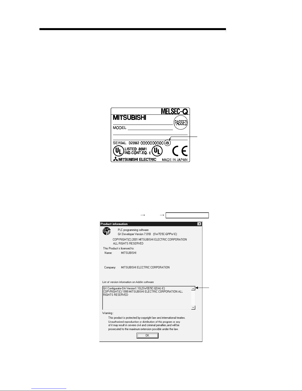
2.2 How to Check the Function Version and Softw are Ver si on
This section describes how to check the function version of the D/A conversion module
and the GX Configuration-DA software version.
(1) How to check the function version of the D/A conv ersi on modul e
(a) To check the version using the "SERIAL column of the rating plate" located
on the side of the module
Function version
(b) To check the version using the GX Developer
See Section 7.2.4 of this manual.
(2) How to check the GX Configuration-DA softwar e versi on
The GX Configuration-DA software version can be checked in GX Developer's
"Product information" screen.
[Startup procedure]
GX Developer "Help" Product information
Software version
(In the case of GX Developer Version 7)
Page 16

2 - 4 2 - 4
MELSEC-Q
2 SYSTEM CONFIGURATION
REMARK
The version indication for the GX Configurator-DA has been changed as shown
below from the SW0D5C-QDAU-E 60G upgrade product.
Previous product Upgrade and subsequent versions
SW0D5C-QDAU-E 60G
GX Configurator-DA Version 1.10L
Page 17
3 - 1 3 - 1
MELSEC-Q
3 SPECIFICATIONS
3
3 SPECIFICATIONS
3.1 Performance Specifications
3.1.1 Performance specifications list
Table 3.1 Performance specifications list
Model name
Item
Q62DA Q64DA Q68DAV Q68DAI
Number of analog output points 2 points (2 channels) 4 points (4 channels) 8 points (8 channels)
Digital input
16-bit signed binary (normal resolution mode: -4096 to 4095,
high resolution mode : -1 228 8 to 122 87 , - 1638 4 to 1638 3)
Voltage
–10 to 10 V DC (External load resistance value: 1 k
to 1M )
—
Analog
output
Current
0 to 20 mA DC
(External load resistanc e value: 0
to 600 )
—
0 to 20 mA DC
(External load resistance
value: 0
to 600 )
Normal resolution mode High resolu tion mode
Analog output range
Digital input value
Maximum
resolution
Digital input value
Maximum
resolution
0 to 5V 1.25 mV 0.416 mV
1 to 5V
0 to 4000
1.0 mV
0 to 12000
0.333 mV
-10 to 10V 2.5 mV -16000 to 16000 0.625 mV
Voltage
User range
setting
-4000 to 4000
0.75 mV -12000 to 12000 0.333 mV
0 to 20 mA 5 A1.66 A
4 to 20 mA
0 to 4000
4 A
0 to 12000
1.33
A
Current
User range
setting
-4000 to 4000 1.5
A -12000 to 12000 0.83 A
I/O characteristics,
Maximum resolution
Ambient temperature
25 ± 5 °C
Within ± 0.1 % (Voltage: ±10 mV, Current: ± 20
A)
Accuracy
(Accuracy in
respect to
maximum
analog
output value)
Ambient temperature
0 to 55 °C
Within ± 0.3 % (Voltage: ± 30 mV, Current: ± 60
A)
Conversion spe ed
80
s/channel
Voltage ± 12 V —
Absolute
maximum
output
Current 21 mA — 21 mA
Output short circuit protection Available
Insulation method
Between the I/O terminal and PLC power supply :
Between output cha nne ls :
Between ext e rnal supply power and ana log output :
Photo coupler ins u la t ion
No insula t io n
No insula t io n
Number of occupied points 16 points
Connected terminals 18-points terminal block
Applicable wire size 0.3 to 0.75 mm
2
Applicable solde rless terminal
R 1.25-3
(A solderles s te r minal w ith s le ev e ca nn ot b e used)
FG terminal: R1.25- 3, 1.2 5-YS3, R AV1. 25 - 3, V1.25- YS3 A
Other terminals th an F G: R1 .25- 3 ( A so ld erles s ter mina l
with sleeve cannot be used)
24 V DC + 20 %, – 15 %
Ripple, spike 50 0 mV P- P or l es s
Inrush current: 1.9 A,
within 300
s
Inrush current: 3.1 A,
within 300 s
Inrush current: 3.3 A,
within 70 s
Inrush current: 3.1 A,
within 75 s
External supp ly powe r
0.12 A0.18 A0.19 A0.28 A
Internal current consumption (5 V DC)
0.33 A0.34 A0.39 A0.38 A
Weight
0.19 kg 0.18 kg
REMARK
See the user's manual for the CPU module being used for the general specifications
for the D/A conversion module.
Page 18

3 - 2 3 - 2
MELSEC-Q
3 SPECIFICATIONS
3
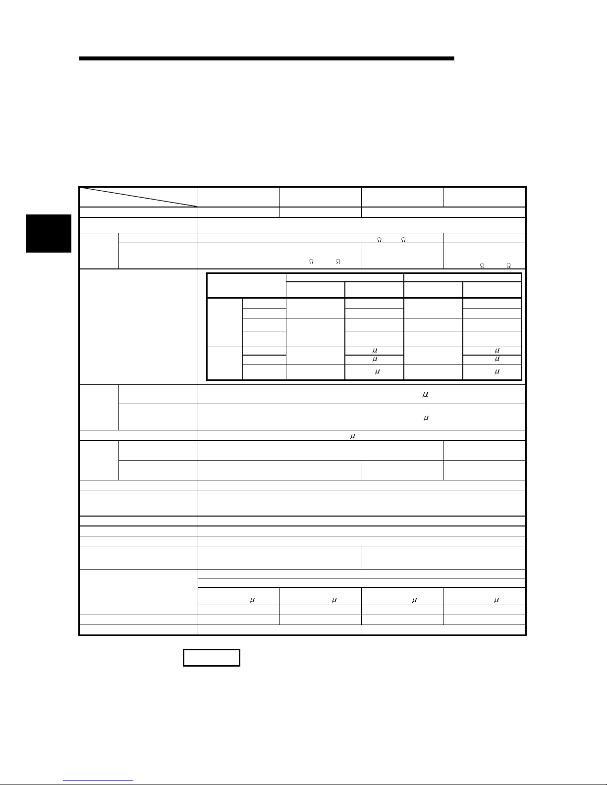
3.1.2 I/O conversion characteristics
I/O conversion cha ra cte ri st i cs are u sed fo r co nve rti ng th e di gi ta l value written fro m the
PLC CPU to an analog output value (voltage or current output), and represented by
inclined straight lines when offset and gain values are included.
Offset value
The offset value becomes the analog output value (voltage or current) when the digital
input value set from the PLC CPU is 0.
Gain value
The gain value denotes the analog output value (voltage or current) when the digital
input value set from the PLC CPU is
4000 (in normal resolution mode),
12000 (when 1 to 5V, 0 to 5V, 4 to 20 mA, 0 to 20 mA or the user range setting is
selected in high resol u tio n mode) ,
16000 (when -10 to 10V is selected in high resolution mode).
Page 19
3 - 3 3 - 3
MELSEC-Q
3 SPECIFICATIONS
(1) Voltage output characteristic
(a) Voltage output characteristic in normal resolution mode
Figure 3.1 shows a graph of the voltage output characteristic in normal
resolution mode.
Analog output value (V)
Digital input value
1)
2)
3)
4095
40002000-2000-4000-4096
-10
-5
0
5
10
Analog output pratical range
0
1
Number
Output value
range setting
Offset value Gain value Digital input value
Maximum
resolution
1) 1 to 5 V 1 V 5 V 1.0 mV
2) 0 to 5 V 0 V 5 V
0 to 4000
1.25 mV
3) –10 to 10 V 0 V 10 V –4000 to 4000 2.5 mV
—
User range setting
1 1
–4000 to 4000 0.75 mV
Figure 3.1 Voltage output characteristic in nor mal r esol ution mode
Page 20
3 - 4 3 - 4
MELSEC-Q
3 SPECIFICATIONS
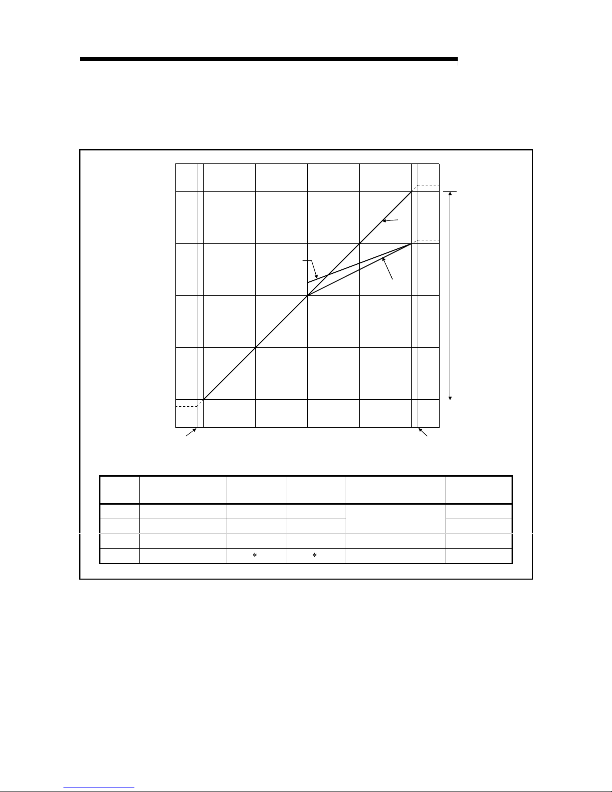
(b) Voltage output characteristic in high resolution mode
Figure 3.2 shows a graph of the voltage output characteristic in high
resolution mode.
Analog output value (V)
Digital input value
1)
2)
3)
16383160008000-8000-16000-16384
-10
-5
0
5
10
Analog output practical range
0
1
12000
12287
Number
Output value
range setting
Offset value Gain value Digital input value
Maximum
resolution
1) 1 to 5 V 1 V 5 V 0.333 mV
2) 0 to 5 V 0 V 5 V
0 to 12000
0.416 mV
3) –10 to 10 V 0 V 10 V –16000 to 16000 0.625 mV
—
User range setting
1 1
–12000 to 12000 0.333 mV
Figure 3.2 Voltage output characteristic in hig h r esoluti on mode
Page 21

3 - 5 3 - 5
MELSEC-Q
3 SPECIFICATIONS
POINT
(1) Set within the digi ta l in p ut rang e an d an al og ou tpu t rang e fo r each out pu t
range.
If these ranges are exceeded, the maximum resolution and accuracy may not
fall within the performance specifications. (Avoid using the dotted line area
shown in Figures 3.1 and 3.2.)
(2) Set the offset/gain values for the user setting range
1 within a range in which
the following conditions are satisfied.
(a) Setting range is from –10 to 10 V.
(b) { (Gain value) – (Offset value ) } > A
<Value of A>
Normal resolution mode High resolution mode
3.0 V 4.0 V
Page 22
3 - 6 3 - 6
MELSEC-Q
3 SPECIFICATIONS
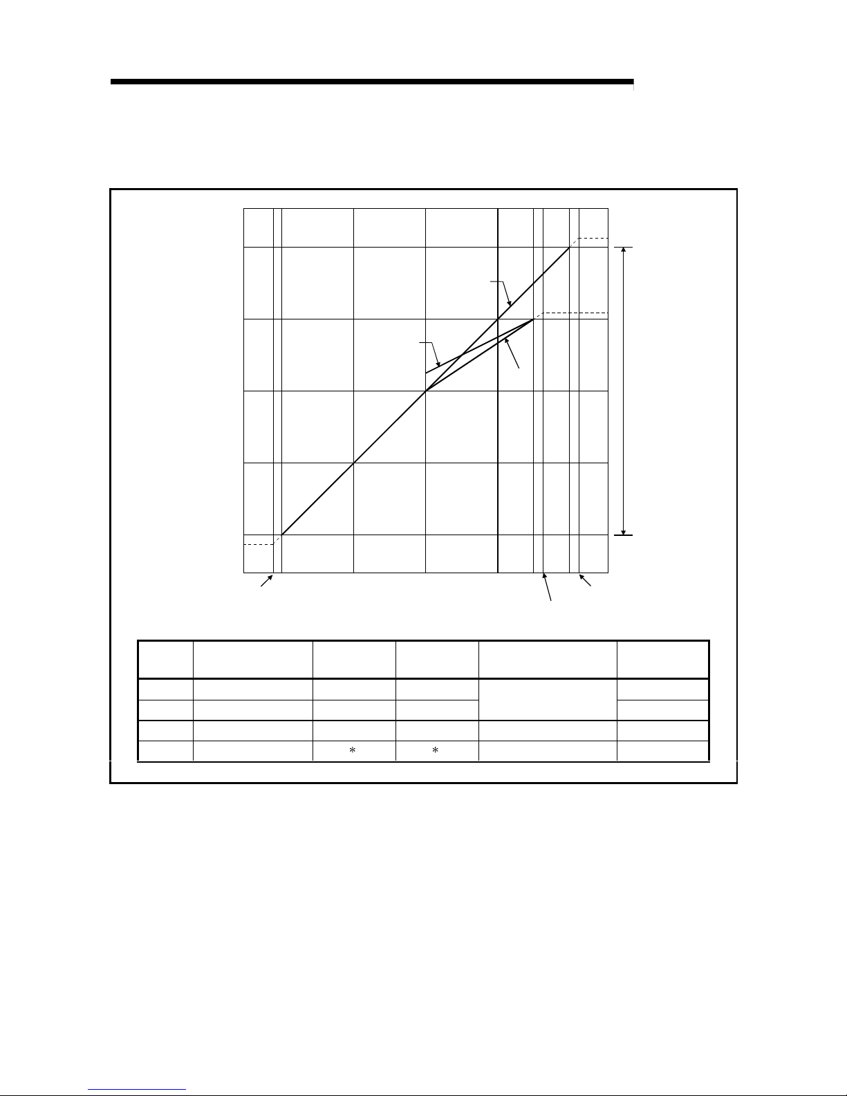
(2) Current output characteristic
(a) Current output characteristic in normal resolution mode
Figure 3.3 shows a graph of the current output characteristic in normal
resolution mode.
Analog output practical range
20
15
10
5
4
0
0 2000 4095
Digital input value
1)
2)
4000
Analog output value (mA)
Number
Output value
range setting
Offset value Gain value Digital input value
Maximum
resolution
1) 4 to 20 mA 4 mA 20 mA
4
A
2) 0 to 20 mA 0 mA 20 mA
0 to 4000
5
A
—
User range setting
1 1
–4000 to 4000
1.5
A
Figure 3.3 Current output characteristic in nor mal r esoluti on mode
Page 23
3 - 7 3 - 7
MELSEC-Q
3 SPECIFICATIONS
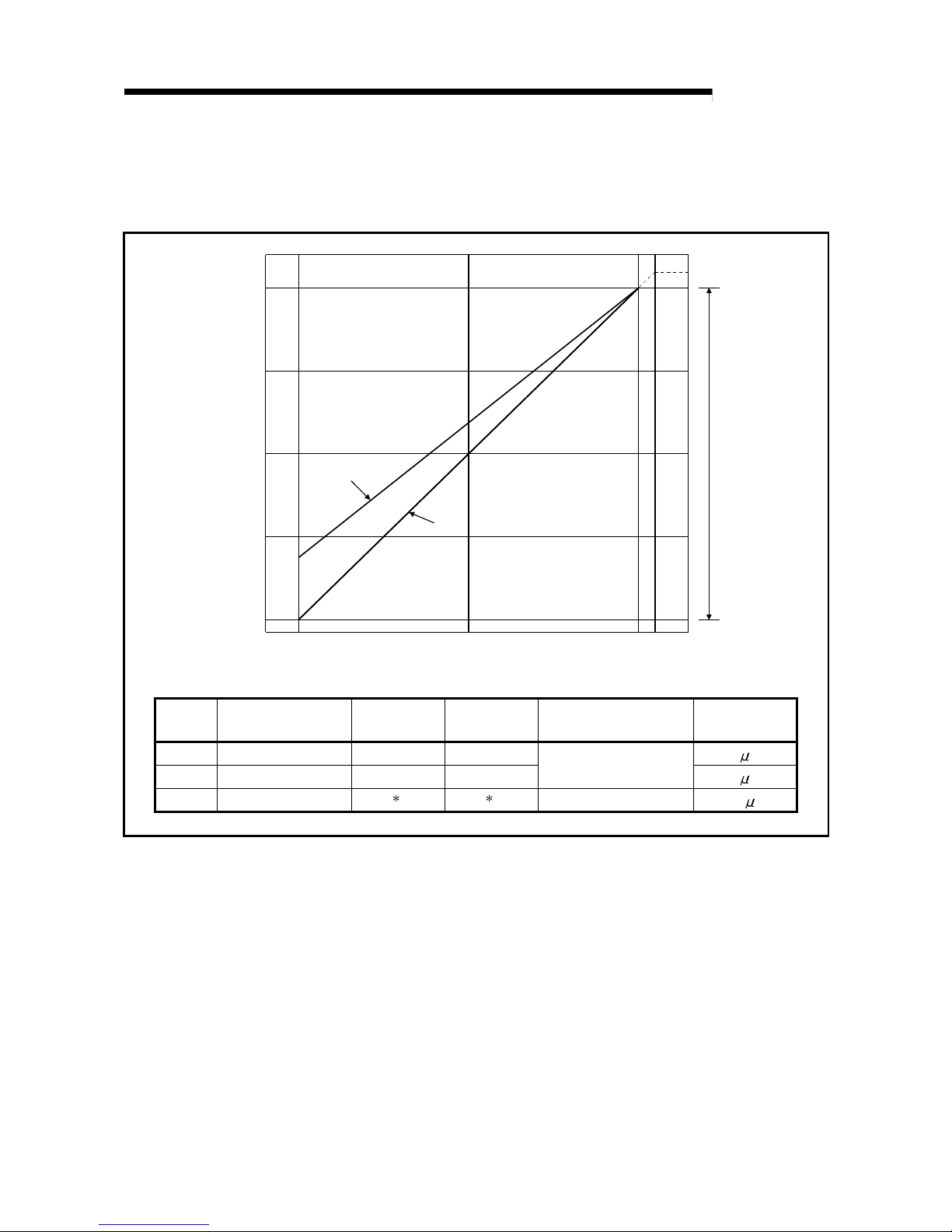
(b) Current output characteristic in high resolution mode
Figure 3.4 shows a graph of the current output characteristic in high
resolution mode.
20
15
10
5
4
0
0 6000 12287
Digital input vaule
1)
2)
12000
Analog output practical range
Analog output value (mA)
Number
Output value
range setting
Offset value Gain value Digital input value
Maximum
resolution
1) 4 to 20 mA 4 mA 20 mA
1.66
A
2) 0 to 20 mA 0 mA 20 mA
0 to 12000
1.33
A
—
User range setting
1 1
–12000 to 12000
0.83
A
Figure 3.4 Current output characteristic in hig h r esoluti on mode
Page 24
3 - 8 3 - 8
MELSEC-Q
3 SPECIFICATIONS
POINT
(1) Set within the digi ta l in p ut rang e an d an al og ou tpu t rang e fo r each out pu t
range.
If these ranges are exceeded, the maximum resolution and accuracy may not
fall within the performance specifications. (Avoid using the dotted line area
shown in Figures 3.3 and 3.4.)
(2) Set the offset/gain values for the user setting range
1 within a range in which
the following conditions are satisfied.
(a) Setting range is from 0 to 20 mA
(b) { (Gain value) – (Offset value ) } > A
<Value of A>
Normal resolution mode High resolution mode
6.0 mA 10.0 mA
Page 25

3 - 9 3 - 9
MELSEC-Q
3 SPECIFICATIONS
3.1.3 Accuracy
Accuracy is represented with respect to the maximum analog output value.
Accuracy does not change and remains within the range listed in the performance
specification even if the output characteristic is changed by changing offset/gain
settings, output range and resolution mode.
Figure 3.5 show s t he ra ng e o f fl u ctu at ion in accu r a cy wh en a -1 0 to 10V r ange is
selected and in normal resolution mode.
Accuracy for the analog output is within ± 0.1% (± 10 mV) when the ambient
temperature is 25 ± 5 °C and within ± 0.3% (± 30 mV) when the ambient temperature
is 0 to 55°C.
–10
–4000 0 +4000
Digital input value
Fluctuation range
10
Analog output value (V)
0
Figure 3.5 Accuracy
3.1.4 Conversion speed
The conversion speed per channel for the Q62DA, Q64DA, Q68DAV and Q68DAI is
"80
s the number of conversion enabled channels".
By setting the unused channels to D/A conversion disabled in buffer memory address
0 (Un\G0), the conversion speed can be increased.
Page 26
3 - 10 3 - 10
MELSEC-Q
3 SPECIFICATIONS
3.2 D/A Conversion Module Function
Table 3.2 shows the function of the D/A conversion modules.
Table 3.2 Function list
Item Function Reference section
D/A conversion
enable/disable function
(1) Specifies whether to enable or disable the D/A conversion for each channel.
(2) By disabling the D/A conversion for the channels that are not used, the
conversion speed can be shortened.
Section 3.4.2
D/A output
enable/disable function
(1) Specifies whether to output the D/A converted value or the offset value for
each channel.
(2) The conversion speed stays constant regardless of w hether D/A output is
enabled or disabled.
Section 3.3.1
Synchronous output
function
(1) An analog output synchronized with the PLC CPU can be obtained. Section 3.2.1
Analog output
HOLD/CLEAR function
(1) The output analog value can be retained when the PLC CPU module is
placed in the STOP status or when an error occurs.
Section 3.2.2
Analog output test
during PLC CPU STOP
(1) When the CH. output enable/disable flag is forced ON during PLC CPU
STOP, the D/A converted analog value is output.
Section 3.2.3
Resolution mode
(1) The resolution mode can be changed according to the application, and a
resolution setting can be selected from 1/4000, 1/12000 and 1/16 000.
(2) The resolution mode setting is applicable to all channel s.
(3) See Section 3.1.1 for the digital input values and maximum resolution in
normal resolution mode and high resolution mode.
Section 3.1.1
Section 4.5
3.2.1 Synchronous output function
An analog output that is synchronized with the PLC CPU can be obtained.
The analog output will be updated a fter the syn chronou s output requ est (YD) i s set to ON
and the time specified a s "PLC CPU p rocessi ng time + 120
s" has elapsed.
However, the ana log outp ut will b e fi xed t o CH1, an d oth e r ch ann el s ( CH2 t o CH8)
cannot be used.
Digital write from the
PLC CPU
Synchronous output
request (YD)
Analog output value
Always constant
<Program example>
Write command
DELTA YD
T0 K1 D0 K1H0
Digital value wri te
Outputs synchronous
output request as a pulse
Page 27

3 - 11 3 - 11
MELSEC-Q
3 SPECIFICATIONS
3.2.2 Analog output HOLD/CLEAR function
Whether the output analog value will be retained or cleared according to the PLC CPU
operating status (RUN, STOP, and Stop error) can be set using the intelligent function
module switch (see Section 4.5).
Table 3.3 lists available analog output status based on the combinations of D/A
conversion enable/disable and CH
output enable/disable.
Perform settings according to the system application.
Table 3.3 Analog output status combination lis t
D/A conversion
enable/disable
Setting (Un\G0)
Enable Disable
CH output
enable/disable
flags (Y1 to Y8)
Enable Disable Enable or disable
Setting
combination
execution
status
HOLD/CLEAR
setting
HOLD CLEAR HOLD or CLEAR HOLD or CLEAR
Analog output status when PLC
CPU is running
Outputs the analog value of
the D/A converted digital
value.
Offset 0 V/0 mA
Analog output status when PLC
CPU is stopped
Hold Offset Offset 0 V/0 mA
Analog output status when a
PLC CPU stop error occurs
Hold Offset Offset 0 V/0 mA
Analog output status when a
watchdog timer1 error occurs
in Q64DA, Q62DA, Q68DAV or
Q68DAI
0 V/0 mA 0 V/0 mA 0 V/0 mA 0 V/0 mA
1 This occurs when program operations are not completed within the scheduled time due to a hardware
problem of the D/A conversion module. When a watchdog timer error occurs, module READY (X0) turns
OFF and the D/A conversion module RUN LED turns off.
POINT
Design the system so that the D/A conversion enable/disable setting (Un\G0)
changes to "Enable" after the external power (see Section 4.3) is supplied.
Analog output may not properly be performed if the external power is not at the
specified voltage.
Page 28

3 - 12 3 - 12
MELSEC-Q
3 SPECIFICATIONS
3.2.3 Analog output test during PLC CPU STOP
When the PLC CPU stops, an analog output test as shown in Table 3.4 can be
performed.
The analog output test performs the following operations in GX Developer device
testing or GX Configurator-DA selection testing described in Section 5.6.1.
• Sets the output enable/disable flag (Y1 to Y8) for the channel to be tested to enable
(OFF
ON).
• Writes a digital value eq ui vale n t to th e an al og value t o be ou tp ut in C H.
digital
value (see Table 3.6 in Section 3.4.1) in the buffer memory.
This function is performed with the D/A conversion module of function version B or
later.
Table 3.4 List of analog output test
D/A conversion
enable/disable
Setting (Un\G0)
Enable Disable
Setting
combination
CH
output
enable/disable
flags (Y1 to Y8)
Enable Disable Enable disable
Analog output test Allowed
Not allowed
1
1 Perform the analog output test after changing the D/A conversion enable/ disabl e setting
(buffer memory address 0: Un\G0) to enable.
Page 29

3 - 13 3 - 13
MELSEC-Q
3 SPECIFICATIONS
3.3 I/O Signals for the PLC CPU
3.3.1 List of I/O signals
Table 3.5 shows a list of the I/O signals for the D/A conversion modules.
The following explanation is mentioned based on the Q68DAV and Q68DAI with 8channel analog output (CH.1 to CH.8).
Note that I/O numbers (X/Y) shown in this chapter and thereafter are the values when
the start I/O number for the D/A conversion module is set to 0.
Table 3.5 List of I/O signal
Signal direction D/A conversion module CPU module Signal direction CPU module D/A conversion module
Device No Signal name Device No. Signal name
X0 Module READY Y0
Use prohibited
1
X1 Y1 CH1 Output enable/disable flag
X2 Y2 CH2 Output enable/disable flag
X3
Y3
2
CH3 Output enable/disable flag
X4
Y4
2
CH4 Output enable/disable flag
X5
Y5
2
CH5 Output enable/disable flag
X6
Y6
2
CH6 Output enable/disable flag
X7
Use prohibited
1
Y7
2
CH7 Output enable/disable flag
X8 High resolution mode status flag
Y8
2
CH8 Output enable/disable flag
X9
Operating condition setting
completed flag
Y9 Operating condition setting request
XA Offset/gain setting mode flag YA User range writing request
XB Channel change completed flag YB Channel change request
XC Set value change completed flag YC Set value change request
XD Synchronous output mode flag YD Synchronous output request
XE
Use prohibited
1
YE
Use prohibited
1
XF Error flag YF Error clear request
POINT
1 These signals cannot be used by the user since they are used by the system. If
these are turned ON/OFF by the sequence program, the functioning of the D/A
conversion module cannot be guaranteed.
2 For Q62DA, Y3 to Y8 cannot be used.
For Q64DA, Y5 to Y8 cannot be used.
Page 30

3 - 14 3 - 14
MELSEC-Q
3 SPECIFICATIONS
3.3.2 Details of I/O signals
I/O signals for the D/A conversion module are explained in detail below.
(1) Input signals
Device No. Signal name Description
X0 Module READY
(1) When the PLC CPU is powered on or reset, this signal turns on once the
preparation for D/A conversion has been completed, and D/A conv ersion
processing is then performed.
(2) When the Module READY (X0) signal is off, D/A conversion processing is not
performed. Module READY (X0) turns off in the following situations:
• During offset/gain setting mode
• When the D/A conversion module has a watchdog timer error
X8
High resolution
mode status flag
(1) This turns ON when in high resolution mode.
X9
Operating
condition setting
completed flag
(1) This is used as an interlock condition for turning the operating condition setting
request (Y9) ON/OFF when the setting for D/A conversion enable/disable (buffer
memory address 0: Un\G0) is changed.
(2) Under the following conditions, the operating condition setting completed flag (X9)
turns OFF.
• When Module READY (X0) is OFF
• When operating condition setting request (Y9) is ON
Performed by the D/A conversion module
Performed by the sequence program
Module READY (X0)
Operating condition
setting completed flag (X9)
Operating condition
setting request (Y9)
XA
Offset/gain setting
mode flag
(1) This is used as an interlock condition for setting the user range write request (YA) to
ON/OFF when registering the value after adjustment of the offset/gain settin gs hav e
been completed.
(2) See Section 4.6 regarding the offset/gain settings.
Performed by the D/A conversion module
Performed by the sequence program
OFF
Module READY (X0)
Offset/gain setting mode flag (XA)
User range write request (YA)
Page 31

3 - 15 3 - 15
MELSEC-Q
3 SPECIFICATIONS
Device No. Signal name Description
XB
Channel change
completed flag
(1) This is used as an interlock condition for setting the channel cha nge reque st (YB) to
ON/OFF when changing the channel for which the offset/gain sett ings are to b e
performed.
(2) See Section 4.6 regarding the offset/gain settings.
Performed by the D/A conversion module
Performed by the sequence program
Channel change request (YB)
Offset/gain setting mode
Offset/gain specifications
(buffer memory addresse s 22 and 23:
Un\G22 and Un\G23)
Channel change completed
flag (XB)
XC
Set value change
completed flag
(1) This is used as an interlock condition for setting the set value c hange reque st (YC)
to ON/OFF when adjusting the offset/gain settings.
(2) See Section 4.6 regarding the offset and gain settings.
Performed by the D/A conversion module
Performed by the sequence program
Set value change request (YC)
Set value change completed
flag (XC)
XD
Synchronous
output mode flag
This flag turns ON when the system is set to the synchronous o utput mo de.
XF Error flag
(1) The error flag turns ON when a write error occurs.
(2) To turn the error flag (XF) OFF, remove the cause of the error and set the error
clear request (YF) to ON.
The error code (buffer memory address 19: Un\G19) changes to 0 and the ER RO R
LED turns off.
Performed by the D/A conversion module
Performed by the sequence program
Error flag (XF)
Error clear request (YF)
Error code is read during this interval.
Page 32

3 - 16 3 - 16
MELSEC-Q
3 SPECIFICATIONS
(2) Output signals
Device No. Signal name Description
Y1 to Y8
CH
output
enable/disable flag
(1) Specifies whether to output the D/A converted value or offset value for each
channel.
ON: D/A converted value OFF: Offset value
(2) The D/A conversion speed is constant regardless of whether the output
enable/disable flag is ON or OFF.
Y9
Operating
condition setting
request
(1) This turns ON when the contents of the D/A conversion enable/disable settin g are
validated.
(2) See the X9 column for the ON/OFF timing.
YA
User range write
request
(1) This turns ON when the values for the adjusted offset/gain settings are regi stered in
the D/A conversion module.
(2) See the XA column for ON/OFF timing.
See Section 4.6 for offset/gain settings.
YB
Channel change
request
(1) This turns ON when changing the channel for which offset/gain sett ings are to be
performed.
(2) See the XB column for the ON/OFF timing.
YC
Set value change
request
(1) This turns ON/OFF when increasing or decreasing the analog output value during
adjustment of the offset/gain settings.
(2) The analog output is either increased or decreased based on the value that was set
in buffer memory address 24 (Un\G24).
YD
Synchronous
output request
(1) While in the synchronous output mode, D/A conversion is performed and the analo g
value is output at the timing when the synchronous output reque st (Y D ) is set to
ON.
YF Error clear request
(1) This turns ON when a write error is cleared.
(2) See the XF column for ON/OFF timing.
Page 33

3 - 17 3 - 17
MELSEC-Q
3 SPECIFICATIONS
3.4 Buffer Memory
3.4.1 Buffer memory assignment
The following explanation is mentioned based on Q68DAV and Q68DAI with 8-channel
analog output (CH1 to CH8).
Table 3.6 Buffer memory assignment
Address
Hexadecimal Decimal
Description
Default
2
Read/write
3
0
H
0 D/A conversion enable/disable
Q62DA : 3
H
Q64DA : F
H
Q68DAV :
FF
H
Q68DAI :
FF
H
R/W
1
H
1 CH1 Digital value 0 R/W
2
H
2 CH2 Digital value 0 R/W
3
H
3
CH3 Digital value
1
0R/W
4
H
4
CH4 Digital value
1
0R/W
5
H
5
CH5 Digital value
1
0R/W
6
H
6
CH6 Digital value
1
0R/W
7
H
7
CH7 Digital value
1
0R/W
8
H
8
CH8 Digital value
1
0R/W
9
H
9 ——
A
H
10
System area
——
B
H
11 CH1 Set value check code 0 R
C
H
12 CH2 Set value check code 0 R
D
H
13
CH3 Set value check code
1
0R
E
H
14
CH4 Set value check code
1
0R
F
H
15
CH5 Set value check code
1
0R
10
H
16
CH6 Set value check code
1
0R
11
H
17
CH7 Set value check code
1
0R
12
H
18
CH8 Set value check code
1
0R
13
H
19 Error code 0 R/W
14
H
20 Setting range (CH1 to CH4)
Q62DA, Q64DA,
Q68DAI: 0
H
Q68DAV: 2222
H
R
15
H
21 Setting range (CH5 to CH8)
Q62DA, Q64DA,
Q68DAI: 0
H
Q68DAV: 2222
H
R
16
H
22
Offset/gain setting mode
Offset specification
0R/W
17
H
23
Offset/gain setting mode
Gain specification
0R/W
18
H
24 Offset/gain adjustment value specification 0 R/W
1 For Q62DA, buffer memory address for CH3 to CH8 is the system area.
For Q64DA, buffer memory address for CH5 to CH8 is the system area.
2 This is the initial value set after the power is turned on or the PLC CPU is reset.
3 Indicates whether reading and writing to/from a sequence program are enabled.
R : Reading enabled W : Writing enabled
Page 34

3 - 18 3 - 18
MELSEC-Q
3 SPECIFICATIONS
3.4.2 D/A conversion enable/disable (buffer memor y addr ess 0: U n\G0)
(1) Set whether D/A conv e rsi on is en abl ed o r di sab le d fo r ea ch ch an nel .
(2) It is necessary to set the operating condition setting request (Y9) to ON/OFF to
validate the D/A co nver si on ena ble /disable setting. ( See S e cti on 3.3 . 2. )
(3) By default, al l chan nel s a re set to D/A conv e r sion di sabl ed .
(4) When Q62DA is used, b2 to b7 (CH3 to CH8) become invalid.
b15 b14 b13 b12 b11 b10 b9 b8 b7 b6 b5 b4 b3 b2 b1 b0
CH4CH3CH2CH
1
1: D/A conversion disabled
0: D/A conversion enabled
Un\G0
00000000
For Q62DA, information for b4 to b15 is fixed at 0.
CH
5
CH
6
CH
7
CH
8
For Q64DA, information for b4 to b15 is fixed at 0.
3.4.3 CH digital values (buffer memory addresses 1 to 8: Un\G1 to Un\G8)
(1) This area is used to write digital values for performing D/A conversion from the
PLC CPU as 16-bit signed binary code.
(2) Settings fo r digi t al valu e s to be D/A conv e r te d when a value outside the vali d
digital value setting range is used are listed in Table 3.7.
When a value outside the valid range is written, a check code is stored in the set
value check codes (Un\G11 to Un\G18).
(3) For Q62DA, Un\G3 to Un\G8 (CH3 to CH8) become invalid.
For Q64DA, Un\G5 to Un\G8 (CH5 to CH8) become invalid.
Table 3.7 Output range settings and vali d r ange
Normal resolution mode High resolution mode
Output range setting
Valid range
(practical range)
Digital value that is set
when a value outside
the valid range is
written
Valid range
(practical range)
Digital value that is set
when a value outside
the valid range is
written
0: 0 to 20 mA
1: 4 to 20 mA
2: 1 to 5 V
3: 0 to 5 V
0 to 4095
(Practical range:
0 to 4000)
4096 or larger: 4095
–1 or smaller: 0
0 to 12287
(Practical range:
0 to 12000)
12288 or larger: 12287
–1 or smaller: 0
4: –10 to 10 V
-16384 to 16383
(Practical range:
-16000 to 16000)
16384 or larger: 16383
–16385 or smaller:
16384
F: User range setting
–4096 to 4095
(Practical range:
–4000 to 4000)
4096 or larger: 4095
–4097 or smaller: –
4096
-12288 to 12287
(Practical range:
-12000 to 12000)
12288 or larger: 12287
–12289 or smaller:
–12288
Page 35

3 - 19 3 - 19
MELSEC-Q
3 SPECIFICATIONS
3.4.4 CH set value check codes (buffer memory addresses 11 to 18: Un\G11 to Un\G18)
(1) This area stores the result of checking whether a digital value that was set is
within or outside the valid range.
(2) When a digital value outside the valid range (see Table 3.7) is written, one of the
check codes listed in Table 3.8 is stored.
Table 3.8 Check code list
Check code Description
000F
H
A digital value exceeding the valid range was written.
00F0
H
A digital value that falls short of the valid range was written.
00FF
H
A digital value that either falls short or exceeds the valid range was
written.
(3) Once a check code is stored, it will not be reset even if the digital value is within
the valid range.
(4) To reset the CH
set value check code, set the error clear request (YF) to ON
after rewriting the digi ta l val ue so t hat it is wi th in th e vali d ra ng e.
(5) For Q62DA, Un\G13 to Un\G18 (CH3 to CH8) become invalid.
For Q64DA, Un\G15 to Un\G18 (CH5 to CH8) become invalid.
3.4.5 Error codes (buffer memory address 19: U n\G19)
(1) The error codes detected by the D/A conversion module are stored.
(2) See Section 7.1 for more details of the error codes.
Page 36

3 - 20 3 - 20
MELSEC-Q
3 SPECIFICATIONS
3.4.6 Setting range (buffer memory addr ess 20 and 21: U n\G2 0 and U n\G 21)
(1) This area is used to confirm the setting range of the D/A conversion module.
Settings for channels 1 to 4 are stored in Un\G20.
Settings for channels 5 to 8 are stored in Un\G21.
(2) For Q62DA, b8 to b15 (CH3 and 4 information) for Un\G20 and Un\G21
(information of CH5 to CH8) are invalid.
For Q64DA, Un\G21 (CH5 to CH8 information) is invalid.
b15 b12 b11 b8 b7 b4 b3 b0
CH4 CH3 CH2 CH1
to to to to
CH8 CH7 CH6 CH5
Un\G20 (setting range CH1 to CH4)
Un\G21 (setting range CH5 to CH8)
Output range Setting value
4 to 20 (mA) 0
H
0 to 20 (mA) 1
H
1 to 5 (V) 2
H
0 to 5 (V) 3
H
–10 to 10 (V) 4
H
User range setting F
H
(3) 0H is default. Q68DAV is operated in 2H (1 to 5 V) setting even when 0H (default) is
set for the output range setting so that 2
H
will be stored.
3.4.7 Offset/gain setting mode and offset/gai n speci fication
(buffer memory addresses 22 and 23: Un\G22 and U n\G23)
(1) Specifies the channel to be adjusted for the offset/gain settings.
(2) Specification can be made for 1 channel only.
An offset/gain setting mode error (error code 500) will occur if more than one
channel is specified at the same time.
(3) For Q62DA, b2 to b7 (CH3 to CH8) are invalid.
For Q64DA, b4 to b7 (CH5 to CH8) are invalid.
(4) See Section 4.6 for the details of the offset/gain settings.
b15 b14 b13 b12 b11 b10 b9 b8 b7 b6 b5 b4 b3 b2 b1 b0
0 CH4 CH3 CH2 CH1
Un\G22 (Offset specification)
0000000
0 CH4 CH3 CH2 CH1
Un\G23 (Gain specification)
0000000
1: Channel to be set
0: Invalid
For Q62DA, b2 to b15 information is fixed at 0.
CH8 CH7 CH6 CH5
CH8 CH7 CH6 CH5
For Q64DA, b4 to b15 information is fixed at 0.
3.4.8 Setting value specification (buffer memory address 24: Un\G24)
(1) This area is used to set the amount of adjustment for analog output values in the
offset/gain setting mode.
(2) The valid input range is from –3000 to 3000.
When the input value is 1000, the analog output values can be adjusted by about
0.33 V for voltage output and about 0.65 mA for current output.
(3) See Section 4.6 for the details of the offset/gain settings.
Page 37

4 - 1 4 - 1
MELSEC-Q
4 SETUP AND PROCEDURES BEFORE OPERATION
4
4 SETUP AND PROCEDURES BEFORE OPERATION
4.1 Handling Precautions
(1) Do not drop the module case or subject it to heavy impact.
(2) Do not remove the PCB of the module from its case. Doing so may cause the
module to fail.
(3) Be careful not to let foreign particles such as swarf or wire chips enter the module.
They may cause a fire, mechanical failure or malfunction.
(4) The top surface of the module is covered with a protective film to prevent foreign
objects such as wire burrs from entering the module during wiring. Do not remove
this film until the wiring is complete. Before operating the system, be sure to
remove the film to provide adequate heat ventilation.
(5) Tighten the terminal screws using torque within the following ranges. Loose
screws may cause short circuits, mechanical failures or malfunctions.
Screw location Clamping torque range
Module mounting screws (M3 screws) 36 to 48 N · cm
Terminal block screws (M3 screws) 42 to 58 N · cm
Terminal block mounting screws (M3.5 screws) 66 to 89 N · cm
FG terminals screws (M3 screws) 42 to 58 N · cm
Q68DAV, Q68DAI only.
(6) To mount the module on the base, securely insert the module fastening latch into
the fastening hole on the base. Improper installation may result in a module
malfunction, or may cause the module to fall off.
Page 38

4 - 2 4 - 2
MELSEC-Q
4 SETUP AND PROCEDURES BEFORE OPERATION
4
4.2 Setup and Procedures before Operation
Start
Module mounting
Mount the D/A conversion module in the specified
slot.
Wiring
Wire external devices to the D/A conversion mod u l e.
Intelligent functional module switch settings
Perform settings using GX Developer
(see Section 4.5).
Use user range settings?
Offset/gain setting
If user range settings are used, perform the
offset and gain settings (see Section 4.6).
Use the utility package?
Initial setting and automatic refresh setting
The program can be simplifie d if t h e utility
package is used for setting (see Chapter 5).
Programming and debugging
Create and check the sequence program.
Use the setting range at the
time of factory shipment.
Use user range settings
NO
YES
Page 39

4 - 3 4 - 3
MELSEC-Q
4 SETUP AND PROCEDURES BEFORE OPERATION
4.3 Part Identification Nomenclature
The name of each part in the D/A conversion module is listed below.
1)
2)
Q64DA
Q64DA
RUN
ERROR
IN 24VDC
I
+
COM
V
+
I
+
COM
V
+
(FG)
D/A
0-±10V
0-20mA
C
H
1
C
H
2
3)
Q62DA
Q62DA
RUN
ERROR
IN 24VDC
I
+
COM
V
+
I
+
COM
V
+
(FG)
D/A
0-±10V
0-20mA
C
H
1
C
H
2
I
+
COM
V
+
I
+
COM
V
+
C
H
3
C
H
4
1
2
3
4
5
6
7
8
9
10
11
12
13
14
15
16
17
18
1
2
3
4
5
6
7
8
9
10
11
12
13
14
15
16
17
18
Q68DAV
RUN
ERROR
IN 24VDC
V
+
COM
V
+
COM
V
+
D/A
0-±10V
C
H
1
COM
V
+
COM
V
+
COM
C
H
2
C
H
3
C
H
4
C
H
5
COM
V
+
C
H
6
COM
V
+
C
H
7
FG
COM
V
+
C
H
8
3)
4)
Q68DAV
Q68DAI
RUN
ERROR
IN 24VDC
I
+
COM
I
+
COM
I
+
D/A
0-20mA
C
H
1
COM
I
+
COM
I
+
COM
C
H
2
C
H
3
C
H
4
C
H
5
COM
I
+
C
H
6
COM
I
+
C
H
7
FG
COM
I
+
C
H
8
Q68DAI
1
2
3
4
5
6
7
8
9
10
11
12
13
14
15
16
17
18
1
2
3
4
5
6
7
8
9
10
11
12
13
14
15
16
17
18
1)
2)
3)
1)
2)
1)
2)
3)
4)
Number
Name and
appearance
Description
1) RUN LED Displays the operating status of the D/A conversio n module.
On : Normal operation
Flashing : During offset/gain setting mode
Off : 5 V power supply interrupted or watch dog timer error
2) ERROR LED Displays the error status of the D/ A conversion module.
On : Error
Off : Normal operation
Flashing : Error in switch settings
Switch No. 5 of the intelligent function module has been
set to a value other than "0".
3) External
power supply
terminal
This is the terminal for connecting the 24 V DC external pow er supply .
4) FG terminal Frame ground terminal
Check the error code for details.
Page 40

4 - 4 4 - 4
MELSEC-Q
4 SETUP AND PROCEDURES BEFORE OPERATION
Signal name
Terminal
number
Q62DA Q64DA Q68DAV Q68DAI
1V +V +V +I +
2COMCOM
CH1
COM
CH1
COM
3
CH1
I +
CH1
I +V +I +
4 Vacant Vacant
CH2
COM
CH2
COM
5V +V +V +I +
6COMCOM
CH3
COM
CH3
COM
7
CH2
I +
CH2
I +V +I +
8 Vacant Vacant
CH4
COM
CH4
COM
9 Vacant V + V + I +
10 Vacant COM
CH5
COM
CH5
COM
11 Vacant
CH3
I +V +I +
12 Vacant Vacant
CH6
COM
CH6
COM
13 Vacant V + V + I +
14 Vacant COM
CH7
COM
CH7
COM
15 Vacant
CH4
I +V +I +
16 24V
CH8
COM
CH8
COM
17 24G 24V
18 FG 24G
Page 41

4 - 5 4 - 5
MELSEC-Q
4 SETUP AND PROCEDURES BEFORE OPERATION
4.4 Wiring
The wiring precautions and examples of module connection are provided below.
4.4.1 Wiring precautions
In order to optimize the functions of the D/A conversion module and ensure system
reliability, external wiring that is protected from noise is required.
Please observe the following precautions for external wiring:
(1) Use separate cables for alternating current and the external output signal for the
D/A conversion module in order to avoid AC surges and induction effects.
(2) Do not mount the cables close to or bundle them with the main circuit line, a high-
voltage cable or a load cable from other than the PLC. This may increase the
effects of noise, surges and induction.
(3) Perform a one-point grounding for shielded lines and the shields of sealed cables.
(4) A solderless terminal with insulating sleeve cannot be used for the terminal block.
Covering the cable- connection portion of the solderless terminal with a marked
tube or an insulation tube is recommended.
POINT
When using Q68DAV or Q68DAI, if it is difficult to wire FG terminals due to the
limited installation space, use FG terminal L-shaped metal fitting.
Page 42

4 - 6 4 - 6
MELSEC-Q
4 SETUP AND PROCEDURES BEFORE OPERATION
4.4.2 External wiring
(1) For Q62DA and Q64DA
(a) For voltage output
D/A
conversion
V+
COM
1 2
Motor drive module, etc.
GND
+24 V
A.G
+15 V
–15 V
A.G
DC/DC
converter
24V
24G
FG
24 V DC
Filter
1 M
to
1 k
1 Use a twisted two core shielded wire for the power wire.
2 If there is noise or ripples in the external wiring, connect a 0.1 to 0.47 m F25V
capacitor between the V+/I+ terminal and COM.
(b) For current output
600
D/A
conversion
I+
COM
1 2
Motor drive module, etc.
GND
+24 V
A.G
+15 V
–15 V
A.G
DC/DC
converter
24V
24G
FG
24 V DC
Filter
to
0
1 Use a twisted two core shielded wire for the power wire.
2 If there is noise or ripples in the external wiring, connect a 0.1 to 0.47 m F25V
capacitor between the V+/I+ terminal and COM.
Page 43

4 - 7 4 - 7
MELSEC-Q
4 SETUP AND PROCEDURES BEFORE OPERATION
(2) For Q68DAV
D/A
conversion
V+
COM
1 2
Motor drive module, etc.
GND
+24 V
A.G
+15 V
–15 V
A.G
DC/DC
converter
24V
24G
FG
24 V DC
Filter
1 M
to
1 k
1 Use a twisted two core shielded wire for the power wire.
2 If there is noise or ripples in the external wiring, connect a 0.1 to 0.47 m F25V
capacitor between the V+/I+ terminal and COM.
(3) For Q68DAI
600
D/A
conversion
I+
COM
1 2
Motor drive module, etc.
GND
+24 V
A.G
+15 V
–15 V
A.G
DC/DC
converter
24V
24G
FG
24 V DC
Filter
to
0
1 Use a twisted two core shielded wire for the power wire.
2 If there is noise or ripples in the external wiring, connect a 0.1 to 0.47 m F25V
capacitor between the V+/I+ terminal and COM.
Page 44

4 - 8 4 - 8
MELSEC-Q
4 SETUP AND PROCEDURES BEFORE OPERATION
4.5 Switch Setting for Intelligent Function module
The settings for the intelligent function module are performed using the I/O assignment
settings of GX Developer.
(1) Setting item
The intelligent function module switches consist of switches 1 to 5 and are set
using 16 bit data. When the intelligent function module switches are not set, the
default value for switches 1 to 5 is 0.
Table 4.1 Switch setting item for intelligent function module
Setting item
Analog output range Output range setting value
4 to 20 mA
0
H
1
0 to 20 mA 1
H
Switch 1
Output range setting
(CH1 to CH4)
H
CH4CH3CH2CH1
1 to 5 V 2
H
0 to 5 V 3
H
– 10 to 10 V 4
H
User range setting F
H
Switch 2
Output range setting
(CH5 to CH8)
H
CH8CH7CH6CH5
For Q62DA and Q64DA
H
CH4CH3CH2CH1
HOLD/CLEAR function setting
0H : CLEAR
1 to F
H
: HOLD
Switch 3
For Q68DAV and Q68DAI
CH8CH7CH6 CH5 CH4CH3CH2CH1
b7 b6 b5 b4 b3 b2 b1 b0b8
0
b15
0to
HOLD/CLEAR function setting
0 : CLEAR
1 : HOLD
Switch 4
H
00H : Normal mode (non-synchronized)
01 to FF
H
: Synchronized output mode
0H : Normal mode (D/A conversion processing)
1 to F
H
: Offset/gain setting mode
0H : Normal resolution mode
1 to F
H
: High resolution mode
Switch 5 0 : Fixed
Page 45

4 - 9 4 - 9
MELSEC-Q
4 SETUP AND PROCEDURES BEFORE OPERATION
POINT
(1) Depending on the type of module used, the settings for D/A module output
range are shown be low.
• Q62DA, Q64DA·······0
H
to 4H, F
H
• Q68DAV···················0H, 2H to 4H, F
H
1: When the setting is 0H, the output operating range
swill be 1 to 5 V.
• Q68DAI····················0
H
, 1H, F
H
(2) For Q62DA and Q64DA, leave the switch2 vacant.
(3) For Q68DAV and Q68DAI, the switch 3 will set in binary.
Setting will be ea sy if t he in put fo rmat is changed to bina ry nu mbe r.
Example) For setting CH3, CH5 and CH8 to HOLD.
Input format Binary Hexadecimal
Setting value 10010100 94
H
(4) If the offset/gain setting mode is set using intelligent function module switch 4,
other settings by switch 4 (settings for resolution mode and synchronous output
mode) will be ignored.
(5) Setting of the offset/gain setting mode differs from function version A to function
version B.
Perform the offset/gain settings after checking the RUN LED flashes in
offset/gain setting mode. If the RUN LED does not flash, check to see if the
switch 4 setting is correct.
(6) Since the analog output value will differ considerably, depending on the
resolution mode setting, thoroughly check the settings for the intelligent function
module switches before performing the analog output processing.
Example) Analog output value when the setting range is -10 to 10V and the
digital input value is set to 4000.
High resolution mode Normal resolution mode
Analog output value A bout 2.5 V About 10.0 V
Page 46

4 - 10 4 - 10
MELSEC-Q
4 SETUP AND PROCEDURES BEFORE OPERATION
(2) Operating procedure
Start the settings with GX Developer I/O assignment setting screen.
(a) I/O assignment setting screen
Set the follow in g fo r th e slot in w hi ch th e D /A
conversion module is mounted.
The type setting is required; set other items as
needed.
Type
Model name
Points
Start XY
Detailed
setting
: Select "intelli."
: Enter the module model name.
: Select 16 poin t s.
: Enter the sta rt I/ O nu mbe r fo r th e
D/A conversion module.
: Specify the control PLC for the
D/A conversion module.
It is unnecessary to set the "Error
time output mode" or "H/W error
time PLC operation mode" since
these settings are invalid for the
D/A conversion module.
(b) Switch setting for intelligent function module screen
Click on [Switch setti ng] on t he I/O assign ment
setting screen to display the screen shown at th e
left, then set switches 1 to 5.
The switches can easily be set if values are
entered in hexade ci mal. Cha nge th e ent ry fo rmat to
hexadecimal and then en ter the val ues.
Page 47

4 - 11 4 - 11
MELSEC-Q
4 SETUP AND PROCEDURES BEFORE OPERATION
4.6 Offset/Gain Settings
When the user range setting is used, perform the offset and gain settings according to
the following procedure.
If the utility package is installed, perform the offset/gain settings according to the
pocedure described in Section 5.6.2.
Start
Use the intelligent
functional module switch
setting to set the offset/gain
setting mode.
Verify that the mode is set
to offset/gain setting and
the RUN LED is flashing.
Set the offset setting
channel in buffer memory
address 22 (Un\G22).
Set buffer memory address
23 (Un\G23) to 0.
Set the gain setting
channel in buffer memory
address 23 (Un\G23).
Set buffer memory address
23 (Un\G23) to 0.
Turn the channel change
request signal (YB) ON.
Verify that the channel
change completed flag
(XB) turns ON.
Adjust other
channels?
YES
NO
Set the user range writing
request (YA) to ON, and
then register the offset/
gain settings in the D/A
conversion module.
Error occurred?
YES
NO
3)
2)
1)
2)
Turn the channel change
request signal (YB) to OFF.
Channel change completed
flag (XB) turns OFF.
Adjust gain?
NO
YES
3)
Turn the set value change
request signal (Y0C) ON.
Verify that X0C turns ON
after the analog output
value is changed, and then
turn the set value change
request signal (Y0C) OFF.
NO
YES
Desired analog
output value?
Write th e a djustment amount
for the analog output value in
buffer memory address 24
(Un\G24).
1)
Set the intelligent
functional module switch to
the normal mode.
End
Turn the channel change
request (YB) to ON.
Verify that the channel
change completed flag
(XB) is ON.
POINT
Offset gain cannot be set if the factory settings are used.
Page 48

4 - 12 4 - 12
MELSEC-Q
4 SETUP AND PROCEDURES BEFORE OPERATION
POINT
(1) Perform the offset/gain settings in the range that satisfies the conditions
specified in Section 3.1.2, (1) and (2).
When the setting exceeds this range, the maximum resolution or total
accuracy may not be within the range indicated in the performance
specification.
(2) Perform the offset/gain settings separately for each channel. If channels are
set in buffer memory addresses 22 (Un\G22) and 23 (Un\G23) at the same
time, an error will o ccu r an d th e ERROR LE D will be li t.
(3) After the offset and gain settings are completed, verify that the offset and gain
values have been set correctly under actual usage conditions.
(4) The offset/gain values are stored in the module, and will not be erased even
the power is shut off.
REMARK
This is a sample program for switching the channel where the offset/gain settings
are performed, adjusting the offset/gain values, and writing the offset/gain values to
the D/A conversion module. In this example, the I/O signals for the D/A conversion
module are X/Y0 to X/YF.
• Channel sele ctio n
.........................................................................
M0
• Offset settin g
.................................................................................
M1
• Gain setting
...................................................................................
M2
• Channel change command
..........................................................
M3
• Writing the adjustment amount
....................................................
M4
• Analog output value adjust command
..........................................
M5
• Offset/gain setting value write command to the module
..............
M6
Page 49

4 - 13 4 - 13
MELSEC-Q
4 SETUP AND PROCEDURES BEFORE OPERATION
M0
Switch to the channel where offset/gain settings will be performed
0
CH selection
MOV H1 D0
Channel
selection
M1
25
Offset
T0 U0 K1
Channel
selection
M2
X0A
Gain Offset/gain
setting mode
K22 D0
T0 U0 K1K23 K0
M1
53
Offset
T0 U0 K1
Channel
selection
M2
X0A
Gain Offset/gain
setting mode
K22 K0
T0 U0 K1K23 D0
M3
81
CH
change
Y0B
Channel-
change
request
X0A
Offset/gain
setting mode
SET
X0B
84
Channelchange
completed flag
Y0B
Channel-
change
request
RST
M4
86
Setting the
change
value
D1
Adjustment
amount
K100
170
END
Set the amount of each change within the range from –3000 to 3000 during adjustment
Set Y0B (channel change
request) from ON to OFF, then
switch to the channel where
offset/gain settings will be
performed.
MOV
Adjustment
amount
T0 U0 K1K24 D1
M5
124
CH
change
Y0C
Set value
change
request
X0A
Offset/gain
setting mode
SET
X0C
141
Set value change
completed flag
Y0C
Set value
change
request
RST
Adjust the analog output value
M6
143
Analog
output
value change
Y0A
User range
writing
request
X0A
Offset/gain
setting mode
SET
X0A
168
Offset/gain
setting mode
Y0A
User range
writing
request
RST
Register the result of offset/gain settings in the module
Write to the channel where
offset setting is performed.
Write to the channel where
gain setting is performed.
Page 50

5 - 1 5 - 1
MELSEC-Q
5 UTILITY PACKAGE (GX Configurator - DA)
5
5 UTILITY PACKAGE (GX Configurator-DA)
5.1 Utility Package Functions
Table 5.1 shows an overview of the utility package functions.
Table 5.1 Utility package (GX Configurator-DA) function list
Item Description Reference section
Initial Setting
1
(1) Sets the D/A conversion enable/disable.
(2) The data for which initial setting has been completed is registered in
the parameters for the PLC CPU, and automatically written to the
D/A conversion module when the PLC CPU changes to RUN
status.
Section 5.4
Automatic Refresh Setting
1
(1) Sets automatic refresh for the D/A conversion module buffer
memory.
(2) The buffer memory that was set for automatic refresh is
automatically read and written to the specified device w hen the
END command for the PLC CPU is executed.
Section 5.5
Monitor/test
(1) Monitor/test
The buffer memory and I/O signals for the D/A conversion modules
are monitored and tested.
(2) Operating condition setting
Changes the D/A conversion enable/disable during operation.
(3) Offset/gain setting
When setting the offset/gain to a value selected by the user (when
the analog output range setting is user range setting), the offset and
gain can be easily set while viewing the screen.
Section 5.6
POINT
1 If initial setting and automatic refresh setting are performed, the intelligent
function module parameters require a maximum of 24 bytes per module.
Page 51

5 - 2 5 - 2
MELSEC-Q
5 UTILITY PACKAGE (GX Configurator - DA)
5
5.2 Installing and Uninstalling the Utility Package
See "Method of installing the MELSOFT Series" attached with the utility package
regarding the install and uninstall operation for the utility package.
5.2.1 User precautions
The following are precautions when using GX Configurator-DA:
(1) Important safety information
Since GX Configurator-DA is add-in software for GX Developer, read "Safety
Precautions" and the basic operati ng procedu res in GX Developer's ope rating
manual.
(2) About installation
The GX Configurator-DA is an add-in package for GX Developer Version 4 or
later products. Therefore, install GX Configurator-DA in a personal computer in
which the GX Developer Version 4 or a later product has been installed.
(3) About display-screen errors while usi ng the i ntelligent function
module utility
There may be cases in which the screen will not properly display while the
intelligent function module utility is being used, due to a lack of system resources.
If this occurs, close the intelligent function module utility first and then GX
Developer (program, comments, etc.) and other applications. Next, restart GX
Developer and the intelligent function module utility.
(4) To start the intelligent function module utility
(a) In GX Developer, select "QCPU (Q mode)" for the PC series and specify the
project.
If something other than "QCPU (Q mode)" is selected for the PC series, or if
the project is not specified, the intelligent function module utility will not start.
(b) Multiple intelligent function module utilities can be started.
However, the [Open file]/[Save file] intelligent function module's parameter
operations can only be performed by a single session of the intelligent
function module utility. Other intelligent function module utilities can only
perform [Monitor/test] operation.
(5) How to switch screens when two or more intell ig ent function
module utilities are started
When two or more intelligent function module utility screens cannot be displayed
side by side, use the task bar to change the intelligent function module utility
screen so that it is displayed on top of other screens.
Page 52

5 - 3 5 - 3
MELSEC-Q
5 UTILITY PACKAGE (GX Configurator - DA)
(6) About the number of parameters that can be set i n GX
Configurator-DA
The number of parameters that can be set by the GX Configurator for an
intelligent function module installed in the CPU module and in a remote I/O
station of the MELSECNET/H network system is limited.
Maximum number of parameter settings
Intelligent function module
installation object
Initial setting Automatic refresh setting
Q00J/Q00/Q01CPU 512 256
Q02/Q02H/Q06H/Q12H/Q25HCPU 512 256
MELSECNET/H remote I/O station 512 256
For example, if multiple intelligent function modules are installed in a remote I/O
station, set the GX Configurator so that the number of parameter settings of all
the intelligent function modules does not exceed the maximum number of
parameter settings.
The total number of parameter settings is calculated separately for the initial
setting and fo r th e au to mat i c r e fre sh s e tt in g.
The number of parameter settings that can be set for one module in the GX
Configurator-DA is as shown below.
Object Module Initial setting Automatic refresh setting
Q62DA 1 (Fixed) 5 (Maximum number of settings)
Q64DA 1 (Fixed) 9 (Maximum number of settings)
Q68DAV/Q68DAI 1 (Fixed) 17 (Maximum number of settings)
Example) Counting the number of parameter settings in the automatic refresh
setting
The number of settings in this one line is
counted as one setting.
The number of settings is not counted by columns.
Add up all the setting items in this setting screen,
then add them to the total for the other intelligent
function modules to get a grand total.
Page 53

5 - 4 5 - 4
MELSEC-Q
5 UTILITY PACKAGE (GX Configurator - DA)
5.2.2 Operating environment
The operating environment of the personal computer where the GX Configurator-DA is
used is explained.
Item Peripheral devices
Installation (Add-in) destination
1
Add-in to GX Developer Version4 (English language version) or later
2
Computer main unit
Pentium
®
(133 MHz3 or faster recommended) based personal
computers that are compatible with Windows
®
Operating System
Required memory 32 MB or more
For installation 3 MB or moreAvailable hard
disk space
For operation 10 MB or more
Display
800 600 pixels or higher resolution
4
Operating system
Microsoft
®
Windows® 95 Operating System
Microsoft
®
Windows® 98 Operating System
Microsoft® Windows® Millennium Edition Operating System
Microsoft® WindowsNT® Workstation4.0 Operating System
Microsoft
®
Windows® 2000 Professional Operating System
1 Install the GX Configurator-DA in GX Developer Version 4 or higher in the same language.
GX Developer (Engli sh lang ua ge ve rsi on) and GX Co n fi gu rato r-D A ( Jap ane se languageversion) cann ot be
used in combination, and GX Developer (Japanese language version) and GX Configurator-DA (English
language version) cannot be used in configuration.
2 GX Configurator-DA cannot be used as an add-in with GX Developer Version 3 or earlier versions.
3 A 150 MHz or higher speed PentiumR processor is recommended when using WindowsRMe.
4 Setting fonts Size of WindowsR for "Large Fonts" may cause the text to extend off screen. Therefore,
choose "Small Fonts".
Page 54

5 - 5 5 - 5
MELSEC-Q
5 UTILITY PACKAGE (GX Configurator - DA)
5.3 Explanation of Utility Package Operation
5.3.1 How to perform common utility package operations
(1) Available control keys
Special keys that can be used during operation of the utility package and their
application s ar e show n in th e ta ble bel ow .
Name of key Application
Esc
Cancels a newly entered value when entering data in a cell.
Closes the window.
Tab
Moves between controls in the window.
Ctrl
Use in conjunction with the mouse when multiple cell s are
selected in the selection test.
Alt
Deletes the character where the cursor is positioned.
When a cell is selected, clears all of the setting contents.
Delete
Deletes the character where the cursor is positioned.
When a cell is selected, clears all of the setting contents.
Back
Space
Deletes the character where the cursor is positioned.
Moves the cursor.
Page
Up
Moves the cursor one page up.
Page
Down
Moves the cursor one page down.
Enter
Confirms the value entered in the cell.
Page 55

5 - 6 5 - 6
MELSEC-Q
5 UTILITY PACKAGE (GX Configurator - DA)
(2) Data to be created with the utility package
The data and files shown below that are created with the utility package are also
processed using GX Developer operation. Figure 5.1 shows which operation
processes which data or file.
<Intelligent function module parameters>
(a) This data is created with the automatic refresh setting, and stored in the
intelligent function module parameter file of the project to be created using
GX Developer.
Project
Program
Parameters
PLC Parameters
Network Parameters
Intelligent Functio n Module Paramete r s
(b) Steps 1) to 3) shown in Figure 5.1 are performed using the following
operations.
1) Operating from GX Developer.
[Project]
[Open existing project] / [Save project] / [Save project as]
2) Operating from the utility parameter setting module selection screen.
[File]
[Open file] / [Save file]
3) Operating from GX Developer.
[Online]
[Read from PLC] / [Write to PLC] "Intelligent function
module parameters"
Or, operate from the utility parameter setting module selection screen.
[Online]
[Read from PLC] / [Write to PLC]
Page 56

5 - 7 5 - 7
MELSEC-Q
5 UTILITY PACKAGE (GX Configurator - DA)
<Text file>
(a) A text file is created by performing the initial setting or automatic refresh
setting, or selecting text file creation
in the monitor/test screen. The text
files can be utiliz ed to crea t e use r do cumen ts.
QCPU
RUN.
ERR.
USER.
BAT.
BOOT.
RS-232
USB
Q25HCPU
MODE.
A
GX Developer/
GX Configurator-DA
Disk
Project Project
AA
B
Personal computer
A : Indicates an intelligent
function module parameter.
B : Indicates the data
saved by text file creation.
1)
2)
3)
Figure 5.1 Correlation chart for data created using the utility package
Page 57

5 - 8 5 - 8
MELSEC-Q
5 UTILITY PACKAGE (GX Configurator - DA)
5.3.2 Operation overview
GX Developer screen
[Tools] – [Intelligent function utility] – [Start]
Intelligent function module parameter
setting module select screen
Enter "Start I/O No.", than select "Package name" and "Module model name".
See Section 5.3.3
Initial setting scree n
See Section 5.4
Initial setting Auto refresh
Automatic refresh setting screen
See Section 5.5
1)
Page 58

5 - 9 5 - 9
MELSEC-Q
5 UTILITY PACKAGE (GX Configurator - DA)
[Online] – [Monitor/test]
Select monitor/test module screen
Monitor/test screen
See Section 5.6
Enter "Start I/O No.", than select "Package name" and "Module model name".
1)
Page 59

5 - 10 5 - 10
MELSEC-Q
5 UTILITY PACKAGE (GX Configurator - DA)
5.3.3 Starting the intelligent function module utility
[Purpose of setting]
Start the intelligent function module utility from GX Developer, and display the
module selection screen for the intelligent function module utility parameter
setting. The screens for performing initial setting, automatic refresh setting and
monitor/test module selection (selecting the module for which testing/monitoring
is to be performed) for D/A conversion module, can be started from this screen.
[Startup procedure]
[Tools] [Intelligent function utility] [Start]
[Setting screen]
[Explanation of items]
(1) How to start each screen
(a) Starting ini tia l se tt in g
"Start I/O No.
" "Package name" "Module model name"
Initial setting
(b) Starting automatic refresh setting
"Start I/O No.
" "Package name" "Module model name"
Auto refresh
(c) Monitor/test module sele ction scre en
[Online]
[Monitor/test]
Enter the start I/O numbers in hexadecimal.
(2) Explanation of screen command buttons
Delete
Deletes the initial setting and automatic refresh setting for the
selected module.
Exit
Ends the Intelligent function module utility.
Page 60

5 - 11 5 - 11
MELSEC-Q
5 UTILITY PACKAGE (GX Configurator - DA)
(3) Menu bar
(a) File items
With file operation, the intelligent function module parameters for the project
opened by GX Developer can be processed.
[Open file] : Reads the parameter file.
[Close file] : Closes the parameter file. If revisions were made, a
dialog box asking whether to save the file appears.
[Save file] : Saves the parameter file.
[Delete file] : Deletes the parameter file.
[Exit] : Quits the intelligent function module utility.
(b) Online items
[Monitor/test] : Starts the monitor/test module selection screen.
[Read from PLC] : Reads the intelligent function module parameters from
the CPU module.
[Write to PLC] : Writes the intelligent function module parameters to the
CPU module.
POINT
(1) Saving the intelligent function module parameter files
Since files cannot be saved using the GX Developer project save operation,
save the files using the module selection screen for intelligent function module
parameter settin g de scri bed ab ove .
(2) Reading from and writing to PLC operations for the intelligent function module
parameters using GX Developer
(a) After the intelligent function module parameters are saved in a file, they
can be read from and written into the PLC.
(b) Set the target PLC CPU using GX Developer [Online]
[Transfer se tu p] .
(c) When the D/A Conversion module is installed to the remote I/O station,
use "Read from PLC" and "Write to PLC".
(3) Checking for the required utility
The head I/O is displayed in the Intelligent function module utility setting
screen, but a "
" may be displayed fo r th e mode l na me.
This means that either the required utility is not installed or that the utility
cannot be started from the GX Developer.
Check for the required utility in [Tools] - [Intelligent function utility] - [Utility
list...] in GX Developer, and set it.
Page 61

5 - 12 5 - 12
MELSEC-Q
5 UTILITY PACKAGE (GX Configurator - DA)
5.4 Initial Setting
[Purpose of setting]
Set D/A conversion enable/disable with an initial setting parameter. The initial
setting parameter eliminates the need to set D/A conversion enable/disable in the
sequence program.
[Startup procedure]
"Start I/O No. " "Package name" "Module model name" Initial setting
[Setting screen]
[Explanation of items]
(1) Setting contents
Set whether D/A conve r sion is "Enable " o r "Di sabl e" fo r each chan ne l.
(2) Explanation of command buttons
Make text file
Outputs the screen display in text file format.
End setup
Confirms the setting data and ends the operation.
Cancel
Cancels the setting data and ends the operation.
POINT
Initial settings are stored in the intelligent function module parameters. After the
initial settings are written to the CPU module, they are validated by operating the
RUN-STOP switch as follows, STOP
RUN STOP RUN, turning the power
OFF and then ON, or resetting the CPU module.
When using a sequencer program to write the initial settings, when the CPU is
switched from STOP to RUN the initial settings will be written, So ensures that
programming is carried out to re-execute the initial settings.
Page 62

5 - 13 5 - 13
MELSEC-Q
5 UTILITY PACKAGE (GX Configurator - DA)
5.5 Automatic Refresh Settings
[Purpose of setting]
Sets the buffer memory for the D/A conversion module to be automatically
refreshed.
[Startup procedure]
"Start I/O No. " "Package name" "Module model name" Auto refresh
[Setting screen]
[Explanation of items]
(1) Contents of the screen display
Model side B u ffe r s iz e : Displays the size of the bu ffe r me mory for the
setting item (fixed at one word).
Model side Transfer word count : Displays the number of words to be
transferred to the CPU devices from the
designated address (fixed at one word).
Transfer direction : "
" indicates that data is written from the
device to the buffer memory.
"
" indicates that data is read from the buffer
memory to the d evice.
PLC side Device : Enter the device in the CPU module to be
automatically refreshed.
The devices that can be used are X, Y, M, L,
B, T, C, ST, D, W, R, ZR. When using bit
devices, K, Y, M, L or B, set a number that
can be divided by 16 points (examples: X10,
Y120, M16).
Also, buffer memory data is stored in 16 point
blocks starting from the device number that
was set. For example, if X10 is set, data will
be stored from X10 to X1F.
Page 63

5 - 14 5 - 14
MELSEC-Q
5 UTILITY PACKAGE (GX Configurator - DA)
(2) Explanation of command buttons
Make text file
A file containing t he scree n con t ent s i s crea te d in text file
format.
End setup
Confirms the setting data and ends the operation.
Cancel
Cancels the setting data and ends the operation.
POINT
The automatic refresh settings are stored in the intelligent function module
parameters. After the automatic refresh settings are written to the CPU module,
they are validated by performing STOP
RUN STOP RUN operations for the
CPU module, turning the power OFF and then ON, or resetting the CPU module.
The automatic refresh settings cannot be changed from the sequence program.
However, it is possible to add a process similar to automatic refresh by using the
FROM/TO instructions of the sequence program.
Page 64

5 - 15 5 - 15
MELSEC-Q
5 UTILITY PACKAGE (GX Configurator - DA)
5.6 Monitor/Test
5.6.1 Monitor/test screen
[Purpose of setting]
Buffer memory monitoring/testing, I/O signals monitoring/testing, operating
condition setting, offset/gain settings (see Section 5.6.2) are started from this
screen.
[Startup procedure]
Monitor/test module sele ctio n scree n "Start I/O No. " "Package name"
"Module model na me"
Monitor/test
Enter the start I/O numbers in hexadecimal.
The screen can also be started from the GX Developer Version 6 or later
system monitor.
See GX Developer's operating manual for details.
[Setting screen]
X/Y monitor/test
1)
Page 65

5 - 16 5 - 16
MELSEC-Q
5 UTILITY PACKAGE (GX Configurator - DA)
Operating
condition setting
Offset/gain setting
1)
Page 66

5 - 17 5 - 17
MELSEC-Q
5 UTILITY PACKAGE (GX Configurator - DA)
[Explanation of items]
(1) Contents of screen display
Setting item : Buffer memory name is displayed.
Current value : Current value of the buffer memory is monitored.
Setting value : Select or enter the data to be written into the buffer memory
during test operation.
(2) Explanation of the command buttons
Current value
The current value of the selected item is displayed. (This is
used to check text that cannot be displayed in the current
value field. However, in this utility package, all items can be
displayed in the display fields).
Make text file
Creates a file consisting of the screen contents in text file format.
Start monitor
/
Stop monitor
Selects whether or not the current value fields are monitored.
Execute test
Performs a test of the selected ite m. To select more than one
item, select multiple ite ms w hile hold ing dow n the Ctrl
key.
Close
Closes the screen currently displayed and returns to the
previously displayed screen.
POINT
(1) Turning the output enable/disable flag ON/OFF or writing the CH digital value
during test operation changes the analog output, so perform these after taking
ample safety precautions.
REMARK
The selection test operation is explained below using the CH1 digital value writing as
an example.
(1) Change the set ti ng value field for "Y01 : C H. 1 outpu t enab le /d i sable flag" to "ON:
enable."
At this point, the value is not yet written in the D/A conversion module.
(2) Click and select the setting value field to be written in the D/A conversion
module.
To write several data items at one time, perform the selection operation while
holding down the Ctrl
key.
(3) Click the Execute test
to execute write operation.
Once writing has been completed, the value that was written will be displayed in
the present valu e fi el d.
Page 67

5 - 18 5 - 18
MELSEC-Q
5 UTILITY PACKAGE (GX Configurator - DA)
5.6.2 Offset/gain setting operation
Perform the offset/gain setting operation in the following sequence.
(1) Switch to the offset/gain setting mode
Change switch 4 for intelligent function module switch setting to the offset/gain
setting mode (see Section 4.5).
(2) Switch to the offset/gain setting screen
Display the offset/gain setting screen usi ng the opera tion described in Se ction 5.6.1.
(3) Adjustment of the offset value and gain value
(a) Select the channel for which the offset value is to be adjusted
Make the selection from the offset/gain setting CH field, and then click on the
Execute test
button.
(b) Adjust the analog output value
Select the adjustment amount in the offset/gain adjustment field, and then
click on the Execute test
button.
Perform this operation repeatedly to adjust the value to the desired offset value .
(c) Select the chan ne l for w hi ch th e ga in valu e i s to be a d ju ste d
Select a channel in the offset/gain setting CH field, and then click on the
Execute test
button.
(d) Adjust the analog output value
Select the adjustment amount in the offset/gain adjustment field, and then
click on the Execute test
button.
Perform this operation repeatedly to adjust the value to the desired gain value.
(e) To set the offse t /g ai n fo r mor e t han on e ch an nel , re pe at ste p s (a) to (d ).
(4) Write the offset/gain setting v alues to the modul e
Write the offset/gain set tings to the D/A conv ersion modul e with the following
procedure after completi ng the se ttings for all chann els using the user range
setting. Note that i f setting s are writte n while offse t/gai n setting s are inco mplete, the
status at that point will be wri tte n to the module.
(a) Write to the D/A conversion module
Select "Write requested" from the setting value field for the offset/gain setting
write request, and then click on the Execute test
button.
(b) Confirm execution of write operation
Confirm that the present value field display for the offset/gain module write
request changes from "Write request" to "No write request".
(c) Error handling
Confirm that the ERROR LED for the D/A conversion module is off. If the
ERROR LED is lit, click on Close
, check the error code on the monitor
screen, and then perform the offset/gain settings again.
Page 68

6 - 1 6 - 1
MELSEC-Q
6 PROGRAMMING
6
6 PROGRAMMING
Using a sample system configuration shown below, details of the D/A conversion
module program are explained in the following two scenarios: when the utility package
is used and when the utility package is not used.
System configuration used in the program explanation
(1) System configuration
Power supply module
QnCPU
Q62DA
QX10
QY10
X/Y0
to
X/YF
X/Y10
to
X/Y1F
X/Y20
to
X/Y2F
(2) Program conditions
If a digital value writing error occurs while a digital value is being written into the
CH1 or CH2 digital value area for Q62DA, read the error code.
(a) Contents of initial setting
• Analog output enabl ed channel
..........................................
CH1 and CH2
(b) Devices used by the user
• Output enable
....................................................................
X10
• Digital value write signal
....................................................
X11
• Error code reset signal
.......................................................
X12
• Error code display (3-digit BCD)
........................................
Y20 to Y2B
• CH1 digital val ue
................................................................
D11
• CH2 digital val ue
................................................................
D12
• Error code
.........................................................................
D13
Page 69

6 - 2 6 - 2
MELSEC-Q
6 PROGRAMMING
6
6.1 Programming Example Usi ng the U til i ty Package
6.1.1 Operating the utility package
(1) Initial setting (see Section 5.4.)
Set the D/A conversion enable/disable setting for CH1 and CH2, to Enable.
(2) Automatic refresh setting (see Section 5.5.)
Set the device to store the Digital value and Set value check code for CH1 and
CH2, and the Error code.
(3) Writing the intelligent function module parameters
(see Section 5.3.3)
Write the intelligent function module parameters to the CPU module.
This operation is performed using the parameter setting module selection screen.
Page 70

6 - 3 6 - 3
MELSEC-Q
6 PROGRAMMING
6.1.2 Programming exampl e
Set analog output to enable
0
Y1
CH1 Output
enable/disable
X12
40
X0F
Error
flag
66
END
X10
Error code display and reset processing
BCD D13 K3Y20
Error code
SET Y0F
Error clear
request
Y0F
63
Error
clear
request
X0F
Error
flag
RST Y0F
Error clear
request
Clear the error code.
Output the error code to Y20 to Y2B
by BCD code.
Y2
CH2 Output
enable/disable
X11
18
X0
Module
READY
Digital value write program
MOV K500 D11
CH1 Digital
value
MOV K1000 D12
CH2 Digital
value
Write the digital values for CH1
and CH2 in D11 and D12 that
have been automatically refreshed.
Enables analog output for CH1
and CH2.
Page 71

6 - 4 6 - 4
MELSEC-Q
6 PROGRAMMING
6.2 Programming Example w i thout U sing the U tili ty Package
(1) Programming example using the FR OM /TO commands
Set the D/A conversion enabled channel (initial setting).
0
X12
82
X0F
Error
flag
113
END
Write the digital values for CH1
and CH2 into Q62DA.
X0
Module
READY
Error code display and reset processing
BCD D13 K3Y20
Error code
SET Y0F
Error clear
request
Y0F
110
Error
clear
request
X0F
Error
flag
RST Y0F
Error clear
request
Output the error code to Y20 to
Y2B by BCD code.
T0 H0 K1K0 H0
Y9SET
Operating
condition
setting request
X0
33
Module
READY
Y9
Operating
condition
setting
request
RST Y9
Operating
condition
setting request
X11
55
X0
Module
READY
CH1
Digital
value
Digital value write program
D11MOV K500
CH2
Digital
value
D12MOV K1000
CH1
Digital
value
T0 H0 K2K1 D11
Error code
FROMP H0 K1K19 D13
Set Y9 (operating condition
setting request) from ON to OFF
to validate the initial setting.
Set analog output to enable.
Clear the error code.
X9
Operating
condition
setting completed
37
Y1
CH1 Output
enable/disable
Y2
CH2 Output
enable/disable
Enables analog output for CH1
and CH2.
X10
Set analog output to enable
Set CH1 and CH2 to D/A conversion
enable.
Page 72

6 - 5 6 - 5
MELSEC-Q
6 PROGRAMMING
(2) Programming example using the i ntell ig ent function module device
(U \G )
Set the D/A conversion enabled channel (initial setting)
0
X12
80
X0F
Error
flag
107
END
X0
Module
READY
Error code display and reset processing
SET Y0F
Error clear
request
Y0F
104
Error
clear
request
X0F
Error
flag
RST Y0F
Error clear
request
Output the error code to Y20 to Y2B
by BCD code.
G0MOV H0
Y9SET
Operating
condition
setting request
X0
32
Module
READY
Y9
Operating
condition
setting
request
RST Y9
Operating
condition
setting request
X11
54
X0
Module
READY
CH1 Digital
value
Digital write program
G1MOV K500
CH2 Digital
value
G2MOV K1000
D13MOV G19
Set Y9 (operating condition
setting request) from ON to OFF
to validate the initial setting.
Clear the error code.
X9
Operating
condition
setting completed
33
Y1
CH1 Output
enable/disable
Y2
CH2 Output
enable/disable
Enables analog output for CH1
and CH2.
X10
Set analog output to enable.
Set CH1 and CH2 to D/A conversion
enable.
U0\
U0\
U0\
CH3 Digital
value
U0\
Write the digital values for CH1
and CH2 into Q62DA.
Page 73

7 - 1 7 - 1
MELSEC-Q
7 TROUBLESHOOTING
7
7 TROUBLESHOOTING
This chapter explains the types of errors that may occur when the Q62DA, Q64DA,
Q68DAV or Q68DAI is used, and how to troubleshoot such errors.
7.1 Error Code List
If an error occurs in Q62DA, Q64DA, Q68DAV or Q68DAI while writing to or reading
data from the PLC CPU, the applicable error code is written to buffer memory address
19 (Un\G19).
Table 7.1 Error code list
Error code
(decimal)
Error description Processing
10
The setting is outside the output range setting that
can be made by the intelligent function module sw itch
of the GX Developer.
indicates the incorrectly
specified channel number.
Reset to the correct parameter with GX Developer
parameter setting. (See Section 4.5.)
111 Module error at startup.
Turn the power ON and OFF again. If the error
occurs again, the module may be malfunctioning.
Contact the nearest distributor or branch office with a
description of the problem.
40
The offset value is equal to or larger than the gain
value.
indicates the channel number causing the
error.
Reset so that the offset value becomes smaller than
the gain value.
500
More than one channel was set at the same time
during offset/gain settings.
Set the correct value in buffer memory addresses 22
and 23 (Un\G22 and Un\G23).
60
The specified digital value is outside the valid range.
indicates the channel number where the error
occurred.
Set a value that is within the valid range.
700
The analog adjustment output in the offset/gain
setting mode is outside the specified value range.
Change the contents of buffer memory address 24
(Un\G24) so that it is within the range from –3000 to
3000.
POINT
(1) If more than one error occurs, the error code fi rst detected by the D/A
conversion module is stored. No other error codes will be stored.
(2) The error described with
can be cleared by se ttin g t he err o r cl ear requ e st
(YF) to O N.
Page 74

7 - 2 7 - 2
MELSEC-Q
7 TROUBLESHOOTING
7
7.2 Troubleshooting
7.2.1 When the "RUN" LED is flashing or turned off
(1) When flashing
Check item Corrective action
Is the mode set to the offset/gain setting mode?
Reset switch 4 of the intelligent function module setting for
GX Developer to the normal mode (see Section 4.5).
(2) When off
Check item Corrective action
Is power being supplied?
Confirm that the supply voltage for the power supply module
is within the rated range.
Is the capacity of the power supply module adequate?
Calculate the current consumption of the CPU module, I/O
module and intelligent function module mounted on the ba se
unit to see if the power supply capacity is adequate.
Has a watchdog timer error occurred?
Reset the PLC CPU and verify that it is lit. If the RUN LED
does not light even after doing this, the module may be
malfunctioning. Contact the nearest distributor or branch
office with a description of the problem.
Is the module correctly mounted on the base unit? Check the mounting condition of the module.
7.2.2 When the "ERROR" LED is on or flashing
(1) When on
Check item Corrective action
Is an error being generated?
Confirm the error code and take corrective action described
in Section 7.1.
(2) When flashing
Check item Corrective action
Is intelligent function module setting switch 5 set to "other
than 0"?
Using GX Developer parameter setting, set intelligent
function module setting switch 5 to "0" (see Section 4.5).
Page 75

7 - 3 7 - 3
MELSEC-Q
7 TROUBLESHOOTING
7.2.3 When an analog output value is not output
Check item Action to be taken
Is 24VDC external power supply being supplied?
Verify that 24VDC voltage is being supplied to the external
power supply terminals
(Q62DA, Q64DA: terminal numbers 16, 17
Q68DAV, Q68DAI: terminal numbers 17, 18).
Is there any fault with the analog signal lines such as broken
or disconnected line?
Check for any abnormality on the signal lines by doing a
visual check and performing a continuity check.
Is the CPU module in the STOP status? Set the CPU module to the RUN status.
Are the offset/gain settings correct?
Verify that the offset/gain settings are correct (see sections
4.6 and 5.6.2).
If the user range setting is being used, switch to a different
default input range and check if D/A conversion is correctly
performed. If it is correctly performed, redo the offset/gain
settings.
Is the output setting range correct?
Verify buffer memory address 20 and 21 (Un\G20 and
Un\G21) in GX Developer monitor. If the output range setting
is incorrect, redo GX Developer intelligent function module
switch settings (see Section 4.5).
Is the resolution mode setting correct?
Check the ON/OFF status of the high resolution mode status
flag (X8) in GX Developer system monitor.
If the resolution mode setting is incorrect, redo the GX
Developer intelligent function module switch setting. (See
Section 4.5.)
Is the D/A conversion enable/disable setting for the channel
to be output set to Disable?
Check the D/A conversion enable/disable setting using
buffer memory 0 (Un\G0) in GX Developer monitor and set it
to Enable using the sequence program or utility package
(see Section 3.4).
Is the D/A output enable/disable setting for the channel to be
output set to Disable?
Verify ON/OFF for the output enable/disable flags (Y1 to Y8)
in GX Developer monitor.
If the output enable/disable flags are OFF, review the initial
setting for the sequence program or utility package (see
Section 3.3).
Is the digital value being written to the channel to be output?
Verify buffer memory addresses 1 to 8 (Un\G1 to Un\G8) in
GX Developer monitor (see Section 3.4).
Has the operating condition setting request (Y9) been
executed?
Set the operating condition setting request (Y9) from ON to
OFF from GX Developer and check to see if the analog
output is normal.
If normal analog output is obtained, review the initial setting
for the sequence program or utility package (see Section
3.3).
Page 76

7 - 4 7 - 4
MELSEC-Q
7 TROUBLESHOOTING
7.2.4 Checking the D/A conversion module status using GX Developer system monitor
When the D/A conversion module detail information is selected in GX Developer
system monitor, function version, error code, LED ON status and status of the
intelligent function module switch setting can be checked.
(1) Operating the GX Developer
[Diagnostics] [System monitor] "Select D/A conversion modul e"
Module Detailed Information
(2) Module Detailed Information
(a) Checking the function version
The function version of the D/A conversion module is displayed in the
product information field.
(b) Checking the error code
The error code stored in buffer memory address 19 (Un\G19) of the D/A
conversion mod ul e i s displ a yed in the Present Err o r field.
(When the Error History
button is pressed, the contents displayed in the
Present Error field are displayed in the No.1 field.)
Function version
Page 77

7 - 5 7 - 5
MELSEC-Q
7 TROUBLESHOOTING
(3) H/W information
(a) H/W LED information
The LED status is displayed.
No. LED name Status
1 RUN LED 0000H : Indicates that LED is unlit.
2 ERROR LED 0001H : Indicates that LED is lit
(b) H/W SW information
The status of the intelligent function module switch setting is displayed.
No. Switch setting for intelligent function module
1Switch 1
2Switch 2
3Switch 3
4Switch 4
5Switch 5
Page 78

App - 1 App - 1
MELSEC-Q
APPENDIX
App
APPENDIX
Appendix 1 Function upgrade for the D/A conver si on module
The function version B D/A conversion module contains several functions not included
in the earlier product (function version A).
This section describes a comparison of functions of the D/A conversion module based
on the function additions, combinations with GX Configurator-DA software version and
precautions when replacing the module.
Appendix 1.1 A comparison of functions of the D/A conversion module
The functions added by function version B are listed below.
Function : Functions added by function version B
D/A conversion enable/disable function
D/A output enable/disable function
Synchronous output function
Multiple PLC system compatibility
Analog output test during PLC CPU STOP
Resolution mode —
Normal resolution mode
High resolution mode
High resolution mode status flag (X8)
Appendix 1.2 Combinations of functions o f the function version B D/A conversion module
and the GX Configurator-DA software ver sion
The functions of the function version B D/A conversion module and the GX
Configurator-DA software version compatible with those functions are listed below.
Software version
Function
SW0D5C-QDAU-E
00A
SW0D5C-QDAU-E
10B
SW0D5C-QDAU-E
20C or later
GX Configurator-DA
Version 1.10L or later
Normal resolution mode
High resolution mode
1
High resolution mode
status flag (X8)
1 2
Multiple PLC system
compatibility
1
Analog output test during
PLC CPU STOP
1
: Compatible : Not compatible
1 Functions added by function version B.
2 When the D/A conversion module is function version A and the G X Configurator-DA
software version is SW0D5C-QDAU-E 20C or later or GX Configurator-DA Version 1.10L or
later, OFF is always displayed.
Page 79

App - 2 App - 2
MELSEC-Q
APPENDIX
App
Appendix 1.3 Precautions when replaci ng the function v er si on A modul e w i th function
version B
(1) Incorporation into an existing system
Wiring used for function version A can be incorporated as is in the function
version B D/A conversion module.
(2) Program utilization
A program created for function version A can be used as is with the function
version B D/A conversion module.
(3) Switch setting for Intelligent function module
Setting of the offset/gain setting mode differs from function version A to function
version B.
Perform the offset/gain settings after checking the RUN LED flashes in
offset/gain setting mode. If the RUN LED does not flash, check to see if the
switch 4 setting is correct.
(See Section 4.5 for intelligent function module switch settings for function
version B).
<Contents of switch 4 setting for function version A>
H
00H : Normal mode (non-synchronized)
01
H
to FFH : Synchronized output mode
00
H
: Normal mode (D/A conversion processing)
01
H
to FFH : Offset/gain setting mode
(4) Analog output during PLC CPU STOP
If the CH. output enable/disable flag (Y1 to Y8) is forced ON (enabled) in the
function version B D/A conversion module, the D/A converted value may be
output in some cases.
See Section 3.2.3 for details.
Page 80

App - 3 App - 3
MELSEC-Q
APPENDIX
Appendix 2. External Dimension Diagr am
(1) Q62DA
27.4 (1.08)90 (3.55)
98 (3.86)
Q62DA
RUN
ERROR
IN 24VDC
I
+
COM
V
+
I
+
COM
V
+
(FG)
D/A
0-±10V
0-20mA
C
H
1
C
H
2
1
2
3
4
5
6
7
8
9
10
11
12
13
14
15
16
17
18
(2) Q64DA
27.4 (1.08)90 (3.55)
98 (3.86)
Q64DA
RUN
ERROR
IN 24VDC
I
+
COM
V
+
I
+
COM
V
+
(FG)
D/A
0-±10V
0-20mA
C
H
1
C
H
2
I
+
COM
V
+
I
+
COM
V
+
C
H
3
C
H
4
1
2
3
4
5
6
7
8
9
10
11
12
13
14
15
16
17
18
Page 81

App - 4 App - 4
MELSEC-Q
APPENDIX
(3) Q68DAV
27.4
(1.08)
90 (3.55)
98 (3.86)
3.7
(0.15)
Q68DAV
RUN
ERROR
IN 24VDC
V
+
COM
V
+
COM
V
+
D/A
0-±
10V
C
H
1
COM
V
+
COM
V
+
COM
C
H
2
C
H
3
C
H
4
C
H
5
COM
V
+
C
H
6
COM
V
+
C
H
7
FG
COM
V
+
C
H
8
1
2
3
4
5
6
7
8
9
10
11
12
13
14
15
16
17
18
10.5
(0.41)
7.4
(0.29)
6.7
(0.26)
8.5
(0.33)
2
(0.08)
FG terminal
L-shaped metal
fitting
FG terminal screw
(M3 screw)
(4) Q68DAI
90 (3.55)
98 (3.86)
Q68DAI
RUN
ERROR
IN 24VDC
I
+
COM
I
+
COM
I
+
D/A
0-20mA
C
H
1
COM
I
+
COM
I
+
COM
C
H
2
C
H
3
C
H
4
C
H
5
COM
I
+
C
H
6
COM
I
+
C
H
7
FG
COM
I
+
C
H
8
1
2
3
4
5
6
7
8
9
10
11
12
13
14
15
16
17
18
27.4
(1.08)
3.7
(0.15)
10.5
(0.41)
7.4
(0.29)
6.7
(0.26)
8.5
(0.33)
2
(0.08)
FG terminal
L-shaped metal
fitting
FG terminal screw
(M3 screw)
Page 82

Index - 1 Index - 1
Ind
INDEX
[A]
Absolute maximum output .............................. 3-1
Accuracy...................................................3-1, 3-9
Analog output .................................................. 3-1
Analog output HOLD/CLEAR function...3-11, 4-8
Analog output t e st du ri ng PL C CP U S TOP... 3-12
[B]
Buffer memory............................................... 3-17
[C]
Channel change completed flag................... 3-15
Channel change request............................... 3-16
CH
digital values ........................................ 3-18
CH
output enable/disable flag ................... 3-16
CH
set value check codes......................... 3-19
Conversion speed ....................................3-1, 3-9
Current output characteristic........................... 3-6
[D]
D/A conversion enable/disable function .......3-10
D/A conversion enable/disable..................... 3-18
D/A conversion module...................................A-8
D/A output enable/disable function............... 3-10
Digital input...................................................... 3-1
[E]
EMC directive ..................................................A-8
Error clear request......................................... 3-16
Error code list .................................................. 7-1
Error codes.................................................... 3-19
ERROR LED ................................................... 4-3
Error flag........................................................ 3-15
External Dimension Diagram......................App-3
External supply power..............................3-1, 7-3
[F]
FG terminal L-shaped metal fitting
......................................................A-9, 4-5, App-4
Function version ..........................1-2, 2-3, App-2
[G]
Gain value........................................................3-2
GX Configurator-DA.........................................2-2
GX Configurator-DA software Version
..............................................................2-3, App-1
GX Developer ..........................................A-8, 2-2
[H]
Handling precautions.......................................4-1
High resolution mode.......................................3-1
High resolution mode status flag...................3-14
[ I ]
I/O assignment setting...................................4-10
I/O characteristics............................................3-1
Initial setting ...................................................5-12
Installing ...........................................................5-2
Insulation method.............................................3-1
Intelligent function module parameter.............5-6
Intelligent function module parameter
setting...............................................................4-8
Intelligent function module parameter setting
module select screen.......................................5-8
Internal current consumption...........................3-1
[L]
List of I/O signals ...........................................3-13
[M]
Multiple PLC system........................................2-1
Maximum resolution.........................................3-1
Module READY..............................................3-13
Monitor/test.....................................................5-15
[N]
Normal resolution mode ..................................3-1
Page 83

Index - 2 Index - 2
Ind
[O]
Offset value ..................................................... 3-2
Offset/gain setting mode flag ........................3-14
Offset/gain setting mode............................... 3-20
Offset/gain settings..................... 4-11, 5-16, 5-18
Operating condition setting completed flag.. 3-14
Operating condition setting request.............. 3-16
Operating environment.................................... 5-4
Output range.................................................. 3-18
Output short circuit protection......................... 3-1
[P]
Part identification nomenclature ..................... 4-3
Programming................................................... 6-1
[Q]
QCPU (Q mode)..............................................A-8
[R]
Read from PLC.............................................. 5-11
Resolution mode ............................................. 3-8
RUN LED......................................................... 4-3
[S]
Set value change completed flag ................. 3-15
Set value change request ............................. 3-16
Setting range ................................................. 3-20
Setting value specification ............................ 3-20
Setup and procedures before operation......... 4-2
Synchronous output function ........................ 3-10
Synchronous output mode flag..................... 3-15
Synchronous output request......................... 3-16
[T]
Text file ............................................................ 5-7
Transfer setup ............................................... 5-11
Troubleshooting............................................... 7-1
[U]
Uninstalling...................................................... 5-2
User range writing request............................ 3-16
Utility package ................................................. 5-1
[V]
Voltage output characteristic........................... 3-3
[W]
Weight ..............................................................3-1
Write to PLC...................................................5-11
[X]
X/Y monitor/test .............................................5-15
Page 84

WARRANTY
Please confirm the following product warranty details before starting use.
1. Gratis Warranty Term and Gratis Warranty Rang e
If any faults or defects (hereinafter "Failure") found to be the responsibility of Mitsubishi occurs during use of the product
within the gratis warranty term, the product shall be repaired at no cost via the deal er or Mitsubishi Service Company.
Note that if repairs are required at a site overseas, on a detached island or remote place, expenses to dispatch an
engineer shall be charged for.
[Gratis Warranty Term]
The gratis warranty term of the product shall be for one year after the date of purchase or deliv ery to a designat ed
place.
Note that after manufacture and shipment from Mitsubishi, the maximum distribution period shall be six (6) months, and
the longest gratis warranty term after manufacturing shall be eighteen (18) months. T he gratis warranty term of repair
parts shall not exceed the gratis warranty term before repairs.
[Gratis Warranty Range]
(1) The range shall be limited to normal use within the usage state, usa ge methods and usage environment, etc.,
which follow the conditions and precautions, etc., giv en in the in struction manual, u ser' s manual and caution labels
on the product.
(2) Even within the gratis warranty term, repairs shall be charged for in the following cases.
1. Failure occurring from inappropriate storage or handling, carelessness or negl igence by the user. Failure c aused
by the user's hardware or software design.
2. Failure caused by unapproved modifications, etc., to the product by the user.
3. When the Mitsubishi product is assembled into a user's dev ice, Failure that could hav e been av oided if functio ns
or structures, judged as necessary in the legal safety measures the user' s dev ice i s subje ct to or as neces sary
by industry standards, had been provided.
4. Failure that could have been avoided if consumable parts (battery, backlight, fuse, etc.) designated in the
instruction manual had been correctly serviced or replaced.
5. Failure caused by external irresistible forces such as fires or abn ormal v oltages, a nd Failure c aused by force
majeure such as earthquakes, lightning, wind and w ater damage.
6. Failure caused by reasons unpredictable by scientific tech nology standard s at time of shipme nt from Mitsubishi.
7. Any other failure found not to be the responsibility of Mitsubishi or the user.
2. Onerous repair term after discontinuation of prod ucti on
(1) Mitsubishi shall accept onerous product repairs for sev en (7) y ears after production of t he product i s dis continued.
Discontinuation of production shall be notified w ith M itsubishi T echnical Bullet ins, etc.
(2) Product supply (including repair parts) is not possible after productio n is di scontin ued.
3. Overseas service
Overseas, repairs shall be accepted by M itsubishi's loc al ov erseas FA C enter. Note that the repair conditions at each FA
Center may differ.
4. Exclusion of chance loss and secondary loss from warranty liability
Regardless of the gratis warranty term, Mitsubishi shall not be liable for compen sation to damages caused by any cause
found not to be the responsibility of Mitsubishi, chance loss es, lo st profits in curred to the u ser by Failures of Mitsubishi
products, damages and secondary damages caused from spe cial rea sons regard less of Mitsubishi's expectations,
compensation for accidents, and compensation for damages to pro ducts ot her than Mitsubishi products and other duties.
5. Changes in product specifications
The specifications given in the catalogs, manuals or technical documents are subject to change w ithout prior notice.
6. Product application
(1) In using the Mitsubishi MELSEC programmable logic controller, the usa ge cond itions shall be that the application will
not lead to a major accident even if any problem or fault shoul d occur in the program mable lo gic c ontroller dev ice, and
that backup and fail-safe functions are systematical ly prov ided outside of the dev ice for any proble m or fault.
(2) The Mitsubishi general-purpose programmable logic controller has been design ed and manufactured for applications
in general industries, etc. Thus, applications in which the public could be affected such as in nucle ar power plants and
other power plants operated by respective power companies, and applic ations i n which a special quality assurance
system is required, such as for Railway companies or National D efen se purpose s sha ll be excluded from the
programmable logic controller applications.
Note that even with these applications, if the user approves that t he appli cation i s to be li mited an d a speci al quality is
not required, application shall be possible.
When considering use in aircraft, medical application s, railways, incineration and fuel devices, manned transport
devices, equipment for recreation and amusement, and safety dev ices, i n w hich human life or assets could be greatly
affected and for which a particularly high reliability is required in terms of safety and c ontrol sy stem, p lease consult
with Mitsubishi and discuss the required spe cificati ons.
Page 85

Microsoft Windows, Microsoft Windows NT are registered trademarks of Microsoft Corporation in the United
States and other countries.
Pentium is a registered trademark of Intel Corporation in the United States and other countries.
Other company and product names herein are either trademarks or registered trademarks of their respective
owners.
SPREAD
Copyright (c) 1998 Fa rPoin t Techn olo gi e s, In c.
Page 86

Digital-Analog Converter
Module
U
User's Manual User's Manual
Digital-Analog Converter Module User's Manual
MODEL
MODEL
CODE
Q-D/A-U-S-E
13JR02
SH(NA)-080054-D(0106)MEE
HEAD OFFICE : MITSUBISHI DENKI BLDG MARUNOUCHI TOKYO 100-8310 TELEX : J24532 CABLE MELCO TOKYO
NAGOYA WORKS : 1-14 , YADA-MINAMI 5 , HIGASHI-KU, NAGOYA , JAPAN
When exported from Japan, this manual does not require application to the
Ministry of Economy, Trade and Industry for service transaction permission.
Specifications subject to change without notice.
 Loading...