


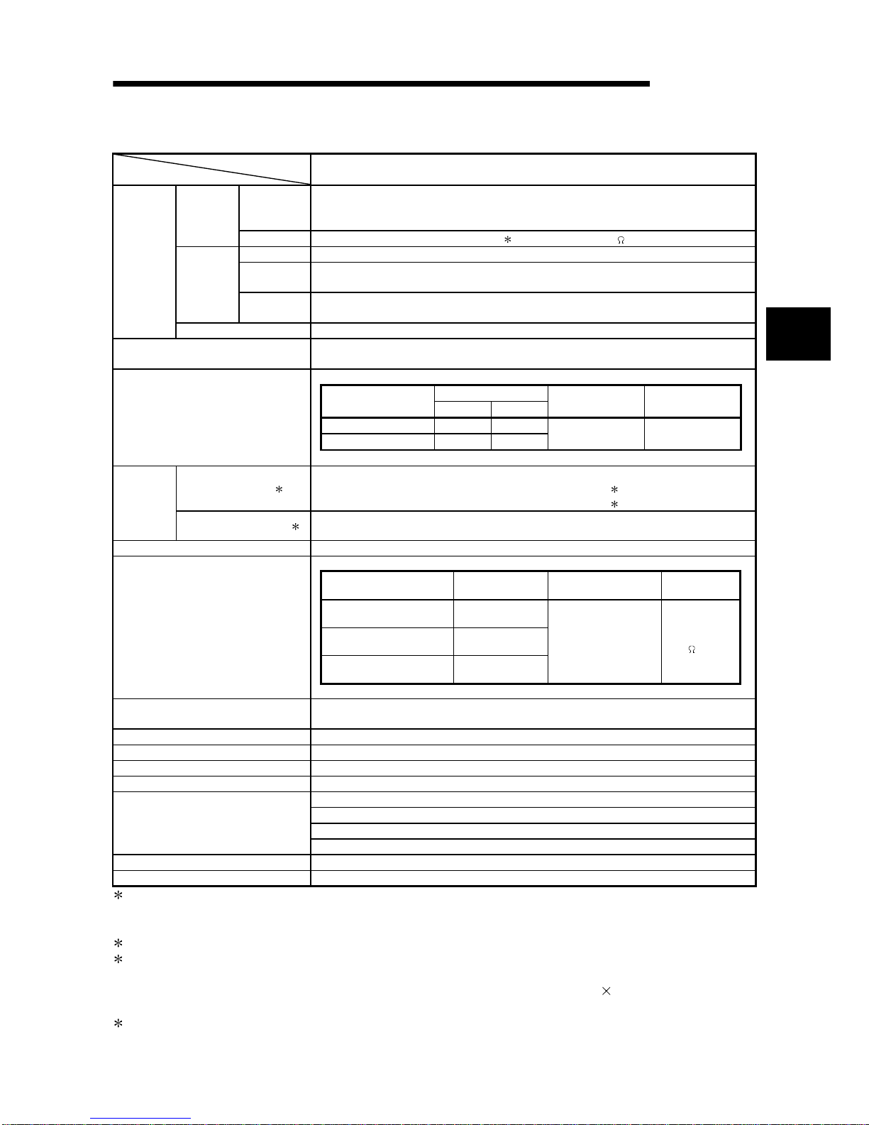
Channel Isolated High Resolution Analog-Digital Converter Module
Channel Isolated High Resolution Analog-Digital Converter Module
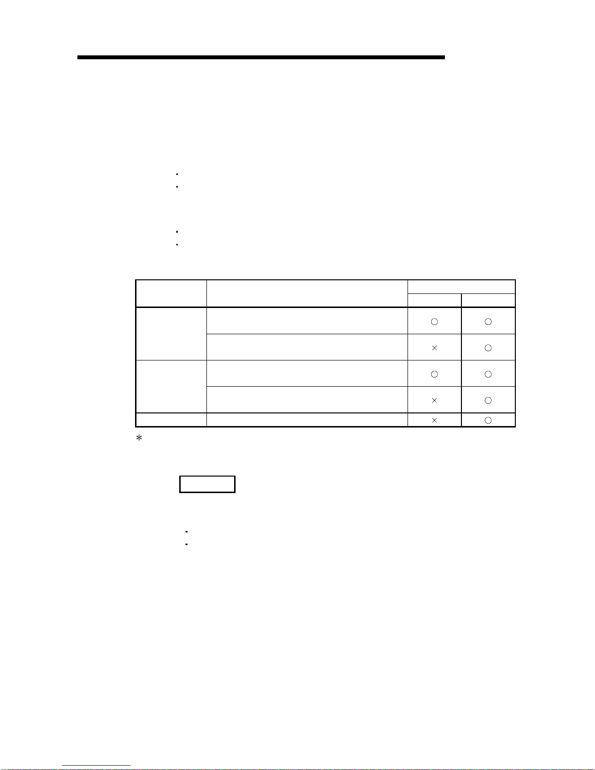
U
Channel Isolated High Resolution Analog-Digital Converter Module Channel Isolated High Resolution Analog-Digital Converter Module (With Signal Conditioning Function) User's Manual
(With Signal Conditioning Function)
Mitsubishi Programmable
Logic Controller
Q64AD-GH
Q62AD-DGH
GX Configurator-AD
(SW2D5C-QADU-E)

A - 1 A - 1
• SAFETY PRECAUTIONS •
(Always read these instructions before using this equipment.)
Before using this product, please read this manual and the relevant manuals introduced in this manual
carefully and pay full attention to safety to handle the product correctly.
The instructions given in this manual are concerned with this product. For the safety instructions of the
PLC system, please read the user's manual for the CPU module to use.
In this manual, the safety instructions are ranked as "DANGER" and "CAUTION".
!
DANGER
CAUTION
!
Indicates that incorrect handling may cause hazardous conditions,
resulting in death or severe injury.
Indicates that incorrect handling may cause hazardous conditions,
resulting in medium or slight personal injury or physical damage.
Note that the !CAUTION level may lead to a serious consequence according to the circumstances.
Always follow the instructions of both levels because they are important to personal safety.
Please store this manual in a safe place and make it accessible when required. Always forward it to the
end user.
[DESIGN PRECAUTION]
!
DANGER
• Do not write data into the "system area" of the buffer memory of intelligent function modules.
Also, do not use any "prohibited to use" signals as an output signal to an intelligent function
module from the PLC CPU.
Writing data into the "system area" or outputting a signal for "prohibited to use" may cause a
PLC system malfunction.
!
CAUTION
• Do not bunch the control wires or communication cables with the main circuit or power wires, or
install them close to each other.
They should be installed 100mm(3.9inch) or more from each other.
Not doing so could result in noise that may cause malfunction.

A - 2 A - 2
[INSTALLATION PRECAUTIONS]
!
CAUTION
• Use the PLC in an environment that meets the general specifications contained in the user's
manual of the CPU module to use.
Using this PLC in an environment outside the range of the general specifications may cause
electric shock, fire, malfunction, and damage to or deterioration of the product.
• While pressing the installation lever located at the bottom of module, insert the module fixing tab
into the fixing hole in the base unit until it stops. Then, securely mount the module with the fixing
hole as a supporting point.
Improper installation may result in malfunction, breakdown or the module coming loose and
dropping.
Securely fix the module with screws if it is subject to vibration during use.
• Tighten the screws within the range of specified torque.
If the screws are loose, it may cause the module to fallout, short circuits, or malfunction.
If the screws are tightened too much, it may cause damage to the screw and/or the module,
resulting in fallout, short circuits or malfunction.
• Be sure to shut off all phases of the external power supply used by the system before mounting
or removing the module.
Not doing so may cause damage to the module.
In the system where a CPU module supporting the online module change is used and on the
MELSECNET/H remote I/O stations, modules can be replaced online (during energizing).
However, there are some restrictions on replaceable modules and the replacement procedures
are predetermined for each module.
For details, refer to the chapter of the online module change in this manual.
• Do not directly touch the conductive area or electronic components of the module.
Doing so may cause malfunction or failure in the module.
[WIRING PRECAUTIONS]
!
CAUTION
• Always ground the FG terminal of the Q62AD-DGH.
Not doing so can cause an electric shock or malfunction.
• When turning on the power and operating the module after wiring is completed, always attach
the terminal cover that comes with the product.
There is a risk of electric shock if the terminal cover is not attached.
• Use applicable solderless terminals and tighten them with the specified torque.If any solderless
spade terminal is used, it may be disconnected when the terminal screw comes loose, resulting
in failure.
• Tighten the terminal screws within the range of specified torque.
If the terminal screws are loose, it may result in short circuits or malfunction.
If the terminal screws are tightened too much, it may cause damage to the screw and/or the
module, resulting in short circuits or malfunction.
• Be careful not to let foreign matter such as sawdust or wire chips get inside the module.
They may cause fires, failure or malfunction.
• The top surface of the module is covered with protective film to prevent foreign objects such as
cable offcuts from entering the module when wiring.
Do not remove this film until the wiring is complete.
Before operating the system, be sure to remove the film to provide adequate ventilation.

A - 3 A - 3
[STARTING AND MAINTENANCE PRECAUTIONS]
!
CAUTION
• Do not disassemble or modify the modules.
Doing so could cause failure, malfunction injury or fire.
• Be sure to shut off all phases of the external power supply used by the system before mounting
or removing the module.
Not doing so may cause failure or malfunction of the module.
In the system where a CPU module supporting the online module change is used and on the
MELSECNET/H remote I/O stations, modules can be replaced online (during energizing).
However, there are some restrictions on replaceable modules and the replacement procedures
are predetermined for each module.
For details, refer to the chapter of the online module change in this manual.
• Do not mount/remove the module onto/from the base unit more than 50 times (IEC 61131-2compliant), after the first use of the product.
Failure to do so may cause malfunction.
• Do not touch the connector while the power is on.
Doing so may cause malfunction.
• Be sure to shut off all phases of the external power supply before cleaning or retightening the
terminal screws or module fixing screws.
Not doing so may cause failure or malfunction of the module.
If the screws are loose, it may cause the module to fallout, short circuits, or malfunction.
If the screws are tightened too much, it may cause damages to the screws and/or the module,
resulting in the module falling out, short circuits or malfunction.
• Always make sure to touch the grounded metal to discharge the electricity charged in the body,
etc., before touching the module.
Failure to do so may cause a failure or malfunctions of the module.
[DISPOSAL PRECAUTIONS]
!
CAUTION
• When disposing of this product, treat it as industrial waste.
A - 4 A - 4
REVISIONS
The manual number is given on the bottom left of the back cover.
Print Date Manual Number Revision
May, 2002 SH (NA)-080277-A First edition
Feb., 2003 SH (NA)-080277-B
Correction
SAFETY PRECAUTIONS, Section 2.1, 3.4.1, 3.4.23, 4.4.2, 5.1, 5.5.2,
5.6.1, 5.6.3, 6.3.2, 6.5.2, 7.3.4, 7.3.6, 7.4, Appendix 1.2, Appendix 1.3
May, 2003 SH (NA)-080277-C
Addition
Section 2.3
Correction
Section 2.2, 3.4.1, 3.4.22, 3.4.23, 4.5, 4.6, 4.6.1, 4.6.2, 5.3.1
May, 2004 SH (NA)-080277-D
Correction
Section 2.2, 2.3, 3.1.1, 3.1.3, 3.2.1, 7.1, 7.3.1 to 7.3.6, 8.2.6
Aug., 2004 SH (NA)-080277-E
Addition
Section 5.6.3, 5.7, 5.8
Correction
Section 1.1, 5.1, 5.2.1, 5.2.2, 5.3.1, 5.3.2, 5.3.3, 5.6.1, 5.6.2,
Appendix 1.3
Oct., 2004 SH (NA)-080277-F
Correction
SAFETY PRECAUTIONS, Section 2.1, 3.1.1, 4.1, 6.3, 6.5.1
Sep., 2005 SH (NA)-080277-G
Correction
SAFETY PRECAUTIONS, Section 2.1, 3.1.1, 5.2.2, 6.3.2
Feb., 2006 SH (NA)-080277-H
Correction
Section 2.2, 6.2.1, 6.2.2, 6.3.1, 6.3.2, 6.4.1, 6.4.2, 6.5.1, 6.5.2,
Appendix1
Japanese Manual Version SH-080262-I
This manual confers no industrial property rights or any rights of any other kind, nor does it confer any patent
licenses. Mitsubishi Electric Corporation cannot be held responsible for any problems involving industrial property
rights which may occur as a result of using the contents noted in this manual.
© 2002 MITSUBISHI ELECTRIC CORPORATION

A - 5 A - 5
INTRODUCTION
Thank you for purchasing the MELSEC-Q series PLC.
Before using the equipment, please read this manual carefully to develop full familiarity with the functions
and performance of the Q series PLC you have purchased, so as to ensure correct use.
Please forward a copy of this manual to the end user.
CONTENTS
SAFETY PRECAUTIONS..............................................................................................................................A- 1
REVISIONS ....................................................................................................................................................A- 4
INTRODUCTION............................................................................................................................................A- 5
CONTENTS....................................................................................................................................................A- 5
About Manuals ...............................................................................................................................................A- 9
Conformation to the EMC Directive and Low Voltage Instruction ................................................................A-10
About the Generic Terms and Abbreviations ................................................................................................A-11
Product Structure ...........................................................................................................................................A-12
1 OVERVIEW 1- 1 to 1- 3
1.1 Features .................................................................................................................................................. 1- 1
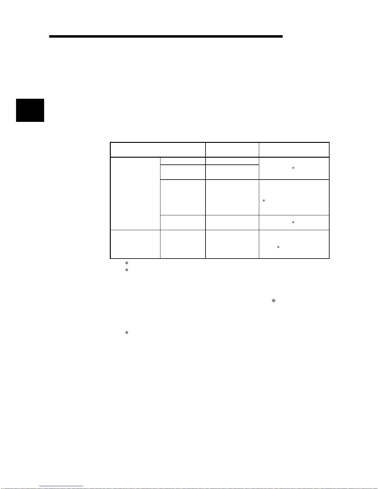
2 SYSTEM CONFIGURATION 2- 1 to 2- 6
2.1 Applicable Systems................................................................................................................................. 2- 1
2.2 How to Check the Function Version, Serial Number, Product Information and Software Version ...... 2- 3
2.3 Cautions for Power Supply from Q61P-A1/A2 to Q64AD-GH............................................................... 2- 5
3 SPECIFICATIONS 3- 1 to 3-49
3.1 Performance Specifications .................................................................................................................... 3- 1
3.1.1 Performance specifications list ........................................................................................................ 3- 1
3.1.2 I/O conversion characteristic............................................................................................................ 3- 4
3.1.3 Accuracy........................................................................................................................................... 3- 9
3.2 Function List ............................................................................................................................................ 3-10
3.2.1 A/D conversion methods .................................................................................................................. 3-11
3.2.2 Maximum and minimum values hold function .................................................................................3-13
3.2.3 Input signal error detection function ................................................................................................ 3-13
3.2.4 Warning output function ...................................................................................................................3-14
3.2.5 A/D conversion starting time setting function (Q62AD-DGH only) ................................................. 3-18
3.3 I/O Signals for the PLC CPU .................................................................................................................. 3-19
3.3.1 List of I/O signals .............................................................................................................................. 3-19
3.3.2 Details of I/O signals ........................................................................................................................ 3-21
3.4 Buffer Memory......................................................................................................................................... 3-28
3.4.1 Buffer memory assignment.............................................................................................................. 3-28
3.4.2 A/D conversion enable/disable setting (buffer memory address 0: Un\G0) ................................... 3-36
3.4.3 CH
Average time/Average number of times/Move average/Time constant settings
(buffer memory addresses 1 to 4: Un\G1 to Un\G4)....................................................................... 3-37
3.4.4 CH
A/D conversion starting time setting
(buffer memory addresses 5, 6: Un\G5, Un\G6) (Q62AD-DGH only) ............................................ 3-37

A - 6 A - 6
3.4.5 Averaging process specification (buffer memory address 9: Un\G9)............................................. 3-38
3.4.6 A/D conversion completed flag (buffer memory address 10: Un\G10) .......................................... 3-39
3.4.7 CH
digital output value (16bit) (buffer memory addresses 11 to 14: Un\G11 to Un\G14).......... 3-39
3.4.8 Write data error codes (buffer memory address 19: Un\G19) ........................................................ 3-40
3.4.9 Setting range (buffer memory address 20: Un\G20)....................................................................... 3-40
3.4.10 Offset/gain setting mode (buffer memory addresses 22, 23: Un\G22, Un\G23) ......................... 3-41
3.4.11 CH
maximum value/minimum value storage area (16bit)
(buffer memory addresses 30 to 37: Un\G30 to Un\G37) ............................................................ 3-41
3.4.12 Input signal error detection/warning output settings (buffer memory address 47: Un\G47)........ 3-42
3.4.13 Warning output flag (buffer memory address 48 :Un\G48) .......................................................... 3-42
3.4.14 Input signal error detection flag (buffer memory address 49: Un\G49)........................................ 3-43
3.4.15 CH
digital output value (32bit) (buffer memory addresses 54 to 61: Un\G54 to Un\G61)........ 3-43
3.4.16 CH
maximum value/minimum value storage area (32bit)
(buffer memory addresses 62 to 77: Un\G62 to Un\G77) ............................................................ 3-44
3.4.17 CH
process alarm upper/lower limit value
(buffer memory addresses 86 to 117: Un\G86 to Un\G117) ........................................................ 3-44
3.4.18 CH
rate alarm warning detection period
(buffer memory addresses 118 to 121: Un\G118 to Un\G121) ....................................................3-45
3.4.19 CH
rate alarm upper/lower limit value
(buffer memory addresses 122 to 137: Un\G122 to Un\G137) ....................................................3-46
3.4.20 CH
input signal error detection setting value
(buffer memory addresses 138 to 141: Un\G138 to Un\G141) ....................................................3-47
3.4.21 Mode switching setting (buffer memory addresses 158, 159: Un\G158, Un\G159).................... 3-48
3.4.22 Pass data classification setting (buffer memory addresses 200: Un\G200) (Q64AD-GH only) .. 3-48
3.4.23 Industrial shipment settings and user range settings offset/gain value
(buffer memory addresses 202 to 233: Un\G202 to Un\G233) ....................................................3-49
4 SETUP AND PROCEDURES BEFORE OPERATION 4- 1 to 4-17
4.1 Handling Precautions .............................................................................................................................. 4- 1
4.2 Setup and Procedures before Operation ............................................................................................... 4- 2
4.3 Part Identification Nomenclature ............................................................................................................ 4- 3
4.4 Wiring....................................................................................................................................................... 4- 5
4.4.1 Wiring precautions............................................................................................................................ 4- 5
4.4.2 External wiring .................................................................................................................................. 4- 6
4.5 Switch Setting for Intelligent Function Module ....................................................................................... 4- 8
4.6 Offset/Gain Settings ................................................................................................................................ 4-10
4.6.1 Offset/Gain Settings (Q64AD-GH)................................................................................................... 4-10
4.6.2 Offset/Gain Settings (Q62AD-DGH) ................................................................................................ 4-14
4.6.3 A/D conversion value storage during offset/gain setting................................................................. 4-17
5 UTILITY PACKAGE (GX Configurator-AD) 5- 1 to 5-31
5.1 Utility Package Functions........................................................................................................................ 5- 1
5.2 Installing and Uninstalling the Utility Package........................................................................................ 5- 2
5.2.1 User precautions ..............................................................................................................................5- 2
5.2.2 Operating environment..................................................................................................................... 5- 4

A - 7 A - 7
5.3 Explanation of Utility Package Operation ............................................................................................... 5- 5
5.3.1 How to perform common utility package operations ....................................................................... 5- 5
5.3.2 Operation overview .......................................................................................................................... 5- 8
5.3.3 Starting the intelligent function module utility ..................................................................................5-10
5.4 Initial Setting ............................................................................................................................................ 5-13
5.5 Automatic Refresh Setting ...................................................................................................................... 5-15
5.6 Monitor/Test ............................................................................................................................................ 5-17
5.6.1 Monitor/test screen........................................................................................................................... 5-17
5.6.2 Offset/gain setting operation ............................................................................................................ 5-20
5.6.3 Confirmation of Conversion Characteristic....................................................................................... 5-21
5.6.4 Pass data (Q64AD-GH) ....................................................................................................................5-23
5.6.5 Pass data (Q62AD-DGH).................................................................................................................. 5-25
5.7 FB Conversion of Initial Setting/Auto Refresh Setting ............................................................................5-26
5.8 Usage of FB ............................................................................................................................................. 5-27
5.8.1 Outline................................................................................................................................................ 5-27
5.8.2 Paste an FB to a Sequence Program............................................................................................... 5-29
5.8.3 Convert (Compile) a Sequence Program ......................................................................................... 5-30
6 PROGRAMMING 6- 1 to 6-25
6.1 Programming Procedure......................................................................................................................... 6- 1
6.2 For Use in Normal System Configuration (Q64AD-GH) ........................................................................ 6- 2
6.2.1 Programming Example Using the Utility Package .......................................................................... 6- 3
6.2.2 Programming Example without Using the Utility Package.............................................................. 6- 5
6.3 For Use in Remote I/O Network (Q64AD-GH) ....................................................................................... 6- 7
6.3.1 Programming Example Using the Utility Package .......................................................................... 6- 9
6.3.2 Programming Example without Using the Utility Package.............................................................. 6-12
6.4 For Use in Normal System Configuration (Q62AD-DGH) ..................................................................... 6-15
6.4.1 Programming Example Using the Utility Package .......................................................................... 6-16
6.4.2 Programming Example without Using the Utility Package.............................................................. 6-18
6.5 For Use in Remote I/O Network (Q62AD-DGH) ....................................................................................6-19
6.5.1 Programming Example Using the Utility Package .......................................................................... 6-20
6.5.2 Programming Example without Using the Utility Package.............................................................. 6-22
7 ONLINE MODULE CHANGE 7- 1 to 7-36
7.1 Online Module Change Conditions......................................................................................................... 7- 2
7.2 Online Module Change Operations ........................................................................................................ 7- 3
7.3 Online Module Change Procedure ......................................................................................................... 7- 4
7.3.1 When industrial shipment setting is used and initial setting was made with
GX Configurator-AD ......................................................................................................................... 7- 4
7.3.2 When industrial shipment setting is used and initial setting was made with sequence program .. 7- 9
7.3.3 When user range setting is used and initial setting was made with GX Configurator-AD
(other system is available) ............................................................................................................... 7-14
7.3.4 When user range setting is used and initial setting was made with GX Configurator-AD
(other system is unavailable) ........................................................................................................... 7-19
7.3.5 When user range setting is used and initial setting was made with sequence program
(other system is available) ............................................................................................................... 7-25

A - 8 A - 8
7.3.6 When user range setting is used and initial setting was made with sequence program
(other system is unavailable) ........................................................................................................... 7-30
7.4 Range Reference Table.......................................................................................................................... 7-35
7.5 Precautions for Online Module Change .................................................................................................7-36
8 TROUBLESHOOTING 8- 1 to 8- 6
8.1 Error Code List ........................................................................................................................................ 8- 1
8.2 Troubleshooting ...................................................................................................................................... 8- 3
8.2.1 When the "RUN" LED is flashing or turned off................................................................................ 8- 3
8.2.2 When the "ERR." LED is on or flashing........................................................................................... 8- 3
8.2.3 When the "ALM" LED is on or flashing ............................................................................................ 8- 3
8.2.4 When the digital output values cannot be read............................................................................... 8- 4
8.2.5 When A/D conversion completed flag does not turn ON during use in normal mode ................... 8- 5
8.2.6 Checking the A/D converter module status using GX Developer system monitor ........................ 8- 5
APPENDIX App.- 1 to App.-14
Appendix 1 Dedicated Instruction List and Available Devices................................................................App.- 1
Appendix 1.1 OFFGAN ........................................................................................................................App.- 2
Appendix 1.2 OGLOAD........................................................................................................................App.- 4
Appendix 1.3 OGSTOR........................................................................................................................App.- 8
Appendix 2 Performance Comparison between Q64AD-GH and Q64AD .............................................App.-13
Appendix 3 External Dimensions.............................................................................................................App.-14
INDEX Index- 1 to Index- 3

A - 9 A - 9
About Manuals
The following manuals are also related to this product.
If necessary, order them by quoting the details in the tables below.
Related Manuals
Manual Name
Manual Number
(Model Code)
GX Developer Version 8 Operating Manual
Describes the methods of using GX Developer to create a program and print out, monitor, and debug
the program. (Sold separately)
SH-080373E
(13JU41)
GX Developer Version 8 Operating Manual (Function Block)
Describes the methods of using GX Developer to create a function block and print out the function
block. (Sold separately)
SH-080376E
(13JU44)
REMARK
If you would like to obtain a manual individually, printed matters are available
separately. Order the manual by quoting the manual number on the table above
(model code).

A - 10 A - 10
Conformation to the EMC Directive and Low Voltage Instruction
When incorporating the Mitsubishi PLC into other machinery or equipment and
keeping compliance with the EMC and low voltage directives, refer to Chapter 3,
"EMC Directives and Low Voltage Directives" of the User's Manual (Hardware)
included with the CPU module or base unit used.
The CE logo is printed on the rating plate on the main body of the PLC that conforms
to the EMC directive and low voltage instruction.
By making this product conform to the EMC directive and low voltage instruction, it is
not necessary to make those steps individually.
A - 11 A - 11
About the Generic Terms and Abbreviations
Unless otherwise specified, this manual uses the following general terms and
abbreviations.
Abbreviation/general terms Description of the abbreviation/general terms
A/D converter module Generic term for Q64AD-GH and Q62AD-DGH
DOS/V personal computer IBM PC/AT® or compatible computer with DOS/V.
GX Developer
Generic product name of the product types SWnD5C-GPPW-E, SWnD5C-GPPW-EA,
SWnD5C-GPPW-EV and SWnD5C-GPPW-EVA.
"n" in the model name is 4 or greater.
GX Configurator-AD
Generic term for analog-digital converter module setting and monitor tool GX
Configurator-AD (SW2D5C-QADU-E)
QCPU (Q mode)
Generic term for Q00JCPU, Q00CPU, Q01CPU, Q02CPU, Q02HCPU, Q06HCPU,
Q12HCPU, Q25HCPU, Q12PHCPU, Q25PHCPU
QnPHCPU Generic term for Q12PHCPU and Q25PHCPU.
Personal computer Generic term for DOS/V personal computer
Industrial shipment setting
Generic term for analog input ranges 0 to 10V, 0 to 5V, 1 to 5V, -10 to 10V, 0 to 20mA
and 4 to 20mA
FB Abbreviation of function block.
A - 12 A - 12
Product Structure
The product structure of this product is given in the table below.
Model code Product name Quantity
Q64AD-GH
Type Q64AD-GH Channel Isolated High Resolution Analog-Digital
Converter Module
1
Q62AD-DGH
Type Q62AD-DGH Channel Isolated High Resolution Analog-Digital
Converter Module (with Signal Conditioning Function)
1
SW2D5C-QADU-E GX Configurator-AD Version 2 (1-license product) (CD-ROM) 1
SW2D5C-QADU-EA GX Configurator-AD Version 2 (Multiple-license product) (CD-ROM) 1

1 - 1 1 - 1
MELSEC-Q
1 OVERVIEW
1 OVERVIEW
This User's Manual describes the specifications, handling and programming methods
for the type Q64A D -GH cha nn el isola t ed high re so lution analog-digital converter
module (hereinafter referred to as the Q64AD-GH) and type Q62AD-DGH channel
isolated high resol ut io n an al og -dig it al conv e rte r modu le (w ith sign al cond it io nin g
function) (hereinafter referred to as the Q62AD-DGH), which are used with the
MELSEC-Q series CPU modules.
The Q62AD-DGH is exclusively used for current input.
In this manual, the Q64AD-GH and Q62AD-DGH are collectively referred to as the A/D
converter modules.
1.1 Features
(1) Channel isolated
The channels are isolated.
The Q62AD-DGH is also isolated between the external supply power and
channels.
(2) High resolution
The resolution is as high as 32-bit signed binary (data part is 16 bits long). (When
the -10V to +10V range is selected)
(3) Power supply to 2-wire tr ansmitter ( Q62AD- D GH only)
Supplying power to the 2-wire transmitter, the Q62AD-DGH does not require the
power supply for the 2-wire transmitter.
Supply power can be switched ON/OFF channel-by-channel by the A/D
conversion enable/disable setting.
(4) Module protection provided by shor t-circ uit pr otecti on cir cui t
(Q62AD-DGH only)
If an excessive current flows into the module due to a short circuit of the wiring,
the short-circuit protection circuit limits the current to within 25 to 35mA,
protecting the module.
(5) Analog input check by check terminals (Q62AD-D GH only)
Measurement of a voltage at the check terminals allows the mA of the 2-wire
transmitter output to be checked without the wiring being disconnected.
(6) High accuracy
The reference accuracy 1 is as high as ±0.05% and the temperature coefficient
2
is as high as ±71. 4pp m/°C .
1 Accuracy of offset/gain setting at ambient temperature
2 Accuracy per temperature change of 1°C
Example) Accuracy when the temperature varies from 25°C to 30°C
0.05% (reference accuracy) + 0.00714%/°C (temperature
coefficient)
5°C (temperatu re va ri a tio n di ffe re n ce ) = 0. 0 857%
1

1 - 2 1 - 2
MELSEC-Q
1 OVERVIEW
(7) Changing the input range
The input range 3 ca n ea sily be set fro m th e GX De vel o pe r.
3 Input range refers to the type of offset/gain settings. The most frequently
used range is set as the default but the user can also set the offset/gain.
(8) A/D conversion system
There are the following five A/D conversion systems.
(a) Sampling processing
Analog input values are converted into digital values one by one on a
channel basis and the digital output value is output at every conversion.
(b) Averaging processing
1) Time averaging
A/D conversion is averaged in terms of time on a channel basis and a
digital average value is output.
2) Count averaging
A/D conversion is averaged in terms of count on a channel basis and a
digital average value is output.
3) Move averaging
The specified number of digital output values measured per sampling
time are averaged .
(c) Primary delay filter
A digital output value is smoothed according to the preset time constant.
(9) Input signal error detection function
The voltage/cur ren t out sid e th e set ting ra nge is detected.
(10) Warning output
There are the following two warning outputs.
(a) Process alarm
A warning is output if a digital output value falls outside the setting range.
(b) Rate alarm
A warning is output if the varying rate of a digital output value falls outside
the preset varying rate range.
(11) Online module change
The module can be changed without the system being stopped.
Further, the dedicated instruction (G. OGLOAD, G. OGSTOR), write to the buffer
memory, or turning ON the Y signal enables "inheritance of offset/gain settings to
the new A/D conve rt er mod ule repl a ci ng th e old one changed online" and
"transfer of offset/gain settings to the other A/D converter module mounted on the
other slot". (These apply to the modules of the same model.)
1

1 - 3 1 - 3
MELSEC-Q
1 OVERVIEW
(12) Offset/gain setting
GX Configurator-AD, dedicated instruction (G. OFFGAN) or mode switching
setting allows a shift to the offset/gain setting mode easily.
(13) Easy settings using the utility package
A utility package is sold separately (GX Configurator-AD).
The utility package is not a required item, however, it is useful for on-screen
setting of the intelligent function module parameters (initial setting/auto refresh
setting). In addition, FB
1
can be generated au to matically from the intelligent
function module parameters that have been set up and used in a sequence
program.
1: FB is the function for making a circuit block used in a sequence program
repeatedly a part (FB) to use it in the sequence program.
This function can improve the efficiency of program development and
minimize program bugs to improve program qualities.
For the details of FB, refer to "GX Developer Version 8 Operating Manual
(Function Block)."
2 - 1 2 - 1
MELSEC-Q
2 SYSTEM CONFIGURATION
2 SYSTEM CONFIGURATION
2.1 Applicable Systems
This section describes the system configuration for the A/D converter module.
(1) Applicable module and the number of modules that can be installed
The following are the CPU module and network module (for remote I/O stations)
in which the A/D converter module can be installed and the number of modules
that can be installed.
Applicable module
Number of modules that
can be installed
Remarks
Q00JCPU Maximum 16
Q00CPU
Q01CPU
Maximum 24
(
1
)
Q02CPU
Q02HCPU
Q06HCPU
Q12HCPU
Q25HCPU
Maximum 64
Can be installed in Q mode only
(
1
)
CPU module
Q12PHCPU
Q25PHCPU
Maximum 64
(
1
)
Network module
QJ72LP25-25
QJ72LP25G
QJ72LP25GE
QJ72BR15
Maximum 64
MELSECNET/H Remote I/O
station (
2
)
1 See User's Manual (Function Explanation, Program Fundamentals) for the CPU module to use.
2 See Q Corresponding MELSECNET/H Network System Reference Manual (Remote I/O
network).
(2) Base Unit in which the converter module can be installed
The A/D converter module can be installed in any I/O slot ( 3) of the base unit.
However, a power shortage may occur depending on the combination with other
installed modules and the number of modules used, so always take into
consideration the power supply capacity when installing modules.
3 Limited to the range of the number of I/O points in the CPU module and network module (for
remote I/O stations).
(3) Compatibility with a multiple PLC system
First read the QCPU user's manual (Function Explanation, Program
Fundamentals) if the A/D converter module is used with a multiple PLC system.
(a) Compatible A/D converter module
Use an A/D converter module with function version B or higher if using the
module in a multiple PLC system.
(b) Intelligent function module parameters
Perform PLC write of the intelligent function module parameters to the
control PLC of the A/D converter module only.
2
2 - 2 2 - 2
MELSEC-Q
2 SYSTEM CONFIGURATION
(4) Compatibility with online module change
To make an online module change, use the A/D converter module of function
version C or later.
POINT
The A/D converter module does not have the products of function versions A and B.
The products of function version C include the functions of the products of function
versions A and B.
(5) Q64AD-GH compatible software packages
The following table indicates the compatibility of the systems using the Q64ADGH with the software packages.
GX Developer is required when the Q64AD-GH is used.
Software Version
GX Developer
GX Configurator-AD
4
Single PLC system Version 7 or later
Q00J/Q00/Q01CPU
Multiple PLC system Version 8 or later
Single PLC system Version 4 or later
Q02/Q02H/Q06H/
Q12H/Q25HCPU
Multiple PLC system Version 6 or later
Single PLC system
Q12PH/Q25PHCPU
Multiple PLC system
Version 7.10L or later
If installed in a MELSECNET/H remote I/O
station
Version 6 or later
Version 1.14Q or later
4 When using the pass data, use the product of Version 1.16S or later.
(6) Q62AD-DGH compatible software packages
The following table indicates the compatibility of the systems using the Q62ADDGH with the software packages.
GX Developer is required when the Q62AD-DGH is used.
Software Version
GX Developer
GX Configurator-AD
Single PLC system Version 7 or later
Q00J/Q00/Q01CPU
Multiple PLC system Version 8 or later
Single PLC system Version 4 or later
Q02/Q02H/Q06H/
Q12H/Q25HCPU
Multiple PLC system Version 6 or later
Single PLC system
Q12PH/Q25PHCPU
Multiple PLC system
Version 7.10L or later
If installed in a MELSECNET/H remote I/O
station
Version 6 or later
Version 1.14Q or later
2
2 - 3 2 - 3
MELSEC-Q
2 SYSTEM CONFIGURATION
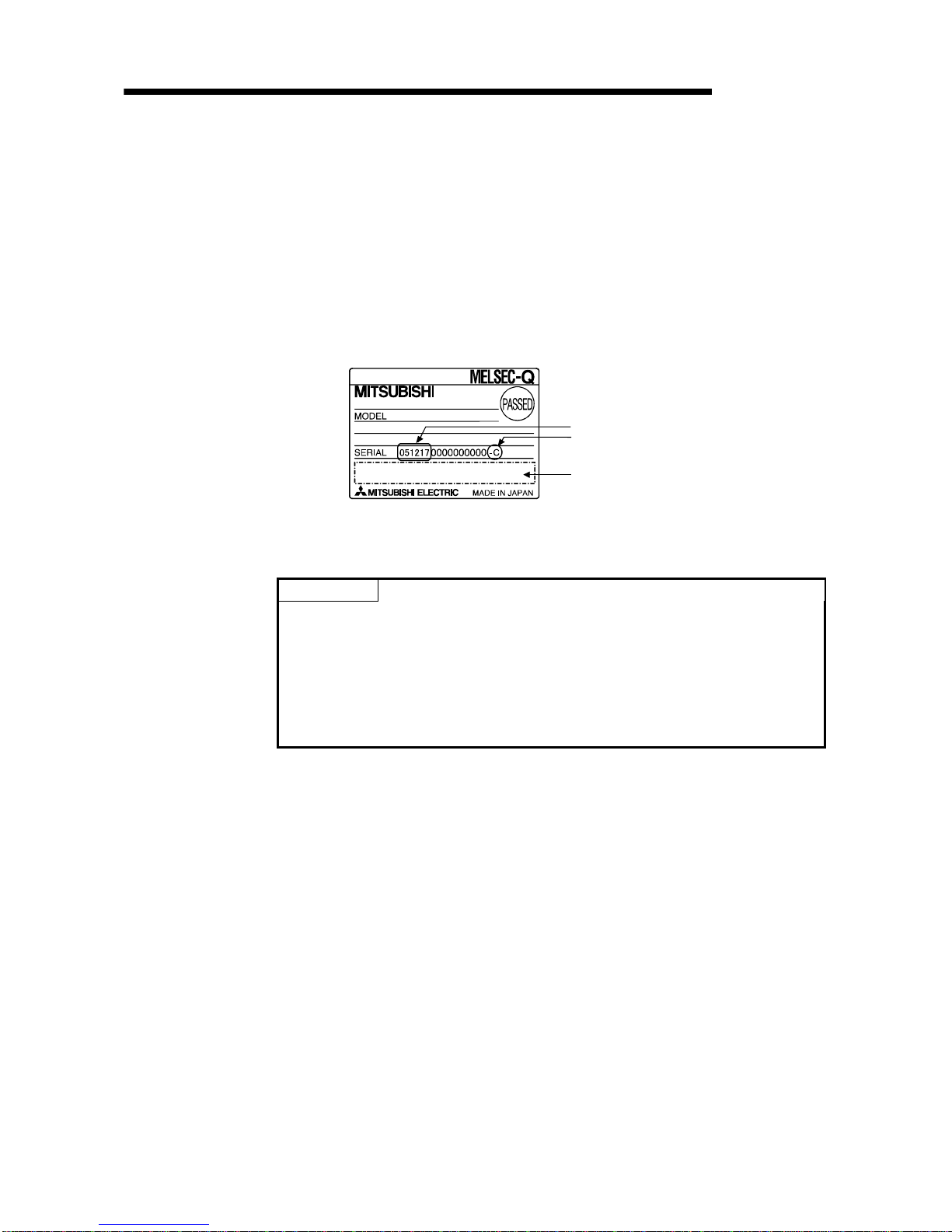
2.2 How to Check the Function Version, Serial Number, Product Information and Software
Version
This section describes how to check the function version, serial number, product
information of the A/D converter module and the software version of GX ConfiguratorAD.
(1) How to check the function version, serial number and product
information of the A/D converter module
(a) To check the function version and serial number using the "SERIAL column
of the rating plate" located on the side of the module
Function version
Conformed standard
Serial No. (First 6 digits)
(b) To check the function version and product information using GX Developer
Refer to Section 8.2.6 of this manual.
POINT
The serial No. described on the rated plate may not match with the serial No.
displayed on the product information of GX Developer.
• The serial No. on the rated plate describes the management information of the
product.
• The serial No. displayed on the product information of GX Developer describes
the function information of the product.
The function information of the product is updated when adding functions.
2 - 4 2 - 4
MELSEC-Q
2 SYSTEM CONFIGURATION
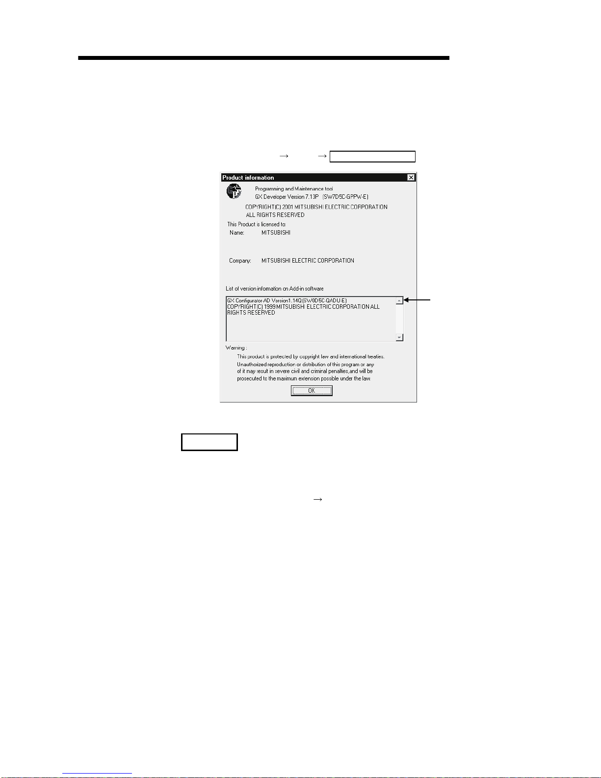
(2) How to check the GX Configurator-AD software version
The GX Configurator-AD software version can be checked in GX Developer's
"Product information" screen.
[Startup procedure]
GX Developer "Help" Product information
(In the case of GX Developer Version 7)
Software version
REMARK
The version indication for the GX Configurator-AD has been changed as shown
below from the SW0D5C-QADU-E 50F upgrade product.
Previous product Upgrade and subsequent versions
SW0D5C-QADU-E 50F
GX Configurator-AD Version 1.10L
2 - 5 2 - 5
MELSEC-Q
2 SYSTEM CONFIGURATION
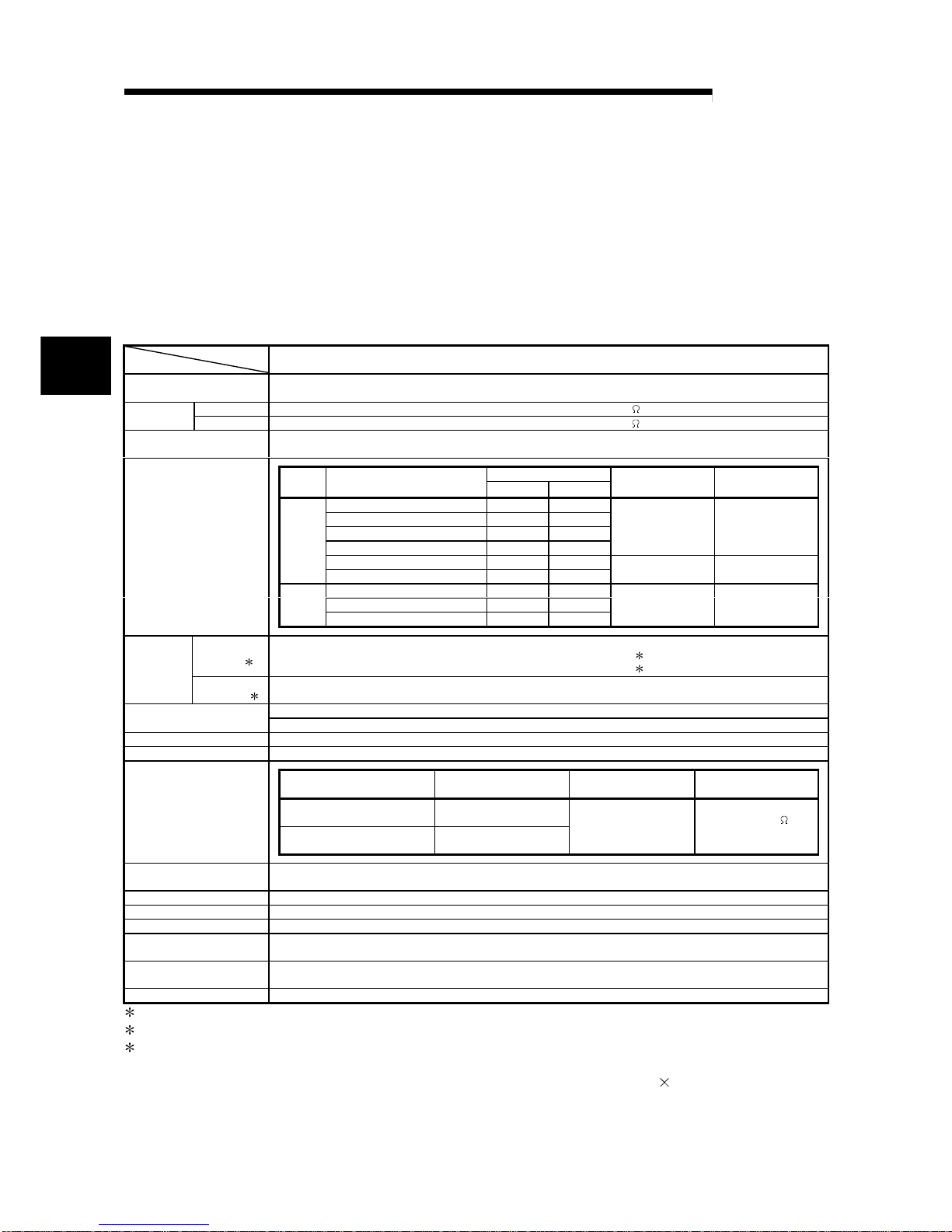
2.3 Cautions for Power Supply from Q61P-A1/A2 to Q64AD-GH
When using the Q61P-A1/A2 and Q64AD-GH in combination, it is required to use them
within the range in Table 2.1.
This requirement applies to the case where the Q64AD-GH satisfies any of the
following conditions.
The first six digits of serial number are "050914" or earlier.
The first five digits of "Product information" number are "05081" or earlier.
If it satisfies the above conditions but does not meet the ones outlined in Table 2.1,
carry out the following:
Replace the power supply module with the Q64P.
Mount the Q64AD-GH to another base unit.
Table 2.1 Conditions for Use of Q61P-A1/A2 and Q64AD-GH in Combination
Available power supply
No. of Q64AD-GH
modules
Conditions
Q61P-A1/A2 Q64P
Total current consumption of all modules on the same
base is 5.0A or less.
3 or less
Total current consumption of all modules on the same
base exceeds 5.0A.
Module other than the Q64AD-GH is not mounted on
the same base.
4
Module other than the Q64AD-GH is mounted on the
same base.
5 or more
—
If the modules are used outside the condition range given in Table 2.1, the "POWER" LED of
the power supply module may flicker and the PLC CPU system may not start.
REMARK
When the Q64AD-GH satisfies any of the following conditions, the above precaution
does not apply.
The first six digits of serial number are "051217" or later.
The first five digits of "Product information" number are "05082" or later.

2 - 6 2 - 6
MELSEC-Q
2 SYSTEM CONFIGURATION
MEMO
3 - 1 3 - 1
MELSEC-Q
3 SPECIFICATIONS
3 SPECIFICATIONS
The description of this chapter and later is based on the Q64AD-GH.
3.1 Performance Specifications
3.1.1 Performance specifications list
Table 3.1 shows the performance specifications of the A/D converter modules.
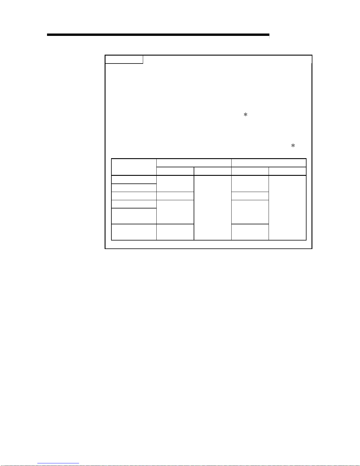
Table 3.1 Performance Specifications of Q64AD - GH
Model name
Item
Q64AD-GH
Number of analog input
points
4 points (4 channels)
Voltage -10 to 10VDC (Input resistance 1 M )
Analog input
Current 0 to 20mADC (Input resistance 250
)
Digital output
16-bit signed binary (-32768 to 32767)
32-bit signed binary (-65536 to 65535)
Maxi mum resolution
Input Analog input range
32-bit 16-bit
Digital output value
(32-bit)
Digital output value
(16-bit)
0 to 10V 156.3µV 312.6µV
0 to 5V 78.2µV 156.4µV
1 to 5V 62.5µV 125.0µV
Users input range (Uni-polar) 47.4µV 94.8µV
0 to 64000 0 to 32000
-10 to 10V 156.3µV 312.6µV
Voltage
Users input range (Bi-polar) 47.4µV 94.8µV
-64000 to 64000 -32000 to 32000
0 to 20mA 312.5nA 625.0nA
4 to 20mA 250.0nA 500.0nA
Current
Users input range (Uni-polar) 151.6nA 303.2nA
0 to 64000 0 to 32000
I/O characteristi cs ,
maximum resolution
Reference
accuracy
1
±0.05%
Digital output value (32-bit) : ±32digit
2
Digital output value (16-bit) : ±16digit
2
Accuracy
(Accuracy
relative to
digital output
value)
Temperature
coefficient
3
±71.4ppm/°C (0.00714%/°C)
Common mode voltage Input-Common ground (input voltage 0V): 1780VAC
Common mode
characteristic
Common mode voltage rejection ratio (VCM < 1780V): 60Hz 105dB, 50Hz 107dB
Conversion speed 10ms/4 channels
Absolute maximum input Voltage: ± 15V Current: ± 30mA
Specific isolated area Isolation method
Dielectric withstand
voltage
Insulation resistance
Between I/O terminal and
PLC power supply
Photocoupler isolation
Between analog input
channels
Transformer isolation
1780VAC rms/3 cycles
(elevation 2000m)
500VDC 10M
or
more
Isolation specifications
Maximum number of writes
for E
2
PROM
100,000
I/O occupied points 16 points (I/O assignment: Intelligent 16 points)
Connected terminal 18 points terminal block
Applicable wire size 0.3 to 0.75mm
2
Applicable solderless
terminals
R1.25-3 (Solderless terminals with sleeves are not applicable)
Internal current
consumption (5VDC)
0.89A
Weight 0.20kg
1: Accuracy of offset/gain setting at ambient temperature
2: "digit" indicates a digital output value.
3: Accuracy per temperature change of 1°C
Example) Accuracy when temperature changes from 25 to 30°C
0.05% (reference accuracy) + 0.00714 %/°C (temperature coefficient)
5°C (temperature
change difference) = 0.0857%
3
3 - 2 3 - 2
MELSEC-Q
3 SPECIFICATIONS
Table 3.2 Performance Specifications of Q62AD-DGH
Model name
Item
Q62AD-DGH
Number of
analog input
points
2 points (2 channels)
Input
specification
Analog input 4 to 20mADC
4(Input resistance 250 )
Supply voltage 26±2VDC
Maximum
supply current
24mADC
Supply
power
specification
Short-circuit
protection
Available
Limit current: 25 to 35mA
Connecting
with 2-wire
transmitter
Check terminals Available
Digital output
16-bit signed binary (-768 to 32767)
32-bit signed binary (-1536 to 65535)
Maximum resolution
Analog input range
32-bit 16-bit
Digital output value
(32-bit)
Digital output value
(16-bit)
4 to 20mA 250.0nA 500.0nA
Users range setting 151.6nA 303.2nA
0 to 64000 0 to 32000
I/O characteristics, Maximum resolution
Reference accuracy 1
±0.05%
Digital output value (32-bit): ±32digit
2
Digital output value (16-bit): ±16digit
2
Accuracy
(Accuracy
relative to
digital output
value)
Temperature coefficient
3 ±71.4ppm/°C (0.00714 %/°C)
Conversion speed 10ms/2 channels
Specific isolated area Isolation method
Dielectric withstand
voltage
Insulation
resistance
Between I/O terminal and
PLC power supply
Photocoupler
isolation
Between analog input
channels
Transformer
isolation
Between external supply
power and analog input
Transformer
isolation
1780VAC rms/3 cycles
(elevation 2000m)
500VDC
10M
or more
Isolation specifications
Maximum number of writes for
E
2
PROM
100,000
Number of I/O occupied points 16 points
Connected terminal 18 points terminal block
Applicable wire size 0.3 to 0.75mm
2
Applicable solderless terminals R1.25-3 (Solderless terminals with sleeves are not applicable)
24VDC +20%, -15%
Ripple, spike within 500mV
P-P
Inrush current : 5.5A, within 200µs
External supply power
0.19A
Internal current consumption (5VDC) 0.33A
Weight 0.19kg
1: Accuracy of offset/gain setting at ambient temperature
Q62AD-DGH needs to be powered on 30 minutes prior to operation for compliance to the specification
(accuracy).
2: "digit" indicates a digital output value.
3: Accuracy per temperature change of 1°C
Example) Accuracy when temperature changes from 25 to 30°C
0.05% (reference accuracy) + 0.00714 %/°C (temperature coefficient)
5°C (temperature
change difference) = 0.0857%
4: User range setting is 2 to 24mA.
3

3 - 3 3 - 3
MELSEC-Q
3 SPECIFICATIONS
REMARK
See the user’s manual for the CPU module being used for general specifications of
the A/D converter modules.

3 - 4 3 - 4
MELSEC-Q
3 SPECIFICATIONS
3.1.2 I/O conversion characteristic
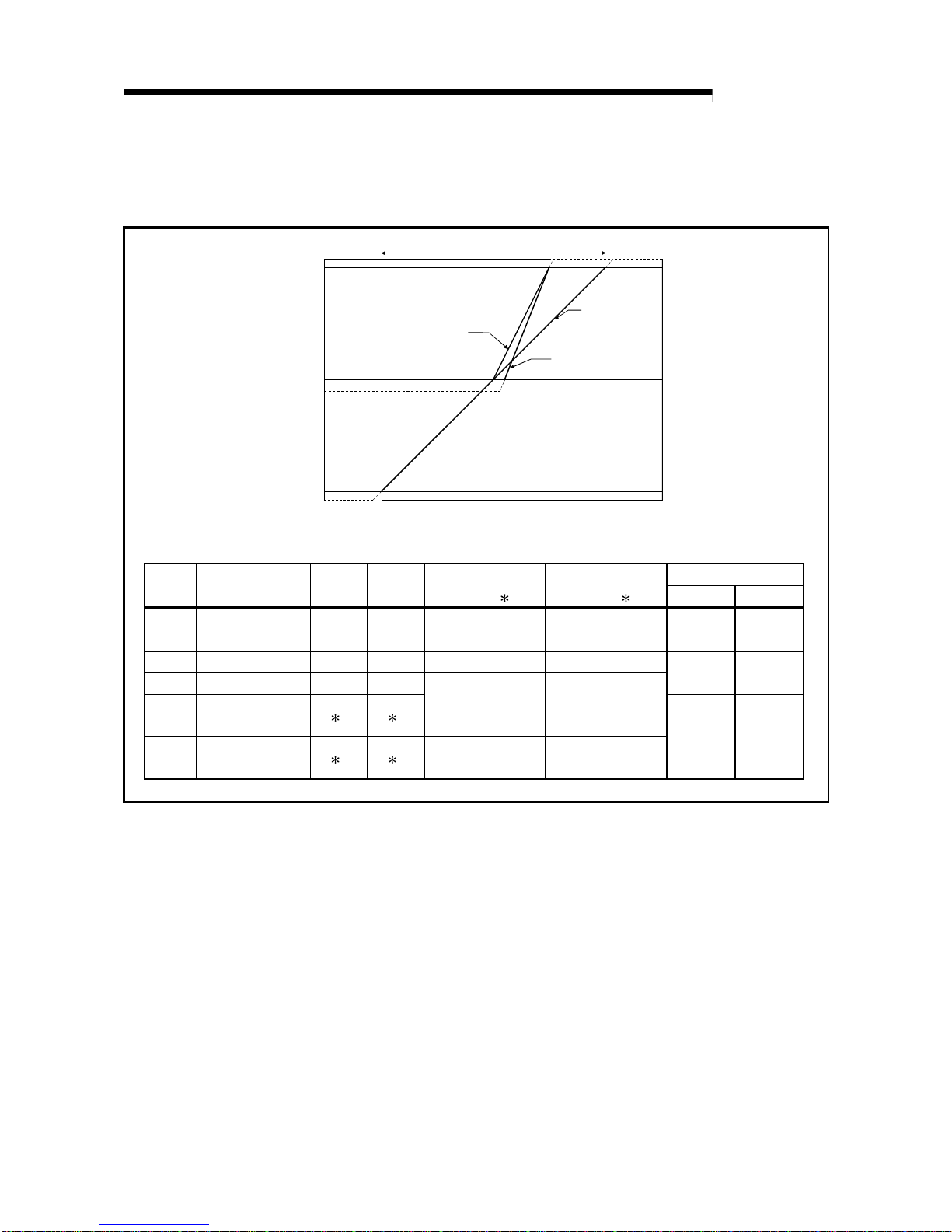
The I/O conversion characteristic represents the angle formed by a straight line
connecting the "offset value" and "gain value" when the analog signals (voltage or
current input) from outside the PLC are converted to digital values.
Offset value
The offset value denotes the analog input value (voltage or current) that makes the
digital output value 0.
Gain value
The gain value denotes the analog input value (voltage or current) that makes the
digital output value:
32000 (16 bits)
64000 (32 bits)
3 - 5 3 - 5
MELSEC-Q
3 SPECIFICATIONS
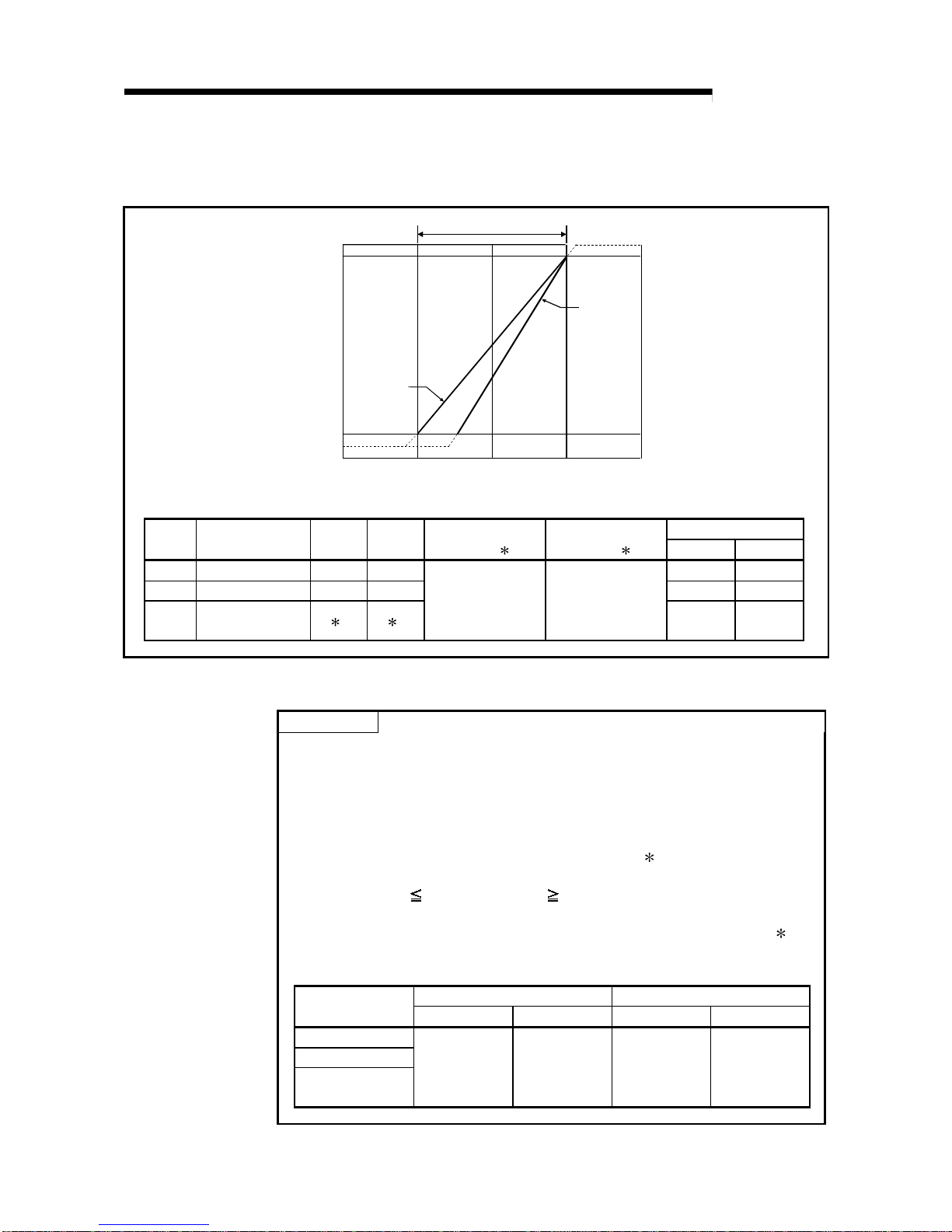
(1) Input characteristics of Q64AD-GH
(a) Voltage input characteristic
Fig. 3.1 shows a graph of the voltage input characteristic.
1)
2)
3)4)
1
65535(32767)
64000(32000)
0
-64000(-32000)
-1536(-768)
-65536(-32768)
-15 -10
-5
0
5
10 15
Digital output value
Analog input voltage (V)
Analog input practical range
The value within parentheses indicates the digital output value (16 bits).
Maximum resolution
Number
Analog input
range setting
Offset
value
Gain
value
Digital output value
(32 bits)
2
Digital output value
(16 bits) 2
32 bits 16 bits
1) 1 to 5V 1V 5V 62.5µV 125.0µV
2) 0 to 5V 0V 5V
0 to 64000 0 to 32000
78.2µV 156.4µV
3) -10 to 10V 0V 10V -64000 to 64000 -32000 to 32000
4) 0 to 10V 0V 10V
156.3µV 312.6µV
—
User range setting
(Uni-polar)
1 1
0 to 64000 0 to 32000
—
User range setting
(Bi-polar)
1 1 -64000 to 64000 -32000 to 32000
47.4µV 94.8µV
Fig. 3.1 Voltage input characteristic of Q64AD-GH
3 - 6 3 - 6
MELSEC-Q
3 SPECIFICATIONS
POINT
(1) Set within the analog input range and digital output range for each input range.
If these ranges are exceeded, the maximum resolution and accuracy may not
fall within the performance specifications. (Avoid use in the dotted area of Fig.
3.1.)
(2) Do not input an analog input voltage of more than ± 15 V. The input elements
may be damaged.
(3) Set the offset/gain values for the user setting range
1 within a range in which
the following conditions are satisfied.
(a) Offset value, gain value setting range: -10V to 10V
(b) { (gain value) - (offset value) } > 3.030V
(4) When an analog value that exceeds the range for the digital output value
2 is
entered, the digital output val ue will be fixed at the maximum or mini mum value.
Digital output value (32 bits) Digital output value (16 bits)Analog input
range setting
Minimum Maximum Minimum Maximum
1 to 5V
0 to 5V
-1536 -768
-10 to 10V -65536 -32768
0 to 10V
User range setting
(Uni-polar)
-1536 -768
User range setting
(Bi-polar)
-65536
65535
-32768
32767
3 - 7 3 - 7
MELSEC-Q
3 SPECIFICATIONS
(b) Current input characteristic
Fig. 3.2 shows a graph of the current input characteristic.
1)
2)
65535(32767)
64000(32000)
0
-1536(-768)
-10 0 10 20 30
4
Analog input practical range
Analog input voltage (mA)
Digital output value
The value within parentheses indicates the digital output value (16 bits).
Maximum resolution
Number
Analog input
range setting
Offset
value
Gain
value
Digital output value
(32 bits)
2
Digital output value
(16 bits) 2
32 bits 16 bits
1) 4 to 20mA 4mA 20mA 250.0nA 500.0nA
2) 0 to 20mA 0mA 20mA 312.5nA 625.0nA
—
User range setting
(Uni-polar)
1 1
0 to 64000 0 to 32000
151.6nA 303.2nA
Fig. 3.2 Current input characteristic of Q64AD-GH
POINT
(1) Set within the analog input range and digital output range for each input range.
If these ranges are exceeded, the maximum resolution and accuracy may not
fall within the performance specifications. (Avoid use in the dotted area of Fig.
3.2.)
(2) Do not input an analog input current of more than ± 30 mA. A breakdown may
result due to overheating.
(3) Set the offset/gain values for the user setting range
1 within a range in which
the following conditions are satisfied.
(a) Gain value
20mA, offset value 0mA
(b) { (gain value) - (offset value) } > 9.70mA
(4) When an analog value that exceeds the range of the digital output value
2 is
entered, the digital output value will be fixed at the maximum or minimum
value.
Digital output value (32 bits) Digital output value (16 bits)Analog input
range setting
Minimum Maximum Minimum Maximum
4 to 20mA
0 to 20mA
User range setting
(Uni-polar)
-1536 65535 -768 32767

3 - 8 3 - 8
MELSEC-Q
3 SPECIFICATIONS
(2) Input characteristic of Q62AD-DGH
Fig. 3.3 shows a graph of t he Q6 2AD -D GH inp ut cha ra ct eri sti c .
1)
65535(32767)
64000(32000)
0
-1536(-768)
-10 0 10 20 30
4
24
Analog input practical range
Digital output value
Analog input current (mA)
The value within parentheses indicates the digital output value (16 bits).
Maximum resolution
Number
Analog input
range setting
Offset
value
Gain
value
Digital output value
(32 bits) 2
Digital output value
(16 bits) 2
32 bits 16 bits
1) 4 to 20mA 4mA 20mA 250.0nA 500.0nA
— User range setting 1 1
0 to 64000 0 to 32000
151.6nA 303.2nA
Fig. 3.3 Input characteristic of Q62AD-DGH
POINT
(1) Set within the analog input range and digital output range for each input range.
If these ranges are exceeded, the maximum resolution and accuracy may not
fall within the performance specifications. (Avoid use in the dotted area of Fig.
3.3.)
(2) Set the offset/gain values for the user setting range
1 within a range in which
the following conditions are satisfied.
(a) Gain value
24mA, offset value 2mA
(b) { (gain value) - (offset value) } > 9.70mA
(3) When an analog value that exceeds the range of the digital output value
2 is
entered, the digital output value will be fixed at the maximum or minimum
value.
Digital output value (32 bits) Digital output value (16 bits)Analog input
range setting
Minimum Maximum Minimum Maximum
4 to 20mA
User range setting
-1536 65535 -768 32767

3 - 9 3 - 9
MELSEC-Q
3 SPECIFICATIONS
3.1.3 Accuracy
The reference accuracy is the accuracy at the ambient temperature for offset/gain
setting.
The temperature coefficient is the accuracy per temperature variation of 1°C.
The reference accuracy is the accuracy relative to the maximum value of the digital
output value.
If you change the o ffse t / ga in set ti ng or i np ut r an ge to ch ange th e in pu t ch a racte r i sti c,
the reference accuracy and temperature coefficient do not vary and kept within the
ranges given in the performance specifications.
Example) Accuracy when the temperature varies from 25°C to 30°C
0.05% (reference accuracy) + 0.00714%/°C (temperature coefficient)
5°C
(temperature variation difference) = 0.0857%

3 - 10 3 - 10
MELSEC-Q
3 SPECIFICATIONS
3.2 Function List
Table 3.3 lists the functions of the A/D converter modules.
Table 3.3 Function list
Item Function Reference section
A/D conversion
enable/disable setting
(1) Specifies whether to enable or disable the A/D conversion for each
channel.
(2) The conversion speed is 10ms regardless of the number of conv ersion
enabled channels.
Section 3.4.2
A/D conversion method
(1) Sampling processing
The A/D conversion for analog input values is performed successiv ely for
each channel, and the digital output value is output upon each conv ersion.
(2) Averaging processing
(a) Time av era ging
A/D conversion is averaged in terms of time on a channel basis and a
digital average value is output.
(b) Count averaging
A/D conversion is averaged in terms of count on a channel basis and a
digital average value is output.
(c) Move averaging
The specified number of digital output values measured per sampling time
are averaged.
(3) Primary delay filter
A digital output value is smoothed according to the preset time constant.
Section 3.2.1
Maximum and
minimum values hold
function
(1) The maximum and minimum values of the digital output v alues is reta ined
in the module.
Section 3.2.2
Input signal error
detection function
(1) The voltage/current outside the setting range is detected.
Section 3.2.3
Warning output function
(1) Process alarm
A warning is output if a digital output value falls outside the setting rang e.
(2) Rate alarm
A warning is output if the varying rate of a digital output value falls outside
the preset varying rate range.
Section 3.2.4
A/D conversion starting
time setting function
(Q62AD-DGH only)
(1) Setting the A/D conversion starting time allows A/D conversion to be
started at the point when the output of the 2-wire transmitter stabilizes. Section 3.2.5
Supply power ON/OFF
function
(Q62AD-DGH only)
(1) The power supply to the 2-wire transmitter can be switched ON/OFF
channel by channel.
(2) Power is supplied to the channel set for "Conversion enable" in the A/D
conversion enable/disable setting (buffer memory address 0: Un\G 0).
Section 3.4.2
Online module change (1) The module can be changed w ithout the sy stem being stopped. Chapter 7
3 - 11 3 - 11
MELSEC-Q
3 SPECIFICATIONS
3.2.1 A/D conversion methods
(1) Sampling processing
A/D conversion is performed successively for the analog input value, and the
converted digital output values are stored in the buffer memory.
The conversion speed is 10ms regardless of the number of conversion enabled
channels.
(2) Averaging processing
(a) Time averaging
A/D conversion is made for the preset period of time, the sum of values other
than the maximum and minimu m value s is averaged , and the result is stored
into the buffer memory .
The processing co un t wi th in t h e set ti me i s un i form independently of the
number of used channels (numbe r of chann els set for A /D conversion enable).
Processing count = set time/10 (times)
[Example] When the averaging processing time is set to 42ms
42/10 = 4.2 (times) ... Fractional portion is dropped.
(b) Count averaging
A/D conversion is made the preset number of times, the sum of values other
than the maximum and minimum values is averaged, and the result is stored
into the buffer memory.
The time when the count-based average value is stored into the buffer
memory is uniform independently of the number of used channels (number
of channels set for A/D conversion enable).
Processing time = set count
10 (ms)
[Example] When the averaging processing count is set to 5 times
5
10 = 50 (ms)
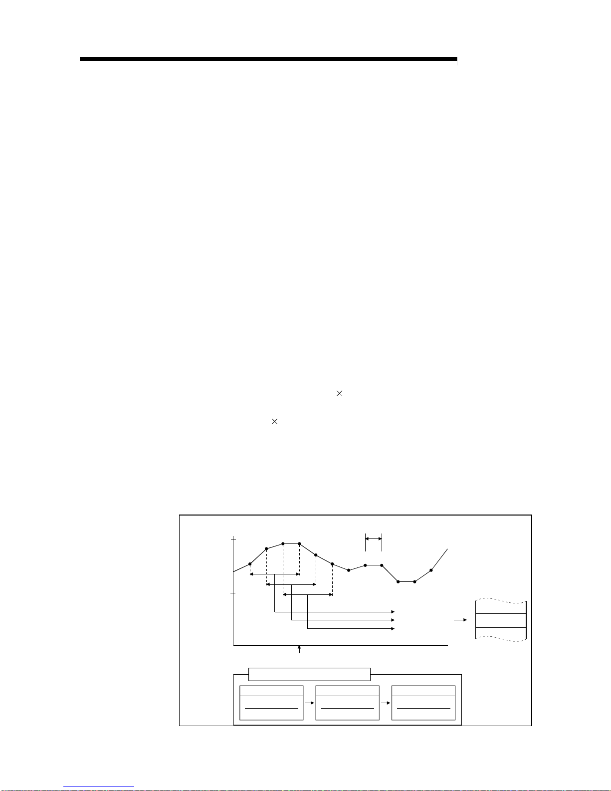
(c) Move averaging
The specified count of digital output values imported per sampling time are
averaged to find a value, which is then stored into the buffer memory.
Since average processing is performed with data shifted per sampling, the
most recent digi ta l ou tpu t va l ue is avai la bl e.
Move averaging processing at the preset count of 4 times
1)
2)
3) 4)
5)
6)
7)
8) 9)
10) 11)
12)
Time [ms]
1)+2)+3)+4)
4 4 4
Data transition inside buffer memory
64000
32000
0
Sampling time
First storage
Second storage
Third storage
Buffer memory
Digital output
value
A/D conversion completed flag ON
A
/D conversion
v
alue
First storage Second storage Third storage
2)+3)+4)+5) 3)+4)+5)+6)
3 - 12 3 - 12
MELSEC-Q
3 SPECIFICATIONS
(3) Primary delay filter
A digital value whose transient noise has been smoothed is output according to
the preset time constant.
The degree of smoothing varies with the time constant setting.
The relational expression of the time constant and digital output value is indicated
below.
[If n = 1]
Yn = 0
[If n = 2]
t
Yn = yn-
1
+
t + TA
(yn - y n -
1
)
[If n 3]
t
Yn = Yn-
1
+
t + TA
(yn - Y n -
1
)
Yn: Current digital output value yn: Pre-smoothing digital output value
Yn-
1
: Immediately preceding digital
output value
Yn-1: Immediately preceding
pre-smoothing digital output value
n: Sampling count
t: A/D conversion time (0.01s)
TA: Time constant (s)
The A/D conversion completed flag turns ON when n 2.
[Example 1] Digital output value when the analog input value varied from 0 to 1V
The variation of the digital output value at the time constant setting
of 1000ms (1s) is as shown below.
1000ms (1s) after the an alog inpu t value ha s r eache d 1 V , the digi t al
output value reaches 63.2% of the value attained when the sampling
processing is selected.
0 1000
0
0.2
0.4
0.6
0.8
1
1.2 12000
10000
0
2000
4000
6000
8000
Analog input value Digital output value
Elapsed time (ms)
Digital output value
Analog input value (V)
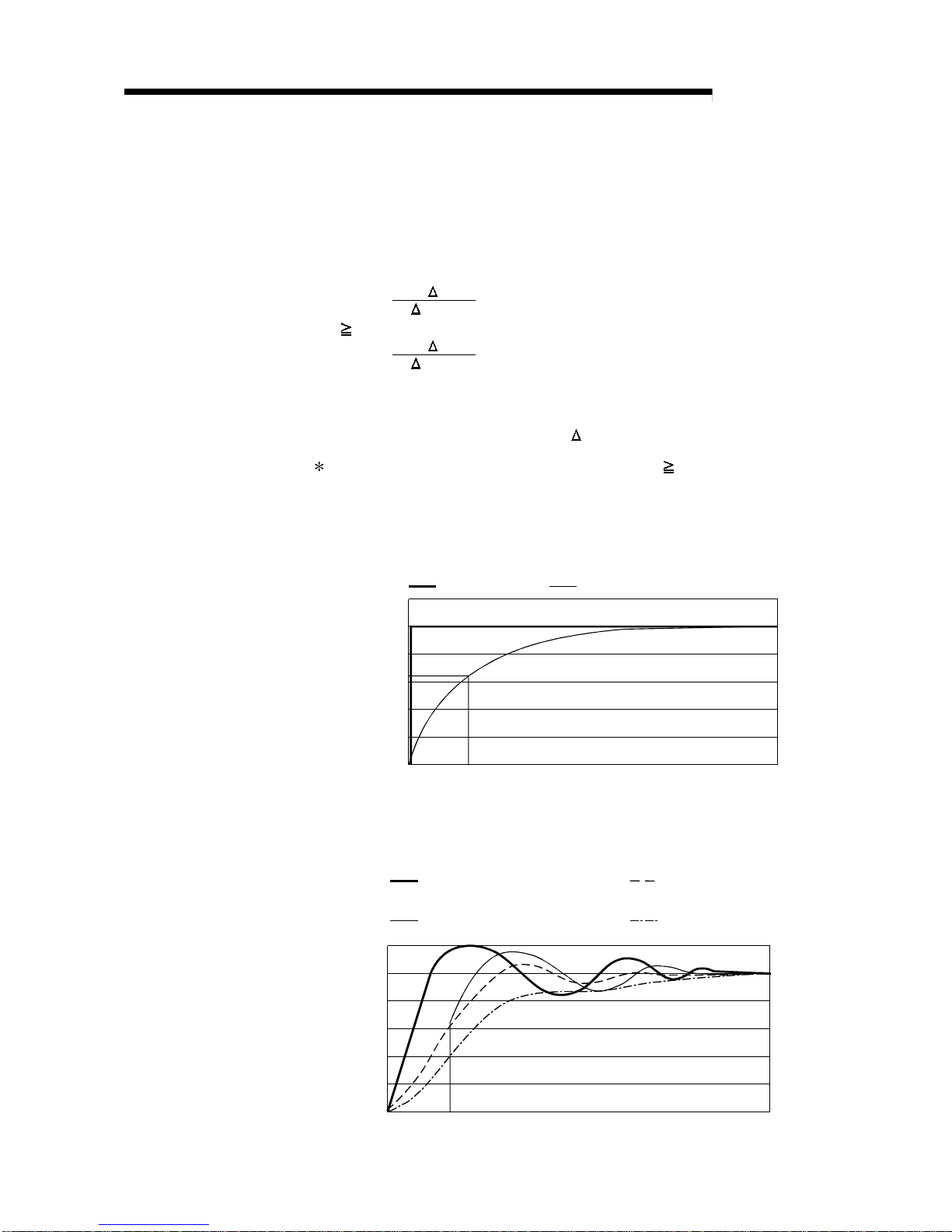
[Example 2] Digital output value when the variation of the analog input value has
a ringing waveform
The variations of the digital output values at the time constant setting
of 2000ms (2s), at the time constant setting of 1000ms (1s), and at
the move averaging processing of 16 times are as shown below.
0
0
0.2
0.4
0.6
0.8
1
1.2
12000
10000
0
2000
4000
6000
8000
Analog input value (V)
Digital output value
(time constant setting: 1000ms)
Analog input value
Digital output value
(move averaging processing: 16 times)
Digital output value
(time constant setting: 2000ms)
Elapsed time (ms)
Digital output value

3 - 13 3 - 13
MELSEC-Q
3 SPECIFICATIONS
3.2.2 Maximum and minimum v al ues hol d function
(1) The maximum and minimum values are held in the buffer memory channel by
channel.
(2) The maximum and minimum values are cleared to 0 when the maximum
value/minimum value reset request (YD) or operating condition setting request
(Y9) is turned ON, and new maximum and minimum values are stored when
conversion is started.
(3) Since the area for storing the maximum and minimum values can be rewritten with
the sequence program, the maximum and minimum values within a specific period
of time can be checked.
3.2.3 Input signal error detection function
(1) If the input voltage/current rose to or above the input signal error detection upper
limit value or fell to or below the lower limit value, the input signal error detection
flag (buffer memory address 49: Un\G49) and input signal error detection signal
(XC) turn ON and the ALM LED flickers to indicate the error.
(2) The digital ou tput v alue of t he chan ne l w he re th e inpu t sign al er ro r det e ctio n fl ag
(buffer memory address 49: Un\G49) turned ON is held as immediately before
detection of the error, and the A/D conversion completed flag (buffer memory
address 10: Un\G 10) of the co rres p ondin g ch an nel tu rn s OF F.
(3) By bringing the analog input value within the setting range and then turning ON
the error clear request (YF), the input signal error detection flag (buffer memory
address 49: Un\G49) and input signal error detection signal (XC) turn OFF.
(4) When the analog input value returns to within the setting range, A/D conversion is
resumed independently of whether the input signal error detection flag (buffer
memory address 49: Un\G49) and input signal error detection signal (XC) are
reset or not, the A/D conversion completed flag (buffer memory address 10:
Un\G10) of the corresponding channel turns ON again after the first updating.
(The ERR. LED remains flickering.)
Analog input value
Error detecti o n
Upper limit
value
CH1 analog
input value
Lower limit
value
Input value
normal
Time
CH1 input signal error detection flag
(Buffer memory address 49, b0)
Input signal error detection signal (XC)
CH1 A/D conversion completed flag
(Buffer memory address 10, b0)
Error clear request (YF)
3 - 14 3 - 14
MELSEC-Q
3 SPECIFICATIONS
(5) This function is executed at every sampling processing.
(6) Perform the following procedure to use this function.
1) Set the input signal error detection setting value for th e correspon ding channe l.
2) Enable the A/D conve rsion of the corresponding channel.
3) Enable the input signal error detection of the corresponding channel.
4) Turn ON the operating condition setting request (Y9).
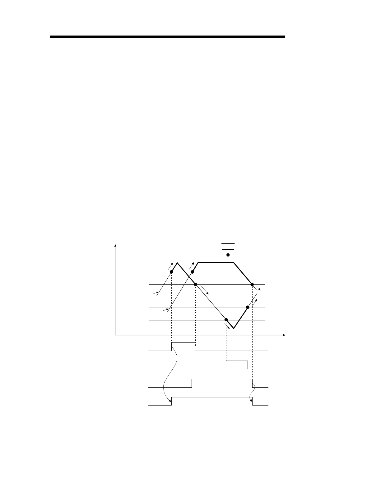
3.2.4 Warning output function
(1) Process alarm
(a) If the detected digital output value rose to or above the process alarm upper
upper limit value or fell to or below the process alarm lower lower limit value
and entered the warning output range zone, the warning output flag (buffer
memory address 48: Un\G48) and warning output signal (X8) turn ON and
the ALM LED is lit to indicate the warning.
(b) If, after the output of the warning, the detected digital output value fell below
the process alarm upper lower limit value or rose above the process alarm
lower upper limit value and returned to within the setting range, "0" is stored
into the bit position corresponding to the channel number of the warning
output flag (buffer memory address 48: Un\G48).
The warning outp u t signal ( X8 ) t u rns OF F only wh en all chan nel s r etu r n to
within the setting range.
Digital output value
Upper upper
limit value
Upper lower
limit value
CH1 digital output
value
Lower upper
limit value
CH2 digital
output value
Lower lower
limit value
Warning
occurrence
Warning
occurrence
Warning output range zone
Warning output range outside zone
Included
Warning cancel
Warning
occurrence
Warning cancel
Warning cancel
CH1 process alarm upper limit value
(Buffer memory address 48, b0)
CH1 process alarm lower limit value
(Buffer memory address 48, b1)
CH2 process alarm upper limit value
(Buffer memory address 48, b2)
Time
Warning output signal (X8)
(c) When time or count averaging is specified, this function is executed at
intervals of the preset averaging time or averaging count.
When any other A/D conversion system (sampling processing, move
averaging, primary delay filter) is specified, this function is executed at
intervals of the sampling time.
3 - 15 3 - 15
MELSEC-Q
3 SPECIFICATIONS
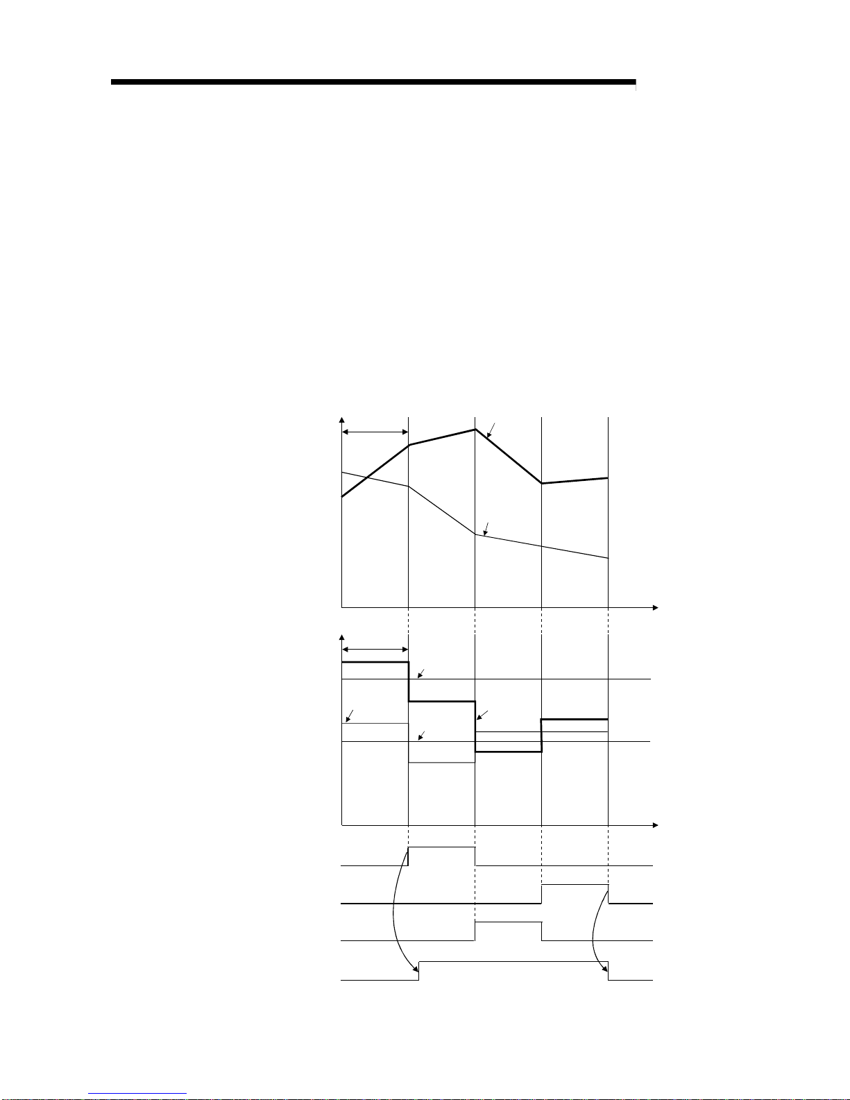
(2) Rate alarm
(a) If the digital output value sampled at intervals of the rate alarm warning
detection period indicated a varying rate equal to or greater than the rate
alarm upper limit value or a varying rate equal to or less than the rate alarm
lower limit value, the warning output flag (buffer memory address 48:
Un\G48) and warning output signal (X8) turn ON and the ALM LED is lit to
indicate the warning of the rate alarm.
(b) If, after the output of the warning, the varying rate fell below the rate alarm
upper limit value or rose above the rate alarm lower limit value and returned
to within the setting range, "0" is stored into the bit position corresponding to
the channel number of the warning output flag (buffer memory address 48:
Un\G48).
The warning outp u t signal ( X8 ) t u rns OF F only wh en all chan nel s r etu r n to
within the setting range.
Digital output value
Rate alarm
warning detection
period
CH1 digital
output value
CH2 digital
output value
Time
Varying rate (%) of
digital output value
Rate alarm
warning detection
period
Rate alarm
upper limi t
value
Varying rate of
CH2 digital
output value
Rate alarm
lower limit
value
Varying rate of
CH1 digital
output value
Time
CH1 rate alarm upper limit value
(Buffer memory address 48, b8)
CH1 rate alarm lower lim it va lue
(Buffer memory address 48, b9)
CH2 rate alarm lower lim it va lue
(Buffer memory address 48, b11)
Warning output signal (X8)

3 - 16 3 - 16
MELSEC-Q
3 SPECIFICATIONS
(c) Set the rate alarm upper limit value/lower limit value in 0.1%/s increments
relative to the maxi mu m val u e (640 00 ) o f th e di gi tal output value.
The setting range is -65536 to 65535 (-6553.6% to 6553.5%).
(d) The setting range of the rate alarm warning detection period is 10 to
5000ms.
When the period is set to 5000ms, the digital values are compared at
intervals of 5 seconds to det ect t he vary ing rate.
(e) The rate alarm is judged by converting the rate alarm upper/lower limit value
into the digit value per rate alarm warning detection period.
The conversion expression of the value used to make judgment per rate
alarm warning detection period is as follows.
Value used to make judgment per rate alarm warning detection period [digit]
=rate alarm upper limit value or lower limit value
0.001 64000 rate
alarm warning detection period ÷ 1000
Example
When the varying rate upper limit value of channel 1 is set to 30%/s (300 is
stored into the bu ffe r me mory) and the rate alarm warning dete cti o n per io d o f
channel 1 is 10ms, the current and previous values are compared at intervals of
10ms and whether or not the value has varied 0.3% (192 digits) or more in 10ms
is judged.
300
0.001 64000 10÷1000 =192(digit)
(f) The rate alarm is useful to watch the varying rate of the digital output value in
the limited range.
1) Example of setting the rate alarm upper limit value/lower limit value
when it is desired to watch that the digital output value is at the rise rate
within the specified range
+30%
+20%
0
Varying rate (%) of
digital output value
Rate alarm upper limit value
Rate alarm lower limit va lue
Time

3 - 17 3 - 17
MELSEC-Q
3 SPECIFICATIONS
2) Example of setting the rate alarm upper limit value/lower limit value
when it is desired to watch that the digital output value is at the fall rate
within the specified range
-30%
-20%
0
V
arying rate (%) of
digital output value
Rate alarm upper limit value
Rate alarm lower limit valu e
Time
3) Example of setting the rate alarm upper limit value/lower limit value
when it is desired to watch that the digital output value is at the varying
rate within the specified range
-10%
+10%
0
V
arying rate (%) of
digital output value
Rate alarm upper limit value
Rate alarm lower limit value
Time

3 - 18 3 - 18
MELSEC-Q
3 SPECIFICATIONS
3.2.5 A/D conversion starting time setting function ( Q62AD- D GH only)
(1) As the A/D conversion starting time, set the "time necessary from when the used
2-wire transmitter powers on u ntil its output stabilizes".
This setting allows A/D conversion processing to be started as soon as the output
of the 2-wire transmitter stabiliz e s.
(2) Set the time to the CH
A/D conversion starting time setting (buffer memory
addresses 5, 6: Un\G5, Un\G6).
(3) The following indicates the time until the A/D conversion completed flag (buffer
memory addresses 10: Un\G10) turns ON when the A/D conversion starting time
has been set.
(A/D conversion starting time) + (A/D conversion pre-processing: Approx. 150 to
165ms) + (A/D conversion processing: 10ms)
POINT
Set the A/D conversion starting time in consideration of the time necessary from
when the 2-wire tran smit te r pow er s on until it s outpu t sta biliz es an d the warm-up
time of the 2-wire transmitter.
ON
ON
[Example] When the time necessary from when the 2-wire transmitter powers on until its output stabilizes is 500ms
A/D conversion enable/disable setting
(Power supply to 2-wire transmitter
ON/OFF)
(Buffer memory address 0: Un\G0)
26V power supply to 2-wire transmitter
Analog output of 2-wire transmitter
A/D conversion completed flag when A/D
conversion starting time is set to 500ms
(Buffer memory address 10: Un\G10)
A/D conversion completed flag when A/D
conversion starting time is set to 0ms
(Buffer memory address 10: Un\G10)
A/D conversion enable
Power ON
Max.
20ms
When A/D conversion starting time is 0ms,
A/D conversion processing starts at this point.
When A/D conversion starting time is 500ms,
A/D conversion processing starts at this point.
500ms
(A/D conversion
starting time)
10ms
(A/D conversion
processing time)
Approx.150 to 165ms
(A/D conversion
pre-processing)
Approx.
150 to 165ms
(A/D conversion
pre-processing)
10ms (A/D conversion processing time)

3 - 19 3 - 19
MELSEC-Q
3 SPECIFICATIONS
3.3 I/O Signals for the PLC CPU
3.3.1 List of I/O signals
Table 3.4 lists the I/O signals of the Q64AD-GH.
Table 3.5 lists the I/O signals of the Q62AD-DGH.
Note that I/O numbers (X/Y) shown in this chapter and thereafter are the values when
the start I/O number for the A/D converter module is set to 0.
Table 3.4 List of I/O signal (Q64AD-GH)
Signal direction CPU Module Q64AD-GH Signal direction CPU Module Q64AD-GH
Dev ic e N o . ( In p ut ) Signal name Dev ic e N o . ( Ou t pu t ) Signal name
X0 M odule ready Y0
X1 Y1
X2 Y2
X3 Y3
X4 Y4
X5 Y5
X6 Y6
X7
Use prohibited
1
Y7
X8 Warning output s ignal Y8
Use prohibited
1
X9 Oper a t in g c on d it i on se t ti ng c om pl e t ed fl ag Y9 Operating condition setting request
XA Offset/gain setting mode flag YA User range writing request
XB Channel change completed flag YB Channel change request
XC Input signal error detection signal YC
Use prohibited
1
XD
Maximum value/minimum value reset
completed flag
YD
Maximum value/minimum value reset
request
XE A/D conversion completed flag YE
Use prohibited
1
XF Error flag YF Error clear request
POINT
1 These signals cannot be used by the user since they are for system use only.
If these are turned ON/OFF by the sequence program, the functioning of the
A/D converter module cannot be guaranteed.

3 - 20 3 - 20
MELSEC-Q
3 SPECIFICATIONS
Table 3.5 List of I/O signal (Q62AD-DGH)
Signal direction CPU Module Q62AD-DGH Signal direction CPU Module Q62AD-DGH
Dev ic e N o . ( In p ut ) Signal name Dev ic e N o . ( Ou t pu t ) Signal name
X0 Module ready Y0
X1 Y1
X2 Y2
X3 Y3
X4 Y4
X5 Y5
X6 Y6
X7
Use prohibited
1
Y7
X8 Warning output signal Y8
Use prohibited
1
X9 Oper a t in g c on d it i on se t ti ng c om pl e t ed fl ag Y9 Operating condition setting request
XA Offset/gain setting mode flag YA User range writing request
XB Channel change completed flag YB Channel change request
Input signal error detection signal
XC
Offset/gain change completed flag
YC Offset/gain change request
XD
Maximum value/minimum value reset
completed flag
YD
Maximum value/minimum value reset
request
XE A/D conversion completed flag YE
Use prohibited
1
XF Error flag YF Error clear request
POINT
1 These signals cannot be used by the user since they are for system use only.
If these are turned ON/OFF by the sequence program, the functioning of the
A/D converter module cannot be guaranteed.
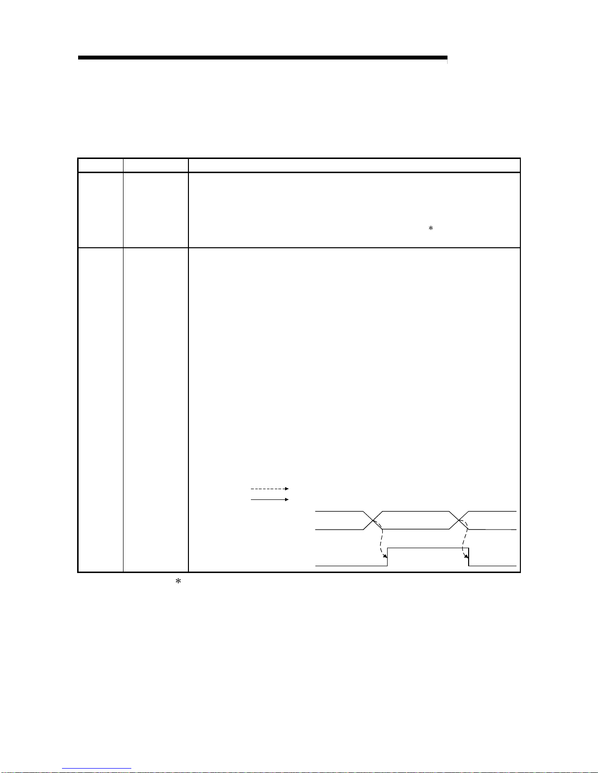
3 - 21 3 - 21
MELSEC-Q
3 SPECIFICATIONS
3.3.2 Details of I/O signals
I/O signals for the A/D converter modules are explained in detail below.
(1) Input signals
Device No. Signal Name Description
X0 Module ready
(1) When the PLC CPU is powered on or reset, this signal turns on once the preparation for
A/D conversion has been completed, and A/D conversion proces sin g is then performed.
(2) In either of the following states, the Module ready (X0) turns OFF.
• During offset/gain setting mode (A/D conversion processing is p erformed.)
• When the A/D converter module has a watchdog timer error
1
(A/D conversion
processing is not performed.)
X8
Warning output
signal
(1) The Warning output signal (X8) turns ON at detection of a process alarm or rate alarm.
(a) Process alarm
1) This signal turns ON when the digital output value falls outside th e setting ra nge
set to the process alarm upper/lower limit values (buffer memory addresse s 86
to 117: Un\G86 to Un\G117) on any of the channels enabled for A/D conversion
after the process alarm function has been made valid.
2) As soon as the digital output values return to within the setting ranges on all
channels enabled for A/D conversion, this signal turns OFF automatica lly and
the ALM LED is also extinguished.
(b) Rate alarm
1) This signal turns ON when the varying rate of the digital output value fal ls
outside the varying rate range set to the rate alarm upper/lower limit values
(buffer memory addresses 122 to 137: Un\G122 to Un\G137) on any of the
channels enabled for A/D conversion after the rate alarm function has been
made valid.
2) As soon as the varying rates of the digital output values return to within the
preset varying ranges on all channels enabled for A/D conversion, this si gnal
turns OFF automatically and the ALM LED is also extinguished.
00
Performed by the A/D converter module
Performed by the sequence program
Warning output flag
(Buffer memory address 48: Un\G48)
Warning occurrence
(Process alarm, rate alarm)
Warning output signal (X8
)
1 A watchdog timer error occurs when the program calculations are not c omplete d w ithin the
scheduled time due to malfunctions of A/D converter module hardw are.
When a watchdog timer error occurs, the RUN LED for the A/D converter module turns off.
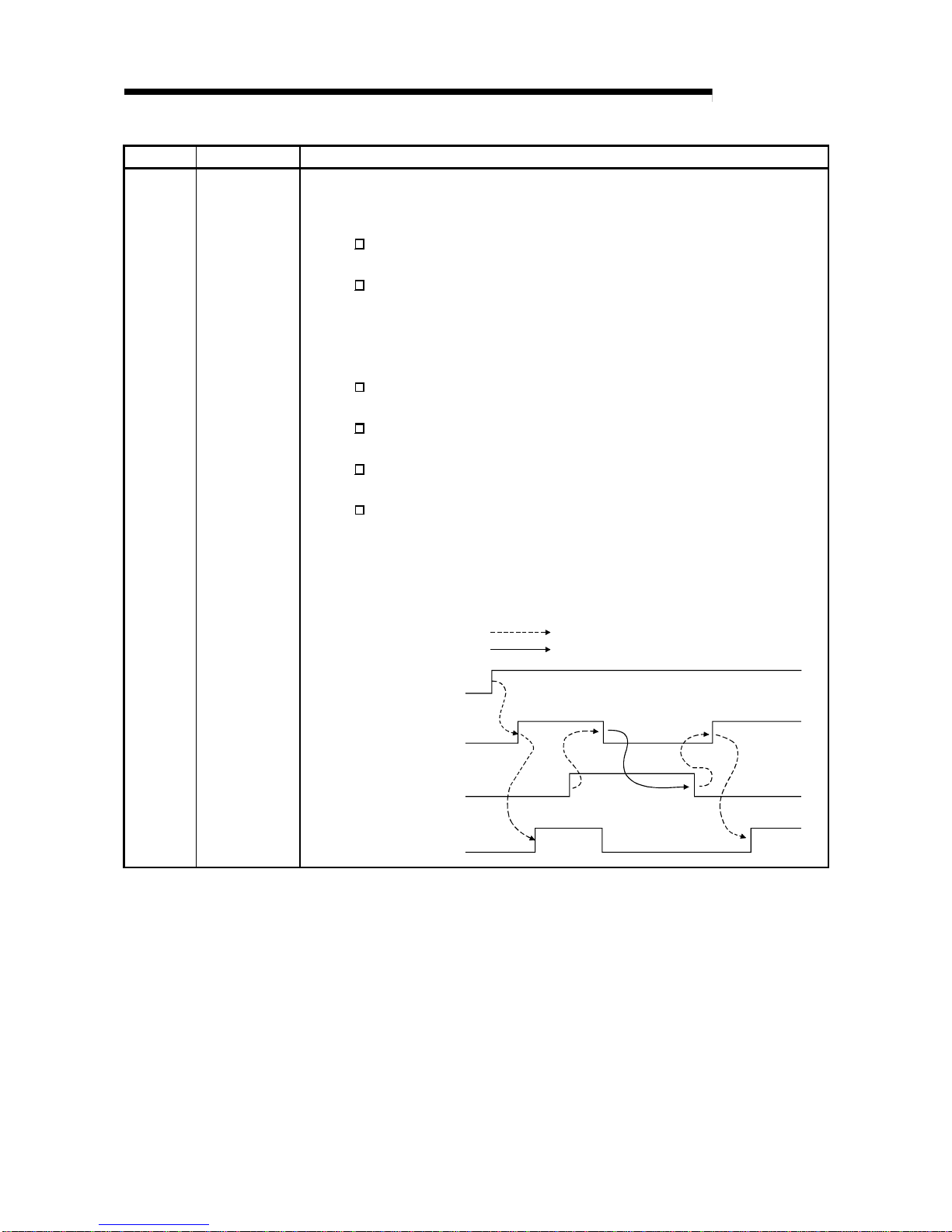
3 - 22 3 - 22
MELSEC-Q
3 SPECIFICATIONS
Device No. Signal Name Description
X9
Operating
condition setting
completed flag
(1) This signal is used as an interlock condition to turn ON/O FF the O perating condition
setting request (Y9) when any of the following settings has been changed.
• A/D conversion enable/disable setting (buffer memory address 0: Un\G 0)
• CH
Average time/Average number of times/Move average/Time constant settings
(buffer memory addresses 1 to 4: Un\G1 to Un\G4)
• CH A/D conversion starting time setting (buffer memory addresses 5, 6: Un\G 5,
Un\G6)
• Averaging process specification (buffer memory address 9: Un\G9)
• Input signal error detection/warning output settings (buffer memory address 47:
Un\G47)
• CH
process alarm upper/lower limit value (buffer memory addresses 8 6 to 117:
Un\G86 to Un\G117)
• CH
rate alarm warning detection period (buffer memory addresses 118 to 121:
Un\G118 to Un\G121)
• CH rate alarm upper/lower limit value (buffer memory addresses 122 to 137:
Un\G122 to Un\G137)
• CH
input signal error detection setting value (buffer memory addresses 138 to 141:
Un\G138 to Un\G141)
(2) When the operating condition setting completed flag (X9) is OFF, A/D conv ersion
processing is not performed. Under the following conditions, the operating condition
setting completed flag (X9) turns OFF.
• When operating condition setting request (Y9) is ON
Performed by the A/D converter module
Performed by the sequence program
A/D conversion
completed flag (XE)
Module ready (X0)
Operating condition
setting completed flag (X9)
Operating condition
change request (Y9)

3 - 23 3 - 23
MELSEC-Q
3 SPECIFICATIONS
Device No. Signal Name Description
[In offset/gain setting mode]
(1) This signal is used as an interlock condition to turn ON/O FF the User range writing
request (YA) when the value at completion of offset/gain setting adju stment i s
registered.
(2) See Section 4.6 regarding the offset/gain settings.
OFF
Module ready (X0)
Offset/gain setting mode flag (XA)
User range writing request (YA)
Performed by the A/D converter module
Performed by the sequence program
XA
Offset/gain
setting mode flag
[In normal mode]
(1) This signal is used as an interlock condition to turn ON/O FF the User range writing
request (YA) when the user range is restored.
(2) Refer to Chapter 7 for the user range restoration.
ON
Performed by the A/D converter module
Performed by the sequence program
Module ready (X0)
Offset/gain setting mode flag (XA)
User range writing request (YA)

3 - 24 3 - 24
MELSEC-Q
3 SPECIFICATIONS
Device No. Signal Name Description
XB
Channel change
completed flag
(1) This is used as an interlock condition for setting the channel cha nge reque st (YB) to
ON/OFF when changing the channel for which the offset/gain sett ings are to b e
performed.
(2) See Section 4.6 regarding the offset/gain settings.
Channel change request (YB)
Offset/gain setting mode
Offset/gain specifications
(buffer memory addresses 22, 23:
Un\G22, Un\G23)
Channel change completed
flag (XB)
Performed by the A/D converter module
Performed by the sequence program
XC
Input signal error
detection signal
(1) This signal turns ON when the analog input value falls outside the setting rang e set to
the Input signal error detection setting value (buffer memory addresses 138 to 1 41:
Un\G138 to Un\G141) on any of the channels enabled for A/D conversion after the Input
signal error detection is made valid.
(2) When the Input signal error detection signal turns ON
1) The A/D conversion completed flag (buffer memory address 10: Un\G10) of the
corresponding channel turns OFF.
2) The digital output value is held as at the time of error detection.
3) The ALM LED flickers.
(3) By bringing the analog input value within the setting range and then turning ON the Error
clear request (YF), the Input signal error detection signal (XC) turns OFF and the ALM
LED is extinguished.
(4) When the analog input value returns to within the setting range, A/D conversion is
resumed independently of whether the Input signal error detection signal (X C ) is reset or
not, and after the first updating, the A/D conversion completed flag (buffer memory
address 10: Un\G10) of the corresponding channel turns ON again.
The processing, such as averaging processing or primary delay filter, starts from the first
time after resumption of A/D conversion.
0 0
Performed by the A/D converter module
Performed by the sequence program
Input signal error detection flag
(Buffer memory address 49:
Un\G49)
Input signal error detection signal
(XC)
Error clear request (YF)
Input signal error
detection

3 - 25 3 - 25
MELSEC-Q
3 SPECIFICATIONS
Device No. Signal Name Description
XC
Offset/gain
change
completed flag
1
(1) This signal is used as an interlock condition to turn ON/O FF the offset/gain ch ange
request (YC) when the offset/gain value is changed.
(2) Refer to Section 4.6 for the offset/gain setting.
Performed by the A/D converter module
Performed by the sequence program
Offset/gain change completed flag
(XC)
Offset/gain change request (YC)
XD
Maximum
value/minimum
value reset
completed flag
(1) This signal turns ON when the maximum value/minimu m v alue stored at any of the
buffer memory addresses 30 to 37, 62 to 77 (Un\G30 to Un\G37, Un\G62 to Un\G 77) is
reset when the Maximum value/minimum value reset request (YD) turns ON.
Maximum value/minimum value
reset completed flag (XD)
Maximum and minimu m values
storage area
Buffer memory addresses 30 to 37,
62 to 77 (Un\G30 to Un\G37,
Un\G62 to Un\G77)
Maximum value/minimum value
reset request (YD)
Performed by the A/D converter module
Performed by the sequence program
XE
A/D conversion
completed flag
(1) This turns ON when conversion for all of the channels that are conversion enabl ed has
been completed.
(2)
1
When the external supply power to the Q62AD-DGH switches OFF, the A/D
conversion completed flag turns OFF, the digital output values are he ld as prev iously ,
and A/D conversions stop.
When the external supply power switches ON, A/D conversions resume, and a s soo n as
all conversion-enabled channels have completed conv ersions, th e A/D conv ersion
completed flag turns ON.
The processing, such as averaging processing or primary delay filter, starts from the first
time after resumption of A/D conversion.
XF Error flag
(1) The error flag turns ON when a write error occurs.
(2) To clear the error code, set the error clear request (YF) to ON.
The error code is read during this interval.
Error flag (XF)
Error clear request (YF)
Performed by the A/D converter module
Performed by the sequence program
1: Q62AD-DGH only
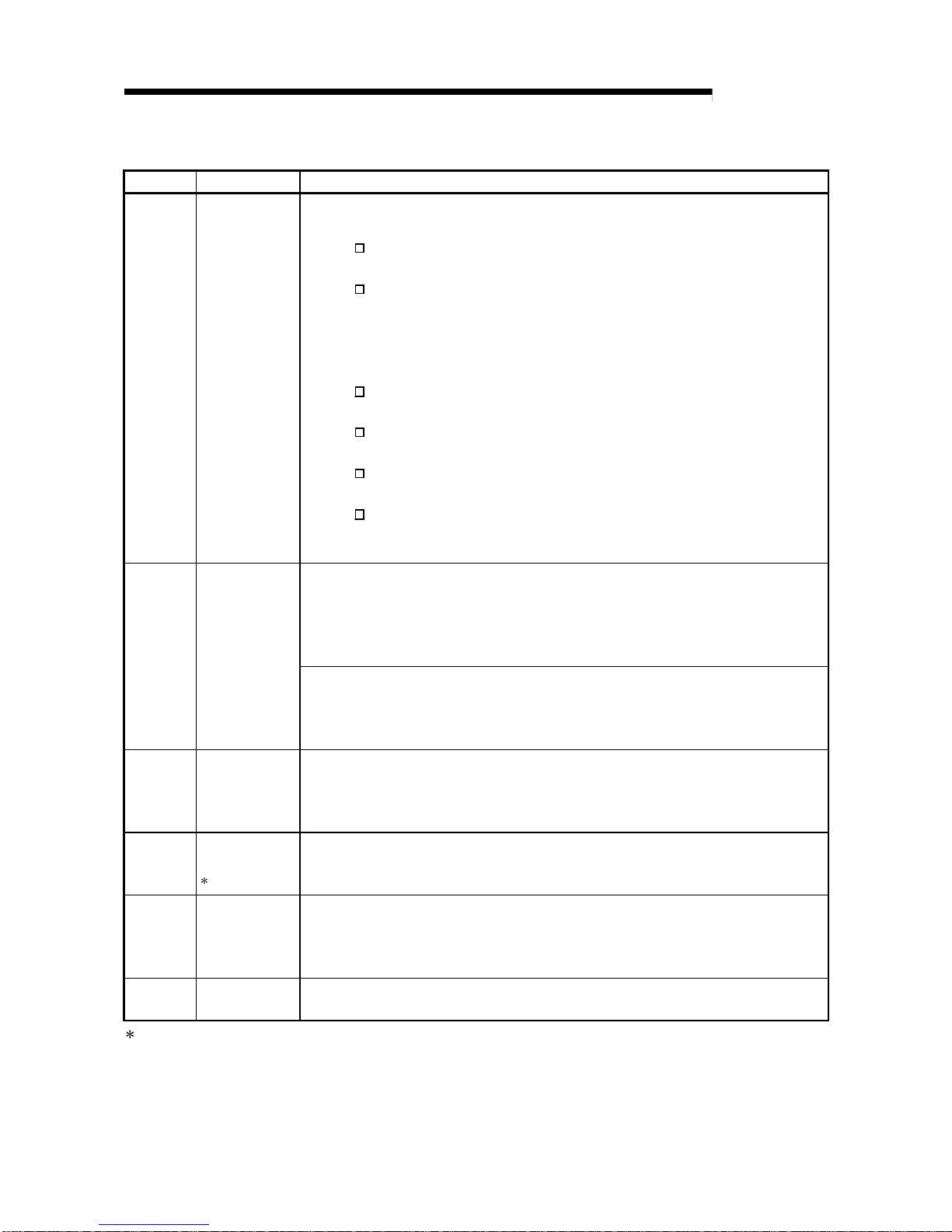
3 - 26 3 - 26
MELSEC-Q
3 SPECIFICATIONS
(2) Output signals
Device No. Signal Name Description
Y9
Operating
condition setting
request
(1) Turn this signal ON when making any of the following settings v alid.
• A/D conversion enable/disable setting (buffer memory address 0: Un\G 0)
• CH
Average time/Average number of times/Move average/Time constant settings
(buffer memory addresses 1 to 4: Un\G1 to Un\G4)
• CH A/D conversion starting time setting (buffer memory addresses 5, 6: Un\G 5,
Un\G6)
• Averaging process specification (buffer memory address 9: Un\G9)
• Input signal error detection/warning output settings (buffer memory address 47:
Un\G47)
• CH
process alarm upper/lower limit value (buffer memory addresses 8 6 to 117:
Un\G86 to Un\G117)
• CH
rate alarm warning detection period (buffer memory addresses 118 to 121:
Un\G118 to Un\G121)
• CH rate alarm upper/lower limit value (buffer memory addresses 122 to 137:
Un\G122 to Un\G137)
• CH
input signal error detection setting value (buffer memory addresses 138 to 141:
Un\G138 to Un\G141)
(2) See the X9 column for ON/OFF timing.
[In offset/gain setting mode]
(1) This turns ON when the value for the adjusted offset/gain settings are registere d in the
A/D converter module.
(2) See the XA column for ON/OFF timing.
See Section 4.6 for offset/gain settings.
YA
User range
writing request
[In normal mode]
(1) This signal turns ON when the user range is restored.
(2) Refer to the field of XA for the ON/OFF timing.
Refer to Chapter 7 for user range restoration.
YB
Channel change
request
(1) This turns ON when changing the channel for which offset/gain sett ings are to be
performed.
(2) See the XB column for ON/OFF timing.
See Section 4.6 for offset/gain settings.
YC
Offset/gain
change request
1
(1) Turn this signal ON when changing the offset/gain value.
(2) Refer to the field of XC for the ON/OFF timing.
Refer to Section 4.6 for the offset/gain setting.
YD
Maximum
value/minimum
value reset
request
(1) Turning ON the Maximum value/minimum value reset request (Y D ) clears the maximum
value/minimum value stored at any of the buffer memory addresses 30 to 37, 62 to 77
(Un\G30 to Un\G37, Un\G62 to Un\G77).
(2) See the XD column for ON/OFF timing.
YF
Error clear
request
(1) Turn this signal ON when clearing a write error or input signal error.
(2) Refer to the field of XF or XC for the ON/OFF timing.
1: Q62AD-DGH only

3 - 27 3 - 27
MELSEC-Q
3 SPECIFICATIONS
POINT
When the User range writing request (YA) is turned ON in the normal mode with
A/D conversion enabled, the A/D converter module restores the user range.
Offset/gain setting mode flag (XA)
User range writing request (YA)
User range restoration processing
A/D conversion completed flag
(Buffer memory address 10: Un\G10)
Digital output value
(Buffer memory addresses 11 to 14,
54 to 61: Un\G11 to 14, Un\G54 to 61)
Power of 2-wire transmitter
During restoration
Restoration
completed
Power ON
Power OFF
Power ON
During user range restoration: A/D conversion stop, A/D conversion completed flag
(buffer memory addresses 10: Un\G10) OFF, digital
output value held as previously, power of 2-wire
transmitter OFF (Q62AD-DGH only)
After user range restoration: A/D conversion resumed (when user range setting is
used, A/D conversion is resumed at the restored
offset/gain se tt in g val ue . )
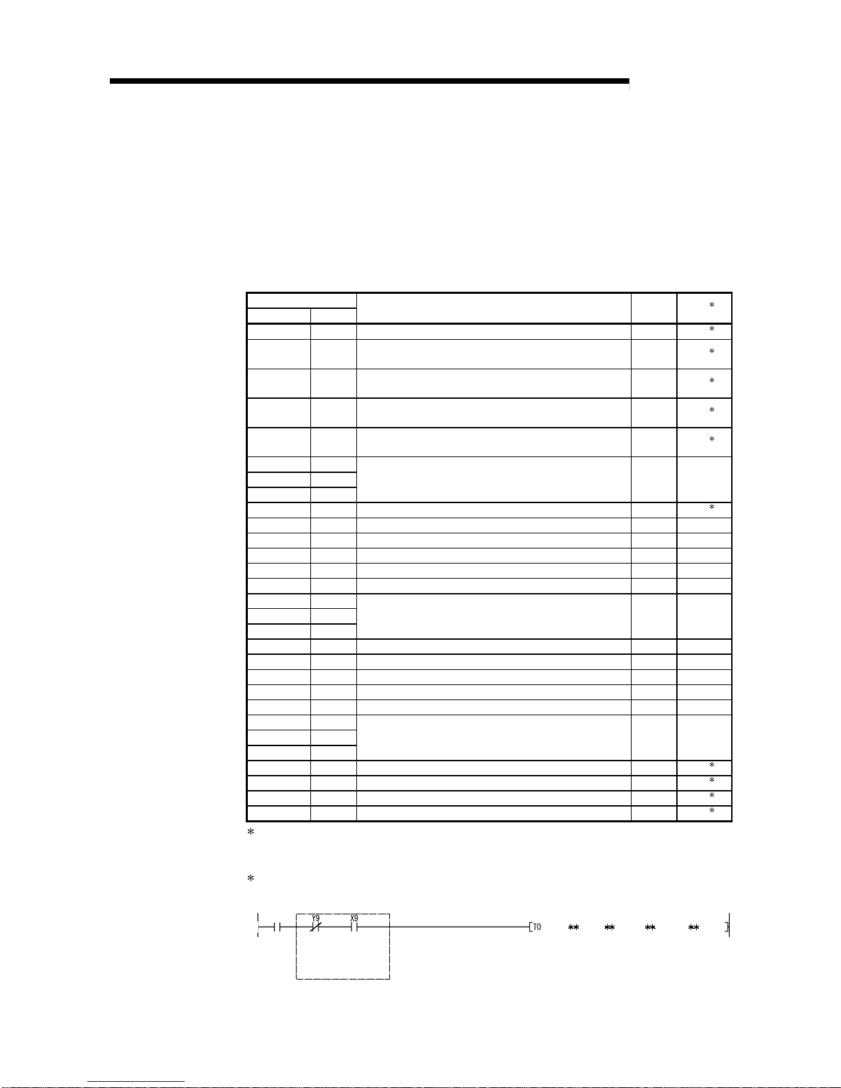
3 - 28 3 - 28
MELSEC-Q
3 SPECIFICATIONS
3.4 Buffer Memory
3.4.1 Buffer memory assignment
This section describes the buffer memory assignments of the A/D converter modules.
(1) Buffer memory assignment of Q64AD-GH
Table 3.6 Buffer memory assignment o f Q64AD -GH ( 1/5)
Address
Hexadecimal Decimal
Description Default R/W
1
0
H
0 A/D conversion enable/disable setting 0000HR/W
2
1
H
1
CH1 Average time/Average number of times/Move average
/Time constant settings
0R/W
2
2
H
2
CH2 Average time/Average number of times/Move average/
Time constant settings
0R/W
2
3
H
3
CH3 Average time/Average number of times/Move average/
Time constant settings
0R/W
2
4
H
4
CH4 Average time/Average number of times/Move average/
Time constant settings
0R/W
2
5
H
5
to to
8
H
8
System area — —
9
H
9 Averaging process specification 0 R/W
2
A
H
10 A/D conversion completed flag 0 R
B
H
11 CH1 Digital output value(16Bit) 0 R
C
H
12 CH2 Digital output value(16Bit) 0 R
D
H
13 CH3 Digital output value(16Bit) 0 R
E
H
14 CH4 Digital output value(16Bit) 0 R
F
H
15
to to
12
H
18
System area — —
13
H
19 Error code 0 R
14
H
20 Setting range 0 R
15
H
21 System area — —
16
H
22 Offset/gain setting mode offset specification 0 R/W
17
H
23 Offset/gain setting mode gain specification 0 R/W
18
H
24
to to
1D
H
29
System area — —
1E
H
30 CH1 Maximum value(16Bit) 0 R/W
2
1F
H
31 CH1 Minimum value(16Bit) 0 R/W
2
20
H
32 CH2 Maximum value(16Bit) 0 R/W
2
21
H
33 CH2 Minimum value(16Bit) 0 R/W
2
1 Indicates whether reading and writing to/from a sequence program are enabled.
R : Read enabled
W : Write enabled
2 When writing data to the buffer memory, always perform write under the interlock conditions (buffer
memory write conditions) of the following I/O signals.
Writing
request
Buffer memory writing conditions
Operating
condition
setting
request
Operating
condition
setting
completed
flag

3 - 29 3 - 29
MELSEC-Q
3 SPECIFICATIONS
Table 3.6 Buffer memory assignment o f Q64AD -GH ( 2/5)
Address
Hexadecimal Decimal
Description Default R/W
1
22
H
34 CH3 Maximum value(16Bit) 0 R/W
2
23
H
35 CH3 Minimum value(16Bit) 0 R/W
2
24
H
36 CH4 Maximum value(16Bit) 0 R/W
2
25
H
37 CH4 Minimum value(16Bit) 0 R/W
2
26
H
38
to to
2E
H
46
System area — —
2F
H
47 Input signal error detection/warning output settings 0FFFHR/W
2
30
H
48 Warning output flag 0 R
31
H
49 Input signal error detection flag 0 R
32
H
50
to to
35
H
53
System area — —
36
H
54
37
H
55
CH1 Digital output value(32Bit) (L)
(H)
0R
38
H
56
39
H
57
CH2 Digital output value(32Bit) (L)
(H)
0R
3A
H
58
3B
H
59
CH3 Digital output value(32Bit) (L)
(H)
0R
3C
H
60
3D
H
61
CH4 Digital output value(32Bit) (L)
(H)
0R
3E
H
62
3F
H
63
CH1 Maximum value(32Bit) (L)
(H)
0R/W
2
40
H
64
41
H
65
CH1 Minimum value(32Bit) (L)
(H)
0R/W
2
42
H
66
43
H
67
CH2 Maximum value(32Bit) (L)
(H)
0R/W
2
44
H
68
45
H
69
CH2 Minimum value(32Bit) (L)
(H)
0R/W
2
46
H
70
47
H
71
CH3 Maximum value(32Bit) (L)
(H)
0R/W
2
48
H
72
49
H
73
CH3 Minimum value(32Bit) (L)
(H)
0R/W
2
4A
H
74
4B
H
75
CH4 Maximum value(32Bit) (L)
(H)
0R/W
2
4C
H
76
4D
H
77
CH4 Minimum value(32Bit) (L)
(H)
0R/W
2
4E
H
78
to to
55
H
85
System area — —
1 Indicates whether reading and writing to/from a sequence program are enabled.
R : Read enabled
W : Write enabled
2 When writing data to the buffer memory, always perform write under the interlock conditions (buffer
memory write conditions) of the following I/O signals.
Writing
request
Buffer memory writing conditions
Operating
condition
setting
request
Operating
condition
setting
completed
flag
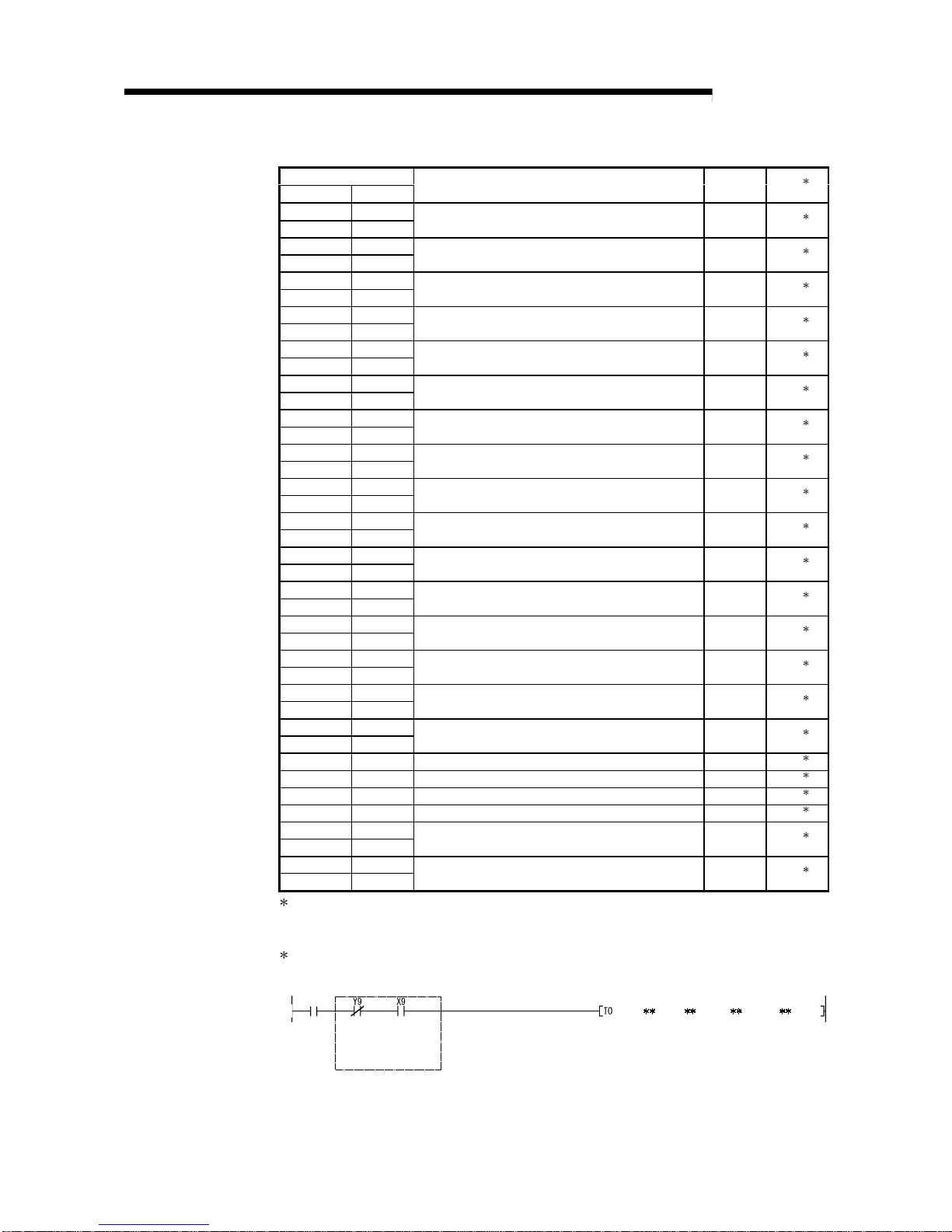
3 - 30 3 - 30
MELSEC-Q
3 SPECIFICATIONS
Table 3.6 Buffer memory assignment o f Q64AD -GH ( 3/5)
Address
Hexadecimal Decimal
Description Default R/W
1
56
H
86
57
H
87
CH1 Process alarm lower lower limit value (L)
(H)
0R/W
2
58
H
88
59
H
89
CH1 Process alarm lower upper limit value (L)
(H)
0R/W
2
5A
H
90
5B
H
91
CH1 Process alarm upper lower limit value (L)
(H)
0R/W
2
5C
H
92
5D
H
93
CH1 Process alarm upper upper limit value (L)
(H)
0R/W
2
5E
H
94
5F
H
95
CH2 Process alarm lower lower limit value (L)
(H)
0R/W
2
60
H
96
61
H
97
CH2 Process alarm lower upper limit value (L)
(H)
0R/W
2
62
H
98
63
H
99
CH2 Process alarm upper lower limit value (L)
(H)
0R/W
2
64
H
100
65
H
101
CH2 Process alarm upper upper limit value (L)
(H)
0R/W
2
66
H
102
67
H
103
CH3 Process alarm lower lower limit value (L)
(H)
0R/W
2
68
H
104
69
H
105
CH3 Process alarm lower upper limit value (L)
(H)
0R/W
2
6A
H
106
6B
H
107
CH3 Process alarm upper lower limit value (L)
(H)
0R/W
2
6C
H
108
6D
H
109
CH3 Process alarm upper upper limit value (L)
(H)
0R/W
2
6E
H
110
6F
H
111
CH4 Process alarm lower lower limit value (L)
(H)
0R/W
2
70
H
112
71
H
113
CH4 Process alarm lower upper limit value (L)
(H)
0R/W
2
72
H
114
73
H
115
CH4 Process alarm upper lower limit value (L)
(H)
0R/W
2
74
H
116
75
H
117
CH4 Process alarm upper upper limit value (L)
(H)
0R/W
2
76
H
118 CH1 Rate alarm warning detection period 0 R/W
2
77
H
119 CH2 Rate alarm warning detection period 0 R/W
2
78
H
120 CH3 Rate alarm warning detection period 0 R/W
2
79
H
121 CH4 Rate alarm warning detection period 0 R/W
2
7A
H
122
7B
H
123
CH1 Rate alarm upper limit value (L)
(H)
0R/W
2
7C
H
124
7D
H
125
CH1 Rate alarm lower limit valu e ( L )
(H)
0R/W
2
1 Indicates whether reading and writing to/from a sequence program are enabled.
R : Read enabled
W : Write enabled
2 When writing data to the buffer memory, always perform write under the interlock conditions (buffer
memory write conditions) of the following I/O signals.
Writing
request
Buffer memory writing conditions
Operating
condition
setting
request
Operating
condition
setting
completed
flag

3 - 31 3 - 31
MELSEC-Q
3 SPECIFICATIONS
Table 3.6 Buffer memory assignment o f Q64AD -GH ( 4/5)
Address
Hexadecimal Decimal
Description Default R/W
1
7E
H
126
7F
H
127
CH2 Rate alarm upper limit value (L)
(H)
0R/W
2
80
H
128
81
H
129
CH2 Rate alarm lower limit valu e ( L )
(H)
0R/W
2
82
H
130
83
H
131
CH3 Rate alarm upper limit value (L)
(H)
0R/W
2
84
H
132
85
H
133
CH3 Rate alarm lower limit valu e ( L )
(H)
0R/W
2
86
H
134
87
H
135
CH4 Rate alarm upper limit value (L)
(H)
0R/W
2
88
H
136
89
H
137
CH4 Rate alarm lower limit valu e ( L )
(H)
0R/W
2
8A
H
138 CH1 Input signal error detection setting value 50 R/W
2
8B
H
139 CH2 Input signal error detection setting value 50 R/W
2
8C
H
140 CH3 Input signal error detection setting value 50 R/W
2
8D
H
141 CH4 Input signal error detection setting value 50 R/W
2
8E
H
142
to to
9D
H
157
System area — —
9E
H
158
9F
H
159
Mode switching setting 0 R/W
2
A0
H
160
to to
C7
H
199
System area — —
C8
H
200 Pass data classification setting
3
0R/W
2
C9
H
201 System area — —
CA
H
202
CB
H
203
CH1 Industrial shipment settings offset value
3
(L)
(H)
0R/W
2
CC
H
204
CD
H
205
CH1 Industrial shipment settings gain value
3
(L)
(H)
0R/W
2
CE
H
206
CF
H
207
CH2 Industrial shipment settings offset value
3
(L)
(H)
0R/W
2
D0
H
208
D1
H
209
CH2 Industrial shipment settings gain value
3
(L)
(H)
0R/W
2
D2
H
210
D3
H
211
CH3 Industrial shipment settings offset value
3
(L)
(H)
0R/W
2
D4
H
212
D5
H
213
CH3 Industrial shipment settings gain value
3
(L)
(H)
0R/W
2
D6
H
214
D7
H
215
CH4 Industrial shipment settings offset value
3
(L)
(H)
0R/W
2
D8
H
216
D9
H
217
CH4 Industrial shipment settings gain value
3
(L)
(H)
0R/W
2
1 Indicates whether reading and writing to/from a sequence program are enabled.
R : Read enabled
W : Write enabled
2 When writing data to the buffer memory, always perform write under the interlock conditions (buffer
memory write conditions) of the following I/O signals.
Writing
request
Buffer memory writing conditions
Operating
condition
setting
request
Operating
condition
setting
completed
flag
3 Areas used to restore the user range settings offset/gain values when online module change is made.
Refer to chapter 7 for details of online module change.

3 - 32 3 - 32
MELSEC-Q
3 SPECIFICATIONS
Table 3.6 Buffer memory assignment o f Q64AD -GH ( 5/5)
Address
Hexadecimal Decimal
Description Default
R/W
1
DA
H
218
DB
H
219
CH1 User range settings offset value
3
(L)
(H)
0R/W
2
DC
H
220
DD
H
221
CH1 User range settings gain value
3
(L)
(H)
0R/W
2
DE
H
222
DF
H
223
CH2 User range settings offset value
3
(L)
(H)
0R/W
2
E0
H
224
E1
H
225
CH2 User range settings gain value
3
(L)
(H)
0R/W
2
E2
H
226
E3
H
227
CH3 User range settings offset value
3
(L)
(H)
0R/W
2
E4
H
228
E5
H
229
CH3 User range settings gain value
3
(L)
(H)
0R/W
2
E6
H
230
E7
H
231
CH4 User range settings offset value
3
(L)
(H)
0R/W
2
E8
H
232
E9
H
233
CH4 User range settings gain value
3
(L)
(H)
0R/W
2
1 Indicates whether reading and writing to/from a sequence program are enabled.
R : Read enabled
W : Write enabled
2 When writing data to the buffer memory, always perform write under the interlock conditions (buffer
memory write conditions) of the following I/O signals.
Writing
request
Buffer memory writing conditions
Operating
condition
setting
request
Operating
condition
setting
completed
flag
3 Areas used to restore the user range settings offset/gain values when online module change is made.
Refer to chapter 7 for details of online module change.

3 - 33 3 - 33
MELSEC-Q
3 SPECIFICATIONS
(2) Buffer memory assignment of Q62AD-DGH
Table 3.7 Buffer memory assignment o f Q62AD - DG H ( 1/3)
Address
Hexadecimal Decimal
Description Default R/W
1
0
H
0 A/D conversion enable/disable setting 0003HR/W
2
1
H
1
CH1 Average time/Average number of times/Move average/
Time constant settings
0R/W
2
2
H
2
CH2 Average time/Average number of times/Move average/
Time constant settings
0R/W
2
3
H
3
4
H
4
System area — —
5
H
5 CH1 A/D conversion starting time setting 30 R/W
2
6
H
6 CH2 A/D conversion starting time setting 30 R/W
2
7
H
7
8
H
8
System area — —
9
H
9 Averaging process specification 0 R/W
2
A
H
10 A/D conversion completed flag 0 R
B
H
11 CH1 Digital output value(16Bit) 0 R
C
H
12 CH2 Digital output value(16Bit) 0 R
D
H
13
to to
12
H
18
System area — —
13
H
19 Error code 0 R
14
H
20 Setting range 0 R
15
H
21 System area — —
16
H
22
Offset/gain setting mode
offset specification
0R/W
17
H
23
Offset/gain setting mode
gain specification
0R/W
18
H
24
to to
1D
H
29
System area — —
1E
H
30 CH1 Maximum value(16Bit) 0 R/W
2
1F
H
31 CH1 Minimum value(16Bit) 0 R/W
2
20
H
32 CH2 Maximum value(16Bit) 0 R/W
2
21
H
33 CH2 Minimum value(16Bit) 0 R/W
2
22
H
34
to to
2E
H
46
System area — —
2F
H
47 Input signal error detection/warning output settings 0333HR/W
2
30
H
48 Warning output flag 0 R
31
H
49 Input signal error detection flag 0 R
32
H
50
to to
35
H
53
System area — —
36
H
54
37
H
55
CH1 Digital output value(32Bit) (L)
(H)
0R
1 Indicates whether reading and writing to/from a sequence program are enabled.
R : Read enabled
W : Write enabled
2 When writing data to the buffer memory, always perform write under the interlock conditions (buffer
memory write conditions) of the following I/O signals.
Writing
request
Buffer memory writing conditions
Operating
condition
setting
request
Operating
condition
setting
completed
flag

3 - 34 3 - 34
MELSEC-Q
3 SPECIFICATIONS
Table 3.7 Buffer memory assignment o f Q62AD - DG H ( 2/3)
Address
Hexadecimal Decimal
Description Default R/W
1
38
H
56
39
H
57
CH2 Digital output value(32Bit) (L)
(H)
0R
3A
H
58
to to
3D
H
61
System area — —
3E
H
62
3F
H
63
CH1 Maximum value(32Bit) (L)
(H)
0R/W
2
40
H
64
41
H
65
CH1 Minimum value(32Bit) (L)
(H)
0R/W
2
42
H
66
43
H
67
CH2 Maximum value(32Bit) (L)
(H)
0R/W
2
44
H
68
45
H
69
CH2 Minimum value(32Bit) (L)
(H)
0R/W
2
46
H
70
to to
55
H
85
System area — —
56
H
86
57
H
87
CH1 Process alarm lower lower limit value (L)
(H)
0R/W
2
58
H
88
59
H
89
CH1 Process alarm lower upper limit value (L)
(H)
0R/W
2
5A
H
90
5B
H
91
CH1 Process alarm upper lower limit value (L)
(H)
0R/W
2
5C
H
92
5D
H
93
CH1 Process alarm upper upper limit value (L)
(H)
0R/W
2
5E
H
94
5F
H
95
CH2 Process alarm lower lower limit value (L)
(H)
0R/W
2
60
H
96
61
H
97
CH2 Process alarm lower upper limit value (L)
(H)
0R/W
2
62
H
98
63
H
99
CH2 Process alarm upper lower limit value (L)
(H)
0R/W
2
64
H
100
65
H
101
CH2 Process alarm upper upper limit value (L)
(H)
0R/W
2
66
H
102
to to
75
H
117
System area — —
76
H
118 CH1 Rate alarm warning detection period 0 R/W
2
77
H
119 CH2 Rate alarm warning detection period 0 R/W
2
78
H
120
79
H
121
System area — —
7A
H
122
7B
H
123
CH1 Rate alarm upper limit value (L)
(H)
0R/W
2
1 Indicates whether reading and writing to/from a sequence program are enabled.
R : Read enabled
W : Write enabled
2 When writing data to the buffer memory, always perform write under the interlock conditions (buffer
memory write conditions) of the following I/O signals.
Writing
request
Buffer memory writing conditions
Operating
condition
setting
request
Operating
condition
setting
completed
flag

3 - 35 3 - 35
MELSEC-Q
3 SPECIFICATIONS
Table 3.7 Buffer memory assignment o f Q62AD - DG H ( 3/3)
Address
Hexadecimal Decimal
Description Default R/W
1
7C
H
124
7D
H
125
CH1 Rate alarm lower limit valu e ( L )
(H)
0R/W
2
7E
H
126
7F
H
127
CH2 Rate alarm upper limit value (L)
(H)
0R/W
2
80
H
128
81
H
129
CH2 Rate alarm lower limit valu e ( L )
(H)
0R/W
2
82
H
130
to to
89
H
137
System area — —
8A
H
138 CH1 Input signal error detection setting value 50 R/W
2
8B
H
139 CH2 Input signal error detection setting value 50 R/W
2
8C
H
140
to to
9D
H
157
System area — —
9E
H
158
9F
H
159
Mode switching setting 0 R/W
2
A0
H
160
to to
C9
H
201
System area — —
CA
H
202
CB
H
203
CH1 Industrial shipment settings offset value
3
(L)
(H)
0R/W
2
CC
H
204
CD
H
205
CH1 Industrial shipment settings gain value
3
(L)
(H)
0R/W
2
CE
H
206
CF
H
207
CH2 Industrial shipment settings offset value
3
(L)
(H)
0R/W
2
D0
H
208
D1
H
209
CH2 Industrial shipment settings gain value
3
(L)
(H)
0R/W
2
D2
H
210
to to
D9
H
217
System area — —
DA
H
218
DB
H
219
CH1 User range settings offset value
3
(L)
(H)
0R/W
2
DC
H
220
DD
H
221
CH1 User range settings gain value
3
(L)
(H)
0R/W
2
DE
H
222
DF
H
223
CH2 User range settings offset value
3
(L)
(H)
0R/W
2
E0
H
224
E1
H
225
CH2 User range settings gain value
3
(L)
(H)
0R/W
2
1 Indicates whether reading and writing to/from a sequence program are enabled.
R : Read enabled
W : Write enabled
2 When writing data to the buffer memory, always perform write under the interlock conditions (buffer
memory write conditions) of the following I/O signals.
Writing
request
Buffer memory writing conditions
Operating
condition
setting
request
Operating
condition
setting
completed
flag
3 Areas used to restore the user range settings offset/gain values when online module change is made.
Refer to chapter 7 for details of online module change.

3 - 36 3 - 36
MELSEC-Q
3 SPECIFICATIONS
3.4.2 A/D conversion enable/disable setting (buffer mem ory address 0: Un\G0)
(1) Sets whether th e ou tp ut o f an A/D conv e r sion valu e is ena bl e d or di sabl ed fo r
each channel.
For the Q62AD-DGH, the A/D conversion enable/disable setting also acts as the
ON/OFF setting of the power supply to the 2-wire transmitter.
(2) It is necessary to set the operating condition setting request (Y9) to ON/OFF in
order to enable the A/D conversion enable/disable setting. (See Section 3.3.2.)
(3) The Q64AD-GH de faul t s to A/D conversion enable on all channels.
(4) The Q62AD-DG H de fa ul t s to A/D conv e r sion di sa bl e on all ch an ne l s.
b15 b14 b13 b12 b11 b10 b9 b8
b7
b6
b5
b4 b3 b2 b1 b0
CH4 CH3 CH2 CH1
000000000000
Q64AD-GH
For Q64AD-GH, information of b4 to b15 is fixed at 0.
For Q62AD-DGH, information of b2 to b15 is fixed at 0.
0: A/D conversion enable
1: A/D conversion disable
Q62AD-DGH
0: A/D conversion enable, power supply ON
1: A/D conversion disable, power supply OFF
Example
When the channels using A/D conversion are 1 and 3, 000AH (10) is stored into the
buffer memory address 0 (Un\G0).
b15
CH4 CH3 CH2 CH1
A00
000AH (10)
0000000000001010
b14 b13 b12 b11 b10 b9 b8 b7 b6 b5 b4 b3 b2 b1 b0
0
3 - 37 3 - 37
MELSEC-Q
3 SPECIFICATIONS
3.4.3 CH Average time/Average number of times/Move average/Time constant settings
(buffer memory addresses 1 to 4: Un\G1 to Un\G4)
(1) Set the average time, average count, move average count or primary delay filter
time constant for each channel specified for averaging processing.
(2) To make the settin g val id , t he oper atin g co ndi ti on set ti ng req ue st (Y9) must be
turned ON/OFF. (Refer to Section 3.3.2.)
(3) 0 is set as the default.
(4) The setting ranges are as follows.
Processing method Setting value
Time averaging
40 to 5000 (ms)
1
Count averaging 4 to 500 (times)
Move averaging 2 to 60 (times)
Primary delay filter
10 to 5000 (ms)
1
1 The value can be set in 1ms increments, but the first digit is discarded and
the value is processed in 10ms increments.
POINT
(1) The channel where the value outside the above setting range has been written
results in an error, the error code is stored into the Error code (buffer memory
address 19: Un\G19), the error flag (XF) turns ON, and the A/D conversion
processing is performed at the pre-error setting.
(2) Since the default setting is 0, change it according to the processing method.
(3) The value, which has been set to the channel specified for sampling
processing, is ignored.
3.4.4 CH A/D conversion starting time setting (buffer memory addresses 5, 6: Un\G5,
Un\G6) (Q62AD-DGH only)
(1) This area is used to set the "time necessary from when the used 2-wire transmitter
powers on until its out put st abilizes" on a channel basis.
(2) To make the settin g val id , t he oper atin g co ndi ti on set ti ng req ue st (Y9) must be
turned ON/OFF. (Refer to Section 3.3.2.)
(3) The setting ran ge i s 0 t o 3276 .7 se cond s (0 to 54 minu t e s and 36.7 se con d s)[0 to
32767].
Set the time in 100ms increments.
Example) When setting the A/D conversion starting time to 5 seconds, store 50
into the buffer memory.
(4) The default is set to 3 seconds [30].
(5) Refer to Section 3.2.5 for details of the A/D conversion starting time setting
function.
POINT
The channel where the value outside the above setting range has been written
results in an error, the error code is stored into the Error code (buffer memory
address 19: Un\G19), the error flag (XF) turns ON, and operation is performed at
the pre-error setting.
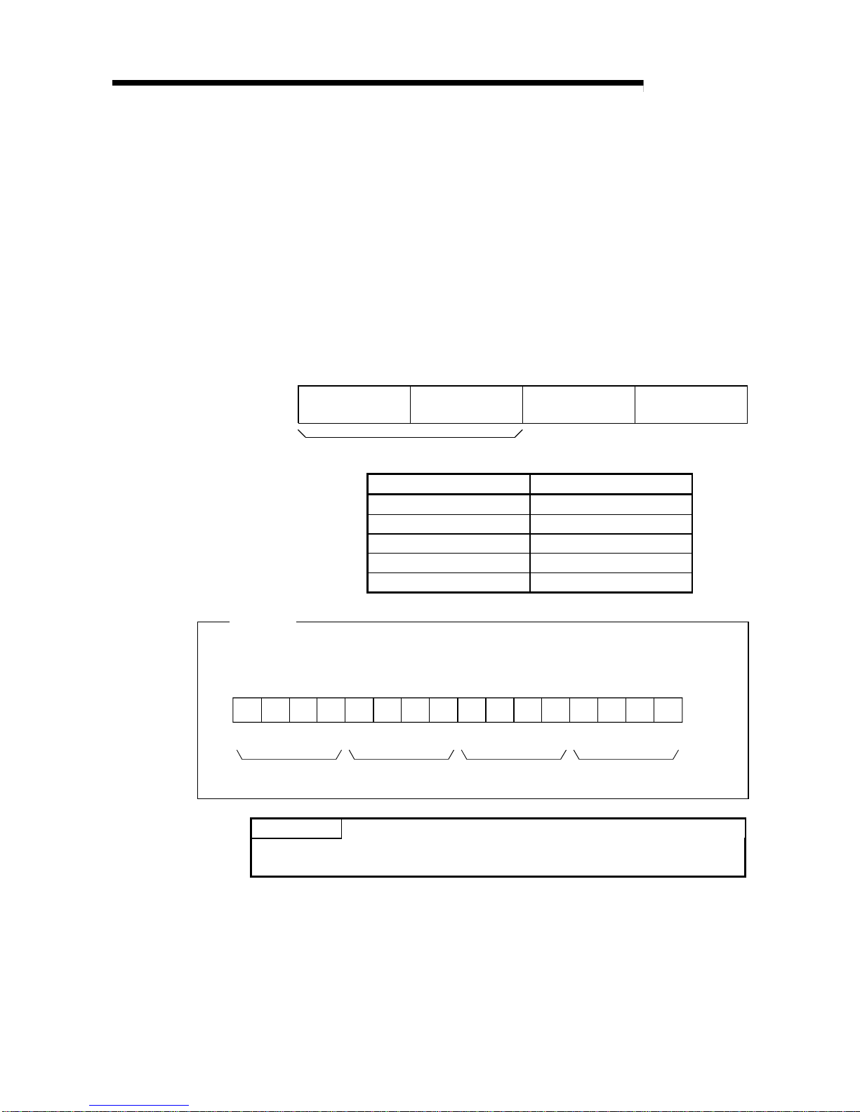
3 - 38 3 - 38
MELSEC-Q
3 SPECIFICATIONS
3.4.5 Averaging process specification (buffer memor y addr ess 9: U n\G9)
(1) When selecting sampling processing or averaging processing, write the setting to
buffer memory address 9 (Un\G9).
(2) When you selected averaging processing, select the average time, average count,
move average or primary delay filter.
(3) To make the settin g val id , t he oper atin g co ndi ti on set ti ng req ue st (Y9) must be
turned ON/OFF. (Refer to Section 3.3.2.)
(4) By default, sampling processing is set for all channels.
b15 b12 b11 b8 b7 b4b3 b0to to to to
CH4 CH3 CH2 CH1
For Q62AD-DGH, information of b8 to b15 is fixed at 0.
Processing method Setting value
Sampling processing 0
H
Time averaging 1
H
Count averaging 2
H
Move averaging 3
H
Primary delay filter 4
H
Example
When setting channel 1 for count averaging, channel 2 for time averaging, channel 3 for
primary delay filt e r, an d ch a nnel 4 fo r sa mpli ng pro ce ssi ng , st ore 41 2 H
(1042) into the
buffer memory address 9 (Un\G9).
b15
CH4 CH3 CH2 CH1
240
412H (1042)
0000010000010010
b14b13b12b11b10b9b8b7b6b5b4b3b2b1b0
1
POINT
For the channel where the value outside the above setting range has been written,
operation is performed by sampling processing.

3 - 39 3 - 39
MELSEC-Q
3 SPECIFICATIONS
3.4.6 A/D conversion completed flag (buffer me mor y addr ess 10: U n\G10)
(1) When A/D conversion for the channels enabled for conversion is complete, the
A/D conversion completed flag is set to 1.
The A/D conversion completed flag (XE) is set to ON when the conversion for all
A/D conversion enabled channels is complete.
(2) When the operating condition setting request (Y9) is set to ON, the flag returns to
the default setting of 0 and changes to 1 when A/D conversion is complete.
b15 b14 b13 b12 b11 b10 b9 b8 b7 b6 b5 b4 b3 b2 b1 b0
CH4 CH3 CH2 CH1
000000000000
For Q64AD-GH, information of b4 to b15 is fixed at 0.
For Q62AD-DGH, information of b2 to b15 is fixed at 0.
1 : A/D conversion completed
0 : A/D conversion in
pro
g
ress or not used
Example
When all conversions of channels 1 and 2 enabled for A/D conversion are completed,
0003H
(3) is stored into the buffer memory address 10 (Un\G10).
b15
CH4 CH3 CH2 CH1
300
0003H (3)0000000000000011
b14 b13 b12 b11 b10 b9 b8 b7 b6 b5 b4 b3 b2 b1 b0
0
3.4.7 CH digital output value (16bit) (buffer memory addresses 11 to 14: Un\G11 to
Un\G14)
(1) The value in the digital output value (32bit) (buffer memory addresses 54 to 61:
Un\G54 to Un\G61) is converted and the result of conversion is stored in 16-bit
signed binary.
b15 b14 b13 b12 b11 b10 b9 b8 b7 b6 b5 b4 b3 b2 b1 b0
Data section
Signed bit
1: Negati ve
0: Positive

3 - 40 3 - 40
MELSEC-Q
3 SPECIFICATIONS
3.4.8 Write data error codes (buffer memory address 19: Un\G19)
(1) The error codes generated by the A/D converter modules are stored here.
(2) See Section 8.1 fo r t he det ail s o f th e e rro r code s.
3.4.9 Setting range (buffer memory addr ess 20: U n\G20)
(1) These areas are used to confirm the setting ranges of the A/D converter module.
(2) The setting value is stored into the buffer memory address 20 (Un\G20).
b15 b12 b11 b8 b7 b4b3 b0to to to to
CH4 CH3 CH2 CH1
For Q62AD-DGH, information of b8 to b15 is fixed at 0.
Setting ranges of Q64AD-GH
Input range Setting value
4 to 20 (mA) 0
H
0 to 20 (mA) 1
H
1 to 5 (V) 2
H
0 to 5 (V) 3
H
-10 to 10(V) 4
H
0 to 10 (V) 5
H
User range setting
(Uni-polar)
E
H
User range setting
(Bi-polar)
F
H
Setting ranges of Q62AD-DGH
Input range Setting value
4 to 20 (mA) 0
H
User range setting F
H

3 - 41 3 - 41
MELSEC-Q
3 SPECIFICATIONS
3.4.10 Offset/gain setting mode (buffer memory addresses 22, 23: Un\G22, Un\G23)
(1) Specifies the channel to be adjusted for the offset/gain settings.
(2) The channel for which the offset is to be adjusted is specified in buffer memory
address 22 (Un\ G22 ) and t h e chan ne l fo r wh i ch th e ga in i s to be adju sted is
specified in buffer memory address 23 (Un\G23).
(3) Although it is po ssi bl e t o set mul t ipl e ch an nel s at th e sa me time, set the offset a n d
gain separately (buffer memory addresses 22, 23: Set either Un\G22 or Un\G23 to
0). If both are set at the same time, an offset/gain setting mode error (error code
500) occurs.
(4) See Section 4.6 for the details of the offset/gain settings.
b15 b14 b13 b12 b11 b10 b9 b8 b7 b6 b5 b4 b3 b2 b1 b0
000000000000000
0
CH4 CH3 CH2 CH1
CH4 CH3 CH2 CH1
0000000
0
Un\G22 (Offset specification)
Un\G23 (Gain specification)
For Q64AD-GH, information of b4 to b15 is fixed at 0.
For Q62AD-DGH, information of b2 to b15 is fixed at 0.
1 : Channel to be set
0 : Invalid
3.4.11 CH maximum value/minimum value storage area ( 16bit) ( buffer mem or y addr esses
30 to 37: Un\G30 to Un\G37)
(1) The value in the maximum value/minimum value storage area (32bit) (buffer
memory addresses 62 to 77: Un\G62 to Un\G77) is converted and the result of
conversion is stored in 16-bit signed binary.
(2) The stored values for all channels will be cleared to 0 when the operating
condition setting request (Y9) is set to ON and the setting is changed or when the
maxi mum value/ minimum val ue reset request (YD) i s s e t to ON.
(3) The maximum and minimum values are stored for each sample processing time
(measurement), even with channels for which averaging processing is specified.

3 - 42 3 - 42
MELSEC-Q
3 SPECIFICATIONS
3.4.12 Input signal error detection/warning output settings (buffer memory address 47:
Un\G47)
(1) This area is used to set whether the input signal error detection/process alarm/rate
alarm warning will be output or stopped on a channel basis.
(2) To make the input sig n al e rro r de tect io n/w a rni ng ou tput set ti ng s vali d, th e
operating condition setting request (Y9) must be turned ON/OFF. (Refer to
Section 3.3.2.)
(3) By default, all channels are set to disable.
b15 b14 b13 b12 b11 b10 b9 b8 b7 b6 b5 b4 b3 b2 b1 b0
CH4 CH3 CH2 CH10 0 0 0 CH4 CH3 CH2 CH1CH4 CH3 CH2 CH1
Information of b12
to b15 is fixed at 0.
Input signal error detection Rate alarm setting Process alarm setting
0: Enable, 1: Disable
For Q62AD-DGH, information of b2, b3, b6, b7, b10 and b11 is fixed at 0.
Example
When channel 1 is enabled for process alarm warning output and channel 3 is enabled for
input signal error detection, 0BFEH
(3070) is stored into the buffer memory address 47
(Un\G47).
b15
CH4 CH3 CH2 CH1
EB0
0BFEH (3070)0000101111111110
b14b13b12b11b10b9b8b7b6b5b4b3b2b1b0
F
CH4 CH3 CH2 CH1CH4 CH3 CH2 CH1
3.4.13 Warning output flag (buffer memor y address 48 :Un\G48)
(1) If the digital output value or its varying rate falls outside the setting range set to the
CH
process alarm upper/lower limit value (buffer memory addresses 86 to 117:
Un\G86 to Un\G117) or CH
rate alarm upper/lower limit value (buffer memory
addresses 122 to 137: Un\G122 to Un\G137), the warning output flag for the
corresponding channel turns to 1.
(2) For both the process alarm and rate alarm, whether the warning is for the upper or
lower limit value can be checked on a channel basis.
(3) When the digital output value or its varying rate returns to within the setting range,
the warning output flag is automatically reset.
(4) If the warning is detected on any one of the channels enabled for A/D conversion
and enabled for process alarm or rate alarm warning output, the Warning output
signal (X8) also turns ON.
(5) When the operating condition setting request (Y9) is turned ON, the warning
output flag is cleared.
b15 b14 b13 b12 b11 b10 b9 b8 b7 b6 b5 b4 b3 b2 b1 b0
CH2 CH2 CH1 CH1CH4 CH4 CH3 CH3CH2 CH2 CH1 CH1CH4 CH4 CH3 CH3
Lower
limit
value
Upper
limit
value
Lower
limit
value
Upper
limit
value
Lower
limit
value
Upper
limit
value
Lower
limit
value
Upper
limit
value
Lower
limit
value
Upper
limit
value
Lower
limit
value
Upper
limit
value
Lower
limit
value
Upper
limit
value
Lower
limit
value
Upper
limit
value
Rate alarm Process alarm
0: Normal, 1: Alarm ON
For Q62AD-DGH, information of b4 to b7 and b12 to b15 is fixed at 0.

3 - 43 3 - 43
MELSEC-Q
3 SPECIFICATIONS
3.4.14 Input signal error detection flag ( buffer me mor y addr ess 49: U n\G49)
(1) If the analog inpu t valu e de te cted fal ls outside the setting ra nge se t to th e C H
input signal error detection setting value (buffer memory addresses 138 to 141:
Un\G138 to Un\G141), the Input signal error detection flag for the corresponding
channel turns to 1.
(2) By bringing the analog input value within the setting range and then turning ON
the Error clear request (YF), the Input signal error detection flag turns OFF.
(3) If the warning is detected on any one of the channels enabled for input signal error
detection and en abl ed fo r A /D conversion, the Input signal err o r det e ctio n sig na l
(XC) also turns ON.
(4) When the operating condition setting request (Y9) is turned ON, the Input signal
error detection flag is cleared.
b15 b14 b13 b12 b11 b10 b9 b8 b7 b6 b5 b4 b3 b2 b1 b0
CH4 CH3 CH2 CH1
000000000000
For Q64AD-GH, information of b4 to b15 is fixed at 0.
For Q62AD-DGH, information of b2 to b15 is fixed at 0.
0: Normal
1: Input signal error
3.4.15 CH digital output value (32bit) (buffer memory addresses 54 to 61: Un\G54 to
Un\G61)
(1) The digital output values converted from analog to digital are stored into the buffer
memory addresses 54 to 61 (Un\G54 to Un\G61) channel by channel.
(2) The digital ou tp ut valu e is rep re se nt ed in 32 - bi t sign ed bina ry. (The data part is 16
bits long.)
b31 b24b23 b16b15 b8 b7 b0
Signed bit
1: Negative
0: Positive
Data section
Bits other than data section and signed bit are 1 when value
is negative (1 in b31) or 0 when value is positive (0 in b31).

3 - 44 3 - 44
MELSEC-Q
3 SPECIFICATIONS
3.4.16 CH maximum value/minimum value storage area ( 32bit) ( buffer mem or y addr esses
62 to 77: Un\G62 to Un\G77)
(1) The maximum valu e an d minimum value of the digit al val ue conv e r ted on a
channel basis are stored in 32-bit signed binary. (The data part is 16 bits long.)
(2) The stored values for all channels will be cleared to 0 when the operating
condition setting request (Y9) is set to ON and the setting is changed or when the
maxi mum value/ minimum val ue reset request (YD) i s s e t to ON.
(3) The maximum and minimum values are stored for each sample processing time
(measurement), even with channels for which averaging processing is specified.
3.4.17 CH process alarm upper/lower limit value (buffer memory addr esses 86 to 117:
Un\G86 to Un\G117)
(1) Set the range of the digital output value on a channel basis.
(2) To make the settin g val id , t he oper atin g co ndi ti on set ti ng req ue st (Y9) must be
turned ON/OFF. (Refer to Section 3.3.2.)
(3) The setting ran ge is - 65 536 to 65 53 5.
Make settings in four stages: process alarm upper upper limit value, upper lower
limit value, lower upper limit value and lower lower limit value.
(4) The channel, where the value outside the above setting range has been set or the
value that does not satisfy the condition of lower lower limit value
lower upper
limit value upper lower limit value upper upper limit value has been set,
results in an error, the error code is stored into the error code (buffer memory
address 19: Un\G19), the error flag (XF) turns ON, and operation is performed at
the pre-error setting.
(5) Refer to Section 3.2.4 for details of the process alarm.

3 - 45 3 - 45
MELSEC-Q
3 SPECIFICATIONS
3.4.18 CH rate alarm warning detection period (buffer memory addresses 118 to 121:
Un\G118 to Un\G121)
(1) Set the period, at which the varying rate of the digital output value will be checked,
on a channel basis.
(2) To make the settin g val id , t he oper atin g co ndi ti on set ti ng req ue st (Y9) must be
turned ON/OFF. (Refer to Section 3.3.2.)
(3) The setting range is 10 to 5000ms.
The value can be set in 1ms increments, but the first digit is discarded and the
value is processed in 10ms increments.
(4) When time averaging or count averaging has been specified for averaging
process specification, set the rate alarm warning detection period as a multiple of
the time averaging or count averaging conversion period.
Example) When the count setting of count averaging is 20 times, the conversion
period is 200ms. Therefore, set a multiple of 200, e.g. 400 or 600.
20 (times)
10 (ms) = 200 (ms)
(5) The default set tin g i s 0ms.
(6) Refer to Section 3.2.4 for details of the rate alarm.
POINT
(1) The channel where the value outside the above setting range has been written
results in an error, the error code is stored into the Error code (buffer memory
address 19: Un\G19), the error flag (XF) turns ON, and the time averaging or
count averaging processing and rate alarm are executed at the pre-error
setting.
(2) Since the defa ul t set ti n g is 0, chan ge th e se ttin g.
(3) If the upper limit value and lower limit value settings of the rate alarm are
small, the warning output may turn ON due to overreaction to disturbance or
like. In this case, overreaction to disturbance or like can be avoided by
increasing the se tt in g of th e rate ala r m wa rning de te cti on pe riod .

3 - 46 3 - 46
MELSEC-Q
3 SPECIFICATIONS
3.4.19 CH rate alarm upper/lower limit value (buffer memory addresses 122 to 137:
Un\G122 to Un\G137)
(1) Set the varying rate range of the digital output value on a channel basis.
(2) To make the settin g val id , t he oper atin g co ndi ti on set ti ng req ue st (Y9) must be
turned ON/OFF. (Refer to Section 3.3.2.)
(3) The setting range is -65536 to 65535 (-6553.6 to 6553.5%). Set the value in
0.1%/s increments.
Example) When setting the rate alarm upper limit value to 30%/s, store 300 into
the buffer memory.
(4) Refer to Section 3.2.4 for details of the rate alarm.
POINT
The channel where the value outside the above setting range has been written
results in an error, the error code is stored into the Error code (buffer memory
address 19: Un\G19), the error flag (XF) turns ON, and the rate alarm is executed
at the pre-error setting.
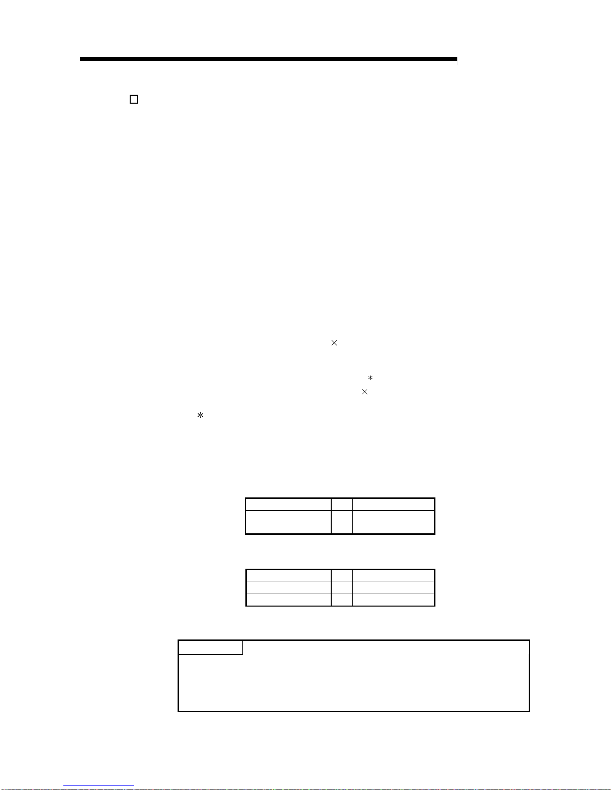
3 - 47 3 - 47
MELSEC-Q
3 SPECIFICATIONS
3.4.20 CH input signal error detection setting value (buffer memory addresses 138 to 141:
Un\G138 to Un\G141)
(1) Set the value, a t wh i ch th e e rro r o f th e en te re d an al og value wi ll be de te ct e d, on a
channel basis.
(2) To make the setting valid, the Operating condition setting request (Y9) must be
turned ON/OFF. (Refer to Section 3.3.2.)
(3) The setting range is 0 to 250 (0 to 25.0%). Set the value in 0.1% increments.
Example) When setting the input signal error detection setting value to 15%, store
150 into the buffer memory.
(4) The input signal error detection upper and lower limit values depend on the used
range.
The expressions for calculating the input signal error detection upper and lower
limit values are as follows.
Input signal err o r dete ctio n up pe r limit value
= gain value of corresponding range + (gain value of corresponding range - offset
value of corresponding range)
(setting value/1000)
Input signal error detection lower limit value
= lower limit value of correspo nding range
+ (gain value of corresponding range
- offset value of corresponding range)
(setting value/1000)
When the user range setting is used, the lower limit value is as follows.
Example) Lower l i mit value w hen th e ga in value se tt in g i s 8V and th e o ffse t
value setting is 4V
For the user range setting (uni-polar) of the Q64AD-GH or the user
range setting of the Q62AD-DGH, the offset value is the lower limit
value.
Gain value 8V 64000
Offset value
(Lower limit value)
4V 0
For the user range setting (bi-polar), the analog value corresponding
to the digital value of -64000 is the lower limit value.
Gain value 8V 64000
Offset value 4V 0
Lower limit value 0V -64000
(5) Refer to Section 3.2.3 for details of the input signal error detection function.
POINT
(1) Set the input signa l e rr or de te ctio n up pe r limit value to less than 25 mA.
If the setting is 25mA or more, the error may not be detected.
(2) For the Q62AD-D GH, set th e in pu t si gn al err or de te ctio n low e r li mi t valu e t o
0mA or more.
If it has been set to l e ss than 0mA, th e e rr o r may no t be de te ct ed .

3 - 48 3 - 48
MELSEC-Q
3 SPECIFICATIONS
3.4.21 Mode switching setting (buffer memory addr esses 158, 159: U n\G15 8, Un\G159)
(1) Set the values of the mode desired to be switched to.
(2) After setting the values, turning the operating condition setting request (Y9) from
OFF to ON switches to that mode.
(3) When mode switching is performed, this area is cleared to zero and the operating
condition setting completed flag (X9) turns OFF.
After confirming that the operating condition setting completed flag (X9) has
turned OFF, turn OFF the operating condition setting request (Y9).
Set values
Mode to be switched to
Buffer memory address 158 Buffer memory address 159
Normal mode 0964
H
4144
H
Offset/gain setting mode 4144
H
0964
H
POINT
If the values written are other than the above, mode switching is not performed and
only the operating condition is changed.
3.4.22 Pass data classification setting (buffer memory addr esses 200: Un\G200)
(Q64AD-GH only)
(1) Areas used to restore the user range settings offset/gain values when online
module change is made.
Refer to chapter 7 for details of online module change.
(2) Specify whether the offset/gain values to be saved/restored are voltages or
currents when saving/restoring the offset/gain values of the user range setting.
b15 b14 b13 b12 b11 b10 b9 b8
b7
b6
b5
b4 b3 b2 b1 b0
CH4 CH3 CH2 CH1
00000000
Information of b4 to b15 is fixed to 0. 1: Current specified
0: Voltage specified
0000
POINT
Refer to Section 4.6 for the offset/gain value setting method.

3 - 49 3 - 49
MELSEC-Q
3 SPECIFICATIONS
3.4.23 Industrial shipment settings and user rang e setti ng s offset/gain value (buffer memory
addresses 202 to 233: Un\G202 to Un\G233)
(1) Areas used to restore the user range settings offset/gain values when online
module change is made.
Refer to chapter 7 for details of online module change.
(2) When the offset/gain values of the user range setting are restored, the used data
are stored.
The data are stored (saved) when:
• Initial setting write is performed by the utility;
• The operating condition is set (Y9 turns from OFF to ON
1); or
• The offset/gain values are written in the offset/gain setting mode (YA turns from
OFF to ON).
1: The data are not saved when values have been written to the mode
switching setting area (buffer memory addresses 158, 159: Un\G158,
Un\G159).
(3) When restoring the offset/gain values of the user range setting, set the data saved
here similarly into the corresponding area of the module where the data will be
restored.
(4) Buffer memory saving recording procedure for online module change
1) Set the pass data classification setting
(buffer memory addresses 200:
Un\G200).
2) Turn the operating condition setting request (Y9) from OFF to ON.
3) Compare the offset/gain values of the industrial shipment settings and user
range settings (buffer memory addresses 202 to 233: Un\G202 to Un\G233)
with the range reference values. Refer to Section 7.4 for the range reference
values.
4) If the values are proper, record the values of the pass data classification
setting
, industrial shipment settings and user range settings offset/gain value.
: The Q62AD-DGH does not require the setting and recording of the pass data
classification setti ng .
POINT
Refer to Section 4.6 for the offset/gain value setting method.

4 - 1 4 - 1
MELSEC-Q
4 SETUP AND PROCEDURES BEFORE OPERATION
4 SETUP AND PROCEDURES BEFORE OPERATION
4.1 Handling Precautions
(1) Do not drop the module or subject it to heavy impact.
(2) Do not remove the PCB of the module from its case.
Doing so may cause the module to fail.
(3) Be careful not to let foreign particles such as swarf or wire chips enter the module.
They may cause a fire, mechanical failure or malfunction.
(4) The top surface of the module is covered with a protective film to prevent foreign
objects such as wire burrs from entering the module during wiring.
Do not remove this film until the wiring is complete.
Before operating the system, be sure to remove the film to provide adequate
ventilation.
(5) Tighten the terminal screws using torque within the following ranges. Loose
screws may cause short circuits, mechanical failures or malfunctions.
Screw location Clamping torque range
Module mounting screws (M3 screws) 0.36 to 0.48 N.m
Terminal block screws (M3 screws) 0.42 to 0.58 N.m
Terminal block mounting screws (M3.5 screws) 0.66 to 0.89 N.m
(6) To mount the module on the base unit, fully insert the module fixing latch into the
fixing hole in the base unit and press the module using the hole as a fulcrum.
Improper installation may result in a module malfunction, or may cause the
module to fall off.
4

4 - 2 4 - 2
MELSEC-Q
4 SETUP AND PROCEDURES BEFORE OPERATION
4.2 Setup and Procedures before Operation
Start
Wiring
Wire external devices to the A/D converter module.
Intelligent func t ion modul e s w itc h s ett i ng s
Perform settings using GX Developer
(see Section 4.5).
Use user range settings?
Offset/gain setting
If user range settings are used, perform the
offset and gain settings (see Section 4.6).
Use the utility pac k ag e ?
Initial setting and automatic refresh setting
The program can be simp lif ie d if t h e utility
package is used for setting (see Chapter 5).
Programming and debugging
Create and check the sequence program.
Use industrial shipment
settings
Use user range settings
NO
YES
Module mounting
Mount the A/D converter module in the specified
slot.
4

4 - 3 4 - 3
MELSEC-Q
4 SETUP AND PROCEDURES BEFORE OPERATION
4.3 Part Identification Nomenclature
The name of each part of the A/D converter module is listed below.
1)
2)
3)
1
2
3
4
5
6
7
8
9
10
11
12
13
14
15
16
RUN
ERR.
A/D
-10 10V
0 20mA
Q64AD-GH
17
18
ALM
V+
C
H
2
C
H
3
C
H
4
V-
I+
SLD
V+
V-
I+
SLD
V+
V-
I+
SLD
V+
V-
I+
SLD
C
H
1
Q64AD-GH Q62AD-DGH
1
2
3
4
5
6
7
8
9
10
11
12
13
14
15
16
RUN
ERR.
Q62AD-DGH
17
18
ALM
CH1
P
I/CHK+
CHK-
CH2
P
I/CHK+
CHK-
1)
2)
3
)
4)
5)
IN
24VDC
(FG)
4 20mA
Number
Name and
appearance
Description
1) RUN LED
Displays the operating status of the A/D converter module.
On : Normal operation
Flickering : During offset/gain setting mode
Off : 5V power supply interrupted, watch dog timer
error or module exchangeable status during
online module change bled
2) ERR. LED
Displays the error status of the A/D converter module.
On : Error
(A/D conversion continues.)
Flickering : Error
(A/D conversion stops.)
Off : Normal operation
3) ALM LED
Displays the warning status of the A/D converter module.
On : An alarm (process alarm, rate alarm) is being
generated.
Flickering : An input signal error is being generated.
Off : Normal operation
4)
Check terminals
(Q62AD-DGH only)
Terminal used to check the analog input current value.
(See Section 4.4.2)
5)
External supply
power terminal
(Q62AD-DGH only)
Terminal to connect 24VDC external supply power.
Check the error code for details.
POINT
When two or more errors have occurred, the latest error found by the A/D converter
module is displayed on the LED.
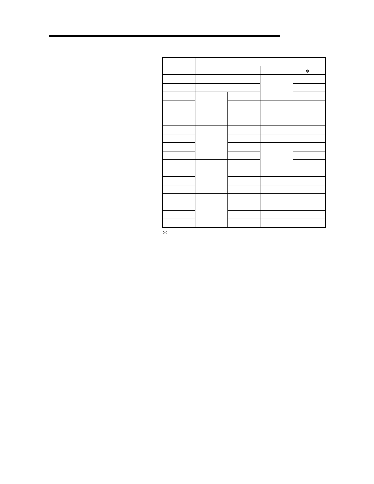
4 - 4 4 - 4
MELSEC-Q
4 SETUP AND PROCEDURES BEFORE OPERATION
Signal name
Terminal
number
Q64AD-GH Q62AD-DGH
1Empty P
2 Empty I/CHK +
3V +
CH1
CHK –
4 V – Empty
5 I + Empty
6
CH1
SLD Empty
7 V + Empty
8 V – Empty
9I +P
10
CH2
SLD I/CHK +
11 V +
CH2
CHK –
12 V – Empty
13 I + Empty
14
CH3
SLD Empty
15 V + Empty
16 V – 24V
17 I + 24G
18
CH4
SLD FG
P : Power supply for 2-wire transmitter
I/CHK + : 2-wire transmitter current input/check (+) terminal
CHK – : Check (–) terminal

4 - 5 4 - 5
MELSEC-Q
4 SETUP AND PROCEDURES BEFORE OPERATION
4.4 Wiring
The wiring precautions and examples of module connection are provided below.
4.4.1 Wiring precautions
In order to optimize the functions of the A/D converter module and ensure system
reliability, external wiring that is protected from noise is required.
Please observe the following precautions for external wiring:
(1) Use separate cables for the AC control circuit and the external input signals of the
Q64AD-GH to avoid the influence of the AC side surges and inductions.
(2) Use separate cables for the AC control circuit and the external input signals and
external supply power of the Q62AD-DGH to avoid the influence of the AC side
surges and inductions.
(3) Do not mount the cables close to or bundle them with the main circuit line, a high-
voltage cable or a load cable from other than the PLC.
This may increase the effects of noise, surges and induction.
(4) Perform an one-point grounding for shielded lines and the shields of sealed
cables.
(5) A solderless terminal with insulating sleeve cannot be used for the terminal block.
Covering the cable-connection portion of the solderless terminal with a marked
tube or an insulation tube is recommended.

4 - 6 4 - 6
MELSEC-Q
4 SETUP AND PROCEDURES BEFORE OPERATION
4.4.2 External wiring
(1) Q64AD-GH
V+
I+
V-
SLD
GND
*1
*4
*2
500k
500k
Shielded
+
-
V+
I+
V-
SLD
Shielded
Signal source 0 to 10V
(a) For voltage input
V+
I+
V-
SLD
GND
*1
*4
*2
250
+
-
500k
500k
Shielded
*3
Signal source 0 to 20V
(b) For current input
*1 Use a 2-core twisted shielded wire for the power wire.
*2 Shows input resistance.
*3 For current input, be sure to connect to (V+) and (I+) terminals.
*4 Be sure to ground the shield wire of each channel.
The SLD terminal can be used when grounding, however it has not been wired inside the board.
Ground it as shown in the diagram shown above or below.
In addition, ground the FG of the power supply module.

4 - 7 4 - 7
MELSEC-Q
4 SETUP AND PROCEDURES BEFORE OPERATION
(2) Q62AD-DGH
V+
V-
V
P
I/CHK+
CHK-
24V
24G
24V
24G
DC24V
*4
*5
*2
250
*3
24V
24G
FG
(4 to 20mA)
2-wire
transmitter
+
-
Current
limiting circuit
Insulating
circuit
Transmitter
power supply
Filter
*1 Shielded
*1 Use a 2-core twisted shielded wire for the power wire.
*2 Shows input resistance.
*3 To connect with the 2-wire transmitter, be sure to connect to P and I/CHK+.
*4 Always use a ground. In addition, ground the FG of the power supply module.
*5 The check terminals (I/CHK+, CHK-) are used to check the amount of input
in mA in relation to the 2-wire transmitter output.
This can be checked since analog inputs of 4 to 20mA are converted to analog outputs of 1 to 5V.
The relationship of this conversion can be expressed by the following formula:
1000
250
Analog output (V) =
Analog input (mA)
IMPORTANT
Q62AD-DGH needs to powered on 30 minutes prior to operation for compliance to
the specification (accuracy).
Therefore, power on 30 minutes prior to offset/gain setting or after online module
change.
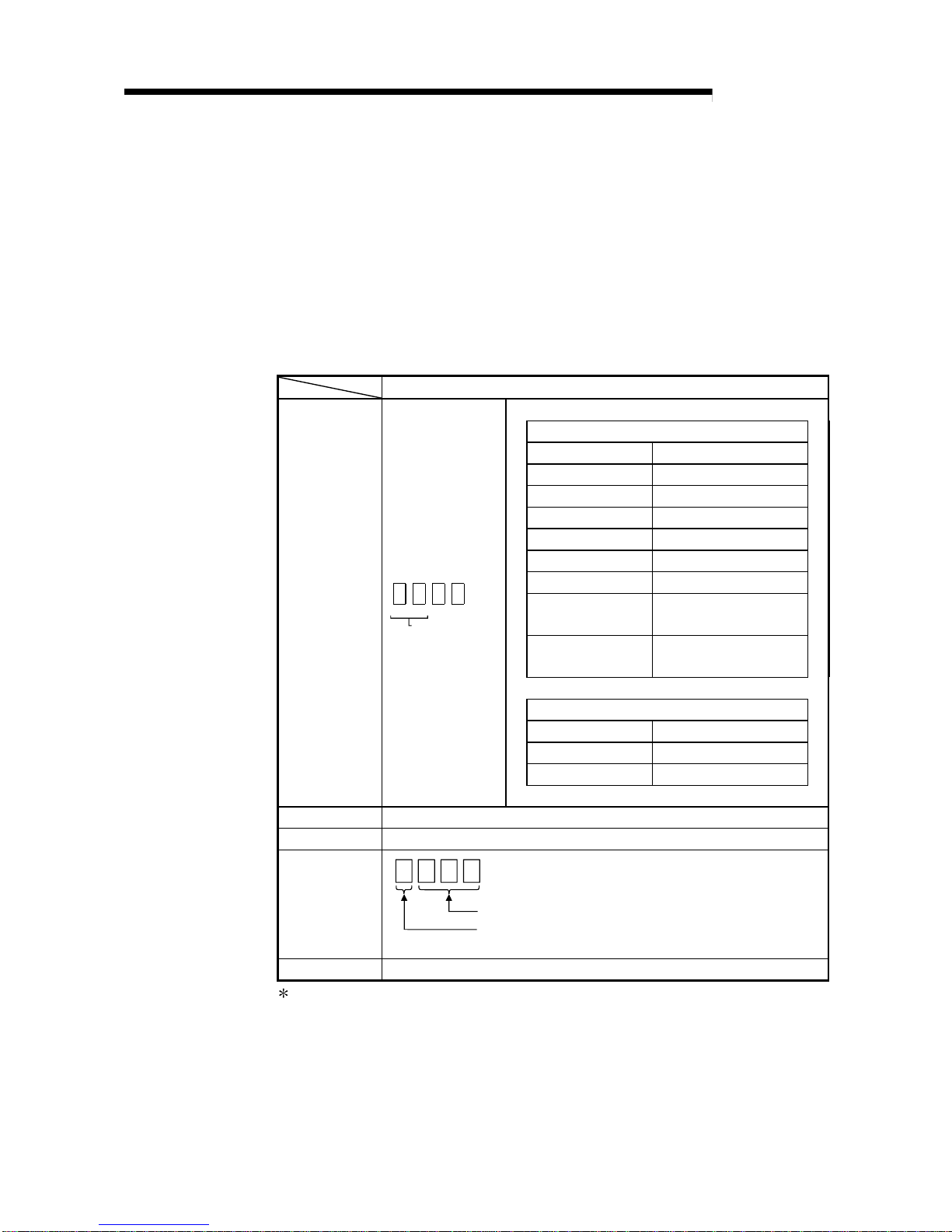
4 - 8 4 - 8
MELSEC-Q
4 SETUP AND PROCEDURES BEFORE OPERATION
4.5 Switch Setting for Intelligent Function Modul e
The settings for the intelligent function module are performed using the I/O assignment
settings for GX Developer.
(1) Setting item
The intelligent function module switches consist of switches 1 to 5 and are set
using 16 bit data. When the intelligent function module switches are not set, the
default value for switches 1 to 5 is 0.
Table 4.1 Switch setting item
Setting item
Q64AD-GH
Analog input range Input range setting v alue
4 to 20 mA 0
H
0 to 20 mA 1
H
1 to 5 V 2
H
0 to 5 V 3
H
– 10 to 10 V 4
H
0 to 10 V 5
H
User range setting
(Uni-polar)
E
H
User range setting
(Bi-polar)
F
H
Q62AD-DGH
Analog input range Input range setting v alue
4 to 20 mA 0
H
User range setting F
H
Switch 1
Input range setting
CH4CH3 CH2 CH1
H
Fixed at 0 0
H
for Q62AD-DGH
Switch 2 Empty
Switch 3 Empty
Switch 4
0H : Normal mode (A/D conversion processing)
1 to F
H
(numeric value other than 0H)* : Offset/gain setting mode
H
000H Fixed
Switch 5 0 : Fixed
Setting any value withi n t h e set ti ng rang e wi ll provi de th e sa me op er at ion .
When the setting range is 1 to F
H
, set 1 for example.

4 - 9 4 - 9
MELSEC-Q
4 SETUP AND PROCEDURES BEFORE OPERATION
(2) Operating procedure
Start the settings with GX Developer I/O assignment setting screen.
(a) I/O assignment setting screen
Set the follow ing fo r th e slot in w hi ch th e A/ D
converter module is mounted.
The type setting is required; set other items as
needed.
Type : Select "intelli."
Model name : Enter the module model name.
Points : Select 16 points.
Start : Enter the start I/O number for
the A/D converter module.
Detailed setting: Specify the control PLC for the
A/D converter module.
It is unnecessary to set the
"Error time output mode" or
"H/W error time PLC operation
mode" since these settings are
invalid for the A/D converter
module.
(b) Switch setting for intelligent function module
screen
Click on [Switch setting] on the I/O assignment
setting screen to di spl ay the scr een shown at
left, then set switches 1 to 5.
The switches can easily be set if values are
entered in hexadecimal. Change the entry
format to hexadecimal and then enter the
values.

4 - 10 4 - 10
MELSEC-Q
4 SETUP AND PROCEDURES BEFORE OPERATION
4.6 Offset/Gain Settings
When using the user range setting, make the offset/gain setting according to the
operation indicated in Section 4.6.1 or Section 4.6.2.
When the industrial shipment setting is used, offset/gain setting is not necessary.
If the utility package is installed, perform the offset/gain settings according to the
procedure described in Section 5.6.2.
4.6.1 Offset/Gain Settings (Q64AD-GH)
(1) Offset/gain setting procedure
Start
Verify that the mode is set
to offset/gain setting and
the RUN LED is flashing.
Add the voltage or current
that will be the offset value.
Set the offset setting
channel in buffer memory
address 22 (Un\G22).
Set buffer memory address
23 (Un\G23) to 0.
Turn the channel change
request (YB) to ON.
Set the channel change
request (YB) to ON.
Verify that the channel
change completed flag
(XB) is ON.
Adjust other
channels?
YES
NO
Set the channel change
request (YB) to OFF.
Set the channel change
request (YB) to OFF.
Set the offset/gain setting
request (YA) to ON and
perform the offset/gain
settings.
Register to the Q64AD-GH.
After verifying that the offset/
gain setting mode status flag
(XA) is OFF, turn YA OFF.
Verify that the offset/gain
setting mode status flag
(XA) is ON.
Add the voltage or current
that will be the gain value.
Set the gain setting channel
in buffer memory address 23
(Un\G23). Set buffer memory
address 22 (Un\G22) to 0.
ERR. LED lit?
YES
NO
End
Verify that the channel
change completed flag
(XB) is ON.
2)
1)
2)
1
)
Switch to the normal
setting mode.
1
Switch to the offset/gain
setting mode.
1

4 - 11 4 - 11
MELSEC-Q
4 SETUP AND PROCEDURES BEFORE OPERATION
1 The mode switching (normal mode to offset/gain setting mode to normal mode)
method is given below.
• Dedicated instruction (G.OFFGAN) ........... Refer to Section 4.6.1 (2), (a)
• Setting made to mode switching setting (buffer memory addresses 158, 159:
Un\G158, Un\G159) and turning the operation condition setting request (Y9) from
OFF to ON ...................................................Refer to Section 4.6.1 (2), (b)
• Intelligent fu n cti on mod ul e swi t ch se ttin g ...Refer to Section 4.5 , Section 4.6.1 (2), (c)
(After intelligent function module switch setting, reset the PLC CPU or switch power
OFF, then ON.)
POINT
(1) Perform the offset/gain settings in the range that satisfies the conditions
specified in POINT of Section 3.1.2 (1).
When the setting exceed s thi s range, the maximum re sol ution or total accur acy
may not be withi n the range i ndi cat ed in th e pe r forman ce spe ci fi cation .
(2) Though the offset/gain settings can be performed on multiple channels at the
same time, set the offset and gain separately (0 at either of the buffer memory
addresses 22, 23).
If channels are set at the buffer memory addresses 22 (Un\G22) and 23
(Un\G23) at the same time, an error will occur and the ERR. LED will be lit.
(3) After the offset/gain settings are completed, verify that the offset and gain
values have been set correctly under actual usage conditions.
(4) The offset and ga in val ue s ar e sto re d into th e E
2
PROM and are not erased at
power-off.
(5) At the time of offset/gain setting, turn ON the user range write request (YA) to
write the val ue s to the E
2
PROM.
Data can be written to the E
2
PROM up to 100 thousand ti mes.
To prevent accidental write to the E
2
PROM, an error will occur and the error
code (buffer memory address 19: Un\G19) will be stored if write is performed
26 consecutive times.
(6) If an error (error code: 40
1
) occurs during offset/gain setting, re-set the
correct offset/gain value.
The offset/gain value of the channel where the error has occurred is not written
to the module.(
1:
indicates the corresponding channel number.)
(7) Module ready (X0) turns from OFF to ON when the offset/gain setting mode
switches to the normal mode by the dedicated instruction (G.OFFGAN) or the
setting of the mode switching setting (buffer memory addresses 158, 159:
Un\G158, Un\G159).
Note that initial setting processing will be executed if there is a sequence
program that makes initial setting when module ready (X0) turns ON.
(8) Buffer memory add r esse s 20 0 (Un \G20 0 ), 20 2 t o 2 33 (U n \G202 t o U n \ G233 )
are the areas used to restore the user range settings offset/gain values when
online module change is made.
Refer to chapter 7 for details of online module change.
(2) Program examples
The program in the dotted area of (a) is common to (a), (b) and (c).
Is this example, the I/O signals for the Q64AD-GH are X/Y0 to X/YF
• Channel selection..................................................................................M0
• Offset setting..........................................................................................M1
• Gain setting............................................................................................M2
• Channel change command ...................................................................M3
• Offset/gain setting value write command to the module......................M4
• Mode switching......................................................................................M5
• Channel designation storage device.....................................................D0
• Dedicated instruction (G.OFFGAN) setting storage device.................D1
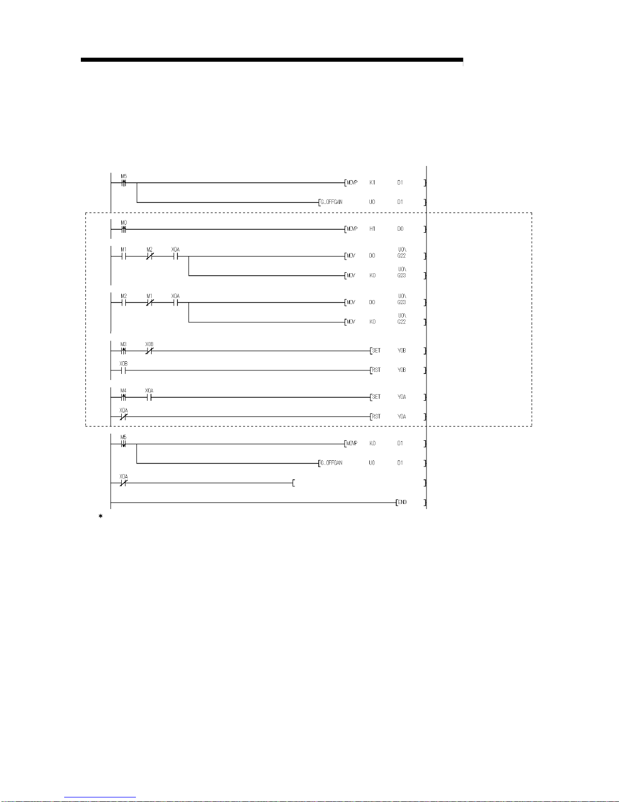
4 - 12 4 - 12
MELSEC-Q
4 SETUP AND PROCEDURES BEFORE OPERATION
(a) When switching the mode using the dedicated instruction (G.OFFGAN)
The following program switches to the offset/gain setting mode with the
dedicated instruction (G.OFFGAN), changes the channel where offset/gain
setting will be made, writes the offset/gain values to the Q64AD-GH, and
then switches to the normal mode.
Stores setting of dedicated
instruction (G.OFFGAN) into D1.
Stores channel where offset/
gain setting will be made into D0.
Specifies offset setting channel.
Sets 0 to buffer memory
address 23.
Specifies gain setting channel.
Sets 0 to buffer memory
address 22.
Turns ON channel change
request (YB).
Turns OFF channel change
request (YB).
Turns ON user range change
request (YA).
Turns OFF user range change
request (YA).
Stores setting of dedicated
instruction (G.OFFGAN) into D1.
Dedicated instruction (G.OFFGAN)
Switches to offset/gain setting mode
Specifies channel where offset/gain setting will be made
Specifies channel where offset setting will be made
Specifies channel where gain setting will be made
Changes channel where offset/gain setting will be made
Registers offset/gain setting results to module
Switches to normal mode
Processing in normal mode
The program in the dotted area is a common program.
Dedicated instruction (G.OFFGAN)
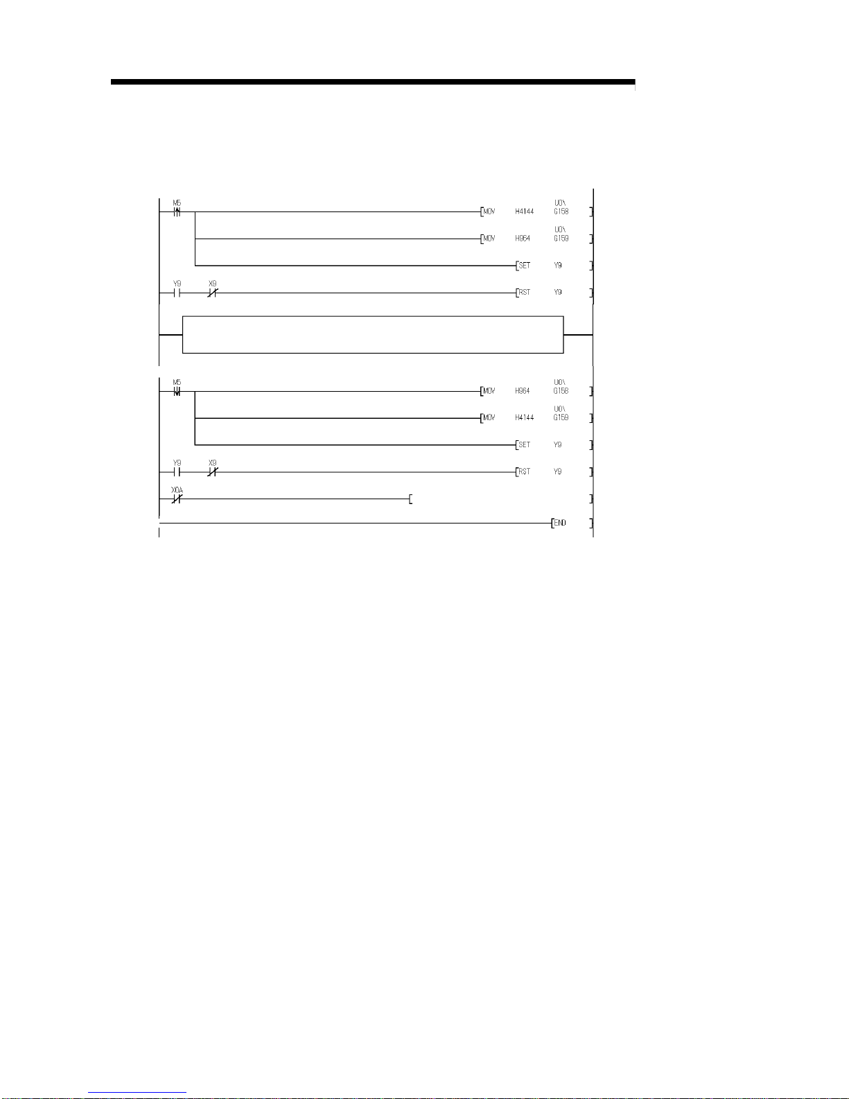
4 - 13 4 - 13
MELSEC-Q
4 SETUP AND PROCEDURES BEFORE OPERATION
(b) When switching the mode using the setting of the mode switching setting
(buffer memory addresses 158, 159: Un\G158, Un\G159) and operation
condition setting request (Y9)
Switches to offset/gain setting mode
Common program
Switches to normal mode
Processing in normal mode
Sets 4144
H
to buffer memory
address 158.
Sets 964
H
to buffer memory
address 159.
Turns ON operation condition
setting request (Y9).
Turns OFF operation condition
setting request (Y9)
Sets 964
H
to buffer memory
address 158.
Sets 4144H to buffer memory
address 159.
Turns ON operation condition
setting request (Y9).
Turns OFF operation condition
setting request (Y9).
(c) When switching the mode by making intelligent function module switch
setting
Only the common program is necessary.
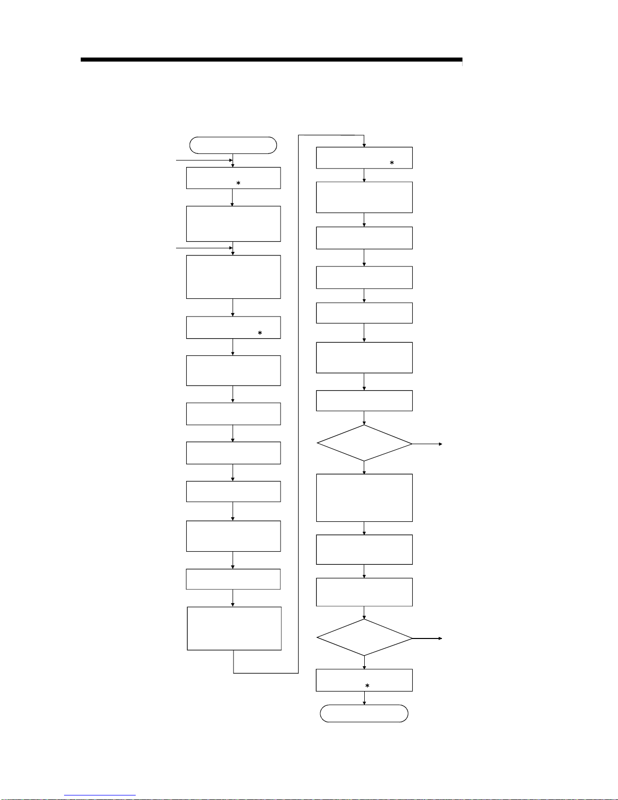
4 - 14 4 - 14
MELSEC-Q
4 SETUP AND PROCEDURES BEFORE OPERATION
4.6.2 Offset/Gain Settings (Q62AD-DGH)
(1) Offset/gain setting procedure
Switch to the normal
setting mode.
1
Start
Switch to the offset/gain
setting mode.
Verify that the mode is set
to offset/gain setting and
the RUN LED is flashing.
Set the offset setting
channel in buffer memory
address 22 (Un\G22).
Set buffer memory
address 23 (Un\G23) to 0.
Turn the channel change
request (YB) to ON.
Verify that the channel
change completed flag
(XB) is ON.
Adjust other
channels?
YES
NO
Set the channel change
request (YB) to OFF.
After verifying that the offset/
gain setting mode sta tus f lag
(XA) is OFF, turn YA OFF.
Verify that the offset/gain
setting mode status flag
(XA) is ON.
Add the current that will be
the offset value.
Set the gain setting channel
in buffer memory address
23 (Un\G23). Set buffer
memory address 22
(Un\G22) to 0.
ERR. LED lit?
YES
NO
End
Verify that the channel
change completed flag
(XB) is ON.
2)
1)
2)
1)
1
Set the offset/gain setting
request (YA) to ON and
perform th e offset/gain
settings.
Register to the Q62AD-DGH.
Add the current that
will be the gain value.
2
Turn ON the offset/gain
change request (YC).
Make sure that the offset/
gain change completed
flag (XC) is ON.
Turn OFF the offset/gain
change request (YC).
Turn ON the offset/gain
change request (YC).
Make sure that the offset/
gain change completed
flag (XC) is ON.
Turn OFF the offset/gain
change request (YC).
Turn the channel change
request (YB) to ON.
2
Set the channel change
request (YB) to OFF.

4 - 15 4 - 15
MELSEC-Q
4 SETUP AND PROCEDURES BEFORE OPERATION
1 The mode switching (normal mode to offset/gain setting mode to normal mode) method
is given below.
• Dedicated instruction (G.OFFGAN) ............. Refer to Section 4.6.2 (2), (a)
• Setting made to mode switching setting (buffer memory addresses 158, 159:
Un\G158, Un\G159) and turning the operation condition setting request (Y9) from OFF
to ON ............................................................Refer to Section 4.6.2 (2), (b)
• Intelligent function module switch setting ....Refer to Section 4.5, Section 4.6.2 (2), (c)
(After intelligent function module switch setting, reset the PLC CPU or switch power
OFF, then ON.)
2 Turning ON the channel change request (YB) starts power supply from the
corresponding channel to the 2-wire transmitter. After fully checking the wiring, settings,
etc., turn ON the ch an nel ch ang e req ue st (YB) .
POINT
(1) Perform the offset/gain settings in the range that satisfies the conditions
specified in POINT of Section 3.1.2 (2).
When the setting exceed s thi s range, the maximum re sol ution or total accur acy
may not be withi n the range i ndi cat ed in th e pe r forman ce spe ci fi cation .
(2) Though the offset/gain settings can be performed on multiple channels at the
same time, set the offset and gain separately (0 at either of the buffer memory
addresses 22, 23).
If channels are set at the buffer memory addresses 22 (Un\G22) and 23
(Un\G23) at the same time, an error will occur and the ERR. LED will be lit.
(3) After the offset/gain settings are completed, verify that the offset and gain
values have been set correctly under actual usage conditions.
(4) The offset and ga in val ue s ar e sto re d into th e E
2
PROM and are not erased at
power-off.
(5) At the time of offset/gain setting, turn ON the user range write request (YA) to
write the val ue s to the E
2
PROM.
Data can be written to the E
2
PROM up to 100 thousand ti mes.
To prevent accidental write to the E
2
PROM, an error will occur and the error
code (buffer memory address 19: Un\G19) will be stored if write is performed
26 consecutive times.
(6) If an error (error code: 40
1
) occurs during offset/gain setting, re-set the
correct offset/gain value.
The offset/gain value of the channel where the error has occurred is not written
to the A/D converter module. (
1:
indicates the co rr esp on di ng chan nel
number.)
(7) When the offset/gain setting mode is switched to the normal mode, the module
ready (X0) turns from OFF to ON.
Note that the initial setting processing will be executed at this time if there is a
sequence program that performs initial settings when the module ready (X0)
turns ON.
(8) When one mode is switched to the other (the normal mode is switched to the
offset/gain setting mode or the offset/gain setting mode is switched to the
normal mode), A/D conversion is suspended and power supply to the 2-wire
transmitter is turned OFF.
To resume A/D conversion and power supply to the 2-wire transmitter, turn ON
the operating condition setting request (Y9) after the mode is switched to the
normal mode.
(9) Buffer memory addresses 202 to 225 (Un\G202 to Un\G225) are the areas
used to restore the user range settings offset/gain values when online module
change is made.
Refer to chapter 7 for details of online module change.
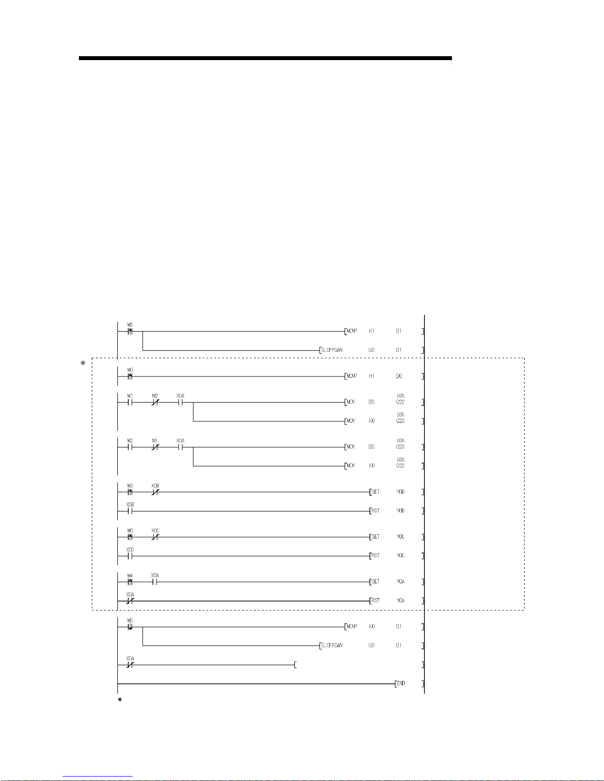
4 - 16 4 - 16
MELSEC-Q
4 SETUP AND PROCEDURES BEFORE OPERATION
(2) Program examples
The program in the dotted area of (a) is common to (a), (b) and (c).
In this example, the I/O signals for the Q62AD-DGH are X/Y0 to X/YF.
• Channel selection.....................................................................................M0
• Offset setting.............................................................................................M1
• Gain setting...............................................................................................M2
• Channel change command ......................................................................M3
• Offset/gain setting value write command to the module.........................M4
• Mode switching.........................................................................................M5
• Offset/gain change command ..................................................................M6
• Normal mode checking signal..................................................................M50
• Channel designation storage device........................................................D0
• Dedicated instruction (G.OFFGAN) setting storage device....................D1
(a) When switching the mode using the dedicated instruction (G.OFFGAN)
The following program switches to the offset/gain setting mode with the
dedicated instruction (G.OFFGAN), changes the channel where offset/gain
setting will be made, writes the offset/gain values to the Q62AD-DGH, and
then switches to the normal mode.
1
Switches to offset/gain setting mode
Specifies channel where offset/ gai n settin g will be made
Specifies channel where offset setting will be made
Specifies channel where gain setting will be made
Changes channel where offset/gain setting will be made
Registers offset/gain setting results to module
Switches to normal mode
1 The program in the dotted area is a common program.
Processing in normal mode
Stores setting of dedicated
instruction (G.OFFGAN) into D1.
Stores channel where offset/
gain setting will be made into D0.
Specifies offset setting channel.
Sets 0 to buffer memory
address 23.
Specifies gain setting channel.
Sets 0 to buffer memory
address 22.
Turns ON channel change
request (YB).
Turns OFF channel change
request (YB).
Turns ON user range change
request (YA).
Turns OFF user range change
request (YA).
Stores setting of dedicated
instruction (G.OFFGAN) into D1.
Dedicated instruction (G.OFFGAN)
Dedicated instruction (G.OFFGAN)
Changes offset/gain values
Turns ON offset/gain
change request (YC).
Turns OFF offset/gain
change request (YC).

4 - 17 4 - 17
MELSEC-Q
4 SETUP AND PROCEDURES BEFORE OPERATION
(b) When switching the mode using the setting of the mode switching setting
(buffer memory addresses 158, 159: Un\G158, Un\G159) and operation
condition setting request (Y9)
*2
A/D conversion enable/disable
setting
Switches to offset/gain setting mode
Common program
Switches to normal mode
Sets 4144
H
to buffer memory
address 158.
Sets 964
H
to buffer memory
address 159.
Turns ON operation condition
setting request (Y9).
Sets 964
H
to buffer memory
address 158.
Sets 4144
H
to buffer memory
address 159.
Turns ON operation condition
setting request (Y9).
Turns OFF operation condition
setting request (Y9).
1-second timer
Turns ON operation condition
setting request (Y9).
POINT
When switching the mode using the setting of the mode switching setting and
operation condition setting request, change the initial setting program for the
program marked
2.
(c) When switching the mode by making intelligent function module switch setting
Only the common program is necessary.
4.6.3 A/D conversion value storage during offset/gain setti ng
If during the offset/gain setting, the A/D conversion values are stored into the buffer
memory addresses 11 to 14, 54 to 61 (Un\G11 to Un\G14, Un\G54 to Un\G61) as in
the normal mode.
(1) Q64AD-GH
The A/D conversion values of all channels are stored into the buffer memory.
(2) Q62AD-DGH
The A/D conversion values of the channels specified in the offset/gain setting
mode (buffer memory addresses 22, 23: Un\G22, Un\G23) are stored into the
buffer memory.

5 - 1 5 - 1
MELSEC-Q
5 UTILITY PACKAGE (GX Configurator- AD )
5 UTILITY PACKAGE (GX Configurator-AD)
5.1 Utility Package Functions
Table 5.1 shows an overview of the utility package functions.
Table 5.1 Utility package (GX Configurator-AD) function list
Item Description Reference section
Initial setting
1
(1) Sets the following items that require initial setting.
• A/D conversion enable/disable setting
• Averaging process specification
• Average time/Average number of times/Move average/
Time constant settings
• A/D conversion starting time setting (Q62AD-DGH)
• Warning output settings (Process alarm setting)
• Process alarm upper upper limit value/upper lower limit value/
lower upper limit value/lower lower limit value
• Warning output settings (Rate alarm setting)
• Rate alarm upper limit value/lower limit value
• Rate alarm warning detection period
• Input signal error detection setting
• Input signal error detection setting value
(2) The data for which initial setting has been completed is registered in
the parameters for the PLC CPU, and automatically written to the
A/D converter module when the PLC CPU changes to the RUN
status.
Section 5.4
Automatic refresh
setting
1
(1) Sets automatic refresh for the A/D converter module buffer memory.
(2) The buffer memory that was set for automatic refresh is
automatically read and written to the specified device w hen the
END command for the PLC CPU is executed.
Section 5.5
Monitor/Test
(1) Monitor/Test
The buffer memory and I/O signals for the A/D converter modules
are monitored and tested.
(2) Operating condition setting
Changes the A/D operating status during operation.
(3) Offset/gain setting
When setting the offset/gain to a value selected by the user (when
the analog output range setting is user range setting), the offset and
gain can be easily set while viewing the screen.
(4) Pass data
The pass data (industrial shipment settings offset/gain values, u s er
range settings offset/gain values) can be monitored and set.
Section 5.6
FB conversion
Generates FB automatically from the intelligent function module
parameter (initial setting/auto refresh setting).
Section 5.7
POINT
1 If initial setting and automatic refresh setting are performed, the intelligent
function module parameters require a maximum of 76 bytes per module.
5

5 - 2 5 - 2
MELSEC-Q
5 UTILITY PACKAGE (GX Configurator- AD )
5.2 Installing and Uninstalling the Utility Package
See "Method of installing the MELSOFT Series" attached with the utility package
regarding the install and uninstall operation for the utility package.
5.2.1 User precautions
The following provides the precautions on using the GX Configurator-AD:
(1) Important safety information
Since GX Configurator-AD is add-in software for GX Developer, read "Safety
Precautions" and the basic operati ng procedu res in GX Developer's ope rating
manual.
(2) About installation
The GX Configurator-AD is an add-in package for GX Developer Version 4 or
later products. Therefore, install GX Configurator-AD in a personal computer in
which GX Developer Version 4 or a later product has been installed.
(3) About display-screen errors while usi ng the i ntelligent function
module utility
There may be cases in which the screen will not properly display while the
intelligent function module utility is being used, due to a lack of system resources.
If this occurs, close the intelligent function module utility first and then GX
Developer (program, comments, etc.) and other applications. Next, restart GX
Developer and the intelligent function module utility.
(4) To start the intelligent function module utility
(a) In GX Developer, select "QCPU (Q mode)" for the PLC series and specify
the project.
If something other than "QC PU (Q mode )" is selected for the PLC seri es, or if
the project is not specified, t he intell igent fun ction module utility will no t start.
(b) Multiple intelligent function module utilities can be started.
However, the [Open parameter]/[Save parameter] intelligent function
module's parameter operations can only be performed by a single intelligent
function module utility. Other intelligent function module utilities can perform
the [Monitor/test] operation only.
(5) How to switch screens when two or more intell ig ent function
module utilities are started
When two or more intelligent function module utility screens cannot be displayed
side by side, use the task bar to change the intelligent function module utility
screen so that it is displayed on top of other screens.
5
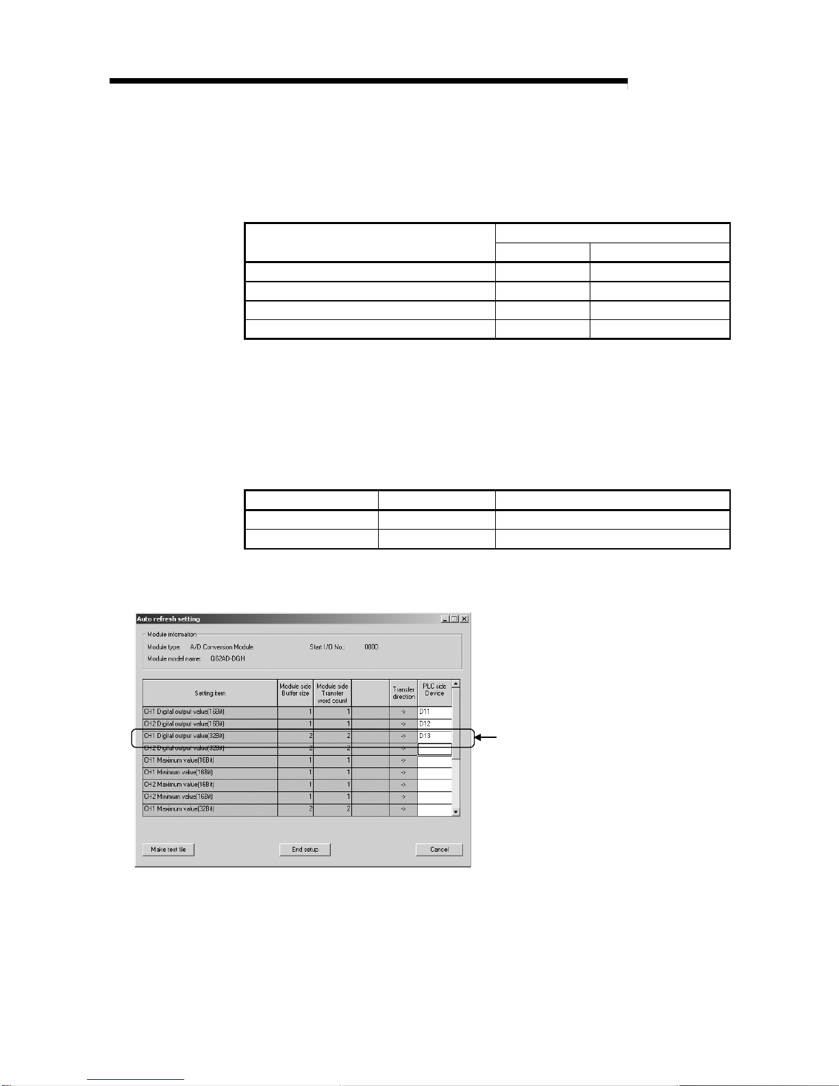
5 - 3 5 - 3
MELSEC-Q
5 UTILITY PACKAGE (GX Configurator- AD )
(6) About the number of parameters that can be set i n GX
Configurator-AD
The number of parameters that can be set by the GX Configurator for an
intelligent function module installed in the CPU module and in a remote I/O
station of the MELSECNET/H network system is limited.
Maximum number of parameter settings
Intelligent function module installation object
Initial setting Automatic refresh setting
Q00J/Q00/Q01CPU 512 256
Q02/Q02H/Q06H/Q12H/Q25HCPU 512 256
Q12PH/Q25PHCPU 512 256
MELSECNET/H remote I/O station 512 256
For example, if multiple intelligent function modules are installed in a remote I/O
station, set the GX Configurator so that the number of parameter settings of all
the intelligent function modules does not exceed the maximum number of
parameter settings. The total number of parameter settings is calculated
separately for the initial setting and for the automatic refresh setting.
The number of parameter settings that can be set for one module in the GX
Configurator-AD is as shown below.
Object Module Initial setting Automatic refresh setting
Q64AD-GH 4 (Fixed) 27 (Maximum number of settings)
Q62AD-DGH 8 (Fixed) 15 (Maximum number of settings)
Example) Counting the number of parameter settings in the automatic refresh
setting
The number of settings in this one line is counted
as one setting.
The number of settings is not counted by columns.
Add up all the setting items in this setting screen,
then add them to the total for the other intelligent
function modules to get a grand total.

5 - 4 5 - 4
MELSEC-Q
5 UTILITY PACKAGE (GX Configurator-AD)
5.2.2 Operating environment
The operating environment of the personal computer where the GX Configurator-AD is
used is explained.
Item Peripheral devices
Installation (Add-in) destination
1
Add-in to GX Developer Version 4 (English version) or later
2
Computer main unit Personal computer on which Windows® operates.
CPU
Required memory
Refer to the following table "Used operating system and performance required for
personal computer".
For installation 65 MB or more
Hard disk
free space
For operation 20 MB or more
Display 800 600 dot or more resolution
Operating system
Microsoft
®
Windows® 95 Operating System (English version)
Microsoft
®
Windows® 98 Operating System (English version)
Microsoft
®
Windows® Millennium Edition Operating System (English version)
Microsoft® Windows NT® Workstation Operating System Version 4.0 (English version)
Microsoft® Windows® 2000 Professional Operating System (English version)
Microsoft
®
Windows® XP Professional Operating System (English version)
Microsoft® Windows® XP Home Edition Operating System (English version)
1: Install the GX Configurator-AD in GX Developer Version 4 or higher in the same language.
GX Developer (English version) and GX Configurator-AD (Japanese version) cannot be used in
combination, and GX Developer (Japanese version) and GX Configurator-AD (English version) cannot be
used in configuration.
2: GX Configurator-AD cannot be used as an add-in with GX Developer Version 3 or earlier versions.
In addition, GX Developer Version 8 or later is necessary to use the FB conversion function.
Used operating system and performance required for personal computer
Performance Required for Personal Computer
Operating system
CPU Required memory
Windows® 95 Pentium® 133MHz or more 32MB or more
Windows® 98 Pentium® 133MHz or more 32MB or more
Windows® Me Pentium® 150MHz or more 32MB or more
Windows NT® Workstation 4.0 Pentium® 133MHz or more 32MB or more
Windows® 2000 Professional Pentium® 133MHz or more 64MB or more
WindowsRXP Professional (Service Pack 1 or more) PentiumR300MHz or more 128MB or more
WindowsRXP Home Edition (Service Pack 1 or more) PentiumR300MHz or more 128MB or more
POINT
New functions of WindowsRXP
When Microsoft
R
WindowsRXP Professional Operating System or
Microsoft
R
WindowsRXP Home Edition Operating System is used, the following
new functions cannot be used.
If any of the following new functions is used, this product may not operate normally.
Start of application in Windows
R
compatible mode
Fast user switching
Remote desktop
Large fonts (Details setting of Display properties)

5 - 5 5 - 5
MELSEC-Q
5 UTILITY PACKAGE (GX Configurator- AD )
5.3 Explanation of Utility Package Operation
5.3.1 How to perform common utility package operations
(1) Available control keys
Special keys that can be used during operation of the utility package and their
application s ar e show n in th e ta ble bel ow .
Name of key Application
Esc
Cancels a newly entered value when entering data in a cell.
Closes the window.
Tab
Moves between controls in the window.
Ctrl
Used in conjunction with the mouse when multiple cell s are
selected in the selection test.
Delete
Deletes the character where the cursor is positioned.
When a cell is selected, clears all of the setting contents.
Back
Space
Deletes the character where the cursor is positioned.
Moves the cursor.
Page
Up
Moves the cursor one page up.
Page
Down
Moves the cursor one page down.
Enter
Confirms the value entered in the cell.

5 - 6 5 - 6
MELSEC-Q
5 UTILITY PACKAGE (GX Configurator- AD )
(2) Data to be created with the utility package
The data and files shown below that are created with the utility package are also
processed using GX Developer operation. Figure 5.1 shows which operation
processes which data or file.
<Intelligent function module parameters>
(a) This data is created with the automatic refresh setting, and stored in the
intelligent function module parameter file of the project to be created using
GX Developer.
Project
Program
Parameter
PLC Parameter
Network Parameter
Intelligent Function Module Parameter
(b) Steps 1) to 3) shown in Figure 5.1 are performed using the following
operations.
1) Operating from GX Developer.
[Project]
[Open existing project] / [Save project] / [Save project as]
2) Operating from the utility parameter setting module selection screen.
[Intelligent function module parameter]
[Open parameter] / [Save
parameter]
3) Operating from GX Developer.
[Online]
[Read from PLC] / [Write to PLC] "Intelligent function
module parameters"
Or, operate from the utility parameter setting module selection screen.
[Online]
[Read from PLC] / [Write to PLC]

5 - 7 5 - 7
MELSEC-Q
5 UTILITY PACKAGE (GX Configurator- AD )
<Text file>
(a) A text file is created by performing the initial setting or automatic refresh
setting, or selecting text file creation
in the monitor/test screen. The text
files can be utiliz ed to crea t e use r do cumen ts.
QCPU
RUN.
ERR.
USER.
BAT.
BOOT.
RS-232
USB
Q25HCPU
MODE.
A
GX Developer/
GX Configurator-AD
Disk
Project Project
AA
B
Personal compute
r
A : Indicates an intelligent
function module parameter.
B : Indicates the data
saved by text file creation.
1)
2)
3)
Figure 5.1 Correlation chart for data created using the utility package
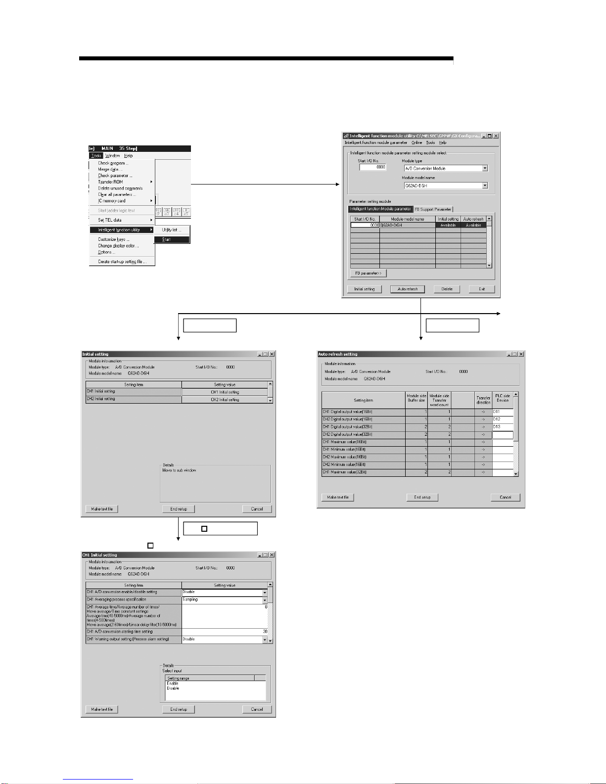
5 - 8 5 - 8
MELSEC-Q
5 UTILITY PACKAGE (GX Configurator- AD )
5.3.2 Operation overview
See Section 5.3.3
GX Developer screen
1)
setting module select screen
Initial setting scree n
Initial setting
Auto refresh
Auto refresh setting screen
See Section 5.4
See Section 5.4
See Section 5.5
[Tools] – [Intelligent function utility]– [Start]
CH Initial setting
CH Initial setting screen
Intilligent function module parameter

5 - 9 5 - 9
MELSEC-Q
5 UTILITY PACKAGE (GX Configurator- AD )
[Online] – [Monitor/test]
Select monitor/test module screen
Monitor/test screen
See Section 5.6
Enter "Start I/O No.", then select "Module type" and "Module model name".
1)
<<FB support parameter>> tab –
FB conversion screen
FB conversion
See Section 5.7
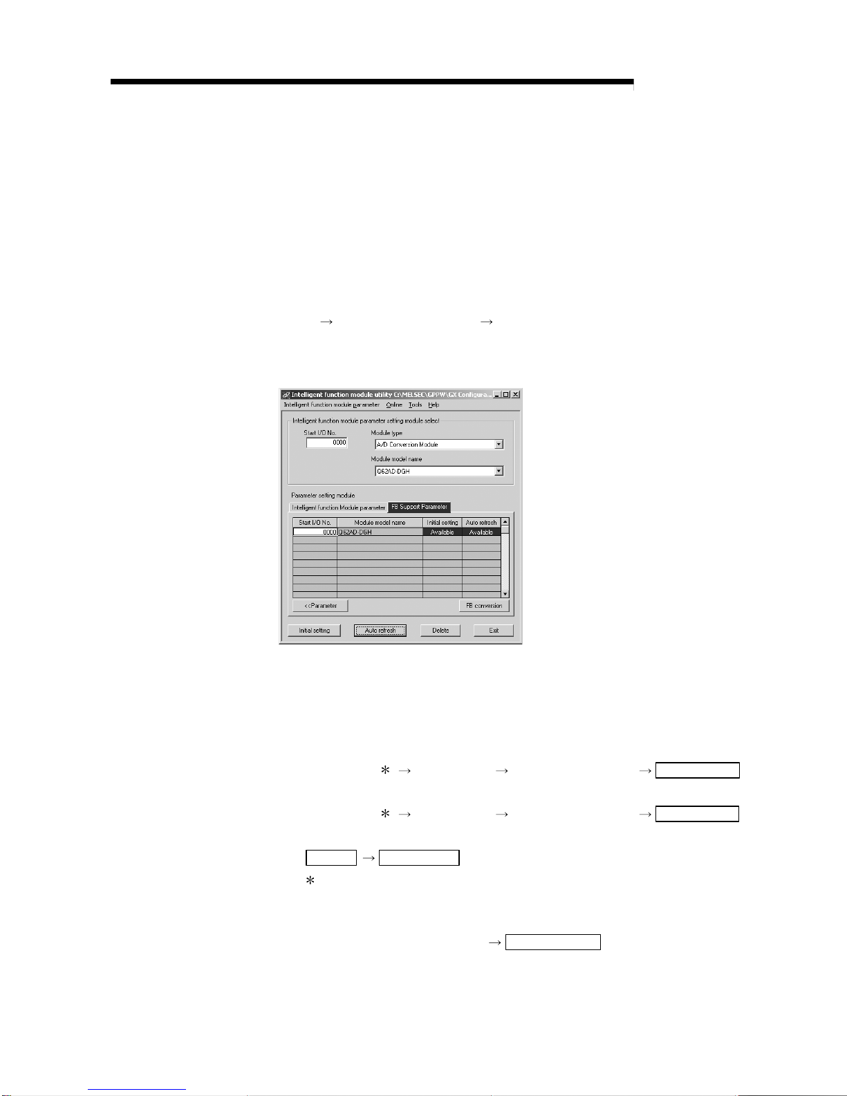
5 - 10 5 - 10
MELSEC-Q
5 UTILITY PACKAGE (GX Configurator- AD )
5.3.3 Starting the intelligent function module utility
[Purpose of setting]
Start the intelligent function module utility from GX Developer, and display the
module selection screen for the intelligent function module utility parameter
setting. The screens for performing initial setting, automatic refresh setting and
monitor/test module selection (selecting the module for which monitoring/testing
is to be performed) can be started from this screen.
[Startup procedure]
[Tools] [Intelligent function utility] [Start]
[Setting screen]
Display when the <<FB support parameter>> tab is selected
[Explanation of items]
(1) How to start each screen
Common operations to the <<Intelligent function module parameter>> tab and
<<FB support parameter>> tab
(a) Starting ini tia l se tt in g
"Start I/O No.
" "Module type" "Module model name" Initial setting
(b) Starting automatic refresh setting
"Start I/O No.
" "Module type" "Module model name" Auto refresh
(c) Monitor/test module sele ction scre en
Online
Monitor/test
Enter the start I/O numbers in hexadecimal.
On the <<FB support parameter>> tab
(a) Start-up of the FB conversion screen
<<FB support parameter>> tab
FB conversion

5 - 11 5 - 11
MELSEC-Q
5 UTILITY PACKAGE (GX Configurator- AD )
POINT
The <<FB support parameter>> tab is displayed when the project which is being
edited is a label project.
(2) Explanation of screen command buttons
Common operations to the <<Intelligent function module parameter>> tab and
<<FB support parameter>> tab
Delete
Deletes the initial setting and automatic refresh setting for the
selected module.
However, if initial setting and auto refresh setting have been
prepared and the cell of initial setting or auto refresh setting is
selected and executed, only the setting of the selected cell is
deleted.
Exit
Ends the Intelligent function module utility.
When the <<FB support parameter>> tab is selected
<<Parameter
Moves the setting of the selected line to the <<Intelligent
function module parameter>> tab.
When the <<Intelligent Function Module Parameter>> tab is selected
FB parameter>>
Moves the setting of the selected line to the <<FB support
parameter>> tab.
(3) Menu bar
(a) File items
With file operation, the intelligent function module parameters for the project
opened by GX Developer can be processed.
[Open parameter]: Reads the parameter file.
[Close parameter]: Closes the parameter file. If revisions were
made, a dialog box asking whether to save
the file appears.
[Save parameter]: Saves the parameter file.
[Delete para met er ]: Deletes the pa ra met e r file .
[Open FB support parameter]: Opens the FB support parameter file.
[Save as FB support parameter]: Saves the FB support parameter file.
[Exit]: Quits the intelligent function module utility.
(b) Online items
[Monitor/test]: Starts the monitor/test module selection screen.
[Read from PLC]: Reads the intelligent function module parameters from
the CPU module.
[Write to PLC]: Writes the intelligent function module parameters to
the CPU module.
 Loading...