

Mitsubishi Electric Corporation Semiconductor Group FX3ASJ-2 Datasheet

PRELIMINARY
Notice: This is not a final specification.
Some parametric limits are subject to change.
Jan.1999
FX3ASJ-3
OUTLINE DRAWING Dimensions in mm
MP-3
MITSUBISHI Pch POWER MOSFET
FX3ASJ-3
HIGH-SPEED SWITCHING USE
APPLICATION
Motor control, Lamp control, Solenoid control
DC-DC converter, etc.
6.5
2.3
2.3
0.9 max
1.0 max
2.3
1.0
0.5 ± 0.1
5.5 ± 0.2
10 max
2.3 min 1.5 ± 0.2
1
1
1
2
2
2
3
3
3
0.5 ± 0.2
0.8
5.0 ± 0.2
A
GATE
DRAIN
SOURCE
DRAIN
4
4
4
–150
±20
–3
–12
–3
–3
–12
30
–55 ~ +150
–55 ~ +150
0.26
VGS = 0V
VDS = 0V
L = 100µH
Typical value
Drain-source voltage
Gate-source voltage
Drain current
Drain current (Pulsed)
Avalanche drain current (Pulsed)
Source current
Source current (Pulsed)
Maximum power dissipation
Channel temperature
Storage temperature
Weight
V
V
A
A
A
A
A
W
°C
°C
g
VDSS
VGSS
ID
IDM
IDA
IS
ISM
PD
Tch
Tstg
—
Symbol
MAXIMUM RATINGS (Tc = 25°C)
Parameter Conditions Ratings Unit
•
4V DRIVE
•
VDSS .............................................................–150V
•
rDS (ON) (MAX) .................................................. 1.2Ω
•
ID ......................................................................–3A
•
Integrated Fast Recovery Diode (TYP.) ...........80ns
PRELIMINARY
Notice: This is not a final specification.
Some parametric limits are subject to change.
Jan.1999
MITSUBISHI Pch POWER MOSFET
FX3ASJ-3
HIGH-SPEED SWITCHING USE
PERFORMANCE CURVES
0
10
20
30
40
50
0 20050 100 150
–2
–3
–10
–1
–5
–7
–10
0
–2
–3
–5
–7
–10
1
–2
–3
–5
–7
–10
1
–2
–10
2
–3 –5–7 –2
–10
3
–3 –5–7
–2
–2 –3 –5–7 –2
tw = 10µs
TC = 25°C
Single Pulse
100µs
10ms
1ms
DC
0
–2
–4
–6
–8
–10
0 –4 –8 –12 –16 –20
Tc = 25°C
Pulse Test
PD = 30W
VGS = –10V
–4V
–3V
–5V
–6V
0
–1.0
–2.0
–3.0
–4.0
–5.0
0 –2–4–6–8–10
–6V
–4V
PD = 30W
VGS = –10V
–3V
–2.5V
–5V
Tc = 25°C
Pulse Test
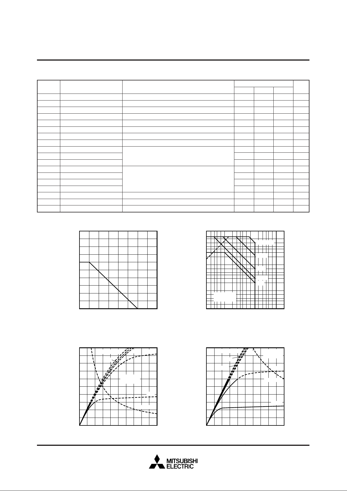
POWER DISSIPATION DERATING CURVE
CASE TEMPERATURE T
C (°C)
POWER DISSIPATION PD (W)
MAXIMUM SAFE OPERATING AREA
DRAIN-SOURCE VOLTAGE V
DS (V)
DRAIN CURRENT ID (A)
OUTPUT CHARACTERISTICS
(TYPICAL)
DRAIN CURRENT ID (A)
DRAIN-SOURCE VOLTAGE VDS (V)
OUTPUT CHARACTERISTICS
(TYPICAL)
DRAIN CURRENT ID (A)
DRAIN-SOURCE VOLTAGE VDS (V)
V
(BR) DSS
IGSS
IDSS
VGS (th)
rDS (ON)
rDS (ON)
VDS (ON)
yfs
Ciss
Coss
Crss
td (on)
tr
td (off)
tf
VSD
Rth (ch-c)
trr
V
µA
mA
V
Ω
Ω
V
S
pF
pF
pF
ns
ns
ns
ns
V
°C/W
ns
–150
—
—
–1.0
—
—
—
—
—
—
—
—
—
—
—
—
—
—
—
—
—
–1.5
0.93
1.02
–0.93
3.0
1170
81
31
9
7
82
33
–1.0
—
80
—
±0.1
–0.1
–2.0
1.20
1.32
–1.20
—
—
—
—
—
—
—
—
–1.5
4.17
—
ID = –1mA, VGS = 0V
VGS = ±20V, VDS = 0V
VDS = –150V, VGS = 0V
ID = –1mA, VDS = –10V
ID = –1A, VGS = –10V
ID = –1A, VGS = –4V
ID = –1A, VGS = –10V
ID = –1A, VDS = –5V
VDS = –10V, VGS = 0V, f = 1MHz
VDD = –80V, ID = –1A, VGS = –10V, RGEN = RGS = 50Ω
IS = –1A, VGS = 0V
Channel to case
IS = –3A, dis/dt = 100A/µs
ELECTRICAL CHARACTERISTICS (Tch = 25°C)
Drain-source breakdown voltage
Gate-source leakage current
Drain-source leakage current
Gate-source threshold voltage
Drain-source on-state resistance
Drain-source on-state resistance
Drain-source on-state voltage
Forward transfer admittance
Input capacitance
Output capacitance
Reverse transfer capacitance
Turn-on delay time
Rise time
Turn-off delay time
Fall time
Source-drain voltage
Thermal resistance
Reverse recovery time
Symbol UnitParameter Test conditions
Limits
Min. Typ. Max.
 Loading...