

Mitsubishi Electric Corporation Semiconductor Group BCR3AM Datasheet
MITSUBISHI SEMICONDUCTOR 〈TRIAC〉
BCR3AM
LOW POWER USE
NON-INSULATED TYPE, PLANAR PASSIVATION TYPE
BCR3AM
T (RMS) ........................................................................3A
•I
•V
DRM ..............................................................400V/600V
FGT !, IRGT !, IRGT # .........................30mA (15mA)
•I
✽6
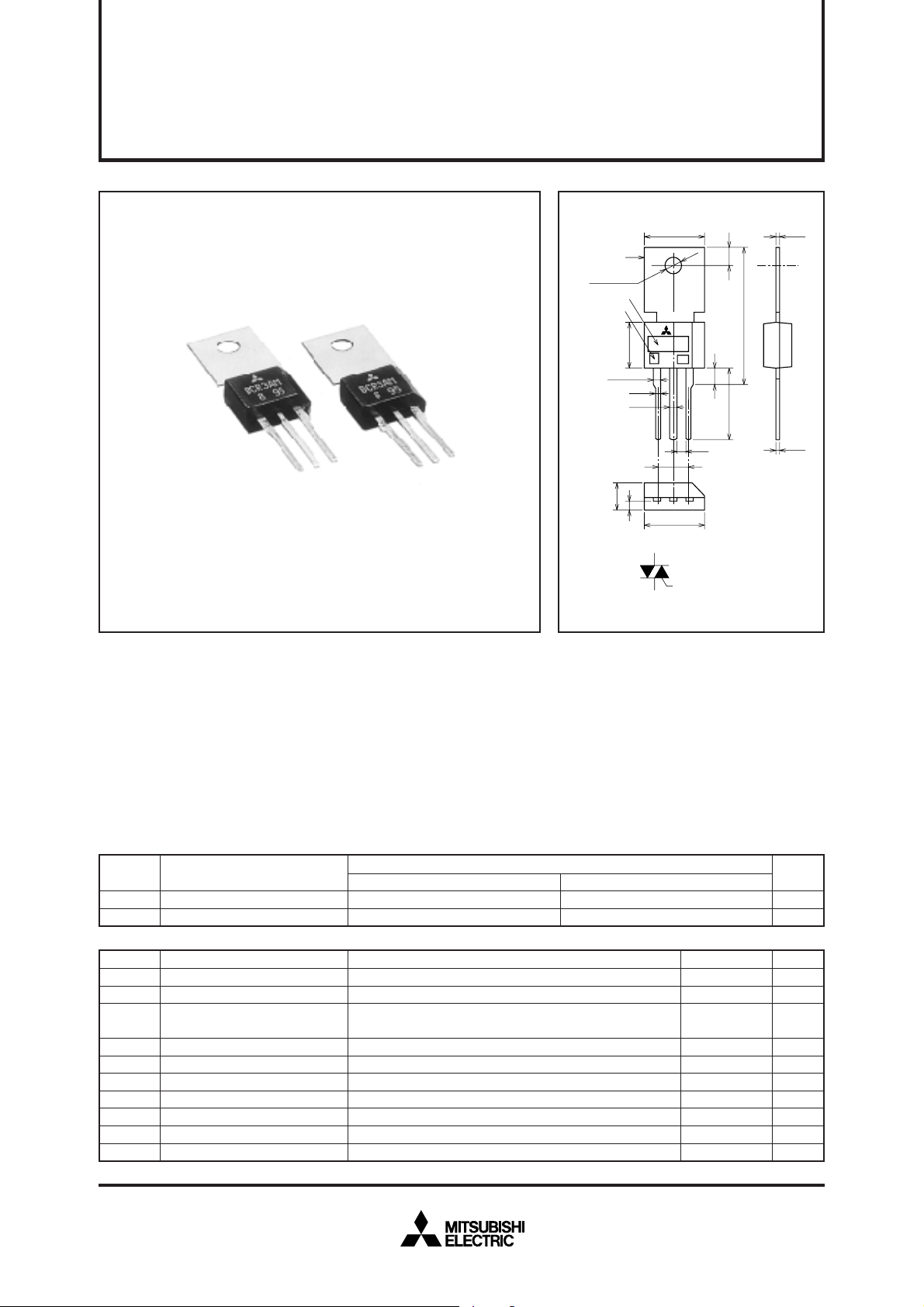
OUTLINE DRAWING
10 MAX
4
φ3.2±0.1
TYPE NAME
VOLTAGE
CLASS
1.2±0.1
4.5 MAX
8 MAX
0.8
0.8
24
1.55±0.1
1
∗
2.5 2.5
231
10 MAX
3
TO-202
1
2
3
4
Dimensions
3.2±0.2
23.7±0.5
4 MAX
12 MIN
1.5 MIN
Measurement point of
∗
case temperature
T
1
TERMINAL
T2 TERMINAL
TERMINAL
GATE
T2 TERMINAL
in mm
0.5
0.5
APPLICATION
Contactless AC switches, light dimmer, electric blankets,
control of household equipment such as electric fan,
solenoid drivers, small motor control, other general
purpose control applications
MAXIMUM RATINGS
Symbol
DRM
V
VDSM
Symbol
I
T (RMS)
ITSM
2
t
I
PGM
PG (AV)
VGM
IGM
Tj
Tstg
—
✽1. Gate open.
Repetitive peak off-state voltage
Non-repetitive peak off-state voltage
RMS on-state current
Surge on-state current
2
I
t
for fusing
Peak gate power dissipation
Average gate power dissipation
Peak gate voltage
Peak gate current
Junction temperature
Storage temperature
Weight
Parameter
Parameter
✽1
✽1
Commercial frequency, sine full wave 360° conduction, T
60Hz sinewave 1 full cycle, peak value, non-repetitive
Value corresponding to 1 cycle of half wave 60Hz, surge on-state
current
Typical value
8
400
500
Conditions
Voltage class
c=86°C
12
600
720
Ratings
3
30
3.7
3
0.3
6
0.5
–40 ~ +125
–40 ~ +125
1.6
Unit
V
V
Unit
A
A
2
A
s
W
W
V
A
°C
°C
g
Feb.1999
NON-INSULATED TYPE, PLANAR PASSIVATION TYPE
ELECTRICAL CHARACTERISTICS
Symbol
I
DRM
VTM
VFGT !
VRGT !
VRGT #
IFGT !
IRGT !
IRGT #
VGD
Rth (j-c)
(dv/dt)c
✽2.Measurement using the gate trigger characteristics measurement circuit.
✽3.The critical-rate of rise of the off-state commutating voltage is shown in the table below.
✽4.Case temperature is measured at the T
✽5.The contact thermal resistance R
✽6.High sensitivity (I
Repetitive peak off-state current
On-state voltage
Gate trigger voltage
Gate trigger current
Gate non-trigger voltage
Thermal resistance
Critical-rate of rise of off-state
commutating voltage
Parameter
T
j=125°C, VDRM applied
c=25°C, ITM=4.5A, Instantaneous measurement
T
✽2
✽2
GT≤15mA) is also available. (IGT item 1)
th (c-f) in case of greasing is 3°C/W.
!
@
j=25°C, VD=6V, RL=6Ω, RG=330Ω
T
#
!
@
j=25°C, VD=6V, RL=6Ω, RG=330Ω
T
#
j=125°C, VD=1/2VDRM
T
Junction to case
2 terminal 1.5mm away from the molded case.
Test conditions
✽4 ✽5
MITSUBISHI SEMICONDUCTOR 〈TRIAC〉
BCR3AM
LOW POWER USE
Min.
—
—
—
—
—
—
—
—
0.2
—
✽3
Limits
Typ.
—
—
—
—
—
—
—
—
—
—
—
Max.
2.0
1.5
1.5
1.5
1.5
Unit
mA
V
V
V
V
✽6
30
mA
✽6
30
mA
✽6
30
mA
—
10
—
V
°C/W
V/µs
Voltage
class
8
12
V
DRM
(V)
400
600
Min.
5
PERFORMANCE CURVES
MAXIMUM ON-STATE CHARACTERISTICS
2
10
7
TC = 25°C
5
3
2
1
10
7
5
3
2
0
10
7
5
ON-STATE CURRENT (A)
3
2
–1
10
(dv/dt) c
Unit
V/µs
Test conditions
1. Junction temperature
T
j=125°C
2. Rate of decay of on-state commutating current
c=–1.5A/ms
(di/dt)
3. Peak off-state voltage
D=400V
V
RATED SURGE ON-STATE CURRENT
40
35
30
25
20
15
10
5
SURGE ON-STATE CURRENT (A)
3.80.6 1.0 1.4 1.8 2.2 2.6 3.0 3.4
0
10023 5710123 5710
Commutating voltage and current waveforms
SUPPLY
VOLTAGE TIME
MAIN CURRENT
MAIN
VOLTAGE
44
(dv/dt)c
(inductive load)
(di/dt)c
2
TIME
TIME
V
D
ON-STATE VOLTAGE (V)
CONDUCTION TIME
(CYCLES AT 60Hz)
Feb.1999
 Loading...