

Mitsubishi Electric Corporation Semiconductor Group BCR30AM Datasheet
MITSUBISHI SEMICONDUCTOR 〈TRIAC〉
BCR30AM
MEDIUM POWER USE
NON-INSULATED TYPE, PLANAR PASSIVATION TYPE
BCR30AM
T (RMS) ......................................................................30A
•I
•V
DRM ..............................................................400V/600V
FGT !, IRGT !, IRGT # ...........................................50mA
•I
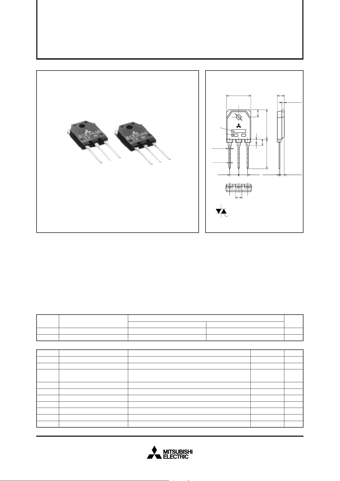
OUTLINE DRAWING
15.9 MAX
4
TYPE
NAME
VOLTAGE
CLASS
2±0.3
1.0±0.2
24
1
3
5.45
1
2
3
4
231
5.45
4
T
T
GATE
T
φ3.2±0.2
1
TERMINAL
2
TERMINAL
TERMINAL
2
TERMINAL
TO-3P
Dimensions
4.5±0.3
5.0
20.0±0.5
2
4
19.5 MIN
0.6±0.2
Measurement point of
∗
case temperature
in mm
1.5±0.2
∗
2.8±0.3
APPLICATION
Contactless AC switches, light dimmer,
on/off and speed control of small induction motors, on/off control of copier lamps,
microwave ovens
MAXIMUM RATINGS
Symbol
DRM
V
VDSM
Symbol
I
T (RMS)
ITSM
2
t
I
PGM
PG (AV)
VGM
IGM
Tj
Tstg
—
✽1. Gate open.
Parameter
Repetitive peak off-state voltage
Non-repetitive peak off-state voltage
Parameter
RMS on-state current
Surge on-state current
2
I
t
for fusing
Peak gate power dissipation
Average gate power dissipation
Peak gate voltage
Peak gate current
Junction temperature
Storage temperature
Weight
✽1
8
✽1
Commercial frequency, sine full wave 360° conduction, T
60Hz sinewave 1 full cycle, peak value, non-repetitive
Value corresponding to 1 cycle of half wave 60Hz, surge on-state
current
Typical value
400
500
Voltage class
600
720
Conditions
c=75°C
12
Ratings
30
300
378
5
0.5
10
2
–40 ~ +125
–40 ~ +125
4.8
Unit
V
V
Unit
A
A
A
W
W
V
A
°C
°C
g
2
s
Feb.1999
NON-INSULATED TYPE, PLANAR PASSIVATION TYPE
SUPPLY
VOLTAGE TIME
TIME
TIME
MAIN CURRENT
MAIN
VOLTAGE
(di/dt)c
V
D
(dv/dt)c
ELECTRICAL CHARACTERISTICS
Symbol
DRM
I
VTM
VFGT !
VRGT !
VRGT #
IFGT !
IRGT !
IRGT #
VGD
Rth (j-c)
(dv/dt)c
✽2.Measurement using the gate trigger characteristics measurement circuit.
✽3.The critical-rate of rise of the off-state commutating voltage is shown in the table below.
✽4.The contact thermal resistance R
Repetitive peak off-state current
On-state voltage
Gate trigger voltage
Gate trigger current
Gate non-trigger voltage
Thermal resistance
Critical-rate of rise of off-state
commutating voltage
Parameter
✽2
✽2
th (b-f) in case of greasing is 0.3°C/W.
!
@
#
!
@
#
j=125°C, VDRM applied
T
T
c=25°C, ITM=45A, Instantaneous measurement
T
j=25°C, VD=6V, RL=6Ω, RG=330Ω
j=25°C, VD=6V, RL=6Ω, RG=330Ω
T
j=125°C, VD=1/2VDRM
T
Junction to case
Test conditions
✽4
MITSUBISHI SEMICONDUCTOR 〈TRIAC〉
BCR30AM
MEDIUM POWER USE
Min.
—
—
—
—
—
—
—
—
0.2
—
✽3
Limits
Typ.
—
—
—
—
—
—
—
—
—
—
—
Max.
3.0
1.6
2.5
2.5
2.5
1.2
Unit
mA
V
V
V
V
50
mA
50
mA
50
mA
—
—
V
°C/W
V/µs
Voltage
class
8
12
V
DRM
(V)
400
600
(dv/dt) c
Symbol
R
L
R
L
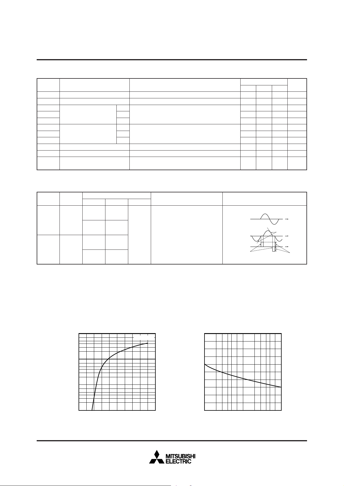
PERFORMANCE CURVES
MAXIMUM ON-STATE CHARACTERISTICS
3
10
7
5
3
2
2
10
7
5
3
2
1
10
7
5
ON-STATE CURRENT (A)
3
2
0
10
Min.
—
20
—
20
Unit
V/µs
TC = 25°C
Test conditions
1. Junction temperature
T
j=125°C
2. Rate of decay of on-state commutating current
(di/dt)
c=–16A/ms
3. Peak off-state voltage
V
D=400V
RATED SURGE ON-STATE CURRENT
500
400
300
200
100
SURGE ON-STATE CURRENT (A)
4.42.40.80.4 1.2 1.6 2.0 2.8 3.2 3.6 4.0
0
10023 5710
Commutating voltage and current waveforms
44
(inductive load)
1
23 5710
2
ON-STATE VOLTAGE (V)
CONDUCTION TIME
(CYCLES AT 60Hz)
Feb.1999
 Loading...