

Mitsubishi Electric Corporation Semiconductor Group BCR1AM-12 Datasheet
BCR1AM-12
TYPE
NAME
VOLTAGE
CLASS
2
1
3
1
2
3
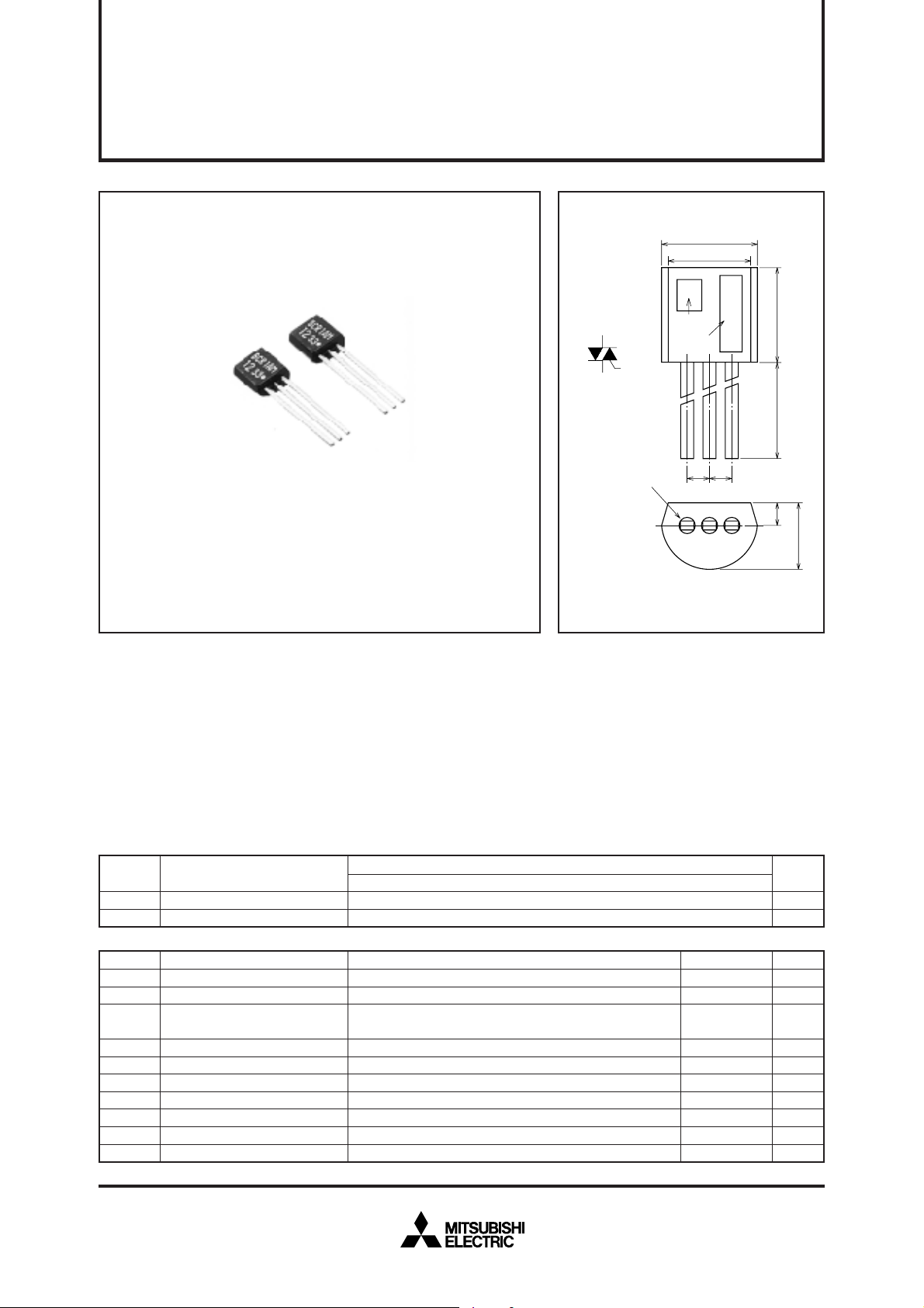
T
1
TERMINAL
T
2
TERMINAL
GATE TERMINAL
φ5.0 MAX
4.4
5.0 MAX
12.5 MIN
3.9 MAX
1.3
1.25 1.25
CIRCUMSCRIBE
CIRCLE
φ0.7
1
3
2
OUTLINE DRAWING
Dimensions
in mm
JEDEC : TO-92
MITSUBISHI SEMICONDUCTOR 〈TRIAC〉
BCR1AM-12
LOW POWER USE
GLASS PASSIVATION TYPE
•IT (RMS) ........................................................................1A
DRM .......................................................................600V
•V
•I
FGT !, IRGT !, IRGT # .............................................5mA
FGT # .....................................................................10mA
•I
APPLICATION
Contactless AC switches, heating, refrigerator, washing machine, electric fan, vending machines,
trigger circuit for low and medium triac, solid state relay,
other general purpose control applications
MAXIMUM RATINGS
✽1. Gate open.
Symbol
DRM
V
VDSM
Symbol
I
T (RMS)
ITSM
2
t
I
PGM
PG (AV)
VGM
IGM
Tj
Tstg
—
Parameter
Repetitive peak off-state voltage
Non-repetitive peak off-state voltage
Parameter
RMS on-state current
Surge on-state current
2
I
t
Peak gate power dissipation
Average gate power dissipation
Peak gate voltage
Peak gate current
Junction temperature
Storage temperature
Weight
for fusing
Voltage class
✽1
✽1
Conditions
Commercial frequency, sine full wave 360° conduction, T
60Hz sinewave 1 full cycle, peak value, non-repetitive
Value corresponding to 1 cycle of half wave 60Hz, surge on-state
current
Typical value
12
600
720
c=56°C
✽4
Ratings
1.0
10
0.41
1
0.1
6
1
–40 ~ +125
–40 ~ +125
0.23
Unit
V
V
Unit
A
A
2
A
s
W
W
V
A
°C
°C
g
Feb.1999
ELECTRICAL CHARACTERISTICS
SUPPLY
VOLTAGE TIME
TIME
TIME
MAIN CURRENT
MAIN
VOLTAGE
(di/dt)c
V
D
(dv/dt)c
Symbol
DRM
I
VTM
VFGT !
VRGT !
VRGT #
VFGT #
IFGT !
IRGT !
IRGT #
IFGT #
VGD
Rth (j-c)
(dv/dt)c
✽2.Measurement using the gate trigger characteristics measurement circuit.
✽3.The critical-rate of rise of the off-state commutating voltage is shown in the table below.
✽4.Case temperature is measured at the T
Repetitive peak off-state current
On-state voltage
Gate trigger voltage
Gate trigger current
Gate non-trigger voltage
Thermal resistance
Critical-rate of rise of off-state
commutating voltage
Parameter
✽2
✽2
j=125°C, VDRM applied
T
T
c=25°C, ITM=1.5A, Instantaneous measurement
!
@
T
j=25°C, VD=6V, RL=6Ω, RG=330Ω
#
$
!
@
T
j=25°C, VD=6V, RL=6Ω, RG=330Ω
#
$
T
j=125°C, VD=1/2VDRM
Junction to case
2 terminal 1.5mm away from the molded case.
Test conditions
✽4
MITSUBISHI SEMICONDUCTOR 〈TRIAC〉
BCR1AM-12
LOW POWER USE
GLASS PASSIVATION TYPE
Min.
—
—
—
—
—
—
—
—
—
—
0.1
—
✽3
Limits
Typ.
—
—
—
—
—
—
—
—
—
—
—
—
—
Max.
1.0
1.6
2.0
2.0
2.0
2.0
Unit
mA
V
V
V
V
V
5
mA
5
mA
5
mA
10
mA
—
50
—
V
°C/W
V/µs
Voltage
class
12
V
DRM
(V)
600
(dv/dt) c
Min.
2
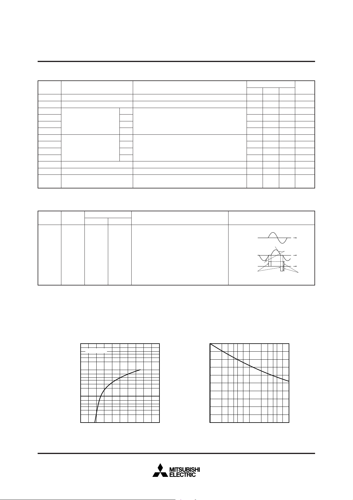
PERFORMANCE CURVES
MAXIMUM ON-STATE CHARACTERISTICS
2
10
7
TC = 25°C
5
3
2
1
10
7
5
3
2
0
10
7
5
ON-STATE CURRENT (A)
3
2
–1
10
Unit
1. Junction temperature
T
j=125°C
2. Rate of decay of on-state commutating current
V/µs
(di/dt)
c=–0.5A/ms
3. Peak off-state voltage
V
D=400V
Test conditions
4.42.40.80.4 1.2 1.6 2.0 2.8 3.2 3.6 4.0
Commutating voltage and current waveforms
(inductive load)
RATED SURGE ON-STATE CURRENT
10
8
6
4
2
SURGE ON-STATE CURRENT (A)
0
10023 5710
44
1
23 5710
2
ON-STATE VOLTAGE (V)
CONDUCTION TIME
(CYCLES AT 60Hz)
Feb.1999
 Loading...