Mitsubishi Electric Corporation Semiconductor Group BCR08AS-8 Datasheet

MITSUBISHI SEMICONDUCTOR 〈TRIAC〉
BCR08AS-8
LOW POWER USE
NON-INSULATED TYPE, PLANAR PASSIVATION TYPE
BCR08AS-8
•IT (RMS) .....................................................................0.8A
DRM .......................................................................400V
•V
•I
FGT !, IRGT !, IRGT # .............................................5mA
FGT # .....................................................................10mA
•I
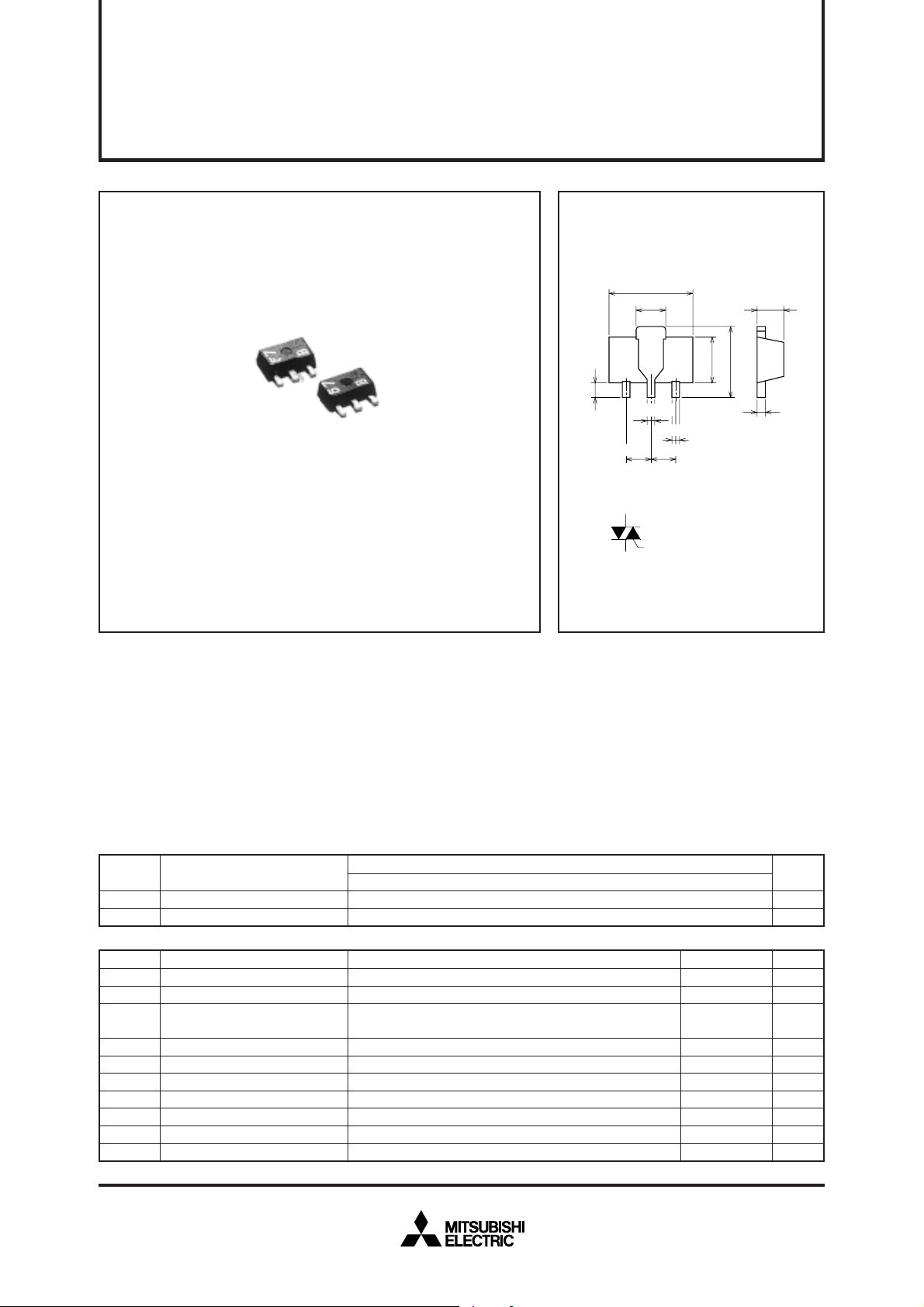
OUTLINE DRAWING
4.4±0.1
1.6±0.2
2
1
0.8 MIN
1.5±0.11.5±0.1
(Back side)
2
1
3
0.5±0.07
0.4±0.07
3
SOT-89
Dimensions
1.5±0.1
2.5±0.1
3.9±0.3
+0.03
0.4
–0.05
T
1
TERMINAL
1
2
TERMINAL
T
2
GATE TERMINAL
3
in mm
APPLICATION
Hybrid IC, solid state relay,
control of household equipment such as electric fan · washing machine,
other general purpose control applications
MAXIMUM RATINGS
Symbol
DRM
V
VDSM
Symbol
I
T (RMS)
ITSM
2
t
I
PGM
PG (AV)
VGM
IGM
Tj
Tstg
—
✽1. Gate open.
Parameter
Repetitive peak off-state voltage
Non-repetitive peak off-state voltage
Parameter
RMS on-state current
Surge on-state current
2
I
t
for fusing
Peak gate power dissipation
Average gate power dissipation
Peak gate voltage
Peak gate current
Junction temperature
Storage temperature
Weight
✽1
✽1
Commercial frequency, sine full wave 360° conduction, T
60Hz sinewave 1 full cycle, peak value, non-repetitive
Value corresponding to 1 cycle of half wave 60Hz, surge on-state
current
Typical value
Voltage class
8 (marked “B•”)
400
500
Conditions
a=40°C
Unit
V
V
✽4
Ratings
0.8
8
0.26
1
0.1
6
1
–40 ~ +125
–40 ~ +125
48
Unit
A
A
A
W
W
V
A
°C
°C
mg
2
s
Feb.1999

NON-INSULATED TYPE, PLANAR PASSIVATION TYPE
SUPPLY
VOLTAGE TIME
TIME
TIME
MAIN CURRENT
MAIN
VOLTAGE
(di/dt)c
V
D
(dv/dt)c
ELECTRICAL CHARACTERISTICS
Symbol
DRM
I
VTM
VFGT !
VRGT !
VRGT #
VFGT #
IFGT !
IRGT !
IRGT #
IFGT #
VGD
Rth (j-a)
(dv/dt)c
✽2.Measurement using the gate trigger characteristics measurement circuit.
✽3.The critical-rate of rise of the off-state commutating voltage is shown in the table below.
✽4.Mounted on 25mm × 25mm × t0.7mm ceramic plate with solder.
Repetitive peak off-state current
On-state voltage
Gate trigger voltage
Gate trigger current
Gate non-trigger voltage
Thermal resistance
Critical-rate of rise of off-state
commutating voltage
Parameter
✽2
✽2
j=125°C, VDRM applied
T
T
c=25°C, ITM=1.2A, Instantaneous measurement
!
@
T
j=25°C, VD=6V, RL=6Ω, RG=330Ω
#
$
!
@
T
j=25°C, VD=6V, RL=6Ω, RG=330Ω
#
$
T
j=125°C, VD=1/2VDRM
Junction to case
Test conditions
✽4
MITSUBISHI SEMICONDUCTOR 〈TRIAC〉
BCR08AS-8
LOW POWER USE
Min.
—
—
—
—
—
—
—
—
—
—
0.1
—
✽3
Limits
Typ.
—
—
—
—
—
—
—
—
—
—
—
—
—
Max.
1.0
2.0
2.0
2.0
2.0
2.0
Unit
mA
V
V
V
V
V
5
mA
5
mA
5
mA
10
mA
—
65
—
V
°C/W
V/µs
Voltage
class
8
V
DRM
(V)
400
(dv/dt) c
Min.
2
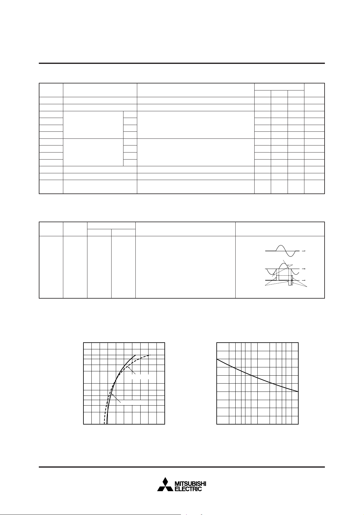
PERFORMANCE CURVES
MAXIMUM ON-STATE CHARACTERISTICS
1
10
7
5
4
3
2
0
10
7
5
4
3
ON-STATE CURRENT (A)
2
–1
10
012
Unit
1. Junction temperature
T
j=125°C
2. Rate of decay of on-state commutating current
V/µs
(di/dt)
c=–0.4A/ms
3. Peak off-state voltage
V
D=400V
Test conditions
Tj = 125°C
Tj = 25°C
345
Commutating voltage and current waveforms
(inductive load)
RATED SURGE ON-STATE CURRENT
10
8
6
4
2
SURGE ON-STATE CURRENT (A)
0
10023 5710
44
1
23 5710
2
ON-STATE VOLTAGE (V)
CONDUCTION TIME
(CYCLES AT 60Hz)
Feb.1999
 Loading...