Page 1

APPLICATION NOTE
Silicon RF Power Semiconductors
Document NO. AN-GEN-042-D
Date : 14
Rev. date : 22
Rev.date : 7
Prepared : Y.Tanaka
Confirmed : T.Okawa
(Taking charge of Silicon RF by
MIYOSHI Electronics)
th
Dec. 2007
th
Jun. 2010
th
Jan. 2010
SUBJECT: RECOMMENDATION of THERMAL COMPOUND APPLYING
METHOD for RA series RoHS COMPLIANCE PRODUCTS
GENERAL:
In order to keep high reliability of the equipment, it is better to keep the module
temperature low. The case temperature of the module is recommended to keep lower
than 90 deg. C under all conditions, and to keep lower than 60 deg. C under standard
conditions.
Therefore, when the module is mounted onto a heat sink of equipment, thermal
compound to get heat sinking should be applied between the module’s fin and the heat
sink. Following thermal compound is recommended. “G746 Shinetsu Chemical
Industry Co., Ltd.” or equivalent.
This Application note shows the applying method of thermal compound to MITSUBISHI
RA series RoHS compliance products.
Please note, this method is only general recommendation. Each user can apply
thermal compound by using each applying method as equivalent as ours.
1. Apply the Suitable Amount of Thermal Compound.
Apply thermal compound to the backside of module flange or mounted area of module on the
chassis. Control the amount of compound for each module package size by using “screen
mask” or alternative. (see following table)
Package type Flange size
(mm)
H46S 30 x 7.4 15
H11S 60.5 x 11 100
H2S 66 x 17 120
H2M 66 x 17 70
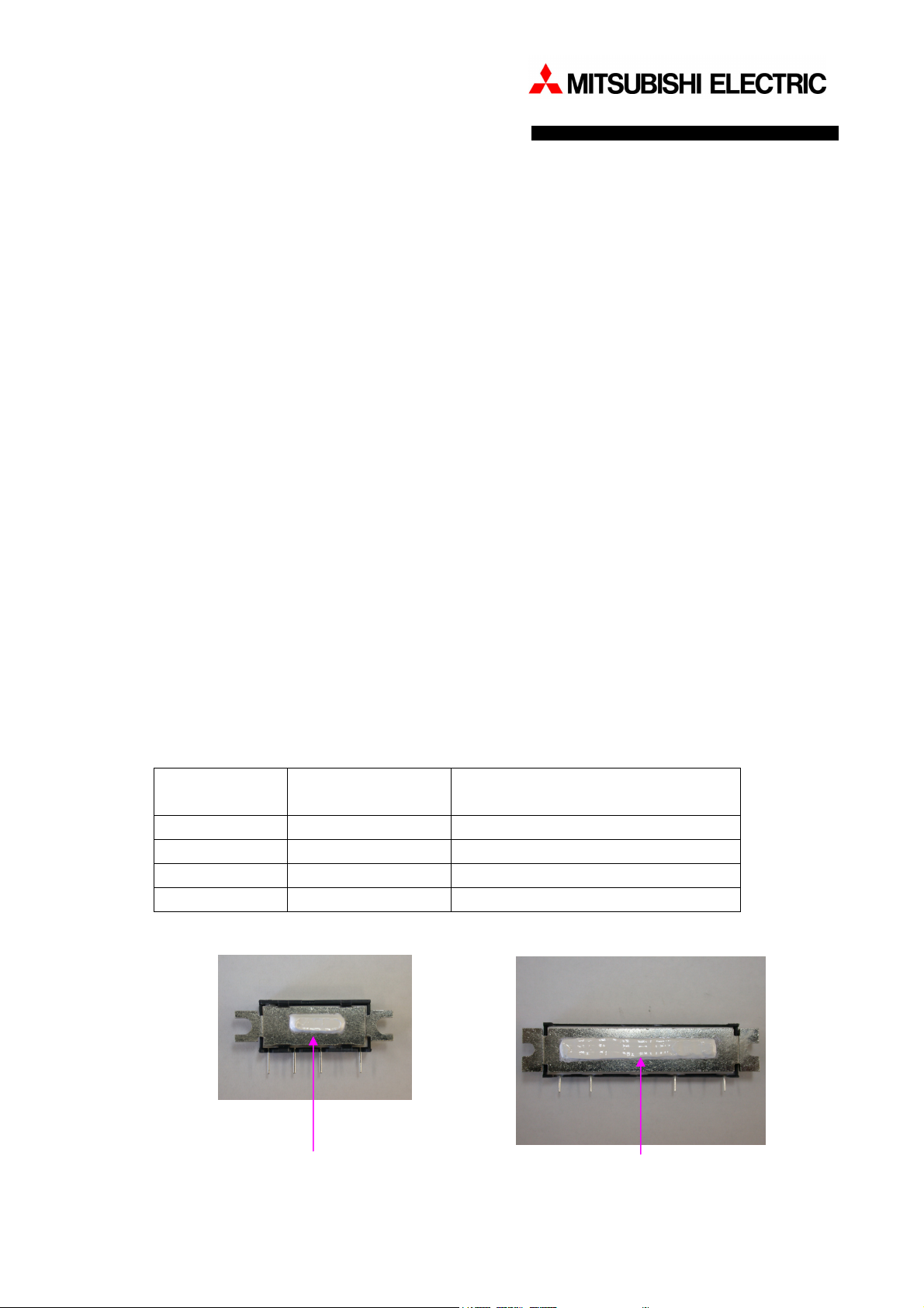
Examples of applying thermal compound
H46S package
Thermal compound size:
L10 x W3.0 x t 0.5mm
Minimum amount of compound
3
)
(mm
H11S package
Thermal compound size:
L40 x W5.0 x t 0.5mm
Application Note for Silicon RF Power Semiconductors
1/2
Page 2

Recommendation of Thermal Compound Applying Method for RA series
- AN-GEN-042-D-
H2S package
Thermal compound size:
L40 x W6.0 x t 0.5mm
H2M package
Thermal compound size:
L35 x W4.0 x t 0.5mm
2. Tighten the Screw Alternately.
Mounting the modules should be given careful instruction and their procedures monitored at
regular intervals. Since the flanges are punched from a roll of material, there can
sometimes be a small “roll – up” at the end of the mounting flange. If the mounting
hardware were tightened completely at one end first, it is easy to see that the other end
could be “lifted” off the mounting surface well in excess of the allowable flange bending
tolerance. And this method will also occur uneven thickness of thermal compound. This
should be avoided by first lightly alternately snubbing down the mounting hardware
“finger-tight.” Next, the hardware can be torqued to its final specification again in at least to
sequential steps.
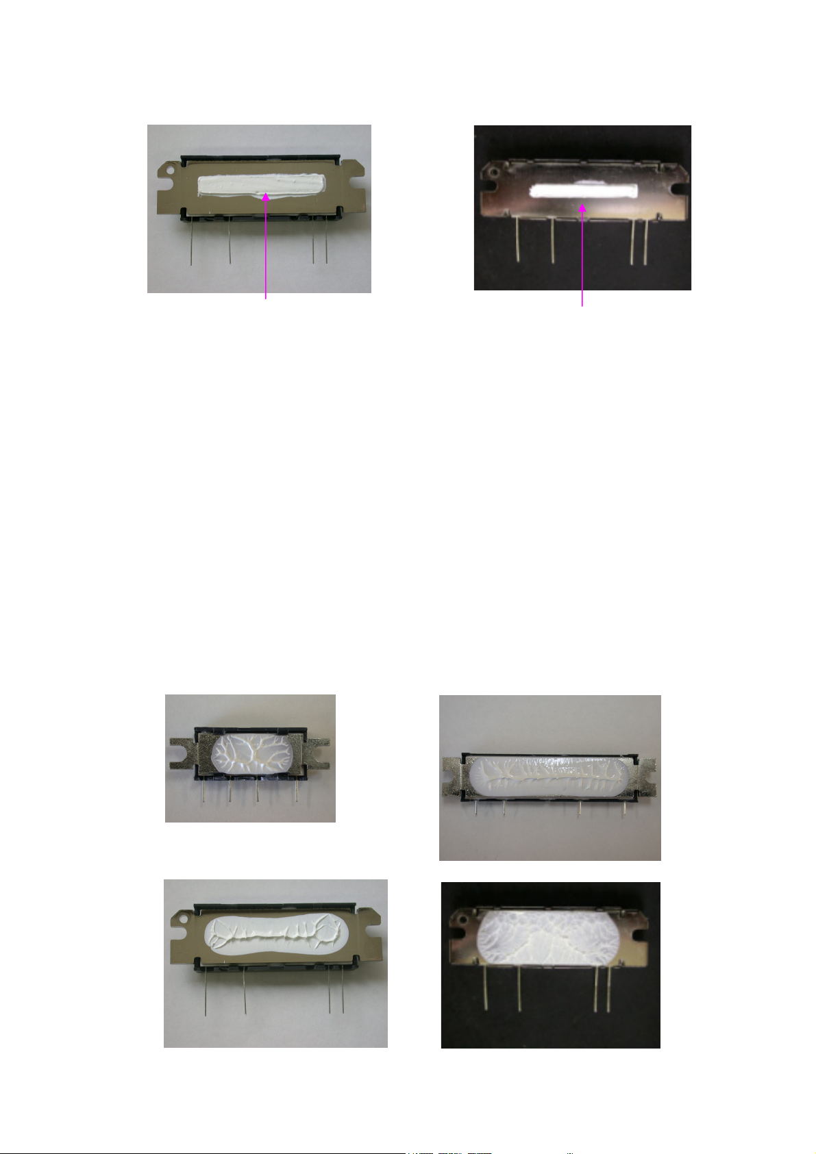
3. Keep the Pasted Area.
To get good (lower) thermal resistance between flange and chassis, pasted area of thermal
compound should be keep more than 80% of dented area on back side of the flange.
Please check the figure of thermal compound on the flange after tightened to chassis.
Examples of thermal compound figure
H46S package
H11S package
H2S package
H2M package
Application Note for Silicon RF Power Semiconductors
2/2
 Loading...