

Page 1

APPLICATION NOTE
App
Silicon RF Power Semiconductors
Document NO. AN-GEN-034-E
Date : 5
Rev. date : 22
Prepared : K.Nakamura
Confirmed : S.Kametani
(Taking charge of Silicon RF by
MIYOSHI Electronics)
SUBJECT: Recommended mounted & precaution for RD07&RD02 series with SLP package
SUMMARY:
This application note shows recommendation device mount method & precaution
for RD07&RD02 series.
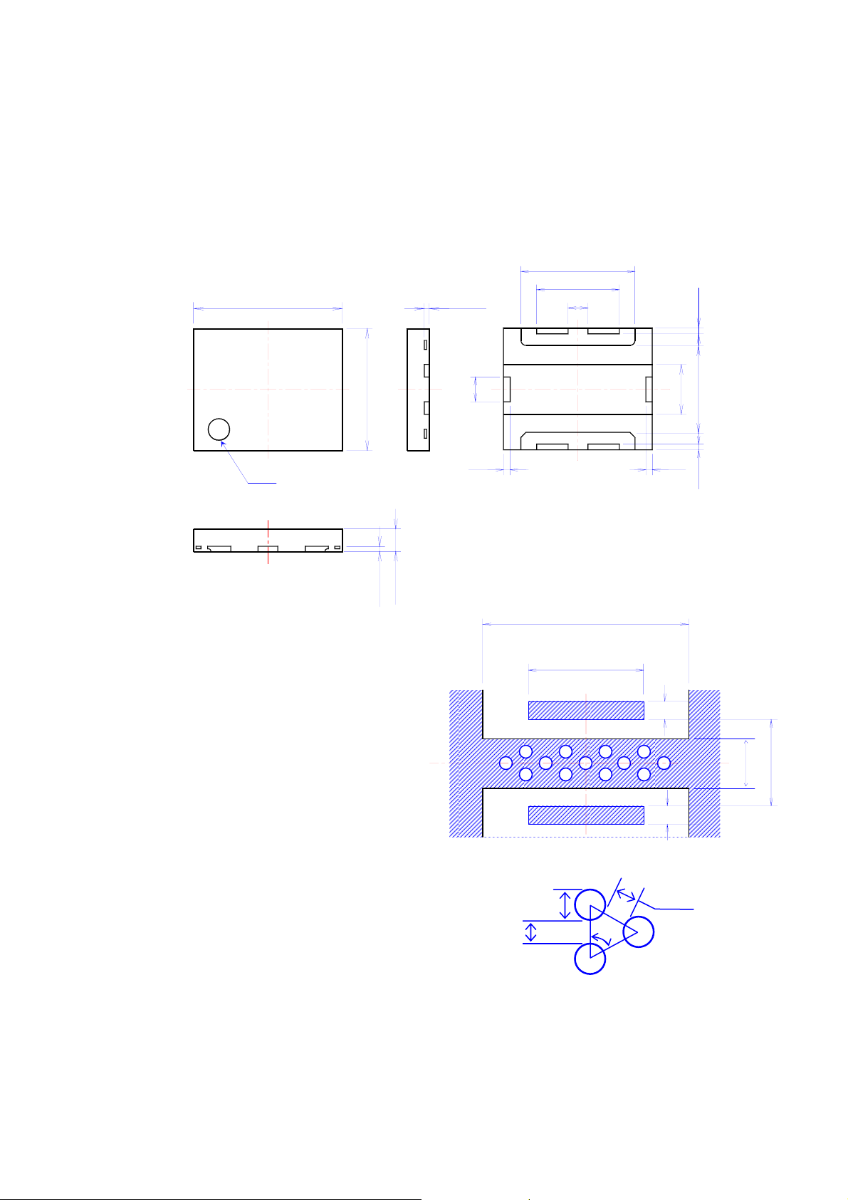
1. Recommended P.C.B layout
th
Dec. 2003
th
.Jun. 2010
2. Recommended mount method
3. Pch vs. Ta at recommend device mounting
4. Junction thermal calculation
5. Recommended reflow soldering
6. Precaution
lication Note for Silicon RF Power Semiconductors
1/7
Page 2
Recommended mounted & precaution for RD07&RD02 series with SLP package
App
0.8+/
05
8.0
AN-GEN-034-E
1. Recommended P.C.B layout (Power dissipation (Pd) capability is between
11~14W@Ta=25°C)
PACKAGE DIMENSIONS
6.0+/-0.15
0.2+/-0.05
4.6+/-0.05
3.3+/-0.05
1
-0.
(0.22)
4.9+/-0.15
1.0+/-0.05
INDEX
(0.25) (0.25)
2
2.0+/-0.05
3.5+/-0.05
3
(0.22)
RECOMMENDED P.C.B LAYOUT
0.9+/-0.1
Terminal
1.Drain
2.Source
3.Gate
0.2+/-0.05
4.7
0.8
Note
( ): center value
Unit: mm
2.0
3.4
0.8
0.5
0.4
60°
0.4
REGULAR TRIANGLE ARRANGEMENT
THROUGH HOLE
lication Note for Silicon RF Power Semiconductors
2/7
Page 3
Recommended mounted & precaution for RD07&RD02 series with SLP package
App
AN-GEN-034-E
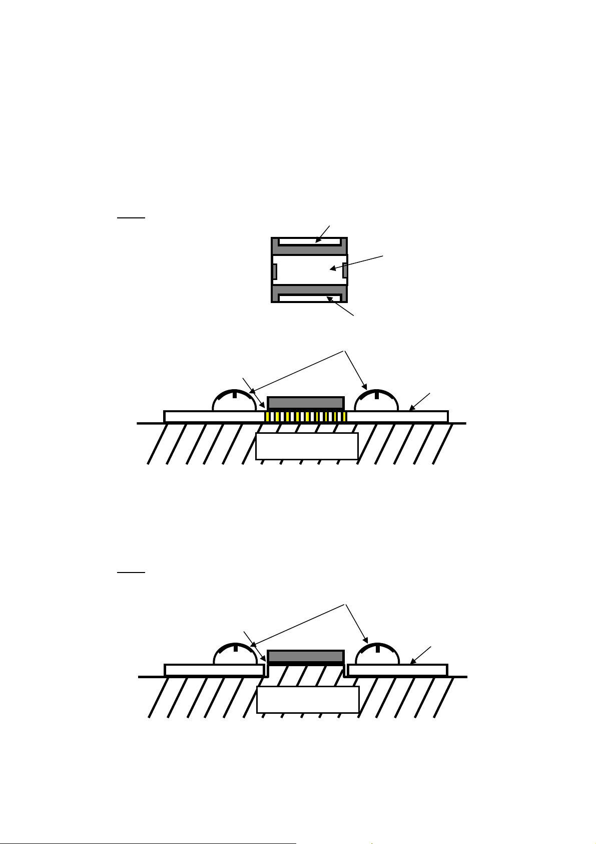
2. Recommended mount method
In order to heat radiation, Mitsubishi recommends device mount like Fig.1. And this PCB has
regular triangle arrangement 13 through holes (Page2/7) at the underside of source area. And
the plating thickness of through hole is 0.05mm. Also, fix the PCB with screws
Fig.1
Drain
Source
Gate
fix with screws.
Reflow soldering
Printed Circuit board
heat sink
# Note: Mitsubishi Heat Sink size=40.0*90.0*10.0 Unit: mm
If you need to operate more high power, Mitsubishi recommends device
mount like Fig.2. (Please fix the source of device backside directly on heatsink by solder.)
Fig.2
Reflow soldering
fix with screws.
Printed Circuit board
heat sink
lication Note for Silicon RF Power Semiconductors
3/7
Page 4
Recommended mounted & precaution for RD07&RD02 series with SLP package
App
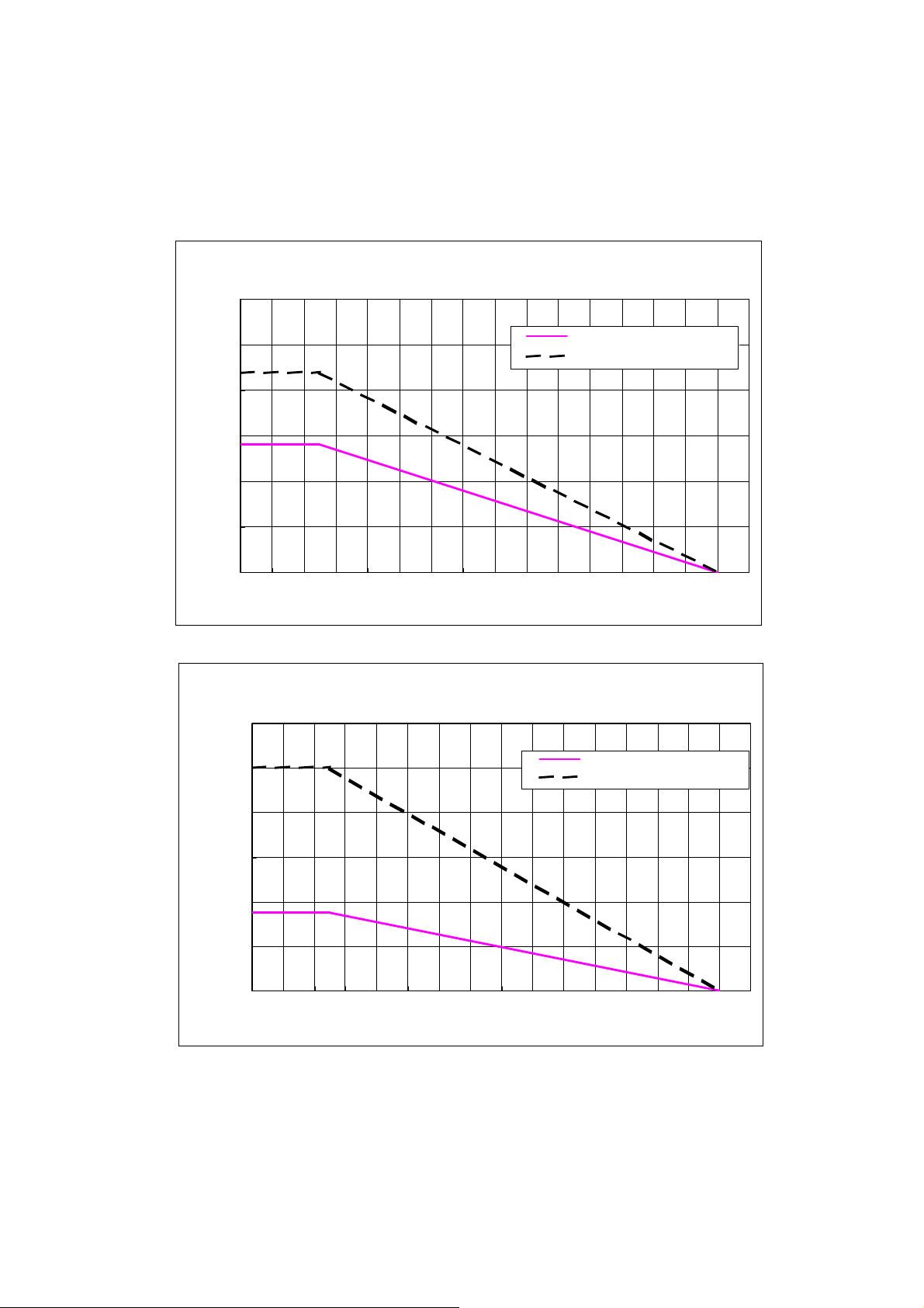
3. Pch vs Ta at recommend device mounting
Fig.3
AN-GEN-034-E
Pch(W)
Fig.4
RD02MUS1
Pch v s Ta
30
25
20
15
10
5
0
0 10 20 30 40 50 60 70 80 90 100 110 120 130 140 150 160
on PCB wit h heat sink Rthj -a= 9. 0℃/W
on heat s ink Rthj -c=5.7℃/W
on PCB w ith heat sink (Fig.1 )
on heat sink (Ta=Tc Fig.2)
Ta(℃)
RD07MVS1
on heat si nk Rthj-c=2.5℃/W
60
Pch v s Ta
on PCB with heat sink Rt hj -a= 7.2℃/W
50
40
30
Pch(W)
20
10
# Note : Mitsubishi PCB size=40.0*90.0 , t=0.8 ,material:FR4
The plating thickness of through hole=0.05
on PCB w ith heat sink (Fig.1)
on heat sink (Ta=Tc Fig.2)
0
0 10 20 30 40 50 60 70 80 90 100 110 120 130 140 150 160
Ta(℃)
Mitsubishi heat sink size=40.0*90.0*10.0 UNIT:mm
lication Note for Silicon RF Power Semiconductors
4/7
Page 5

Recommended mounted & precaution for RD07&RD02 series with SLP package
App
4. Junction thermal calculation
This example shows junction thermal calculation of RD02 and RD07 series.
RD02series
1.Thermal resistance(Rthj-a)typical value @ on PCB with regular triangle arrangement
through hole mounting heat sink.
Rthj-a=9.0 °C / W
2. Temperature of chip junction part (Tj)
In case of Ta=60 °C
Tj=78.7 °C @ Vdd=7.2V,Pin=0.05W, Po=2.0W,Idd=0.56A
AN-GEN-034-E
#Tj(°C) = Rthj-a (9.0)*Pd(2.082) +Ta(60)
Pd(W)=Vdd(7.2)*Idd(0.56)-Po(2.0)+Pin(0.05)
This value (Tj=78.7°C) is lower than 150°C of the case Absolute Maximum Ratings,
And gets to operate in the sufficiently derated condition.
RD07series
1.Thermal resistance(Rthj-a)typical value @ on PCB with regular triangle arrangement
through hole mounting heat sink.
Rthj-a=7.2 °C / W
2. Temperature of chip junction part (Tj)
In case of Ta=60 °C
Tj=115.7 °C @ Vdd=7.2V,Pin=0.7W, Po=7.0W,Idd=1.95A
# Tj(°C) = Rthj-a (7.2)*Pd(7.74)+Ta(60)
Pd(W)=Vdd(7.2)*Idd(1.95)-Po(7.0)+Pin(0.7)
This value (Tj=115.7°C) is lower than 150°C of the case Absolute Maximum Ratings,
And gets to operate in the sufficiently derated condition.
lication Note for Silicon RF Power Semiconductors
5/7
Page 6
Recommended mounted & precaution for RD07&RD02 series with SLP package
App
AN-GEN-034-E
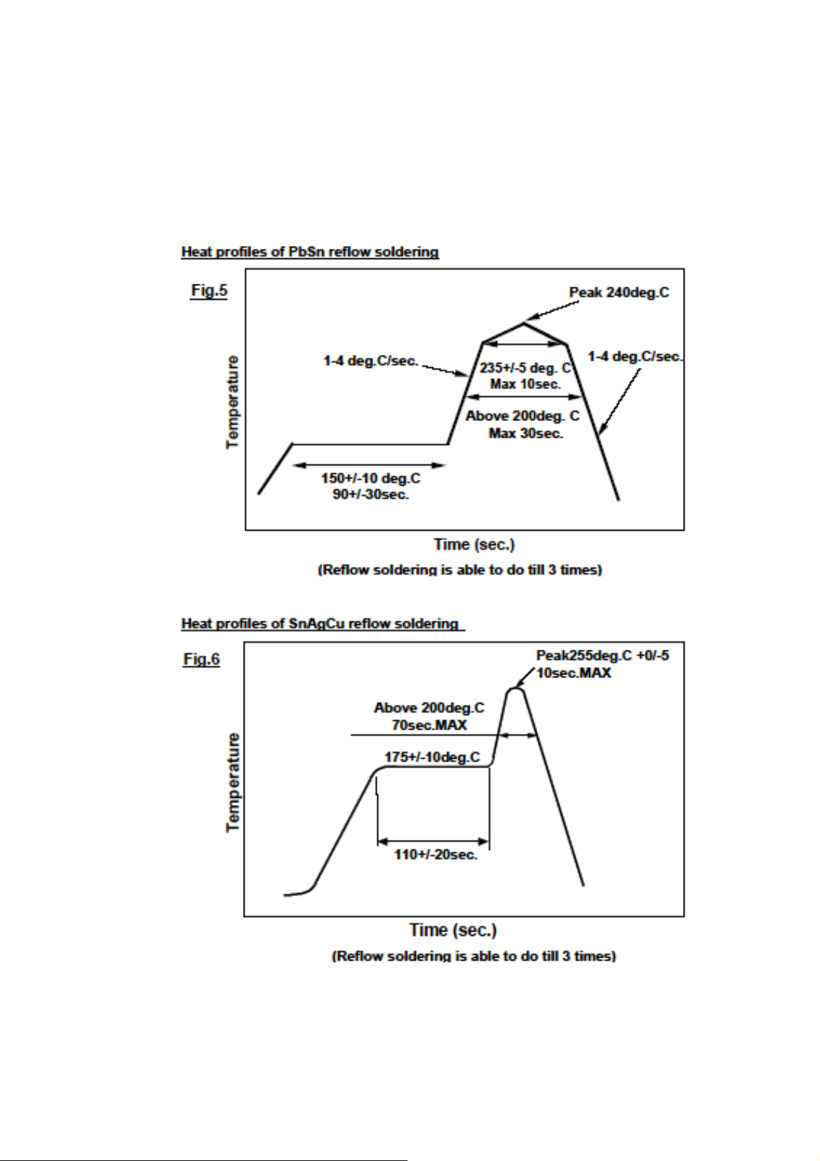
5. Recommended reflow soldering
Regarding to reflow soldering, Mitsubishi recommend the following heat profile.
lication Note for Silicon RF Power Semiconductors
6/7
Page 7

Recommended mounted & precaution for RD07&RD02 series with SLP package
App
AN-GEN-034-E
6. Precaution
GENERAL
RD**** is designed for Mobile Communication terminals. They are not designed for Base Station applications.
MITSUBISHI ELECTRIC cannot take any liability for failures resulting from Base Stations operation time or
conditions exceeding those normally found in Mobile Communication terminals. In the case of using this
devices for Base Stations or similar applications which have same operating conditions described above, the
following conditions may result in failures.
1)Junction Temperature.
Keep the operating junction temperature of MOSFETs Tch (op) less than 120deg.C.
2) Frequent on/off switching.
On/off switching causes thermal expansion of the resin covering chips and wire bonds. In Frequent and
long term Base Station usage this mechanical stress causes the wire bonds to break resulting in reduced
or no output power. Other problems can occur when applying RD**** for highly demanding Base Station
applications.
Handling precautions
1). MOS FET devices have lower surge endurance compared with silicon bipolar devices.
And there is a possibility of burn-out when static electricity or surge is added to devices.
2). These devices do not have a surge protection circuit (internal zener diode) from gate to source.
Limiting mechanical stress
1) Board Assembly : Keep mechanical stress to the devices as low as possible.
Electrical performance degradation may occur when the device is under high mechanical stress such as
board bending during reflow soldering process, board separation process, mounting to chassis, etc.
Cause of the performance degradation is delamination between molding compound and leadframe within
the device due to the transmitted mechanical stress during board bending. Please adhere to the following
guidelines in your assembly process.
2) Guideline for limiting mechanical stress to the device(Only the direction of Gate-Drain)
The curvature radius of the board shall be larger than 507mm. For example, the board warpage shall be
smaller than 2mm in case of the 90mm length board.(Fig.7) In addition to limiting the curvature radius
(2mm at 90mm length),the number of repetition for such stress should be limited to 5 times maximum.
This kind of warpage is caused both mechanically and thermally. The level of mechanical stress depends
on board materials and design layout, (location and direction of the devices), please monitor and control
curvature radius or warpage of board after re-flow process.
Curvature Radius :507mm
Curvature Radius :507mm
Warpage
(ex:2mm)
Length of the board (ex:90mm)
Fig.7
lication Note for Silicon RF Power Semiconductors
7/7
 Loading...