

Mitsubishi AJ65BT-64DAV, AJ65BT-64DAI User Manual
Digital-Analog Converter Module Type AJ65BT-64DAV/DAI
User,s Manual
Mitsubishi Programmable Controller

A - 1
• SAFETY PRECAUTIONS •
(Read these precautions before using.)
When using Mitsubishi equipment, thoroughly read this manual and the associated manuals introduced in
this manual. Also pay careful attention to safety and handle the module properly.
The precautions given in this manual are concerned with this product. Refer to the user's manual of the
CPU module to use for a description of the PLC system safety precautions.
These
SAFETY PRECAUTIONS classify the safety precautions into two categories: “DANGER” and
“CAUTION”.
DANGER
Procedures which may lead to a dangerous condition and cause death or serious
injury if not carried out properly.
CAUTION
Procedures which may lead to a dangerous condition and cause superficial to
medium injury, or physical damage only, if not carried out properly.
Depending on circumstances, procedures indicated by CAUTION may also be linked to serious
results.
In any case, it is important to follow the directions for usage.
Store this manual in a safe place so that you can take it out and read it whenever necessary. Always
forward it to the end user.
[DESIGN PRECAUTIONS]
!
DANGER
• Configure a safety circuit so that the safety of the overall system is maintained even when an
external power error or PLC error occurs.
Accident may occur due to output error or malfunctioning.
(1) The status of analog output changes depending on the setting of various functions that
control the analog output. Take sufficient caution when setting for those functions.
For details of analog output status, refer to Section 3.4.5 “Combinations of functions in each
part”
(2) Normal output may not be obtained due to malfunctions of output elements or the internal
circuits. Configure a circuit to monitor signals which may lead to a serious accident
!
CAUTION
• Do not bunch the control wires or communication cables with the main circuit or power wires, or
install them close to each other.
They should be installed 100mm(3.9inch) or more from each other.
Not doing so could result in noise that would cause erroneous operation.
• At power ON/OFF, voltage or current may instantaneously be output from the output terminal of
this module.
In such case, wait until the analog output becomes stable to start controlling the external device.
A - 2
[INSTALLATION PRECAUTIONS]
!
CAUTION
• Use the module in the environment given in the general specifications of this Manual.
Using the module outside the range of the general specifications may result in electric shock,
fire or malfunctioning, or may damage or degrade the module.
• Securely fix the module with seated P-shape pan screws to the installation holes (two locations).
Improper installation may result in breakdowns or cause the module to fall out.
• Do not touch the conducted area of the module.
Doing so may cause module malfunctioning or breakdowns.
[WIRING PRECAUTIONS]
!
CAUTION
Be sure to shut off all phases of the external power supply used by the system before installation
or wiring.
Not doing so can cause the product to be damaged or malfunction.
• Always ground the FG terminal to the protective ground conductor.
Failure to ground these terminals may cause malfunctioning.
Use applicable solderless terminals and tighten them with the specified torque. If any solderless
spade terminal is used, it may be disconnected when the terminal screw comes loose, resulting
in failure.
• When wiring the module, check the rated voltage and terminal layout of the wiring, and make
sure the wiring is done correctly. Connecting a power supply that differs from the rated voltage
or wiring it incorrectly may cause fire or breakdown.
• Tighten the terminal screws with the specified torque. If the terminal screws are loose, it may
result in short circuits, fire or malfunctioning.
• Be careful not to let foreign matter such as filings or wire chips get inside the module. These can
cause fire, breakdowns and malfunctioning.
When connecting the communication and power supply cables to the module, always run them
in conduits or clamp them.
Not doing so can damage the module and cables due to loose, moved or accidentally pulled
cables or can cause a malfunction due to a cable connection fault.
• Do not install the control lines together with the communication cables, or bring them close to
each other. Failure to do so may cause malfunctions due to noise.
When disconnecting the communication and power supply cables from the module, do not hold
and pull the cable part.
Disconnect the cables after loosening the screws in the portions connected to the module.
Pulling the cables connected to the module can damage the module and cables or can cause a
malfunction due to a cable connection fault.
A - 3
[STARTING AND MAINTENANCE PRECAUTIONS]
!
CAUTION
• Do not touch the terminals while the power is on. Doing so may cause malfunctioning.
• Be sure to shut off all phases of the external power supply used by the system before cleaning
or retightening the terminal screws.
Not doing so can cause the module to fail or malfunction.
Undertightening can cause a drop, short circuit or malfunction.
Overtightening can cause a drop, short circuit or malfunction due to damage of the screws or
module.
• Never disassemble or modify the module.
This may cause breakdowns, malfunctioning, injury and/or fire.
Do not drop the module or give it hard impact since its case is made of resin. Doing so can
damage the module.
Be sure to shut off all phases of the external power supply used by the system before mounting
or dismounting the module to or from the panel.
Not doing so can cause the module to fail or malfunction.
Do not install/remove the terminal block more than 50 times after the first use of the product.
(IEC 61131-2 compliant)
• Always make sure to touch the grounded metal to discharge the electricity charged in the body,
etc., before touching the module.
Failure to do so may cause a failure or malfunctions of the module.
[DISPOSABLE PRECAUTIONS]
!
CAUTION
• When disposing of this product, treat it as industrial waste.
A - 4
REVISIONS
* The manual number is given on the bottom left of the back cover.
Print Date * Manual Number Revision
Jan., 1997 SH(NA)-3615-A First printing
Jun., 2000 SH(NA)-3615-B Addition of Q series types
Chapter 2, Section 3.2, Section 3.4.1, Section 3.6.3, Section 4.2,
Section 6.2
Partial changes
Section 1.1(3), Section 3.1, Section 3.2, Section 3.4.5, Section 4.1,
Section 4.6.2, Section 4.7.2, Section 5.2
Sep., 2004 SH(NA)-3615-C
Addition
Conformation to the EMC Directive and Low Voltage Instruction
Correction
SAFETY PRECAUTIONS, About this Manual, Chapter 1, Chapter 2,
Section 3.1, Section 3.2, Section 3.6.4, Section 3.6.5, Section 4.1,
Section 4.4, Section 4.6, Section 4.6.1, Section 4.6.2, Section 4.7.2,
Chapter 5, Section 6.2
Jul., 2005 SH(NA)-3615-D
Correction
SAFETY PRECAUTIONS
Oct., 2006 SH(NA)-3615-E
Correction
SAFETY PRECAUTIONS, Section 4.2
Dec., 2006 SH(NA)-3615-F
Partial correction
Chapter 2(1), Section 3.5.1, Chapter 5
Japanese Manual Version SH-3600-H
This manual does not imply guarantee or implementation right for industrial ownership or implementation
of other rights. Mitsubishi Electric Corporation is not responsible for industrial ownership problems caused
by use of the contents of this manual.
© 1997 MITSUBISHI ELECTRIC CORPORATION

A - 5
Introduction
Thank you for purchasing the Mitsubishi Graphic Operation Terminal.
Before using the equipment, plese read this manual carefully to develop full familiarity with the functions and
performance of the graphic operation terminal you have purchased, so as to ensure correct use.
Please forward a copy of this manual to the end user.
Table of Contents
About This Manual
1. OVERVIEW 1- 1 to 1- 2
1.1 Features ................................................................................................................................................... 1- 1
2. SYSTEM CONFIGURATION 2- 1 to 2- 2
3. SPECIFICATIONS 3- 1 to 3-14
3.1 General Specification............................................................................................................................... 3- 1
3.2 Performance Specification....................................................................................................................... 3- 2
3.3 I/O Conversion Characteristics................................................................................................................ 3- 4
3.3.1 Offset value and gain value........................................................................................................... 3- 4
3.3.2 I/O conversion characteristics ....................................................................................................... 3- 4
3.4 Various Functions to Control the Analog Output .................................................................................... 3- 8
3.4.1 Function to specify hold or clear of the analog output when the PLC CPU is in the STOP status
(HOLD/CLEAR setting)................................................................................................................. 3- 8
3.4.2 Function to specify executing or not executing the D/A conversion processing
(Analog output enable signal) ....................................................................................................... 3- 8
3.4.3 Function to specify enabling or prohibiting of the analog value external output
(Analog output enable/prohibit setting) ........................................................................................ 3- 8
3.4.4 Offset/gain setting.......................................................................................................................... 3- 8
3.4.5 Combinations of various functions ................................................................................................ 3- 8
3.5 I/O Signals to the Master Station............................................................................................................ 3-10
3.5.1 I/O signal list ................................................................................................................................. 3-10
3.5.2 Functions of the I/O signals.......................................................................................................... 3-11
3.6 Remote Register ..................................................................................................................................... 3-12
3.6.1 Allocation of the remote register ..................................................................................................3-12
3.6.2 Digital value setting area for channels 1 through 4 ..................................................................... 3-13
3.6.3 Analog output enable/prohibit channel ........................................................................................ 3-13
3.6.4 Set value checking code storage area for channels 1 through 4 ............................................... 3-14
3.6.5 Error code..................................................................................................................................... 3-14

A - 6
4. Setup and Preparation before Operation 4- 1 to 4- 8
4.1 Precautions when Handling..................................................................................................................... 4- 1
4.2 Name of Each Part................................................................................................................................... 4- 2
4.3 Offset/Gain Setting................................................................................................................................... 4- 4
4.4 Station Number Setting............................................................................................................................ 4- 5
4.5 Facing Direction of the Module Installation ............................................................................................. 4- 5
4.6 Data Link Cable Wiring ............................................................................................................................ 4- 6
4.6.1 Precautions when handling the CC-Link dedicated cable ........................................................... 4- 6
4.6.2 CC-Link dedicated cable connections .......................................................................................... 4- 6
4.7 Wiring........................................................................................................................................................ 4- 7
4.7.1 Precautions when wiring ............................................................................................................... 4- 7
4.7.2 Wiring between the AJ65BT-64DAV/DAI and external devices .................................................. 4- 7
5. PROGRAMMING 5- 1 to 5-16
5.1 Programming Procedure.......................................................................................................................... 5- 1
5.2 Conditions of Program Example.............................................................................................................. 5- 2
5.3 Program Example for Use of the QCPU (Q mode)................................................................................. 5- 4
5.4 Program Example for Use of the QnACPU............................................................................................. 5- 9
5.5 Program Example for Use of the ACPU/QCPU (A mode) (dedicated instructions) ............................ 5- 10
5.6 Program Example for Use of the ACPU/QCPU (A mode) (FROM/TO instructions) ........................... 5- 14
6. TROUBLESHOOTING 6- 1 to 6- 2
6.1 Error Code List ......................................................................................................................................... 6- 1
6.2 Troubleshooting ....................................................................................................................................... 6- 1
6.2.1 When a communication fault occurs between the master station and this module .................... 6- 2
APPENDIX App- 1 to App- 4
Appendix 1 External Dimensions of the AJ65BT-64DAV .........................................................................App- 1
Appendix 2 External Dimensions of the AJ65BT-64DAI...........................................................................App- 2
A - 7
About this Manual
The following are manuals related to this product.
Request for the manuals as needed according to the chart below.
Related Manuals
Manual Name
Manual No.
(Type code)
CC-Link System Master/Local Module User's Manual type AJ61BT11/A1SJ61BT11
Describes the system configuration, performance specifications, functions, handling, wiring and
troubleshooting of the AJ61BT11 and A1SJ61BT11. (Optionally available)
IB-66721
(13J872)
CC-Link System Master/Local Module User's Manual type AJ61QBT11/A1SJ61QBT11
Describes the system configuration, performance specifications, functions, handling, wiring and
troubleshooting of the AJ61QBT11 and A1SJ61QBT11. (Optionally available)
IB-66722
(13J873)
CC-Link System Master/Local Module User's Manual type QJ61BT11N
Describes the system configuration, performance specifications, functions, handling, wiring and
troubleshooting of the QJ61BT11N. (Optionally available)
SH-080394E
(13JR64)
Conformation to the EMC Directive and Low Voltage Instruction
When complying with EMC Directives and Low-Voltage Directives by assembling a
Mitsubishi PLC compatible with EMC Directive and Low-Voltage Directives into the
user product, refer to Chapter 3 "EMC Directives and Low-Voltage Directives" in the
User’s Manual (Hardware) for the CPU module being used.
The CE logo is printed on the rating plate on the main body of the PLC that conforms
to the EMC directive and low voltage instruction.
To conform this product to the EMC Directive and Low Voltage Directive, refer to the
Section of "CC-Link Modules" in Chapter 3 "EMC Directive and Low Voltage
Directive" of the User's Manual (Hardware) of the CPU module used.

1. OVERVIEW MELSEC-A
1-1
1. OVERVIEW
This user's manual describes the specification and handling of AJ65BT-64DAV digital analog voltage
conversion module (abbreviated as AJ65BT-64DAV from here on) and AJ65BT-64DAI digital analog
current conversion module (abbreviated as AJ65BT-64DAI from here on), which is used as the remote
device station for the CC-Link system.
(1) AJ65BT-64DAV
This is a module which converts the digital values (16-bit encoded binary value) set in the PLC
CPU to analog values (-10V to 0V to 10V voltage), and performs an external output to four
channels.
(2) AJ65BT-64DAI
This is a module which converts the digital values (16-bit encoded binary value) set in the PLC
CPU to analog values (4mA to 20mA current), and performs an external output to four channels.
In this manual, the name which refers to both AJ65BT-64DAV and AJ65BT-64DAI is abbreviated as
“AJ65BT-64DAV/DAI.”
1.1 Features
The AJ65BT-64DAV/DAI has the following features:
(1) One module can provide four channels of D/A conversion.
The AJ65BT-64DAV/DAI can produce output of analog values (voltage/current) to four external
devices.
(2) The analog-output enable/prohibit setting is possible for each channel.
The sequence program can specify whether to enable or prohibit analog output to the external
devices after the D/A conversion for each channel.
Analog output from the channel where the analog output is prohibited will be 0V or 0mA.
(3) You can make the analog output hold/clear setting at a PLC CPU stop or link error occurrence (all
channels batch).
Using the HOLD/CLR terminal, you can select whether to hold or clear the analog output at the
instant the PLC CPU is set to a STOP status or a link error occurs.
(4) Offset and gain setting
When a fine I/O conversion characteristic is required, the offset and gain setting of each channel
can be set without a volume control, enabling to modify the I/O conversion characteristic as
desired.
1

1. OVERVIEW MELSEC-A
1-2
MEMO
1

2. SYSTEM CONFIGURATION MELSEC-A
2-1
2. SYSTEM CONFIGURATION
(1) Applicable CPU
(a) When the master module is AJ61BT11:
A0J2CPU A0J2HCPU A1CPU A2CPU(S1) A3CPU
A1NCPU A2NCPU(S1) A3NCPU A3MCPU A3HCPU
A2ACPU(S1) A3ACPU A2UCPU(S1) A3UCPU A4UCPU
A73CPU
A1SCPU(C24-R2) A1SJCPU A2SCPU A2USCPU(S1)
Q02CPU-A Q02HCPU-A Q06HCPU-A
A1SJHCPU A1SHCPU A2SHCPU
(b) When the master module is AJ61QBT11:
Q2ACPU(S1) Q3ACPU Q4ACPU
Q2ASCPU(S1) Q2ASHCPU(S1)
(c) When the master module is A1SJ61BT11:
A1SCPU(C24-R2) A1SJCPU A2SCPU A2USCPU(S1)
Q02CPU-A Q02HCPU-A Q06HCPU-A
A1SJHCPU A1SHCPU A2SHCPU
(d) When the master module is A1SJ61QBT11:
Q2ASCPU(S1) Q2ASHCPU(S1)
(e) When the master module is QJ61QBT11/QJ61BT11N:
Q00JCPU Q00CPU Q01CPU
Q02CPU Q02HCPU Q06HCPU Q12HCPU Q25HCPU
Q12PHCPU Q25PHCPU
Q12PRHCPU Q25PRHCPU
2

2. SYSTEM CONFIGURATION MELSEC-A
2-2
MEMO
2
3. SPECIFICATIONS MELSEC-A
3-1
3. SPECIFICATIONS
The general specifications, performance specifications, and I/O characteristics of the
AJ65BT-64DAV/DAI are explained.
3.1 General Specification
The general specifications of the AJ65BT-64DAV/DAI are shown in Table 3.1.
Table 3.1 General specification
Item Specification
Usage ambient
temperature
0 to 55°C
Storage ambient
temperature
-20 to 75°C
Usage ambient humidity 10 to 90%RH, no condensation
Storage ambient humidity 10 to 90%RH, no condensation
Compliancy standard JIS B 3502, IEC61131-2
Frequency Acceleration Amplitude
Sweep count
10 to 57Hz —
0.075mm
(0.0030inch)
When there is
intermittent vibration
57 to 150Hz 9.8m/s
2
—
10 times in each
direction X, Y, Z (80
minutes)
10 to 57Hz —
0.035mm
(0.0014inch)
Vibration durability
When there is
continuous vibration
57 to 150Hz 4.9m/s
2
—
—
Shock durability
Conforming to JIS B 3502, IEC61131-2
(147m/s
2
, 3 times each in XYZ directions)
Usage environment No corrosive gas
Usage height *3 Less than 2000 m (Less than 6562 ft.)
Installation area Within the control board
Over-voltage category *1 Less than II
Pollution rate *2 Less than 2
Remark
*1 Indicates the location where the device is connected from the public cable network to the device
structure wiring area.
Category II applies to the devices to which the power is supplied from a fixed equipment.
Surge withstand voltage for devices with up to 300V of rated voltage is 2500V.
*2 This is an index which indicates the degree of conductive object generation in the environment
where the device is used. Level 2 is an environment where only nonconductive objects are
formed with some chances of temporary conductivity generation due to occasional condensation.
*3 Do not operate or store the PLC in the environment where the pressure applied is equal to
greater than the atmospheric pressure at the altitude of 0m.
Doing so may cause a malfunction. Please consult our branch office when the PLC is to be
operated under pressure.
3
3. SPECIFICATIONS MELSEC-A
3-2
3.2 Performance Specification
The performance specification of the AJ65BT-64DAV/DAI is shown Table 3.2:
Table 3.2 Performance specification
Specification
Item
AJ65BT-64DAV AJ65BT-64DAI
16-bit encoded binary (valid bit: 12 bits)
Digital input value
-2048 to 2047 0 to 4095
Analog conversion value
Voltage: -10 to 10VDC
(External load resistance: 2kΩ to 1MΩ)
Current: 4 to 20mADC
(External load resistance: 0 to 600Ω)
Digital input value
Analog conversion
value
Digital input value
Analog conversion
value
+2000 +10V 4000 +20mA
+1000 +5V 2000 +12mA
0 ±0V 0 +4mA
-1000 -5V
I/O characteristics
-2000 -10V
Offset/gain adjustment Yes (user setting or factory setting)
Maximum resolution *1 5mV 4μA
Total accuracy *2
(accuracy for the maximum value)
± 1% (± 100mV) ± 1% (±200
μ
A)
Maximum conversion speed *3 Max. 1ms per channel (4ms per 4 channels)
Output short-circuit protection Yes
Insulation system
Across output channels: Non-insulated
Across external supply power and analog output: Transformer insulated
Analog output points 4 channels per module
I/O occupied points
2 stations: 32 points each for RX/RY
8 points each for RWr/RWw
Connector terminal block 27-point terminal block (M3.5 × 7 screws)
Supported cable size 0.75 to 2.00mm2
Supported solderless terminal RAV 1.25-3.5 (according to JIS C 2805), RAV 2-3.5
Module installation screw
M4 x 0.7mm x 16mm or larger screw (tightening torque 78 to 118N⋅cm)
Installable with the DIN rail.
Supported DIN rail
TH35-7.5Fe, TH35-7.5Al,TH35-15Fe
(conforming to JIS C 2812)
24V DC (20.4V DC to 26.4V DC)
Inrush current: 1.5A, within 0.67ms Inrush current: 3.2A, within 0.43ms
External supply power
Current consumption:0.18A Current consumption:0.27A
Noise resistance
Noise voltage: 500Vp-p
Measured using a noise simulator with 1μs of noise amplitude and 25 to 60Hz of noise frequency.
Dielectric withstand voltage Power and communication systems batch-Analog output batch, 500VAC, one minute
Insulation resistor
Power and communication systems batch-Analog output batch, 500VDC
10MΩ or more at the insulation resistance tester
Weight 0.4kg 0.4kg
3
3. SPECIFICATIONS MELSEC-A
3-3
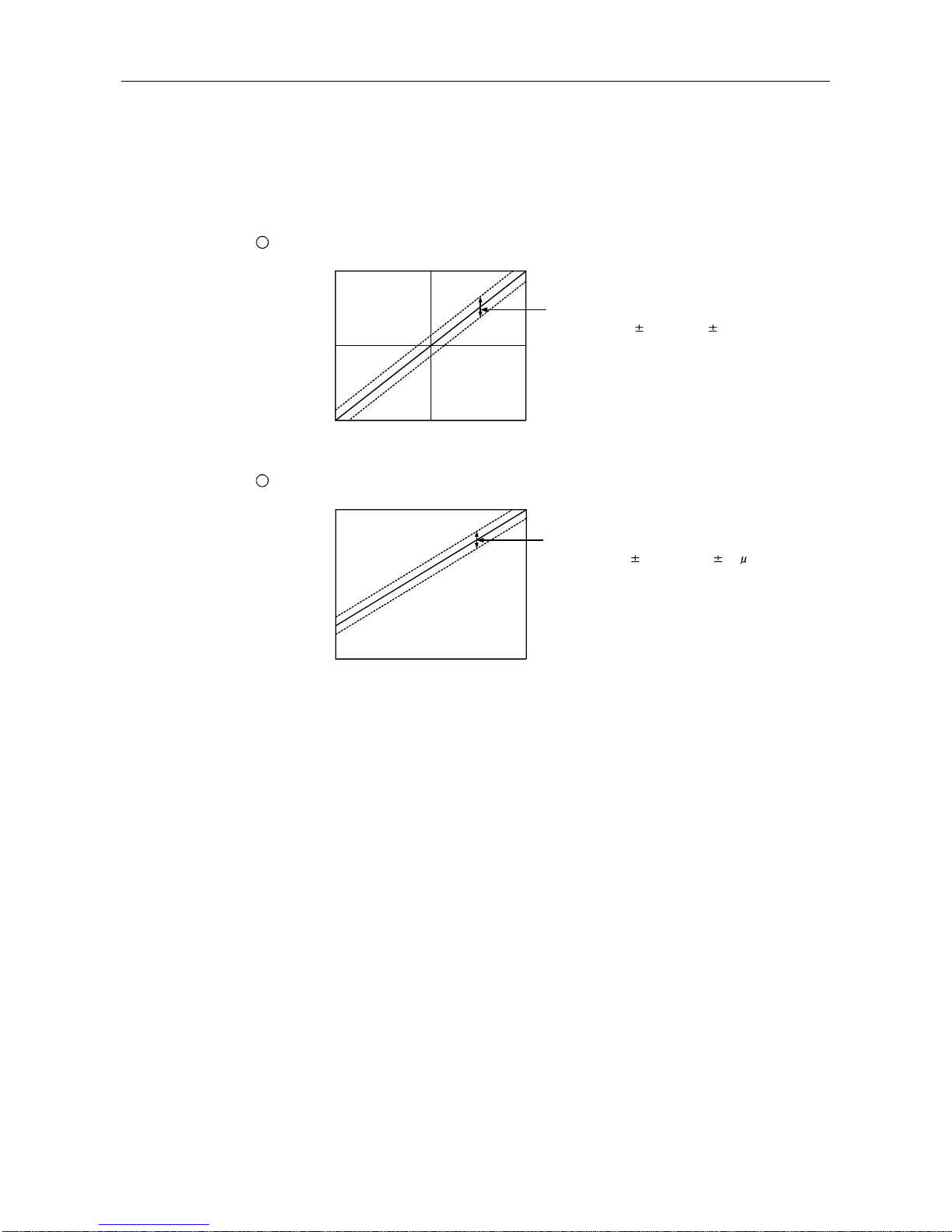
*1 Maximum resolution of analog value
The maximum resolution of analog value means the variation of analog value when the digital
value changes for "1".
*2 Total accuracy
The total accuracy is the accuracy of the maximum analog output value.
1
The overall accuracy of the AJ65BT-64 DAV is the accuracy for 10V.
0V
-10V
+10V
-2000 20000
A
n
a
l
o
g
o
u
t
p
u
t
v
a
l
u
e
Digital input value
Depending on the operating environment
(
the ambient temperature, noise), it fluctuates
within a range of 1.0% of 10V ( 100mV).
2
The overall accuracy of the AJ65BT-64 DAI is the accuracy for 20mA.
20mA
4mA
0mA
0 4000
A
n
a
l
o
g
o
u
t
p
u
t
v
a
l
u
e
Digital input value
Depending on the operating environment
(the ambient temperature, noise), it fluctuates
within a range of 1.0% of 20mA ( 200 A).
*3 Maximum conversion speed
The maximum conversion speed means the time required to read the digital value written in the
buffer memory, execute the D/A conversion, and output the specified analog value. It takes the
longest (1ms) to produce the maximum analog output value when the current output is the
minimum, and to produce the minimum analog output value when the current output is the
maximum.
3. SPECIFICATIONS MELSEC-A
3-4
3.3 I/O Conversion Characteristics
The I/O conversion characteristics of the AJ65BT-64DAV/DAI are explained.
3.3.1 Offset value and gain value
(1) Offset value
This is an analog value (voltage or current value) produced by the AJ65BT-64DAV/DAI when the
digital value set by the PLC CPU is "0".
(2) Gain value
This is an analog value (voltage or current value) produced by the AJ65BT-64DAV/DAI when the
digital value set by the PLC CPU is "2000" for AJ65BT-64DAV, and "4000" for AJ65BT-64DAI.
(3) The factory-set offset and gain values are as follows:
AJ65BT-64DAV AJ65BT-64DAI
Offset value 0V 4mA
Gain value 10V 20mA
(4) The offset value and gain value can be set separately for each channel in the test mode.
3.3.2 I/O conversion characteristics
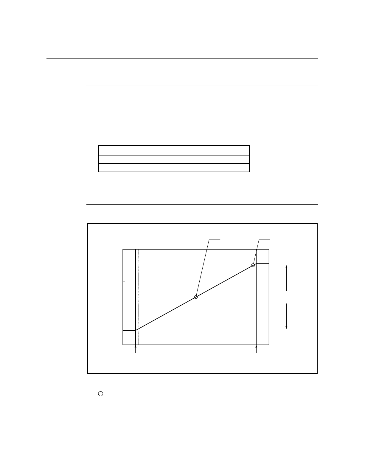
(1) When AJ65BT-64DAV is used:
15
(V)
10
5
-5
-10
-15
0
-2000
-2048
2000
2047
0
A
n
a
l
o
g
o
u
t
p
u
t
v
o
l
t
a
g
e
Offset value Gain value
Digital input value
A
nalog output
practical range
Figure 3.1 I/O conversion characteristics of the AJ65BT-64DAV
1
How to calculate the analog output value:
The resolution of AJ65BT-64DAV can be set arbitrarily by modifying the settings of the offset
value and gain value.
How to calculate the analog value resolution and the analog output value for a given digital
input value when the settings of the offset value and gain value are changed is shown next.
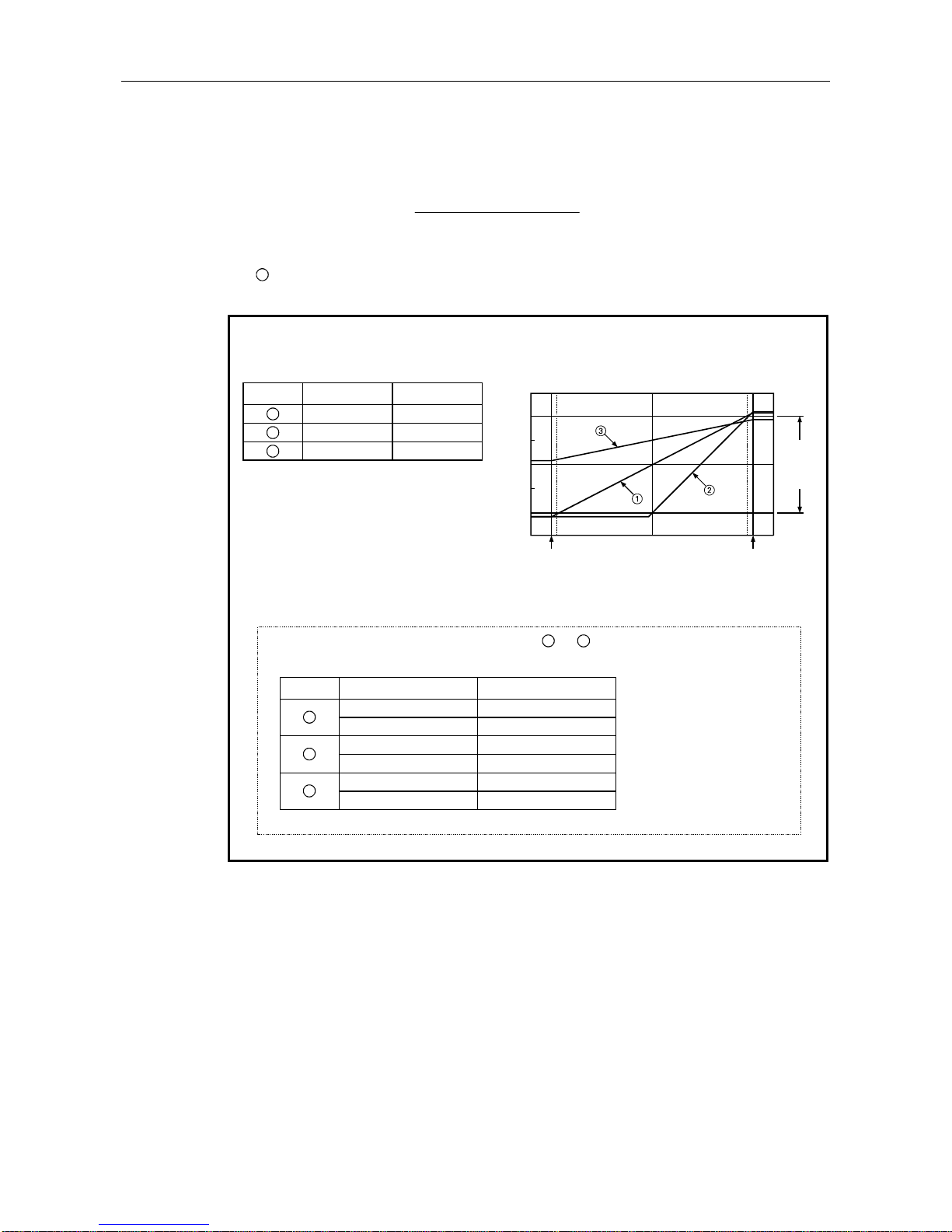
3. SPECIFICATIONS MELSEC-A
3-5
2
The following graph shows the I/O characteristics when the offset and gain values of the
AJ65BT-64DAV are changed:
15
(V)
10
5
0
-5
-10
-15
-2000
-2048
2000
2047
A
n
a
l
o
g
o
u
t
p
u
t
v
o
l
t
a
g
e
Analog
output
practical
range
Digital input value
0
Example
Figure 3.2 I/O conversion characteristics of AJ65BT-64DAV
The analog output voltage for the characteristic graphs 1 to 3 becomes as below, when the digital
input value is at 1000 and 500:
Number Digital input value Analog output voltage
1000 +5.0V
1
500 +2.5V
1000 0V
2
500 -5.0V
1000 +6.0V
3
500 +5.0V
(Analog resolution) =
2000
(Gain value) - (Offset value)
(Analog output) = (Analog resolution) × (Digital input value) + (Offset value)
The I/O conversion characteristics are shown in
the graph on the right when the offset value and
the gain value are set as in the following table:
Number Offset value Gain value
1
0V +10V
2
-10V +10V
3
+4V +8V
 Loading...