MITEL ACE9040K, ACE9040IW, ACE9040FP2N, ACE9040FP1Q, ACE9040FP1N Datasheet
...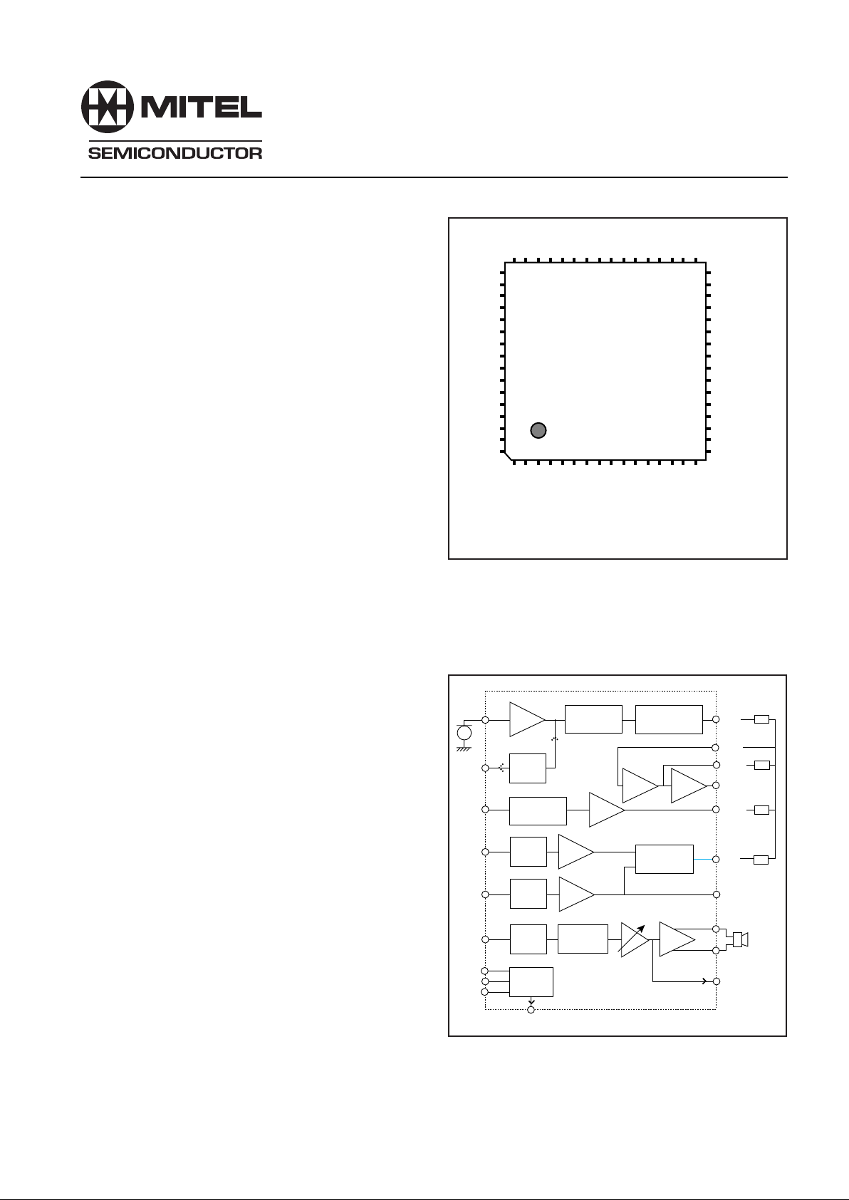
Fig.1 Pin connections - top view
Fig. 2 ACE9040 Simplified Block Diagram
Note: Pin 1 is identified by moulded spot and
by coding orientation. (* 7 x 7 mm package and
10 x10 mm package pinouts on page 3)
FP64
ACE9040 provides all the speech signal processing and
data/SAT tone filtering needed for AMPS or TACS analog
cellular telephones.
Transmit voice channel functions comprise a microphone
amplifier, soft limiter, bandpass filter, compressor, hard
limiter, lowpass filter and a gain controlled amplifier to set
deviation level. Additional transmit circuits include a DTMF
generator, data and SAT filters, deviation setting amplifiers for
data/ST and SAT and a modulation combiner.
ACE9040’s receive path comprises a bandpass filter,
expander, volume control and power amplifiers to directly
drive an earpiece or handsfree transducer.
Gain settings, mute switches and filter characteristics are
programmed via a three wire serial interface.
To implement a handsfree function, both transmit and
receive paths have rectifiers for signal amplitude monitoring
via an external pin and signal path attenuators controlled via
the serial interface.
ACE9040 combines minimum power consumption with
low external component count. Standby modes greatly reduce
supply current and extend battery charge intervals.
FP64
FEATURES
■ Low Power and Low Voltage (3·6 to 5·0 V) Operation
■ Power Down Modes
■ Direct Connections to Microphone and Earpiece
■ Compander with wide operating range:
Compressor 74 db typ., Expander 36 dB typ.
■ SAT Bandpass and Data Lowpass Filters
■ Handsfree Operation Supported
■ DTMF Generator
■ Serial Bus Controlled Gains and Filter Responses
■ Part of the ACE Integrated Cellular Phone Chipset
■ TQFP 64 Pin 10X10 mm or 7X7 mm Packages
APPLICATIONS
■ AMPS and TACS Cellular Telephones
■ Two-Way Radio Systems
RELATED PRODUCTS
ACE9040 is part of the following chipset:
■ ACE9020 Receiver and Transmitter Interface
■ ACE9030 Radio Interface and Twin Synthesiser
■ ACE9050 System Controller and Data Modem
ORDERING INFORMATION
Industrial temperature range
TQFP 64 lead 10 x 10 mm, 0·5 mm pitch
ACE9040K/IW/FP1N - devices shipped in trays and dry packed
ACE9040K/IW/FP1Q - tape mounted and dry packed
TQFP 64 lead 7 x 7 mm, 0·4 mm pitch
ACE9040K/IW/FP2N - devices shipped in trays and dry packed
ACE9040K/IW/FP2Q - tape mounted and dry packed
nc nc\DVSS*
AMPI nc\LEN*
PREIN DVSS\DVDD*
TBPO LEN\VMIDRX*
CIN DVDD\LO*
CRCIN VMIDRX\STBY*
VMIDTX LO\EVDD*
CRCOUT STBY\EPON*
nc EVDD\nc*
COUT EPON\nc*
TXC EVSS
RXC EPOP
IPS EAMPFB
SLO EAMPO
MI EIN
MICBIAS ERCOUT
VDD AMPO
DEC DTMF
HF nc
LI V485
RREF BGAP
BIAS TLPO
AVDD SUMI
DATI SUMO
TSI MOD
RSI AVSS
RXI DATO
RBPO TSO
EAMPI RSO
HFGIN SD
EOUT SCLK
ERCIN LVN
ACE9040
1
AMP
MI
MODULATION
SUMMING
AMPLIFIER
DTMF
DATI
TSI
RSI
COMPRESSOR
DATA FILTER
(LOW PASS)
GENERATE/
TRANSPOND
FILTERS AND
DEVIATION SET
DTMF
GEN.
TX SAT
FILTER
RX SAT
FILTER
RX
FILTER
SET
LEVELS
CONTROL
LOGIC
EXPANDERRXI
SCLK
LEN
SD
STBY
SET DEVIATION
VOLUME
LINE OUTPUT
LO
EPON
EPOP
RSO
TSO
DATO
MOD
SUMO
SUMI
TLPO
FEEDBACK
ABSOLUTE MAXIMUM RATINGS
Supply voltage 6 V
Storage temperature - 55 °Cto+150°C
Operating temperature - 40 °Cto+85°C
Voltage at any pin - 0.3 V to V
DD
+ 0.3 V
ACE9040
Audio Processor
Advance Information
Supersedes January 1997 edition, DS4289 - 2.5 DS4289 - 3.1 December 1997
2
ACE9040
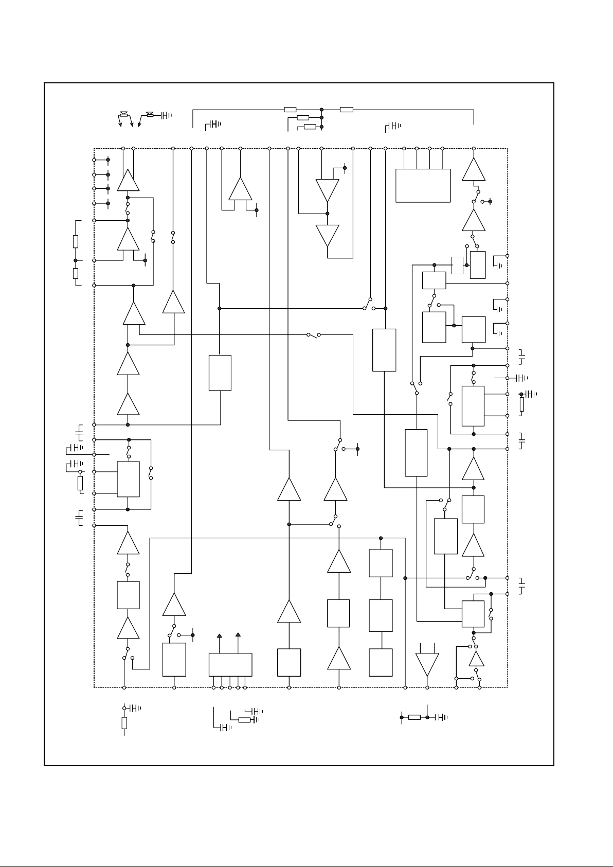
Fig. 3 ACE9040 Detailed Block Diagram
180KΩ
10nF
3.3µF
RXI
DATI
8
LOW PASS
FILTER
11
TONEM
VMIDRX
DATM
VMIDRX
VMIDTX
BIAS
GENERATOR
2
6564
44
DEC
BIAS
RREF
MICBIAS
BGAP
100/
68*kΩ
10nF
*VDD = 3.75V
RSI
10
RXSAT
FILTER
9
TSI
-12 dB / 0 dB
DTMF
47
DTMF
VDO
220 kΩ
33
LVN
_
+
Vth
VDD
4
63
LI
MLI
MI
SLO
IPS
10nF
SOFT
LIMITER
62 61
INPSENSE
DTMFM
92% DETECT
LEVEL
DTMF
MODE
PRE-
EMPHASIS
TXSAT
FILTER
-15dB
SATS
10dB
DATADEV
RXBPF
RXM
EXPGAIN
12 18 16 17 27 15
VMIDRX
33nF
RBPO EIN ERCOUT ERCIN EOUT HFGIN
EXPANDER
100nF
82nF
10nF
COMP[2:1]
SCHMITT
SATDEV
VMIDRX
3 & 97%
DETECT LEVELS
TEST [1:0]
TXBPF
HFGAIN
10nF
180kΩ
100nF
COMPRESSOR
52 53 56 54 55 58 51
TBPO CIN CRCOUT CRCIN COUT PREIN AVSS DVSS V485 EVSS
33nF
82nF
39
30 45 22
GAIN
CONTROL
TEST [2:1]
TEST [1:0]
PRE-
EMPHASIS
HANDSFREE
RECTIFIER
RXC
HFS
TXC
SD
HANDSFREE
RECTIFIER
RXLEVEL
HFATTEN
SIDETONE
LODRIVE
EARSENSE
14
EAMPI EAMPFB EAMPO
13 20 19
EAMP
_
+
VMIDRX
SUB
124728
VDD
EVDDAVDD
DVDD
21
23
EPH0/
EPH1
EPH0/EPH1
26
HIZ
38
EPOP
EPON
LO
DATO
60
50
48
_
+
VMIDTX
TXSENSE
_
+
VMIDTX
36
37
41
42
40
3
59
HARD
LIMIT
-8 dB
TEST[0]
TXLPF
TXM
VMIDTX
AUDIODEV
TLPO
DRIVER
43
TLPO
SERIAL
INTERFACE
25
29
35
34
STBY
LEN
SD
SCLK
TXC
68nF
SUMI
MOD
HF
TSO
SUMO
RSO
RXC
AMPI
AMPO
68nF
33µF
64Ω
150Ω
MIS

3
ACE9040
Pin No. Pin No. Name Description
FP2 package FP1 package
11VDDVDD supply to substrate, pin should be at highest d.c. voltage
2 2 DEC Mid-supply reference decoupling connection, 3.3 µF to GND
3 3 HF Output from TX or RX handsfree rectifier, switched by bit “HFS”
4 4 LI Line input
5 5 RREF Reference bias current set for all op-amps by resistor to GND
6 6 BIAS Buffered mid-supply reference output
77AV
DD
Analogue VDD input
8 8 DATI Transmit data input
9 9 TSI SAT path input for locally generated tone
10 10 RSI SAT path receiver input for received tone
11 11 RXI Speech path receiver input
12 12 RBPO Audio output from EXPGAIN block
13 13 EAMPI Output from EARSENSE amp
14 14 HFGIN Input to RX volume control and handsfree attenuator
15 15 EOUT Expander speech output
16 16 ERCIN Expander time constant input, 180 kΩ to ERCOUT, 100 nF to GND
17 17 ERCOUT Expander time constant output, 180 kΩ to ERCIN
18 18 EIN Expander speech input, 33 nF to RBPO
19 19 EAMPO Output from EAMP op-amp
20 20 EAMPFB Inverting input to EAMP op-amp
21 21 EPOP Earpiece driver positive output
22 22 EV
SS
Earpiece VSS (GND) supply connection
- 23/24 nc No connection
23 25 EPON Earpiece driver negative output
24 26 EV
DD
Earpiece VDD supply input
25 27 STBY Standby output: low indicates standby state, high is VDD output @ 10 mA
26 28 LO Line output
27 29 VMIDRX RX path mid-supply reference voltage, 82 nF to GND
28 30 DV
DD
Digital V
DD
29 31 LEN Serial interface latch signal input, rising edge triggered
30 32 DV
SS
Digital VSS (GND) connection
31/32 - nc No connection
33 33 LVN Low supply V
DD
voltage indicator comparator output, reset active low output
34 34 SCLK Serial interface system clock input
35 35 SD Serial interface data input
36 36 RSO Received (regenerated) SAT output
37 37 TSO Transmit SAT output, regenerated or transponded
38 38 DATO Transmit data filter output.
39 39 AV
SS
Analogue VSS (GND)
40 40 MOD Modulation output: sum of Speech, Data and SAT
41 41 SUMO Modulation summing amplifier output
42 42 SUMI Modulation summing amplifier input
43 43 TLPO Transmit audio lowpass filter output
44 44 BGAP Bandgap voltage output, 10 nF to GND
45 45 V485 Hard limiter gain selection for 3.75 V or 4.85 V nominal supplies
46 46 nc No connection
47 47 DTMF DTMF tone output
48 48 AMPO Auxillary op-amp output
49 49 nc No connection
50 50 AMPI Auxillary op-amp inverting input (non-inverting internally connected to VMIDTX)
51 51 PREIN Transmit pre-emphasis filter input
52 52 TBPO Transmit bandpass filter output
53 53 CIN Compressor audio input, 10 nF from TBPO
54 54 CRCIN Compressor time constant input, 100 nF to GND, 180 kΩ to CRCOUT
55 55 VMIDTX TX path reference voltage, 82 nF to GND
56 56 CRCOUT Compressor time constant output, 180 kΩ to CRCIN
57 57 nc No connection
58 58 COUT Compressor audio output, 33 nF to PREIN
59 59 TXC Transmit handsfree audio level sensing rectifier smoothing filter, 68 nF to GND
60 60 RXC Received handsfree audio level sensing rectifier smoothing filter, 68 nF to GND
61 61 IPS Transmit audio gain INPSENSE adjustment block input
62 62 SLO Soft limiter output
63 63 MI Microphone input
64 64 MICBIAS Bias for electret or active microphone
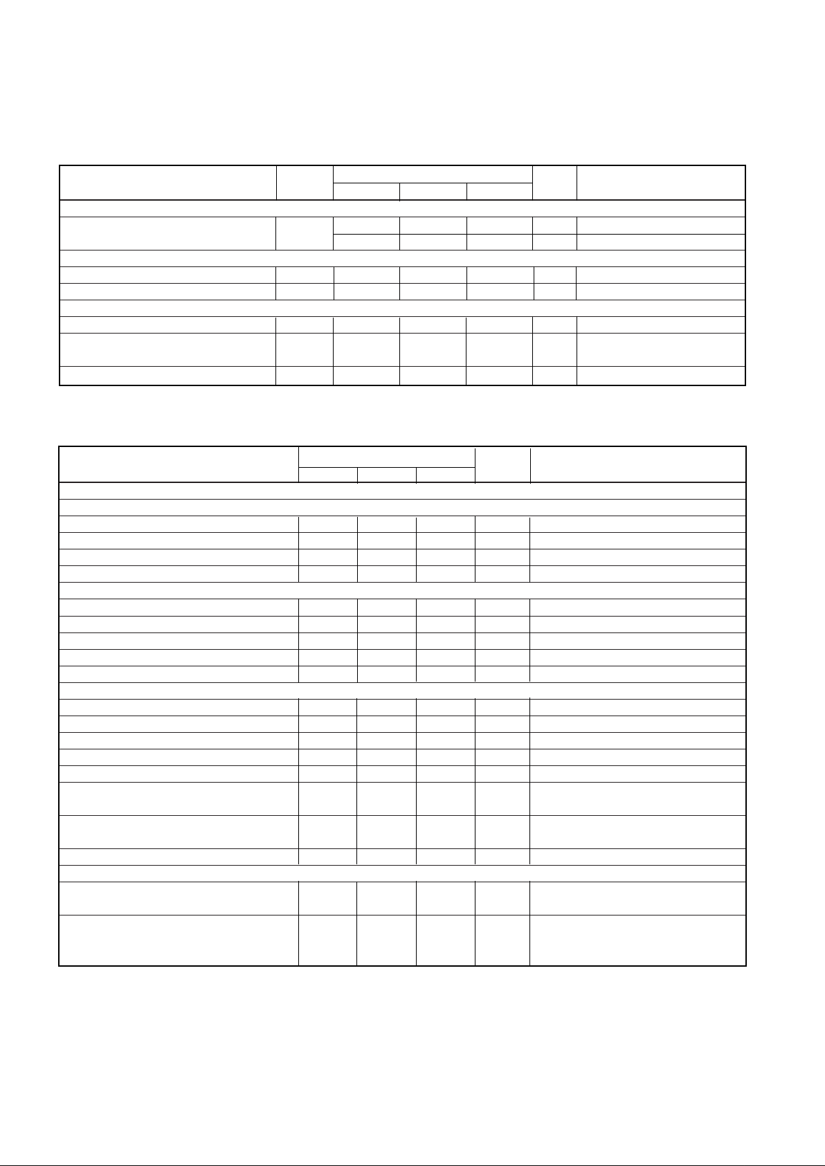
PIN DESCRIPTIONS
Note: FP1 = 10 x 10mm package, FP2 = 7 x 7 mm package
4
ACE9040
Characteristic Symbol Value Unit Conditions
Min. Typ. Max.
Supply Current and Power Down Modes
Operating supply current I
DD
15 mA VDD = 4.85 V R
REF
= 100 kΩ
15 mA VDD = 3.75 V R
REF
= 68 kΩ
Standby
Attenuation of all inputs signals 40 dB
Wakeup response time 10 ms
Sleep (Standby with CLK stopped)
Supply current* I
DD(SLEEP)
200 µA STBY bit set VDD = 3.75
Delay between setting STBY bit and 20 µs
stopping clock
Delay to starting clock after wakeup 100 µs
Characteristic Value Unit Conditions
Min. Typ. Max.
Transmission Path
Microphone Amp, MI to SLO pins
Input bias VDD/2 Internal 150 kΩ bias resistor to VDD/2
Microphone input gain (LO) 21 22 23 dB MIS = 1, MLI = 0, MIG = 0
Microphone input gain (HI) 31 32 33 dB MIS = 1, MLI = 0, MIG = 1
Microphone crosstalk (no MI signal) – 40 dB MIS = 1, MLI = 0, MIG = 1
Line input, LI to SLO pins
Input bias VDD/2 Internal 100 kΩ bias resistor
LI input Gain (0dB) – 0.5 0.5 dB MIS = 0, MLI = 0, MIG = 0
LI input Gain (LO) 21 22 23 dB MIS = 1, MLI = 1, MIG = 0
LI input gain (HI) 31 32 33 dB MIS = 1, MLI = 1, MIG = 1
LI input crosstalk (no LI signal) – 40 dB MIS = 1, MLI = 1, MIG = 1
Soft Deviation Limiter, LI to SLO pins
Nominal gain 0 dB Limiter not functioning.
Attenuation range – 30 – 29 dB
Attenuation steps 0.27 0.5 0.67 dB
Distortion 2 %THD Output at 1 Vrms
Attack level:Hard limiter output 3 97 % V
DD
Attack level at TBPO pin 92 % VDDd.c. input at IPS
TEST[1:0] = 11
Attack time 40 µs Per gain step when signal outside
threshold
Decay time 1.68 ms Per gain step
INPSENSE Gain Stage, IPS to TBPO pins
Nominal gain 7.5 8 8.5 dB Input = 100 mV
rms,
INPS[4:0] = 15, THF = 0 dB,
Gain adjustment range – 12 12.8 dB Relative to nominal gain
Input = 100 mV
rms,
Gain step size 0.6 0.8 1.2 dB INPS[4:0] = 0 to 31, THF = 0 dB
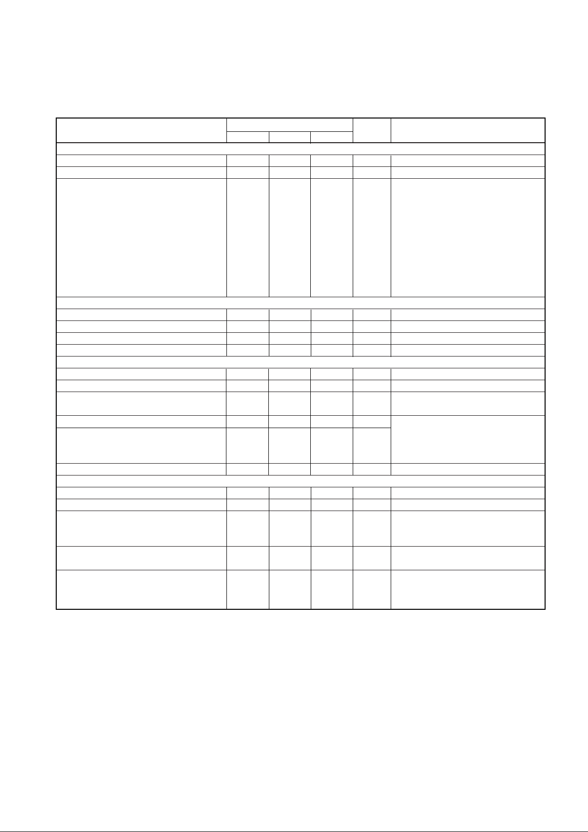
ELECTRICAL CHARACTERISTICS
These characteristics are guaranteed over the following conditions unless otherwise stated (Note 1):
T
AMB
= – 40 °C to + 85 °C, VDD = 3.6 V to 5.0 V
Note 1. 100% production tested at 25 °C but guaranteed over specified temperature range.
* Standby current measured with the 1.008 MHz clock stopped and SCLK at a level <200 mV.
5
ACE9040
Characteristic Value Unit Conditions
Min. Typ. Max.
TX Audio Bandpass Filter TXBPF, IPS to TBPO
Noise – 72 dBV
Distortion 1 %THD 1 Vrms output
Frequency response relative to 1040 Hz – 60.5 – 38.5 dB f = 60 Hz
– 25.5 – 10.5 dB f = 184 Hz INPSENSE = 0 dB
– 1.0 + 0.5 dB f = 430 Hz THF = 0 dB
– 0.5 + 0.5 dB f = 676 Hz, 1040 Hz
– 0.5 + 0.5 dB f = 1410 Hz, 1900 Hz
– 1.5 – 0.5 dB f = 3260 Hz
– 3.0 – 1.5 dB f = 3500 Hz
– 10.5 – 5 dB f = 4120 Hz
– 20.5 – 15.5 dB f = 5590 Hz
– 90.5 – 30.5 dB f = 9900 Hz
TX Handsfree Gain Stage HFGAIN
Nominal gain 0 dB
Gain range – 52.5 – 49 – 45.5 dB THF[2:0] = 0 to 7
Gain step size 6.5 7 7.5 dB 0 to –21 dB
Gain step size 5 7 9 dB –28 to –49 dB
TX Compressor Stage, CIN to COUT pins
Unity gain level 636 707 777 mVrms = Vref (Unaffected level)
Input range 0.79 1000 mVrms
Linearity CIN to COUT: ± 0.5 dB CIN = Vref + 3 dB to Vref - 59 dB
(Deviation from 2:1 I/O relationship) BW = 300 Hz to 3.4 kHz
Attack time 3 ms 12 dB step: - 8 dB to - 20 dB relative
to the unity gain (Vref) level
Decay time 13.5 ms Attack & Decay levels = 1.5 and 0.75
of steady state final value
Distortion 2 %THD BW = 300 Hz - 3.4 kHz
Frequency response ± 0.2 dB BW = 300 Hz - 3.4 kHz
TX Pre-emphasis, PREIN to TLPO pins
Input impedance 75 kΩ
Internal compressor and BAR:
Nominal gain TACS – 7.5 – 7 – 6.5 dB COMP[2:1] = 10 or 01 at 1 kHz
Nominal gain AMPS – 11.5 – 11 – 10.5 dB
External compressor and bypass:
Nominal gain AMPS & TACS – 0.5 0 + 0.5 dB COMP[2:1] = 11 or 00 at 1 kHz
Frequency response 5.8 6 6.2 dB/ TEST[1:0] = 01
Octave PREEMPH = 0 (active)
f = 300 to 3400 Hz
ELECTRICAL CHARACTERISTICS
These characteristics are guaranteed over the following conditions unless otherwise stated (Note 1):
T
AMB
= – 40 °C to + 85 °C, VDD = 3.6 V to 5.0 V

6
ACE9040
Characteristic Value Unit Conditions
Min. Typ. Max.
Hard Deviation Limiter
Gain 13 13.5 14 dB V485 pin = 0 V (for V
DD
= 3.75 V)
15.5 16 16.5 dB V485 pin = VDD (for VDD = 4.85 V)
Low Pass Filter TXLPF, PREIN to TLPO pins
Distortion 1.5 %THD 1.5 Vp-p Output level
Noise – 60 dBV BW = 30 Hz to 30 kHz
Frequency response TACS/AMPS 0.3 0.7 dB f = 307 Hz
Relative to 1 kHz – 0.5 + 0.5 dB f = 676 Hz, 1040 Hz
– 0.5 + 0.5 dB f = 1410 Hz, 1900 Hz
– 3.0 – 1.5 dB f = 3010 Hz
– 38.0 – 13.0 dB f = 3500 Hz
– 60.0 – 38.0 dB f = 4120 Hz
– 60.0 – 38.0 dB f = 5590 Hz
– 60.0 – 38.0 dB f = 9900 Hz
– 60.0 – 35.0 dB f = 11870 Hz
– 60.0 – 35.0 dB f = 14950 Hz
Gain – 8.5 – 8 – 7.5 dB
Attenuation with TXLPF bypassed 8 dB TEST[0] = 1
Gain Stage AUDIODEV, PREIN to TLPO
Nominal gain 0 dB Output at TLPO
Gain adjustment - 2.8 3.2 dB
Attenuation step size 0.2 0.4 0.6 dB Control bits: AUDEV[3:0]
TXM switch attenuation – 60 dB AUDIODEV = 0 dB
Combined TX path
Gain with 3.5 µV at Microphone input 33.5 37.5 dB INSENSE = 0 dB, V485 = 0 V
Distortion 1.0 % THD THF & AUDIODEV = 0 dB
Noise – 55.0 dBV MI gain = 22 dB, V
DD
= 3.6 V
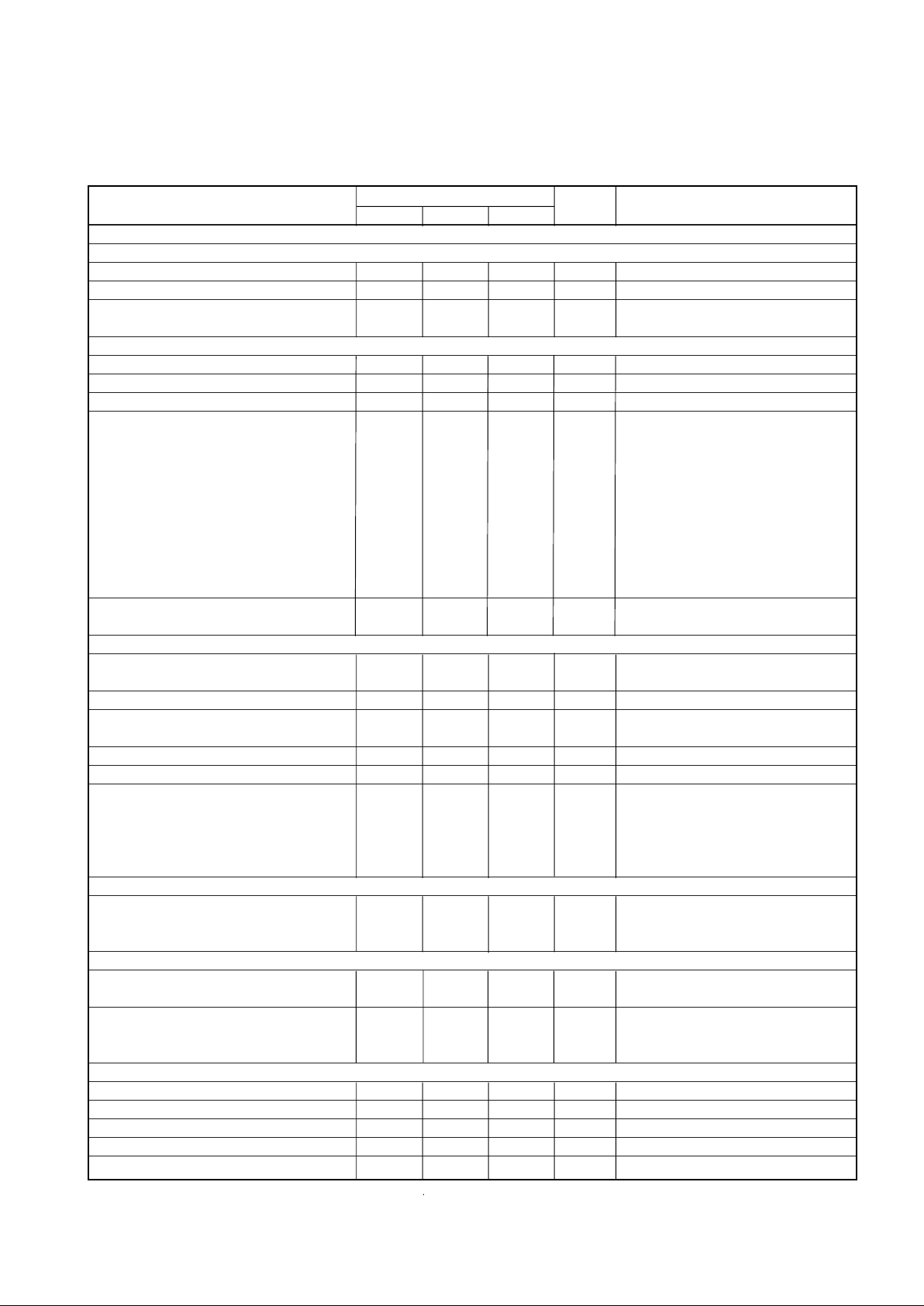
Output d.c. level 1.65 1.9 V Compressor Bypassed
ELECTRICAL CHARACTERISTICS
These characteristics are guaranteed over the following conditions unless otherwise stated (Note 1):
T
AMB
= – 40 °C to + 85 °C, VDD = 3.6 V to 5.0 V
–
7
ACE9040
ELECTRICAL CHARACTERISTICS
These characteristics are guaranteed over the following conditions unless otherwise stated (Note 1):
T
AMB
= – 40 °C to + 85 °C, VDD = 3.6 V to 5.0 V
Characteristic Value Unit Conditions
Min. Typ. Max.
Receive Path
RX Input stage RXSENSE, RXI to RBPO pins
Input bias VDD/2 Internally biased to VDD/2 by 150 kΩ
Nominal gain 7.25 8 8.75 dB
Gain adjustment range – 6 6.4 dB Input 40 mVrms at RXI
Gain adjustment step size 0.2 0.4 0.6 dB RXM = 1, RXSENSE = 0 to 31
RX Audio Bandpass Filter RXBPF
Gain 0 dB
Distortion 1 %THD At 1 kHz with 40 mVrms input
Noise – 65 dB BW= 30 Hz to 30 kHz
Frequency Response – 90.0 – 45.0 dB f = 60 Hz RXSENSE = 0 dB
Relative to 1040 Hz – 15.0 – 7.0 dB f = 184 Hz COMP[1:0] = 00
– 2.0 + 0.5 dB f = 430 Hz
– 0.5 + 0.5 dB f = 676 Hz, 1040 Hz
– 0.5 + 0.5 dB f = 1410 Hz, 1900 Hz
– 3.0 – 0.5 dB f = 3260 Hz
– 10.0 – 6.0 dB f = 3500 Hz
– 40.0 – 25.0 dB f = 4120 Hz
– 40.0 – 25.0 dB f = 5590 Hz
– 90.0 – 40.0 dB f = 9900 Hz
RXM mute switch attenuation – 40 dB Output switched to V
DD
/2 when
muted.
Rx Internal Expander
Gain EXPGAIN: internal 11.8 12.3 12.8 dB COMP[2:1] = 10
external and bypass 0 dB COMP[2:1] = 00 or 11
Unity gain level 850 1000 1100 mVrms = Vref (Unaffected level)
Linearity EIN to EOUT ± 1 dB EIN = Vref to Vref - 33 dB
(Deviation from 2:1 input/output) BW = 300 to 3400 Hz
Distortion 2 %THD 1 Vrms
Frequency response ± 0.2 dB 300 to 3400 Hz
Attack time 3 ms 6 dB step (- 4 dB and -10 dB) relative
to the unity gain (Vref) level at 1 kHz
to pin EIN. Output at EOUT.
Decay time 13.5 ms Attack and delay time levels = 0.57
and 1.5 of final steady state value.
RX Volume Control RXLEVEL
Nominal Gain – 11 – 12 – 13 dB RXV[2:0] = 3, RHF = 0 dB
Gain adjustment range – 9 12 dB RXV[2:0] = 0 to 7
Gain adjust step size 2 3 4 dB EARSENSE = 0 dB, Sidetone = 0 dB
RX Handsfree Gain Stage HFATTEN
HFGAIN to EAMP nominal gain – 0.4 0 0.4 dB RHF, RVX, EARSENSE = 0 dB,
SD =0
Gain range – 52.5 – 49 – 45.5 dB RHF[2:0] = 0 to 7
Gain control step size 6.5 7 7.5 dB 0 to – 21 dB
Gain control step size 5 7 9 dB – 28 to – 49 dB
RX Line Driver LODRIVE
LO gain 4 5 6 dB RVX = 0 dB, RHF = 0 dB, HIZ =1
Distortion 2 %THD 1.0 Vrms output
LO mute – 40 dB HIZ = 0
Noise – 80 dBV BW = 30 Hz to 30 kHz
LOoutput during mute 1.5 V
DD
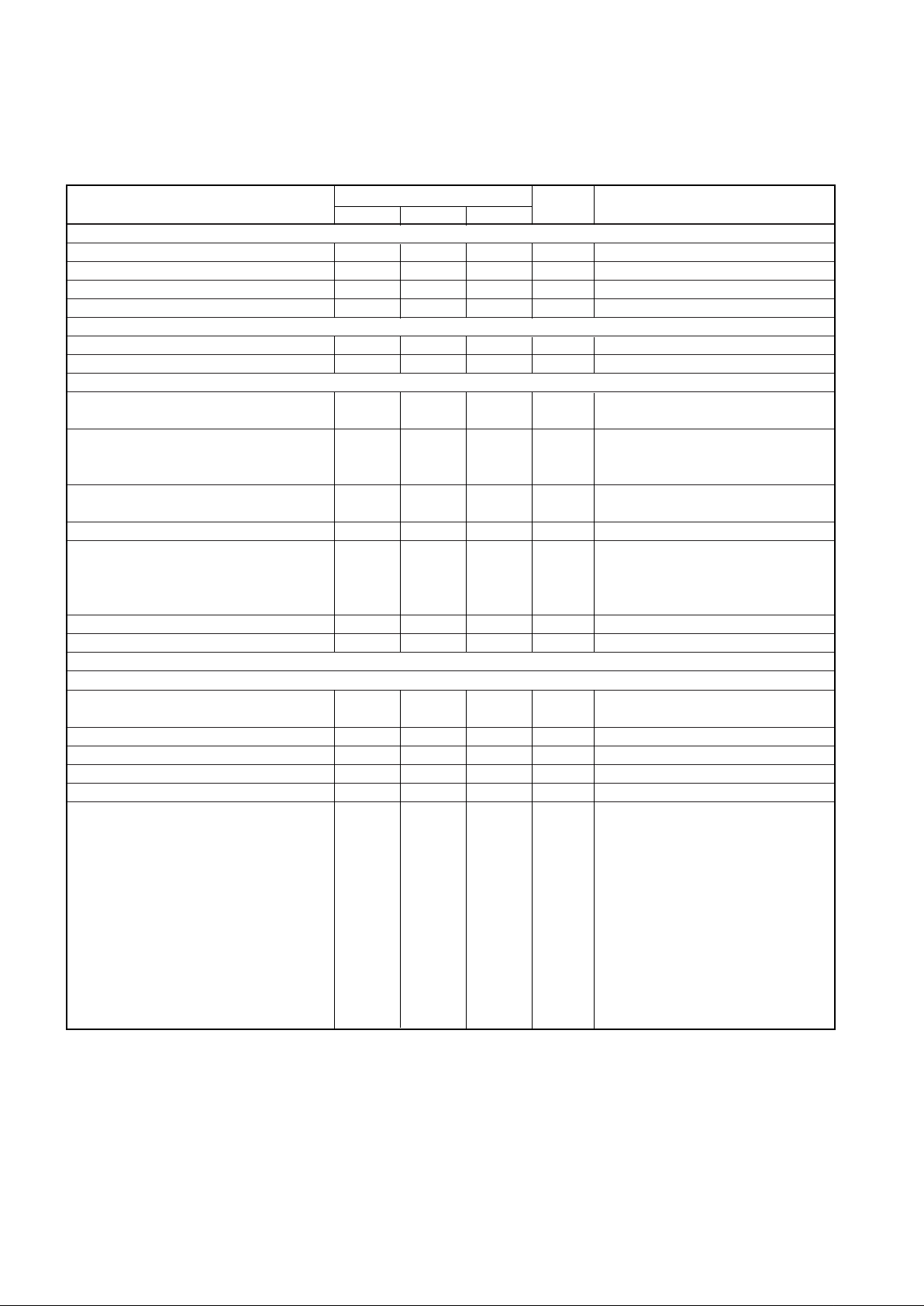
/2 2.1 V VDD = 3.6 V
8
ACE9040
Characteristic Value Unit Conditions
Min. Typ. Max.
Rx Earpiece Gain Adjustment EARSENSE
Nominal gain 0 dB
Total gain - 2.8 3.2 dB EARS[3:0] = 0 to 15
Gain adjustment step size 0.2 0.4 0.6 dB RVX = 0 dB, RHF = 0 dB, SD = 0
Distortion 1 % THD Output 1 Vrms
Rx Sidetone Path, IPS to EAMPI
Attenuation at EARSENSE amp input 18 19 20 dB EARSENSE = 0 dB
Sidetone mute – 40 dB SD = 0
Rx Earpiece Drivers EPOP & EPON
EPON single ended gain 5.5 6 6.5 dB Output = 2 Vpp,
120 Ω EPON to EPOP
EPOP single ended d.c. level 1.7 V
DD
/2 1.9 V VDD = 3.6 V, EPH1 = 1, EPH0 = 0
EPOP single ended a.c. level – 20 dB
EPON single ended distortion 1 % THD Output = 2 Vpp
EPON & EPOP differential gain 11.5 12 12.5 dB 150 Ω (± 20 %) EPON to EPOP
EPOP differential distortion 1 %THD Output = 4 Vpp, EPH1 = 1, EPH0 = 1
Earpiece mute switch attenuation 40 dB EPH0 = 0 & EHP1 = 0
EPON external mode: 64 Ω (± 20 %) + 3.3 µF to GND,
EPON gain relative to EAMPI 5.5 6.5 dB EAMPFB open, Input = HFGIN
EPON distortion 1 % THD Output = 1.1 Vpp
EPOP output current external mode – 10 10 µA At VDD & 0 V
EPON & EPOP mute – 40 dB EPH1 = 0, EPH0 = 0
EPOP Noise – 80 dBV EPH1 = 1, EPH0 = 1
Transmit Data Path
TX Data Filter 16 kHz & 20 kHz
Input bias at DATI V
DD
/2 V Internally tied via 800 kΩ resistor to
VDD/2.
Nominal gain - 6.5 - 6 - 5.5 dB Input = 1 Vrms
Distortion 1.5 %THD Output = 1.5 Vp-p
Noise -60 dBV BW = 30 Hz to 30 kHz
DATM mute switch attenuation 40 dB
Data Filter frequency response
16 kHz (TACS) – 0.3 0.3 dB f = 676 Hz, 1040 Hz
– 0.3 0.3 dB f = 4120 Hz
– 0.1 – 0.7 dB f = 12120 Hz
– 0.9 – 1.6 dB f = 13960 Hz
– 2.5 – 1.5 dB f = 14950 Hz DATM = 1
– 5.0 – 2.0 dB f = 16050 Hz DATADEV = 0 dB
– 5.0 – 3.0 dB f = 16420 Hz Relative to 1040 Hz
– 6.0 – 4.0 dB f = 17040 Hz DATAF[1:0] = 10
– 7.0 – 5.0 dB f = 18020 Hz
– 11.0 – 9.0 dB f = 19990 Hz
– 12.0 – 10.0 dB f = 20970 Hz
ELECTRICAL CHARACTERISTICS
These characteristics are guaranteed over the following conditions unless otherwise stated (Note 1):
T
AMB
= – 40 °C to + 85 °C, VDD = 3.6 V to 5.0 V

9
ACE9040
ELECTRICAL CHARACTERISTICS
These characteristics are guaranteed over the following conditions unless otherwise stated (Note 1):
T
AMB
= – 40 °C to + 85 °C, VDD = 3.6 V to 5.0 V
Characteristic Value Unit Conditions
Min. Typ. Max.
TX Data Filter 16 kHz & 20 kHz (continued)
Data Filter frequency response
20 kHz (AMPS) – 0.3 0.3 dB f = 676 Hz, 1040 Hz
– 0.3 0.3 dB f = 4120 Hz, 16050 Hz
– 0.3 – 1.5 dB f = 16050 Hz
– 2.5 – 1.0 dB f = 18020 Hz
– 3.0 – 1.5 dB f = 18880 Hz DATAF[1:0] = 11
– 4.0 – 2.0 dB f = 20240 Hz DATM = 1
– 5.0 – 3.0 dB f = 20540 Hz DATADEV = 0dB
– 5.5 – 3.5 dB f = 20970 Hz Relative to 1040 Hz
– 7.0 – 5.0 dB f = 21960 Hz
– 8.0 – 6.0 dB f = 22820 Hz
– 10.0 – 8.0 dB f = 24050 Hz
TX Data Gain Stage DATADEV, DATI to DATO pins
Nominal gain 0 dB
Gain adjustment - 2.8 3.2 dB DATD[3:0] = 7
Gain adjustment steps 0.2 0.4 0.6 dB DATM = 1 DATAF[1:0] = 00
TXSAT and RXSAT Bandpass Filters 6 kHz
RXSAT Filter
RXSAT gain 9 11 dB Input = 400 mVrms at 6030 Hz,
SATDEV = 0 dB, SATM = 1,
SATS = 0dB
RXSAT 6 kHz frequency response – 90.0 – 35.0 dB f = 2520 Hz Relative to 6030 Hz
– 90.0 – 35.0 dB f = 3500 Hz SATS = 0 dB,
– 90.0 – 35.0 dB f = 4120 Hz TACS = 1,
– 29.0 – 24.0 dB f = 4980 Hz SATD = 15 (0 dB),
– 0.30 0.50 dB f = 5900 Hz SATM = 1
– 0.10 0.35 dB f = 5960 Hz
– 0.10 0.35 dB f = 6030 Hz
– 0.30 0.50 dB f = 6090 Hz
– 26.5 – 22.0 dB f = 7010 Hz
– 90.0 – 29.0 dB f = 8060 Hz
– 90.0 – 35.0 dB f = 9040 Hz
– 90.0 – 35.0 dB f = 9290 Hz
RSO Schmitt output 5.5 6.0 6.5 kHz SATS = 0 dB, TACS = 1

10
ACE9040
Characteristic Value Unit Conditions
Min. Typ. Max.
TXSAT Filter 6 kHz
TXSAT gain – 29.0 – 25.0 dB TACS =1, SATS = 1, Output = 1 Vpp
at 6030 Hz
TXSAT 6 kHz frequency response – 90.0 – 35.0 dB f = 2520 Hz Relative to 6030 Hz
– 90.0 – 35.0 dB f = 3500 Hz SATS = 1
– 90.0 – 35.0 dB f = 4120 Hz TACS = 1
– 29.0 – 24.0 dB f = 4980 Hz SATD = 15 (0 dB)
– 0.30 0.50 dB f = 5900 Hz SATM = 1
– 0.10 0.35 dB f = 5960 Hz
– 0.10 0.35 dB f = 6030 Hz
– 0.30 0.50 dB f = 6090 Hz
– 26.5 – 22.0 dB f = 7010 Hz
– 60.0 – 35.0 dB f = 8060 Hz
– 60.0 – 35.0 dB f = 9040 Hz
– 80.0 – 35.0 dB f = 9290 Hz
TXSAT Noise – 71.0 dBV
Gain Stage SATDEV
Nominal gain 0 dB
Gain adjustment range - 4.5 4.8 dB SATS = 0, TACS = 1, SATM = 1
Gain adjustment size 0.05 0.3 0.55 dB SATD[4:0] = 0 to 31
Distortion 2 % THD Output = 1.1 Vpp
SATM switch mute attenuation 40 dB SATM = 0
DTMF Generator
DTMF output level 60 85 mVrms VDD = 3.6 V, high & low tone
DTMF single tone distortion:
TONEM switch on (via TBPO) 5 % THD Low group, TONEM = 1
TONEM switch off – 40 dB TONEM = 0
DTMF switch on (via RBPO) 5 % THD High group, DTMFM = 1
DTMF switch off – 40 dB DTMFM = 0
DTMF high group pre-emphasis – 0.5 0.5 dB DTWIST = 0
1.5 2.5 dB DTWIST = 1
Gain Stage TXSENSE, SUMI to MOD pins
Gain - 0.5 0 0.5 dB Output at MOD.
Gain adjustment - 2.8 3.2 dB TXSEN[3:0] = 0 to 15
Gain adjustment step size 0.2 0.4 0.6 dB
Distortion 2 %THD Output = 1 Vrms
Noise – 80 dBV BW = 30 Hz to 30 kHz
ELECTRICAL CHARACTERISTICS
These characteristics are guaranteed over the following conditions unless otherwise stated (Note 1):
T
AMB
= – 40 °C to + 85 °C, VDD = 3.6 V to 5.0 V
 Loading...