

Page 1
VHF
(WIDE
BAND)
SERVICE
MANUAL
LAND MOBILE RADIO
1690
North
Kansas
Topping Avenue
City,
Missouri
bUVUUU
64120
MANUAL
09-342/442 XL
SM-8/86-1.5M
NO.
70-342442
Page 2
PREFACE
70-342https://manualmachine.com/442~~
This service manual
the 70-342XL and 70-442XL transceivers. In the first section of this
manual, after transceiver description and specifications, instructions
for transceiver preparation
stallation, and summaries of available support equipment.
The second section of this service manual, entitled SERVICING,
dedicated to transceiver repair. Troubleshooting flow charts for
locating likely problem
General information follows, such
replacement instructions and realignment procedures.
Transceiver circuitry
herein respectively. Each PC board
diagrams;
Each schematic page has
be vi.ewed with
Because the PC boards have components and plating on both sides,
layout diagrams show superimposed images of plating patterns and
respective other-side-component maps. Any double-image layout of the
three PC boards can be viewed with their respective schematic without
turning pages.
all
of which can be viewed with their respective schematics.
it.
is
intended to facilitate set-up and service of
are
found-- programming, calibration, ir-
areas
is
contained on three PC boards and categorized
a
list
are
in the beginning of t-his section.
as
chip component identification and
is
detailed in text, charts, and
of other applicable diagrams that can
is
,
Information in this book
of the variety of readers' requirements, details of option add-ons
are
OPTIONS,
each add-on kit.
As
buted on the following forms:
Many useful facts and tips
intends to service several of the transceivers described herein,
spending
not included.
is
provided for allocating technical literature acquired with
necessary, service manual supplements
Manual Addition (MA)
Change Notice (CN)
Manual Correction (MC)
Technical Bulletin (TB)..For solutions to field problems and tips
time
to read applicable text
is
A
divider
.....
......
focused on the basic transceiver. Because
at
the end of this book, entitled
will
For supplemental information useful in
product alignment, service, or improvement. Printed on BLUE paper.
For circuitry change details made during
production by model and
Printed on YELLOW paper.
...
For correcting literature errors not
related to production changes. Printed
on GREEN paper.
for performance improvement. Print.ed on
PINK paper.
are
provided in the text. If the reader
will
be published and distri-
save
time
serial
in the end.
number.
Page 3
TABLE
OF
Preface
Table of Contents
Description 3
Specifications:
ElPROM Programming:
Transceiver Calibration:
Installation:
Automotive Receiver Interference 31
Optional Accessories
Service Equipment 37
Service Tools
Optional Feature Add-on Kits 39
CONTENTS
.................................................
.......................................
70-342https://manualmachine.com/442~~
PAGE
ii
1
.............................................
General
Transmit
Receive
Scan and CTCSS
Programmable Parameters
H1
Version Programmer Software 10
ElPROM Module Removal
Programming
Set-up
Error Codes
Procedure 20
Instructions 22
Under-Dash Configuration 24
Trunk-Mount Configuration
Under-Dash Power/Accessory Plug 26
Trunk-Mount Power and Accessory Plugs 28
.............................................
............................................
.............................................
......................................
.............................
......................
...............................
.........................................
..............................................
.........................................
...........................................
........................................
............................
...........................
.....................
...............
........................
....................................
.......................................
...........................................
4
5
6
7
9
10
11
18
19
25
35
38
............................
SERVICING
Troubleshooting Charts:
General 45
CPU/Phase-Lock-Loop
Transmitter
Modulator
Receiver
Component Replacement:
Chip Component Identification
Replacing Components with Leads
Chip Capacitor and Resistor Replacement
Complete Alignment:
Set Up 53
Error Codes
Realignment
Factory Presets
.............................................
.................................
.........................................
...........................................
............................................
.......................
.....................
.............
..............................................
.........................................
.........................................
.....................................
continued
46
47
47
48
49
50
51
55
55
60
......
Page 4
SERVICING continued:
Circuit Analysisf
Transmitter Board
Microprocessor Pinouts Chart
RF Power Amplifier Board
Receiver Board
Simplified Squelch Circuit Schematic
Metering
Block Diagram 77
Under-Dash Circuitry:
Under-Dash Interconnect Diagram
Front Panel Schematic Diagram
Front Panel PCB Layouts
70-342XL/442X~ Receiver PCB Layouts
DC Voltages
70-342XL Receiver Board Schematic Diagram
Trunk-Mount Circuitry:
Trunk-Mount Interconnect Diagram
Control Head
Control-Cable Interface Board
DC Voltages - Receiver Board
70-442XL Receiver Board Schematic Diagram
Transmitter Board:
DC Voltages - Transmitter Board
Microprocessor Pinouts (Duplicate Chart) 89
RF Power Amplifier PCB Layout 90
E/PROM Module Layout 90
Transmitter PCB Layouts
Transmitter
Under-Dash Exploded Mechanical
70-2301 Microphone
70-2195 Hang Up Box
Trunk-Mount Exploded Mechanical
Parts List 97
Parts Ordering 109
................................................
...........................................
..............................................
..........................................
...................................
........................
............................
......................................
....................
.....................
.......................
.............................
.................
-
Receiver Board
........................
...........
....................
........................................
.......................
........................
...........
.....................
............
.......................
................................
.............................
Board Schematic Diagram
View
Detail
Detail
...............................
..............................
View
.................
.....................
....................
61
63
69
71
75
76
78
80
81
82
83
83
84
85
86
87
87
88
91
93
94
95
95
96
OPTIONS
...................
Page 5
GENERAL DESCRIPTION
The MIDLAND SYN-TECH 70-342XL and 70-442XL VHF wide-band Land-Mobile
transceivers are mobile two-way radios designed to operate on FM
channels between 136 to 174 MHz. There are two varieties of the SYNTECH 70-342XL and 70-442XL transceivers, each designed to operate on
different channel frequency range: the A-band radios (70-342AXL
442AXL) on the 136-163 MHz range; the B-band radios (70-342BXL
442BXL) on the 148-174 MHz range. SYN-TECH transceivers have the
capacity to operate on up to eighty operator selectable channels, each
of which can be programmed in the service shop.
is
The SYN-TECH 70-342XL transceiver
It
ing.
panel for easy access to the operator. The SYN-TECH 70-442XL transceiver
location.
pin
receptacle
long Control Cable that interconnects the 70-442XL remote unit with
its
Control Head. The Control Head contains all the operator controls
and
operator.
As
the SYN-TECH 70-342 and 70-442 transceivers, the XL models are
wide-band radios. Electronic tuning of critical stages
allow them to operate over a 24 MHz spread of channel frequencies.
has a control knobs, push buttons, and display all on a front
is
configured for mounting in a vehicle trunk or other remote
It
does not have front panel controls; instead
in
its
face-piece. The receptacle accepts the 4-meter
is
much smaller in size for mounting where accessible by the
configured for under-dash mount-
70-342https://manualmachine.com/442~~
&
&
it
has a 34-
is
used to
a
70713-
It
5
A
is
is
The XL models are revised 70-342 and 70-442 transceivers that used
KHz for their main VCO comparator frequency. The 70-342XL and 70442XL models use 2.5 KHz, thus allowing channel frequency increments
of 2.5 KHz for half-channels.
as
Many optional features, such
Complete add-on kits for field installation are readily available.
listing
Operating parameters such
and a variety of feature timing and codes
in an alterable memory module for easy customizing. The plug-in
memory module
E/PROM Programmer.
The 70-342XL and 70-442XL transceivers contain three major printed
circuit boards. The Transmitter Board contains transmitter, synthesizer, and microprocessor control circuitry.
components facing up, on the top side of the chassis center divider.
The Receiver Board also lays horizontally, but on the underside of the
chassis divider with components facing down. The third PC board
the RF Power Amplifier Board located inside the rear heat sink.
accessible by removal of the heat sink top cover.
with
brief kit descriptions can be found in later sections.
as
channel frequencies, CTCSS frequencies,
is
reprogrammable in the service shop using the MIDLAND
CTCSS, can be added at the factory.
are
electronically contained
It
lays horizontally, with
Page 6
SPECIFICATIONS
OPERATING VOLTAGE: Nominal....
Range 10.5 to 16 VDC
..........
GENERAL
....
13.6 VDC, negative ground
70-342https://manualmachine.com/442~~
TEMPERATURE RANGE
ANTENNA IMPEDANCE
MICROPHONE
FREQUENCY CONTROL
FREQUENCIES OF OPERATION:
Models 70-342AXL1442AXL 136 to 162 MHz
Models 70-342BXLl442BXL 148 to 174 MHz
CHANNEL CAPABILITY: Standard
CHANNEL FREQUENCY SPREAD without retuning:
FREQUENCY TOLERANCE
DUTY CYCLE
.........................
.........................
..................-
..................
..................
.......
.......
......
Transmit....
Receive.
AND
STABILITY..+/- 5 ppm both TX and
.....
.........
30°C to +60°C
50 ohms, unbalanced
Dynamic element (with amplifier)
Phase-Lock-Loop synthesized with
EPROM Programming
Up to 80 transmit and 80 receive
24 MHz
24 MHz
2.5 ppm optional
+/-
2.0 ppm'optional
+/-
Intermittent. 1 min TX, 4 min
(Per EIA RS-152B)
maximum
maximum
RX
(standard)
RX
HIGH
VIBRATION STABILITY
SHOCK STABILITY...
CURRENT
DIMENSIONS (H
WEIGHT:
HUMIDITY. 95%
DRAIN:
Standby
Receive..
Transmit (40W
Transceiver (70-342XLl442XL) 65xl88x270mm (2.6" x 7.4" x 10.6")
Control Head for 70-442XL 5Ox88x80mm (2" x 3.5" x 3.2")
Speaker for 70-442XL 100x100x77mm (4" x 4" x 3")
Transceiver (70342XL1442XL)
Control
Speaker
--All
.....................
................
.................
....................
..................
@
x
W
x D):
50ohms)
....
at
50°C per EIA RS-152B, sec.13
Per EIA RS-152B,
Per EIA RS-152B,
0.35 ampere DC (max)
1.00 ampere DC (max)
8.50 amperes DC (max)
sec.
sec.
14
15
....
.......
............
.....
Head for 70-442XL 0.8 Kg (1.8 lb)
for 70-442XL
specifications subject to change without notice.--
............
.......
3.15
0.71 Kg (1.58 lb)
Kg (6.96 lb)
Page 7
SPECIFICATIONS
TRANSMITTER
Refer to EIA RS-152B and DOC RSS-119-Issue 3 for Method of Measurement
and Standard of Performance.
70-342https://manualmachine.com/442~~
CARRIER POWER OUTPUT
MODULATION SYSTEM
AUDIO FREQUENCY RESPONSE Per EIA and DOC specifications
AUDIO HARMONIC DISTORTION 3% THD
SYSTEM DEVIATION
MODULATION LIMITING
HUM AND NOISE
OCCUPIED BANDWIDTH...........
TRANSMIT CARRIER ATTACK TIME
CONDUCTED SPURIOUS EMISSIONS.
......................
...............
..................
...........
..........
...................+/-
................
......
.......
......
40
watts minimum,
adjustable from 20 to 40 watts
Phase Modulation
(1 KHz tone at 3.0 KHz deviation)
5
KHz maximum
Instantaneous peak clipping with
low-pass audio filtering
50 dB
Less than -60 dB of carrier power
30 KHz outside carrier frequency
100 ms max. for
Less than
25
50%
rated power
uW from 1 to
1000
MHz
MICROPHONE INPUT LEVEL.
OUTPUT PROTECTION: Shall withstand withcut damage,
OUTPUT STABILITY: Shall not exceed spurious emission limits herein
--All specifications subject to change without notice--
............-
operation into a 20:l load mis-match with any
standing wave variance.
while operating into a 5:l load mis-match with
full standing-wave variance.
8
dBm
+/-3
dB at
600
ohms
5
minutes of
Page 8
SPECIFICATIONS
RECEIVER
Refer to EIA RS-204C and DOC RSS-119 for Method of Measurement and
Standard of Performance.
....
SENSITIVITY: 12 dB SINAD......
0.25 uV into 50 ohms
70-342https://manualmachine.com/442~~
SQUELCH SENSITIVITY: Tight
Threshold....0.2 uV maximum or
SQUELCH BLOCKING.. 13 dB
RECEIVER ATTACK TIME......... 100
(squelch release)
RECEIVER SQUELCH CLOSING TIME...
ACCEPTABLE RF DISPLACEMENT.........+/- 3.5 KHz minimum
ADJACENT CHANNEL REJECTION
SPURIOUS RESPONSE IMMUNITY.... 85 dB
INTERMODULATION IMMUNITY..... 75 dB
AUDIO POWER OUTPUT:
Under-Dash Radio (70-342XL)
Trunk-Mount Radio (70-442XL) 5 watts at 5% THD into the 3.2 ohm
.................
........
......
.........
.....
......
.....
1.0 uV minimum, 2.0 uV maximum
6
dB SINAD
ms
...
200
ms
80
dB at +/-30 KHz
1
watt at 5% THD into its internal
speaker, or
5 watts 5% THD into a 3.2 ohm
external speaker
....
external speaker
AUDIO FREQUENCY RESPONSE.....
HUM AND NOISE: Un-squelched
Squelched 50 dB
CONDUCTED SPURIOUS EMISSIONS.. 200 uV across 50 ohms
INTERMEDIATE FREQUENCIES 21.4 MHz (1st) and 455 KHz (2nd)
--All specifications subject to change without notice--
......
.......
..........
.....
...........
6
Per EIA and DOC specifications
40
dB
(800
from DC to 1 GHz
pW)
Page 9
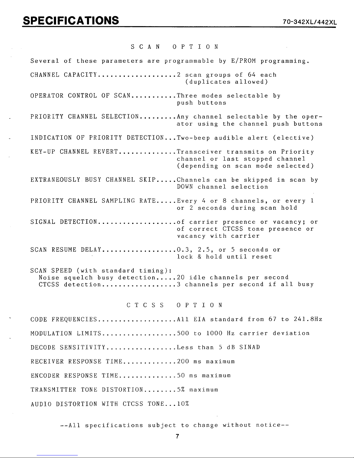
SCAN OPTION
Several of these parameters
are
programmable by E/PROM programming.
CHANNEL CAPACITY
OPERATOR CONTROL OF SCAN
PRIORITY CHANNEL SELECTION Any channel selectable by the oper-
INDICATION OF PRIORITY DETECTION
KEY-UP CHANNEL REVERT
EXTRANEOUSLY BUSY CHANNEL SKIP
PRIORITY CHANNEL SAMPLING RATE
SIGNAL DETECTION
...................
...........
.........
...
..............
.....
.....
...................
2 scan groups of 64 each
(duplicates allowed)
Three modes selectable by
push buttons
ator using the channel push buttons
Two-beep audible alert (elective)
Transceiver transmits on Priority
channel or
(depending on scan mode selected)
Channels can be skipped in scan by
DOWN
Every 4 or 8 channels, or every
or 2 seconds during scan hold
of carrier presence or vacancy; or
of correct CTCSS tone presence or
vacancy with
channel selection
last stopped channel
1
carrier
SCAN RESUME DELAY
SCAN SPEED (with standard timing):
Noise squelch busy detection 20 idle channels per second
CTCSS detection
CODE FREQUENCIES
MODULATION LIMITS 500 to 1000
DECODE SENSITIVITY
RECEIVER RESPONSE TIME
ENCODER RESPONSE TIME 50
TRANSMITTER TONE DISTORTION
AUDIO
DISTORTION WITH CTCSS TONE
..................
.....
..................
CTCSS OPTION
...................
..................
.................
.............
..............
........
...
0.3, 2.5, or 5 seconds or
lock
3
All
Less than 5 dB SINAD
200
5%
10%
&
hold until
channels per second if all busy
EIA standard from
Hz
ms
maximum
ms
maximum
maximum
reset
67
carrier
to 241.8Hz
deviation
--All
specifications subject. to change without notice--
7
Page 10

Page 11
E/PROM PROGRAMMING
The 70-342XL and 70-442XL transceivers contain an Erasable/Program-
mable Read Only Memory (E/PROM) module. The module holds specific
customer frequencies, feature selections, and other parameters that
determine radio operation.
Before final alignment and check, the module must be reprogrammed with
customer specifics. If any option add-on kits are to be installed,
appropriate parameters may also need to be programmed as instructed in
respective kit installation literature.
To change ElPROM electronic information, the plug-in module must first
be erased by exposing it to ultraviolet light using the MIDLAND 701100/1101 ElPROM Eraser. Then, reprogramming is necessary using the
MIDLAND 70-1000 ElPROM Programmer. Operation parameter information is
entered into the Programmer through its keypad, converted into binary
data useful to the transceiver, then written into the E/PROM.
The following are programmable operation parameters in the SYN-TECH
mobile transceivers. See the 70-1000 E/PROM Programmer Operator's
Manual (No. 70-999113) for details.
1.
All eighty transmit and eighty receive channel frequencies
2.
All standard CTCSS tones for each TX and RX channel (requires
installation of the CTCSS module within the transceiver)
3. Time-out-timer time (maximum continuous transmission
duration)
4.
Scan parameters as follows:
a. Two scan groups, each containing up to sixty-four
channels
A
b.
c. Either presence or absence of carrier or correct CTCSS
d. Channel sampling rate (time spent looking for carrier
e. CTCSS decode time (time allotted for decoding after
f. Scan hold time (delay of scan resume after channel
g. Post-transmit scan hold time (delay of scan resume
h. Retention of scan list channels deleted (skipped) by
5.
Busy channel lockout with or without alert tone to the
operator. Adding jumpers allows busy channel inhibit by
CTCSS tone status. See "BCLO JUMPERING".
6.
Transmit-to-receive changeover delay of up to 200ms for
special options.
7. Last selected channel recall on power-up may be disabled.
variety of priority/scan channel revert arrangements
utilizing the two channel lists.
tone to indicate a busy channel
presence on each channel)
carrier is detected)
clears)
after PTT release)
operator activation of the DOWN selector while in scan
mode. Normally, these selections are erased by release
of the SCAN and PRI push buttons and power-down. Programming limits erasure to power-down only.
70-342https://manualmachine.com/442~~
Page 12
H1 VERSION UPGRADE
The E/PROM programmer, model 70-1000, must contain H1 or later version
software to program all features and parameters into the 2-273 E/PROM
modules that are used in the 70-342XL and 70-442XL transceivers. The
version level of software installed in the programmer is identified
for one second in the two far right digits displayed after power-up.
If your programmer contains software that,is older (lower letter) than
the H1 version, upgrade is required. To date of this printing, the
newer L3 version software is current and available (in its own E/PROM)
in Update Kit No. 70-1411. The 70-1000 Operator's Manual also has
been rewritten. The May, 1985 printing can be ordered as MIDLAND part
number 70-999113.
CDCSS OPTION
If the Continuous Digital Coded Squelch System option is installed in
the transceiver, the ElPROM Module is different. This Module, MIDLAND
number 70-2402, is larger in size to accommodate an additional receptacle for connection to the CDCSS board. When programming, the ElPROM
type selection entered into the Programmer is the same as for the
standard EIPROM.
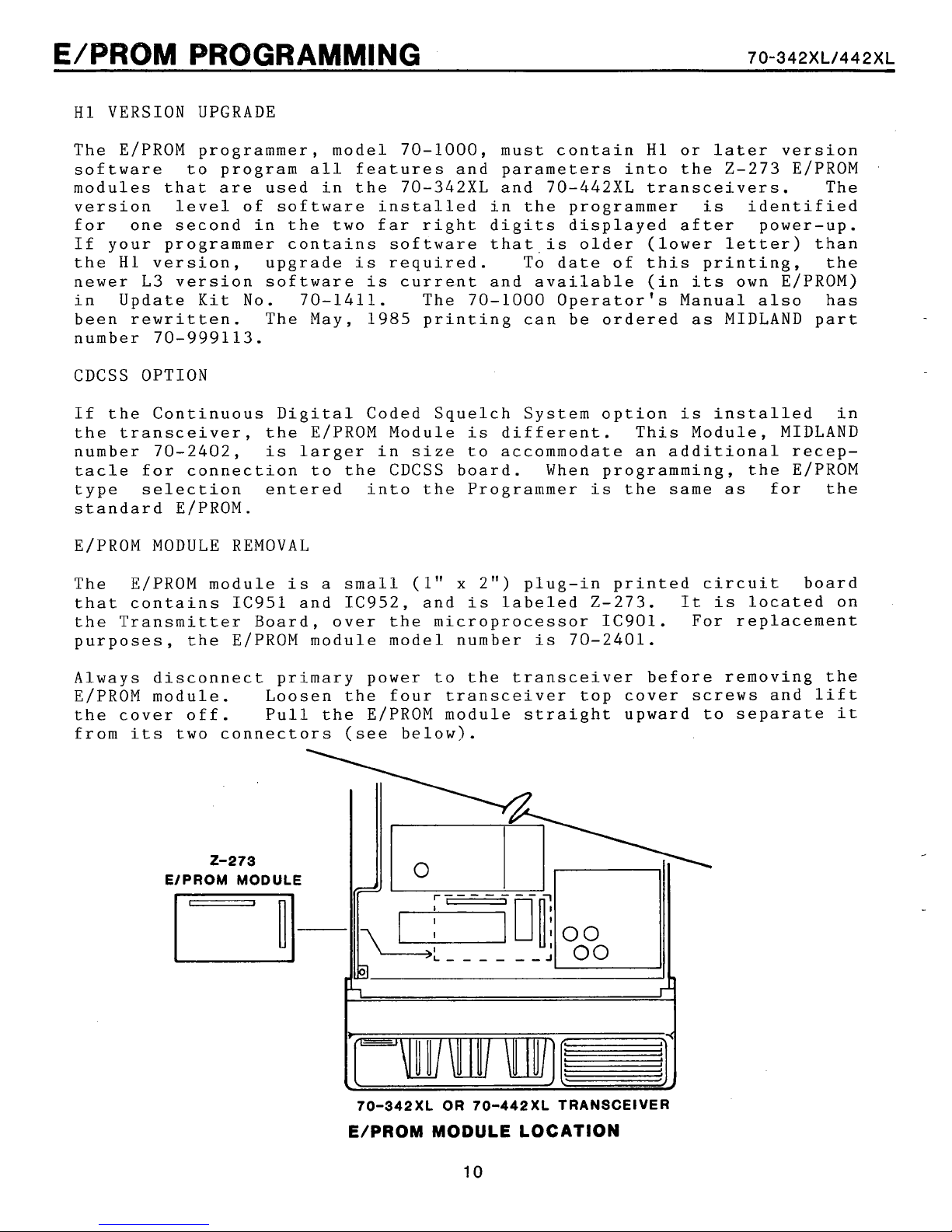
ElPROM MODULE REMOVAL
The E/PROM module is a small (1"
x
2") plug-in printed circuit board
that contains IC951 and IC952, and is labeled 2-273. It is located on
the Transmitter Board, over the microprocessor IC901. For replacement
purposes, the ElPROM module model number is 70-2401.
Always disconnect primary power to the transceiver before removing the
E/PROM module. Loosen the four transceiver top cover screws and lift
the cover off. Pull the E/PROM module straight upward to separate it
from its two connectors (see below).
70-342XL
OR
70-442XL
TRANSCEIVER
E/PROM MODULE LOCATION
Page 13
E/PROM PROGRAMMING
PROGRAMMING
The following E/PROM programming procedure covers most programming for
transceiver operation. Certain infrequently modified parameters are
as
excluded (parameters listed
programming procedures can be found in the Programmer Operator's
Manual.
Heed this precaution:
Do not apply or remove AC-line power to the Programmer while an
E/PROM module
able, to plug the module onto the Programmer until all parameter
information
ready for the BLANK-WRITE-VERIFY operation (step 25).
is
plugged into
is
keystroke entered. Connect the module only when
4h, 6, and 7 on page nine). Complete
it.
It
is
not necessary, nor advis-
70-342https://manualmachine.com/442~~
1.
2. Turn the 70-1000 Programmer on. One of these self-test messages
3.
Erase the E/PROM module in the 70-1100/1101 Eraser. Assure the
E/PROM window
Refer to the Eraser instruction manuax for details.
must appear in the FREQUENCY display for one second: "PASSOL3",
"PASSlL3", "PASSOHll', or "PASSIHll'. The
the required software revision level
programmer. After two seconds, "TYP" should appear in the BAND
display. If an earlier version software
VERSION UPGRADE preceding.
Enter the heading (not necessary for transceiver operation, but
recommended for organization) by pressing [MANUAL], then [ENTER],
then the following:
a. The second part of the transceiver model number ('342A1,
for example). Then [ENTER].
b. Transceiver eight digit
Then [ENTER].
c.
First three digits of a ten digit customer number
(ex.: '123'). Then [ENTER].
d. The last seven digits of the customer number
(ex.: '9ABCDEF1). Then [ENTER].
e.
The month numerically (ex.: March = '3'). Then [/I.
f. The date ('1' through '31'). Then [/I.
g. The
h. Press [RESET] to close heading sequence.
is
last
clean, and
two digits of the year (ex.: '86'). Then [ENTER].
set
serial
exposure
H1
number (ex.: '12345678').
time
last
or L3
is
for 45 minutes.
two digits indicate
is
installed,
installed in the
see
H1
--E/PROM Type Selection--
4.
Press [l] to
should appear. (If the transceiver contains either Talk-Around
option 70-2815 or 70-2816,
by pressing [7] instead of [I]) Press [ENTER].
select
the standard 2-273 E/PROM Module. "2-273"
select
the Z-273TA E/PROM Module type
Page 14
E/PROM PROGRAMMING
70-342https://manualmachine.com/442~~
5.
--Channel Frequency Programming--
The CHANNEL display indicates the numeric channel designator that
appear in the transceiver display. The STEP display indicates what
entry
If an invalid frequency
quency display
frequency.
6.
Select the VHF band and 2.5 KHz PLL reference code by pressing
[2], then [Dl. "15d" should appear in the BAND display (if the
transceiver has been modified with 70-2178 or 70-2179 High-Side
Injection
[ENTER]. The Programmer should now be ready for channel
frequency entry.
is
to be made for that channel--
"1"
"2"
"3"
"4"
CHANNEL
desired receive frequency for channel
point. Then press [ENTER].
Kits,
=
receive frequency
=
receive CTCSS tone frequency or receive CDCSS code
=
transmit frequency
=
transmit CTCSS tone frequency or transmit CDCSS code
will
"1"
use band code [El instead of [Dl). Press
is
entered in the following steps, the fre-
flash. Press [CLEAR], then reenter the correct
and STEP
"1"
should now be displayed. Key in the
1
including the decimal
will
7. CHANNEL
option
or CDCSS code can be entered as described below.
CTCSS Key in the desired CTCSS tone frequency to be decoded
including the decimal point (only standard EIA frequencies
are
Press [ENTER]. If
coded squelch option
CDCSS Key in the desired three-digit standard decode code
(only EIA standard codes
in the FREQUENCY display. If signal
after digits.
carrier squelch operation
option
The Programmer contains
frequencies and CDCSS codes, any of which each
this mode. Press
again to increment through them one
are
stacked on top of the CTCSS tone
scrolling past the highest CTCSS tone. Press [C] to decrement
through the
displayed, press [ENTER] to program.
"l",
is
valid). The digits
STEP "2", should be displayed. If a coded squelch
installed in the transceiver, the CTCSS tone frequency
will
carrier
is
not installed, enter zero.
A
"-"
will
is
installed, enter zero.
a
table of EIA standard CTCSS tone
[Dl
to
call
lists.
When the desired frequency or code
appear in the FREQUENCY display.
squelch operation
are
valid). The digits
is
inverted, key [A]
appear. Press [ENTER]. If
is
desired or no coded squelch
the CTCSS tone frequencies and
at
a
time.
list,
and should appear when
is
desired or no
will
are
accessible in
The CDCSS codes
is
appear
Page 15
E/PROM PROGRAMMING
70-342https://manualmachine.com/442~~
8.
9. CHANNEL
10. Repeat steps 6 through
--Center Frequency Programming--
To afford wideband capability, the self-tuned 70-342XL and 70-442XL
transceivers switch the operating range of their VCO's when selected
channel frequency crosses
controlled by the microprocessor and must programmed into the E!PROM.
Center Frequency values entered into the E/PROM depend on the transceiver frequency band (A-band or B-band).
CHANNEL
transmit frequency for channel
Then press [ENTER]. If the transmitter
channel
is
equipped with a coded squelch option, key in the desired CTCSS
tone frequency or CDCSS code to be transmitted, or nothing for no
tone/code transmission. Then press [ENTER]. The tone/code table
can be used in this mode also.
channels. Channels may be skipped and left unprogrammed.
Channels can be scrolled and re-accessed using the up and down
arrows.
"l",
1,
"l",
STEP
enter zero.
STEP "4", should be displayed. If the transceiver
"3",
should be displayed. Key in the desired
1
including the decimal point.
is
to be disabled in
10
to program the remaining seventy-nine
a
range-center frequency. This switching
is
11.
12. STEP
13.
--Scan Channel Entry--
14. Channel and tone frequency entry
Scroll backward through the channel
arrow push button. Whenever the
channel
accessed and "CF" appears in the CHANNEL display. Stop on the CF
channel.
Frequency entry. Key in '148.12' if the transceiver
model (136-162 MHz range) or key in '160.92' if the transceiver
is
a
STEP
Frequency entry (STEP 2 and 4 do not apply, therefore do not
appear with the CF channel). Key in '147.20' if the transceiver
is
an A-band model (136-161 MHz range) or '160.00' if the
transceiver
[ENTER].
begin scan channel programming sequence. The display
bgank except for the SCAN indicator.
0
to channel 79, the Center Frequency 'channel'
"1"
will
B-band model (148-174 MHz range). Press [ENTER].
"3"
will
also appear, showing readiness for receive Center
appear, showing readiness for transmit Center
is
a B-band model (148-174 MHz range). Press
list
list
is
complete. Press [SCAN] to
with the appropriate
is
looped backwards from
is
will
is
an A-band
be
There are two
list
the transceiver during scan operation differently, depending on
selection of the PRI and SCAN push buttons and Function Mode
programming. Details of operation are found in both the
transceiver and the Programmer operator's manuals.
can be up t.o 64 channels long. The two
lists
of scan channels available--A and B. Each
lists
are used by
Page 16
E/PROM
PROGRAMMING
70-342https://manualmachine.com/442~~
15. Press [A] to program the
display and the first
the BAND display.
16. Key in the channel number to be scanned first in the
press [ENTER]. While
in the CHANNEL display.
17.
18.
19. When the
After [ENTER]
display)
and press enter. If you make an error, press [CLEAR] and
enter. If the channel entered
frequency entry steps above, the CHANNEL display
indicate the error. Press [CLEAR] and enter
Continue entry of the A scan
several scan sequence spots to cause
To
scroll through the
each sequence designator assignment. The highest designator
63.
in the STEP display and the lowest B
designator (0) should appear in the BAND display. Enter B scan
list
highest
will
A
channels in the
list
is
pressed, the
increment to
list
entry
sequence designator
A
list.
list
it
sequence designator "0"
is
keyed, the channel number
1.
list.
A
list,
is
complete, press [B]. "b" should appear
same
manner as A list
"A"
will
A
list
Key in the second A scan channel
was
press the up and down arrows to
sequence designator (BAND
left blank in the channel
A
channel can be entered in
it
list
is
63.
appear in the STEP
will
will
a
valid channel.
to be sampled more often.
scan sequence
entry. Again, the
appear in
A
list,
will
flash to
appear
re-
then
see
is
2C. Press [RESET] to exit the scan programming mode. The Channel
frequency entry mode
"l",
The Busy Channel Lockout feature, Time-Out-Timer feature, and scan
feature parameters
these eight parameters need programming for most applications, therefore attention
program the others (timing adjustments, etc.) can be found in the
Programmer Operator's Manual.
21. BCLO Press [FUNC.] then [ENTER]. "FnC"
display and
programming the Busy Channel Lockout (BCLO) feature,
active. Key in one of the following values, then press [ENTER].
If no entry
value of
for jumper considerations.
and the appropriate frequency.
are
is
given to only these four hereinafter. Procedures to
"1"
in the STEP display. Function Code
is
made, the transceiver
3
--no BCLO. Also
will
programmed in the Function Mode. Only four of
resume displaying CHANNEL
will
will
see
"BCLO JUMPERING'' in this section
operate per the default
appear in the BAND
"OM,
1,
for
is
now
STEP
Page 17
E/PROM
21. continued...
BCLO parameters:
Throughout Function Mode programming, the up and down arrows will
sequentially select the Function Codes.
22. Time-Out-Timer "FnC" and "2" will be displayed. Key in the
parameter value
below, then press [ENTER]. When the transmitter is continuously
keyed for the programmed duration, the timer disables the
transmitter and applies an audible alert tone to the speaker.
The
default value of
inoperative.
PROGRAMMING
O= BCLO without alert. No audible indicating tone will be
heard.
2= BCLO with alert. When the PTT button is pressed while ths
transceiver is inhibited, a tone will be applied to the
speaker.
3= BCLO disabled. No transmit inhibiting per receive status.
to set the Time-Out-Timer duration as listed
timer is reset upon PTT release. If no entry is made, the
0
will be automatic, leaving the Time-Out-Timer
70-342https://manualmachine.com/442~~
O= Disable the Time-Out-Timer
1= 30 seconds
2=
60
seconds
90
3=
23. Press the up arrow four times to skip to Function Code 7.
Function Codes 3 through
their default values.
scan timing, refer to the Programmer Operator's Manual for
procedure.
24. Priority Monitoring '!FnC1' and "7" should be displayed.
Entering a value in this mode either disables priority channel
(see
function is not programmed, the default is one Priority channel
sampling every eight channels scanned, and one Priority sampling
every second when scan is stopped on an active non-priority
channel.
Key in a value listed below, then [ENTER], to program the desired
sampling rates.
erato tor's
O=
1=
2= Sample the Priority channel once every four non-priority
3=
4=
seconds 7= 210 seconds
6
will automatically be programmed with
If
a special application requires altering
manual) sampling or changes its rate.
Sample the Priority channel once every four non-priority
channels scanned, and sample it every second when scan is
stopped.
Sample the Priority channel once every eight non-priority
channels scanned, and sample it every second when scan is
stopped.
channels scanned, and sample it every two seconds when
scan is stopped.
Sample the Priority channel once every eight non-priority
channels scanned, and sample it every two seconds when
scan is stopped.
Disable Priority monitoring
4=
120 seconds
5=
150 seconds
6=
180 seconds
If
this
Page 18
25.
Scan Format "FnC1' and
feature operates in three different mode formats--'Normal1,
'Modified', and 'Secondary'. Each
Manual.
"8"
should be displayed. The scan
is
described in the Operator's
While operating, scan
Programming can
CTCSS detection, absence of detected
correct CTCSS tone with
used in in special applications.
The parameter value determines both scan format and scan stop
aspects
[ENTER]. The default value if no entry
correct whether a coded squelch feature
transceiver or not. If no CTCSS frequency nor CDCSS code
programmed to a channel (steps 6-11), any odd value parameter
programmed
(ex.: If
will
Function Code
*
*
*
*.7=
$5
*
as
listed below. Key in the desired value and press
will
1
is
subtract 1 and operate per parameter 0.).
O=
'NORMAL' Scan Mode with scan stopped by carrier presence
1=
'NORMAL' Scan Mode with scan stopped by presence of
correct CTCSS tone or CDCSS code
2=
'NORMAL' Scan Mode with scan stopped by absence of
3=
'NORMAL' Scan Mode with scan stopped by presence of
without correct CTCSS tone or CDCSS code
4=
'MODIFIED' Scan Mode with scan stopped by
5=
'MODIFIED' Scan Mode with scan stopped by presence of
correct CTCSS tone or CDCSS code
6= 'MODIFIED' Scan Mode with scan stopped by absence of
carrier
'MODIFIED' Scan Mode with scan stopped by presence of
carrier
8=
'SECONDARY' Scan Mode with scan stopped by
9=
'SECONDARY' Scan Mode with scan stopped by presence of
correct CTCSS tone or CDCSS code
A=
'SECONDARY' Scan Mode with scan stopped by absence of
ca'rrier
b= 'SECONDARY' Scan Mode with scan stopped by presence of
carrier without correct CTCSS tone or CDCSS code
set
be decreased by one when read by the transceiver
programmed and CTCSS
8
--
is
stopped by detection of received signal.
scan-stop by noise squelch carrier detection,
carrier
carrier,
presence. The
is
is
is
disabled, the transceiver
or absence of
latter
made
installed in the
is
1,
two
are
which
is
carrier
is
carrier
carrier
without correct CTCSS tone or CDCSS code
carrier
presence
presence
,.
*
:
If the selected channel does not have a CTCSS tone or CDCSS
code programmed to
decrease this parameter value by one and operate accordingly.
26.
Parameter entry
feature
feature
the Programmer Operator's Manual for programming procedures.
This concludes the Function Mode programming sequence. Press
[RESET] to exit.
is
complete. If the last selected channel recall
is
to be disabled, or the operator-deleted scan channel recall
is
to be disabled, or scan timing needs modification; refer to
it,
the transceiver microprocessor
will
Page 19
E/PROM PROGRAMMING
70-342https://manualmachine.com/442~~
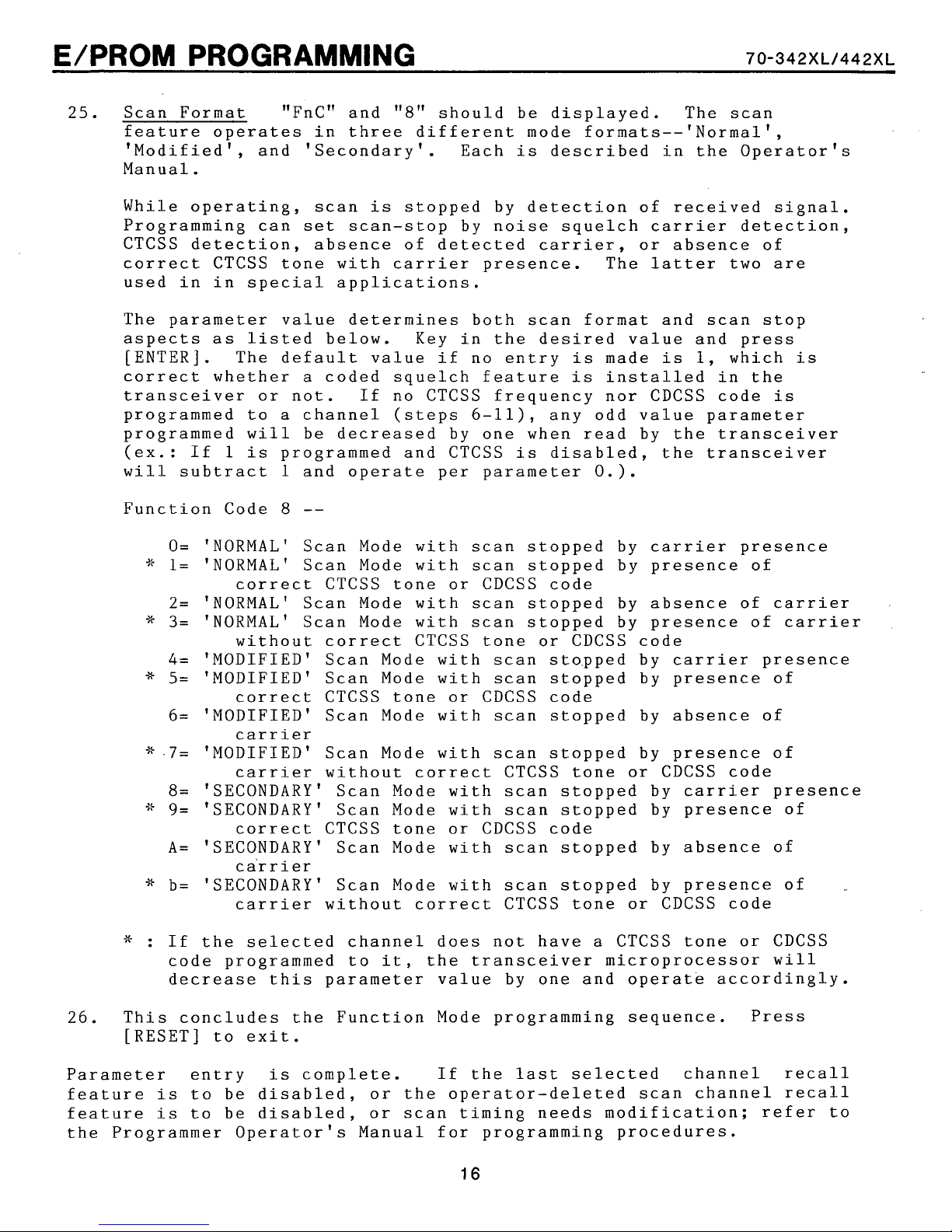
27. Plug the erased 2-273 ElPROM module onto the 70-1000 Programmer
as shown in Figure
2.
2-273
MODE
EIPROM PROGRAMMER
PROGRAMING
EIPROM MODULE
THE
E/PROM MODULE
28. Press [FUNC.] key, then the [4/B.W.V.] key. The BLANK, WRITE,
and VERIFY indicators
module
is
programmed. "PASS"
tent in the E/PROM
will
is
correct. If the readout displays flashing
each illuminate in succession as the
will
be displayed if the new con-
numbers or "ERR", the E/PROM must be erased again, and validity
of the previously entered channel information
is
in question.
29.
Install the E/PROM Module into the transceiver.
BCLO JUMPERING
The Busy Channel Lock-out feature, if programmed as previously described, prevents transmission on
audible
alert
when an attempt
is
a
busy channel and can provide an
made. The standard transceiver
is
configured for BCLO by carrier detection when enabled by programming.
Therefore if neither CTCSS nor CDCSS are used, no jumpers change
necessary. If desired, and if CTCSS (or CDCSS)
transceiver,
a
jumper can be moved to an alternate location inside the
is
installed in the
is
transceiver to prevent transmission only when an appropriate CTCSS
tone
is
received.
The BCLO jumper positions, JP107 and JP108, are located on the Transmitter Board between the modulator (L101, L102) shield and front PC
board edge. Remove the jumper
it
into the JP108 position to
set
wire
from JP107 position and install
BCLO by CTCSS tone (or CDCSS code)
detection. Do not install jumpers in both positions.
Page 20
TRANSCEIVER CALIBRATION
70-342https://manualmachine.com/442~~
SUGGESTED TEST EQUIPMENT FOR TRANSMITTER CALIBRATION
Test Instrument Instrument Capabilities Instrument Type
DC Power Supply 13.8 VDC, 10 amps Power Mate BPA-20PF
Wattmeter
50 watts, 136-174 MHz Bird model 43 with 50C
element and 50 ohm load
Deviation Meter 136-174 MHz.
p/o Cushman CE-31A
+/-5KHz range
Frequency Meter or 136-174 MHz p/o Cushman CE-31A or.
Frequency Counter 2.0 ppm accuracy Heath SM-4120
Audio Generator 0-10 KHz sine-wave, Heath SG-5218
0-5 Vrms output
POWER
CALIBRATION
SUPPLY
SET-UP
Page 21
TRANSCEIVER CALIBRATION
The 70-342XL and 70-442XL wideband transceivers are capable of opera-
ting across
realignment
frequencies. Only transmit carrier calibration such as frequency,
modulation, and output power may need adjustment. The transceivers
are shipped from the factory programmed with test frequencies that
must be changed to customer frequencies before installation.
REALIGNMENT
sceiver tuning has been replaced. Realignment requires transceiver
operation on special frequencies, therefore they must be programmed
into the transceiver E/PROM specifically for alignment. The complete
Alignment procedure can be found in the SERVICING SECTION of this
manual.
a
24
MHz channel frequency spread. Therefore, receiver
is
not needed, even when reprogrammed with new customer
MAY
BE NECESSARY ONLY AFTER a component that affects tran-
-
70-342https://manualmachine.com/442~~
Error code 90, 91, 92, 93, or 94 appearing in the channel display with
-
continuous triple-beeps indicates the E/PROM module
improperly inserted, or incorrectly programmed. Check the E/PROM
module or refer to the E/PROM Programming section in this service
manual.
Error code 95 appearing in the channel display with
indicates the synthesizer phase-lock-loop cannot achieve lock.
defect exists and
it
must be corrected.
is
missing,
a
triple-beep
A
Page 22
TRANSCEIVER CALIBRATION
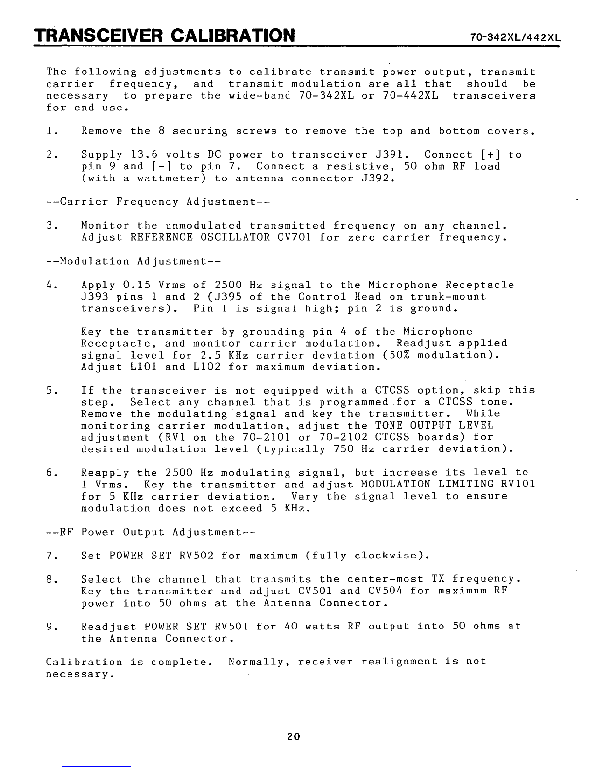
The following adjustments to calibrate transmit power output, transmit
carrier frequency, and transmit modulation are all that should be
necessary to prepare the wide-band 70-342XL or 70-442XL transceivers
for end use.
8
1. Remove the
securing screws to remove the top and bottom covers.
70-342https://manualmachine.com/442~~
2.
--Carrier Frequency Adjustment--
3. Monitor the unmodulated transmitted frequency on any channel.
4.
5.
Supply 13.6 volts DC power to transceiver 5391. Connect
9
and
[-I
pin
(with a wattmeter) to antenna connector 5392.
Adjust REFERENCE OSCILLATOR CV701 for zero carrier frequency.
Apply 0.15 Vrms of 2500 Hz signal to the Microphone Receptacle
5393 pins 1 and 2 (5395 of the Control Head on trunk-mount
transceivers). Pin 1 is signal high; pin 2 is ground.
Key the transmitter by grounding pin
Receptacle, and monitor carrier modulation. Readjust applied
signal level for 2.5 KHz carrier deviation (50% modulation).
Adjust LlOl and L102 for maximum deviation.
If the transceiver is not equipped with a CTCSS option, skip this
step. Select any channel that is programmed.for a CTCSS tone.
Remove the modulating signal and key the transmitter. While
monitoring carrier modulation, adjust the TONE OUTPUT LEVEL
adjustment (RV1 on the 70-2101 or 70-2102 CTCSS boards) for
desired modulation level (typically 750 Hz carrier deviation).
to pin 7. Connect a resistive, 50 ohm RE load
4
of the Microphone
[+]
to
6.
--RE Power Output Adjustment--
7.
8.
9.
Calibration is complete. Normally, receiver realignment is not
necessary.
Reapply the 2500
1 Vrms. Key the transmitter and adjust MODULATION LIMITING RVlOl
5
for
modulation does not exceed
Set POWER SET RV502 for maximum (fully clockwise).
Select the channel that transmits the center-most TX frequency.
Key the transmitter and adjust CV501 and CV504 for maximum RE
power into 50 ohms at the Antenna Connector.
Readjust POWER SET RV501 for
the Antenna Connector.
KHz carrier deviation. Vary the signal level to ensure
Hz
modulating signal, but increase its level to
KHz.
5
40
watts RF output into 50 ohms at
Page 23
TRANSCEIVER CALIBRATION
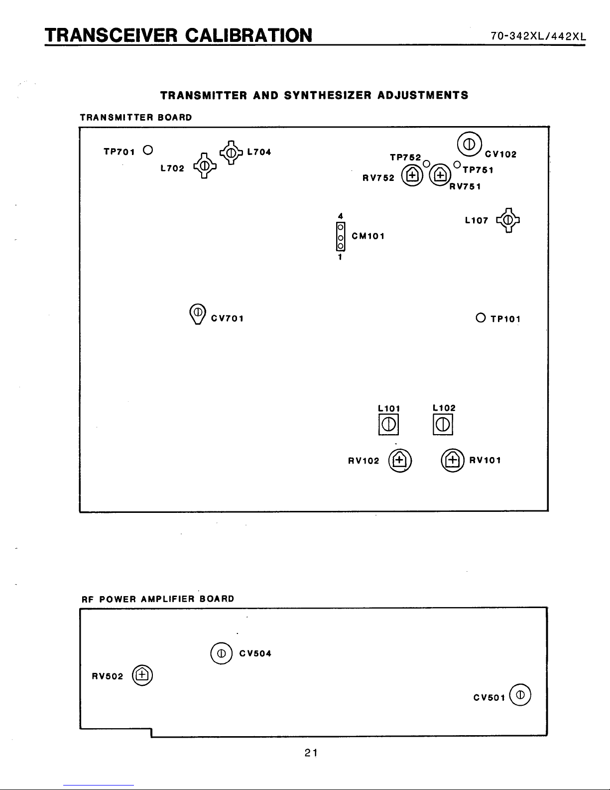
TRANSMITTER AND SYNTHESIZER ADJUSTMENTS
TRANSMITTER BOARD
70-342https://manualmachine.com/442~~
RF POWER AMPLIFIER BOARD
Page 24
UNDER-DASH MOUNTING (Model 70-342XL only)
The 70-342XL transceiver
is
designed for use in automobiles, trucks,
or other vehicles with 12 volt electrical systems. Where in the
vehicle the transceiver
provided
its
front panel controls
mounted does not affect
are
accessible to the operator.
its
performance,
is
Typical mounting locations are under the dashboard or next to the
driver's
The transceiver
seat.
is
housed in
a
slim,
small
package to best conform to
mounting locations. The mounting bracket slides into the transceiver
a
siderails and provides
3.25 x 7.75 inch flat surface across the
transceiver top with holes for bolting to a flat surface in the vehi-
cle.
the four
5/32" holes must be drilled in the mounting surface to accept
3/8"
screws and washers provided.
TRUNK MOUNTING (Model 70-442XL only)
is
The 70-442XL trunk mount transceiver
such
a
ceiver
design,
as
a
vehicle trunk or under a seat. The operator controls
compact control head for operator access. The bulk of the trans-
is
within the separate remotely mounted unit. Because of this
its
does not have an internal speaker. Instead,
designed for remote mounting
are
in
a
separate
3.2-ohm external speaker (included with the 70-442XL package) nust be
installed and connected to the Control Head.
The cable that interconnects the control head to the trunk unit
is
four meters long and flat for laying under carpeting. The cable must
not lay near hot areas (above the catalytic converter, for example)
nor against sharp edges.
A
trunk unit mounting tray
is
flat tray
the trunk unit
7.5 inches square and must be bolted to the surface where
will
mount. 5/32" holes must be drilled in the mount-
ing surface to accept the four
13
x 8 x 3 inch trunk unit then clips onto the tray.
A
Control Head mounting bracket.
Its
surface
is
314 inch wide and 4 inches long with two screw holes
is
provided with each transceiver. The
3/8"
screws and washers provided. The
is
provided with each transceiver.
2
inches apart. 5/32" holes must be drilled in the mounting surface of
the vehicle to accept the the
318"
Control Head and bracket assembly
wide, and
3
112 inches deep.
At
screws and washers provided. The
is
2 112 inches high, 4 114 inches
least
314 inch of additional depth
is
needed for the connectors that attach to the rear of the Control Head.
REMOTE SPEAKER (required and included with the 70-442XL)
As
part of the standard trunk-mount transceiver configuration (model
70-442XL), the model 70-2353 5-watt speaker connects to the Control
Head Accessory Plug.
It
also can be used optionally with the 70-342XL
under-dash transceiver to substitute the transceiver internal speaker.
Its
5
112 ft. cable
is
terminated with appropriate Molex pins for
Page 25
1
INSTALLATION
insertion into the trunk-mount Accessory Plug on the Control Head or
the under-dash Power/Accessory Plug. The speaker housing and mounting
bracket assembly
is
surface
4 1/4 x 1 114 inches, with four 3/32"
POWER REQUIREMENTS
Both the 70-342XL and 70-442XL transcqivers are designed to operate
a
from
12 volt DC, negative ground, automotive
Current drain of
of the vehicle
other
electrical
CAUTION: CHECK THE VOLTAGE SOURCE BEFORE CONNECTING THE POWER CABLE.
TOO MUCH VOLTAGE (ABOVE
70-342https://manualmachine.com/442~~
is
5x5 inches square by 3 inches deep. The mounting
at
least 10 amperes should be expected. Inspection
is
recommended prior to installation.
screw
slots.
electrical
A
low battery or
system.
system defects may degrade transceiver performance.
16
VOLTS) CAN SEVERELY DAMAGE THE TRANSCEIVER.
Included with the trunk-mount transceiver
The under-dash transceiver
is
shipped with a 2
is
a
6
meter
meter
DC power cable.
Power/Accessory
cable. Each cable includes fused power leads for connection to vehi-
cle
to the negative
GROUND VEHICLE. If the transceiver
electrical
system. Because the transceiver chassis
(-)
lead,
DO
NOT INSTALL THE TRANSCEIVER
is
used as a base station, the
is
connected
IN
A
POSITIVE
external AC-line-to-DC power supply must be adequately regulated and
have sufficient current capacity.
ANTENNA
The most important communications system component that can affect
overall performance
to provide 50 ohm terminating impedance
frequencies
follow
its
is
manufacturer's instructions.
is
the antenna.
A
good quality antenna designed
at
appropriate transceiver
recommended. When adjusting the antenna, be sure to
A
better quality SWR
meter
should be used to accurately measure minimum reflected energy.
MICROPHONE HANGER
The hand microphone included with the transceiver has
backside to
three
screws
screws and three 314"
mate
with
its
hang-up clip. The clip must be mounted with
in a location convenient to the operator. Three 1/2"
screws,
each requiring a 5/64" hole,
button on
are
its
also
a
provided.
An optional microphone hanger (model 70-2195)
with the CTCSS option. This hang-up box may be installed in place of
the microphone clip on both
screws
provided. Wiring instructions fol3.o~ in the Power/Accessory
Plug instructions.
metallic
is
available for use
or non-metallic surfaces with two
Page 26
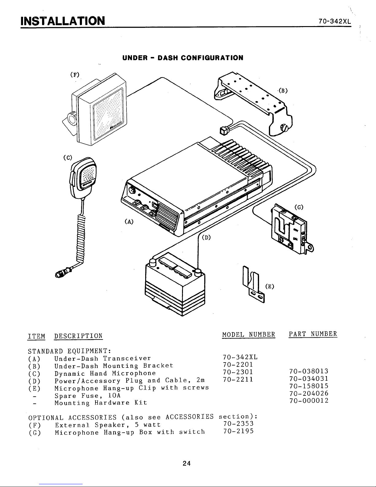
INSTALLATION
70-342~~
UNDER - DASH CONFIGURATION
ITEM DESCRIPTION
STANDARD EQUIPMENT:
(A)
(B)
(C) Dynamic Hand Microphone
(D)
(E)
-
-
OPTIONAL ACCESSORIES (also see ACCESSORIES
(F)
(G)
Under-Dash Transceiver
Under-Dash Mounting Bracket
Power/Accessory Plug and Cable, 2m
Microphone Hang-up Clip with screws
Spare Fuse, 10A
Mounting Hardware Kit
External Speaker, 5 watt
Microphone Hang-up Box with switch
MODEL NUMBER PART NUMBER
section)
70-2353
70-2195
:
Page 27
lhlSTALLATlON
70-442XL
TRUNK - MOUNT CONFIGURATION
ITEM DESCRIPTION MODEL NUMBER PART NUMBER
STANDARD EQUIPMENT:
(A) Trunk-Mount Transceiver 70-442XL
(B) Trunk-Mount Mounting.Bracket 70-2206
(C)
(D) Accessory Plug 70-2222
(E)
(F)
(G)
(I)
(I)
-
-
OPTIONAL ACCESSORY (also
(J)
Dynamic Hand Microphone 70-2301
Control Head Mounting Bracket
Microphone Hang-up Clip with
Speaker,
Trunk Mounting Tray, with keys 70-2205
Power Plug and Calde, 6m 70-2212
Spare Fuse,
Mounr ing Hardware
Microphone Hang-up Box with switch 70-2195
5
watt
LOA
Kit
see
ACCESSORIES section):
screws
70-2353
25
Page 28
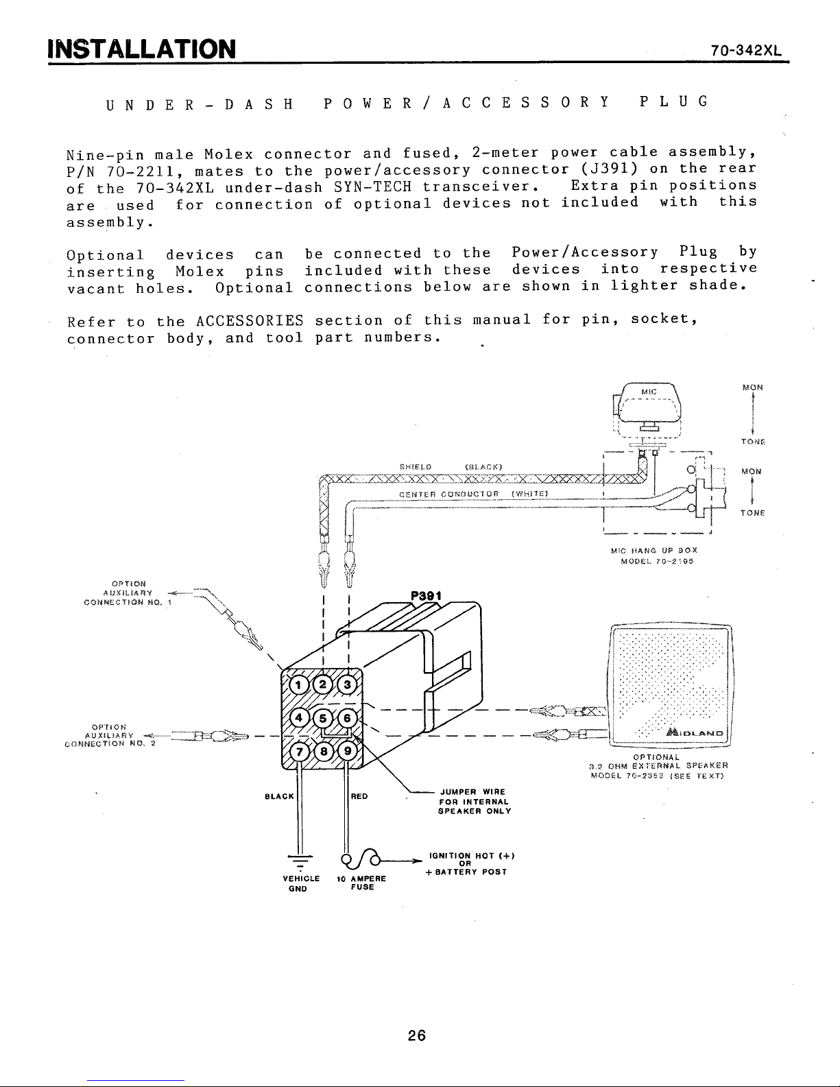
UNDER-DASH POWER/ACCESSORY
PLUG
Nine-pin male Molex connector and fused, 2-meter power cable assembly,
P/N 70-2211, mates to the power/accessory connector (5391) on the rear
of the 70-342XL under-dash SYN-TECH transceiver. Extra pin positions
are used for connection of optional devices not included with this
assembly.
Optional devices can be connected to the Power/Accessory Plug by
inserting Molex pins included with these devices into respective
vacant holes. Optional connections below are shown in lighter shade.
Refer to the ACCESSORIES section of this manual for pin, socket,
connector body, and tool part numbers.
MUM
1
TONE
MON
0
I
TONS
OPTZOW
bU)III.IARY
COHP4ECTIQN
OP'I
10
H
BUXILJhAY
MMEGTIOH
NU.
MO.
*.+.-
2
Page 29
lNSTALLAVlON
UNDER-DASH POWER CONNECTIONS
The Power/Accessory Cable
connection to the vehicle
are
2
meters
and chassis ground.
long; sufficient for typical connection to a fuse block
is
equipped with two 14 gauge
electrical
system. The unterminated
wires
70-342XL
for
wires
Connect the black
vehicle--DO NOT ATTEMPT TO INSTALL THE TRANSCEIVER
GROUND VEHICLE.
body or chassis often provides an adequate ground if
secure the
Connect the red
electrical system. Because of current requirements, connection to an
existing fused circuit should be avoided to prevent overload of that
fuse. This
penetration and transceiver defect. The connection can be made to
Ignition HOT to switch the transceiver with ignition, or to Battery
HOT to enable the last-selected-channel feature of the transceiver.
In the
Either connection
the red transceiver
EXTERNAL SPEAKER (Models 70-2352, and 70-2353):
Normally, the transceiver internal speaker
ceive audio by the jumper to pins 5 and 6. If one of the MIDLAND
external speakers
to disable the internal speaker and the two wires from the external speaker must connect to pins
Power Speaker
tor (white) must be connected to pin 6, and the shield (black) to
pin
wire
wire
latter
4.
to
wire
case,
wire
A
large bolt that
it.
to the positive
has
is
wire
UNDER-DASH OPTIONAL CONNECTIONS
is
to the negative
screws
(+),
its
own in-line fuse for protection against
the transceiver must be turned off separately.
usually available in the vehicle fuse block ,if
is
terminated with an appropriate lug.
is
to be utilized, the jumper must be removed
4
to be connected,
(-)
chassis ground of the
IN
A
POSITIVE
into the
or Hot side of the vehicle
and
6.
its
input cable center conduc-
metallic
a
lug
is
connected to
NOTE: If the 70-2352
vehicle
is
used to
wire
re-
HANG-UP BOX (Model 70-2195):
If the CTCSS feature
70-2195 Microphone Hang-up contact/switch-box usually
led to unmute CTCSS squelch when the microphone
center conductor of the shielded hang-up box cable connects to
3,
pin
option board within the transceiver must also be removed.
AUXILIARY DEVICES:
Pins
with certain opticnal features. Wiring details for these
found in the respective literature for the option.
the shield to pin 2. Jumper JP2 on the 70-21028 CTCSS
1
and 8 are available for auxiliary connections necessary
is
included in the transceiver, the optional
is
instal-
is
lifted. The
are
Page 30
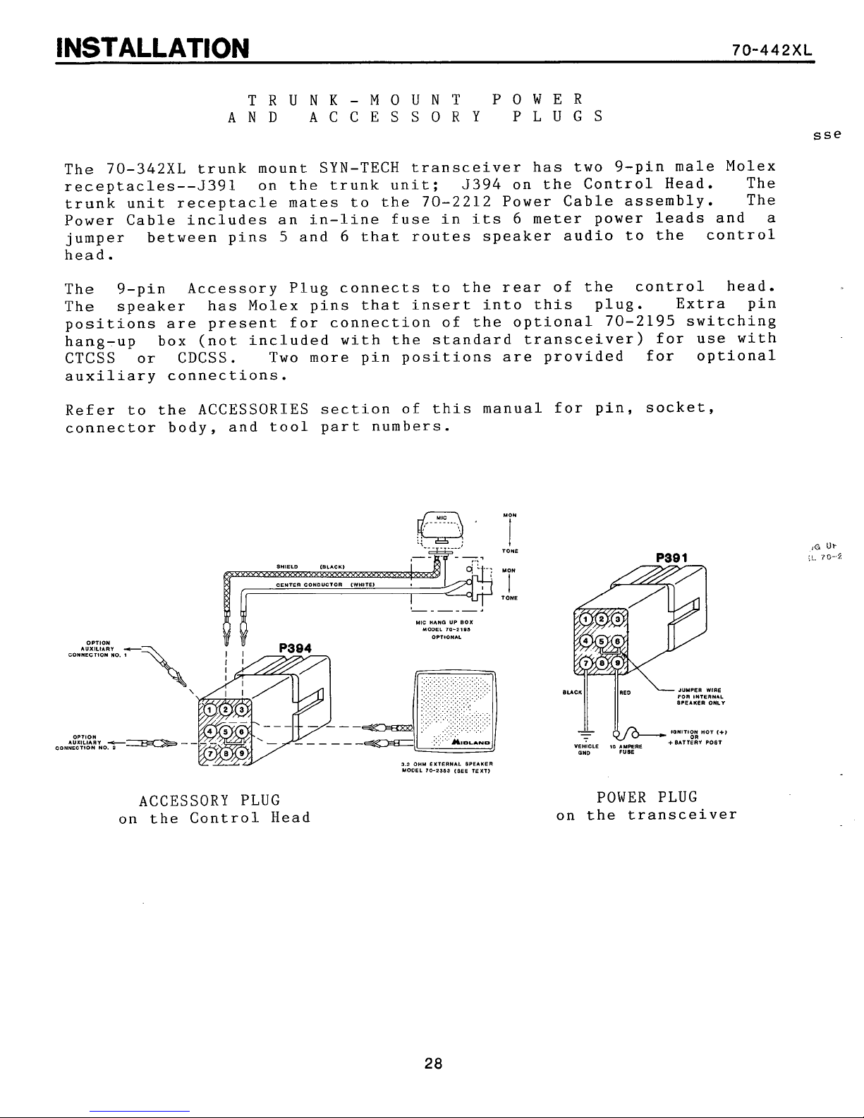
TRUNK-MOUNT POWER
AND
ACCESSORY PLUGS
The 70-342XL trunk mount SYN-TECH transceiver has two 9-pin male Molex
receptacles--J391 on the trunk unit; 5394 on the Control Head. The
trunk unit receptacle mates to the 70-2212 Power Cable assembly. The
Power Cable includes an in-line fuse in
its
6
meter power leads and
a
jumper between pins 5 and 6 that routes speaker audio to the control
head.
The 9-pin Accessory Plug connects to the rear of the control head.
The speaker has Molex pins that insert into this plug. Extra pin
positions
are
present for connection of the optional 70-2195 switching
hang-up box (not included with the standard transceiver) for use with
CTCSS or CDCSS. Two more pin positions are provided for optional
auxiliary connections.
Refer to the ACCESSORIES section of this manual for pin, socket,
connector body, and tool part numbers.
OPTION
AUXILIARV
COHllECIlOW NO
OPIlOll
AUXILIARY
CONWECTlOW NO.
C
2
ACCESSORY PLUG
on the Control Head
WIC
HANO UP
UOOEL
5.2
OHM
EXTERNAL
UOOEL
70-2319 (SEE TEXT)
70-2101
BOX
SPEAKER
TONE
'
r
TOHE
I I
8JL-y;::;;;;;)
VEHICLE
10
AMPERE
(1~0 FUME
POWER PLUG
on the transceiver
Page 31

INSTALLATION
TRUNK-MOUNT POWER CABLE CONNECTIONS
The 70-2212 Power Cable
tion to the vehicle
meters
chassis ground.
long; sufficient for typical connection to a fuse block and
is
equipped with two 12
electrical
AWG
wires
system. The unterminated
70-442XL
for connec-
wires
are 6
Connect the black
vehicle--DO NOT ATTEMPT TO INSTALL THE TRANSCEIVER
GROUND
body or chassis often provides an adequate ground.if
secure the
Connect the red
electrical system. Because of current requirements, connection
existing fused circuit should be avoided to prevent overload of that
fuse. This
penetration and transceiver defect. The connection can be made to
Ignition HOT to switch the transceiver with ignition, or to Battery
HOT. The
transceiver, but the transceiver must be turned off separately. Either
connection
transceiver
STANDARD EXTERNAL SPEAKER (Model 70-2353):
VEHICLE.
wire
to
wire
wire
latter
is
usually available in the vehicle fuse block if the red
wire
CONTROL HEAD ACCESSORY PLUG CONNECTIONS
The two
for insertion into positions
mates
wires
to the Control Head.
wire
A
large bolt that
it.
to the positive
has
enables the last-selected-channel feature of the
is
terminated with an appropriate lug.
of 70-2353 speaker are terminated with Molex pins
to the negative
(-)
chassis ground of the
IN
screws
(+),
its
own i-n-line fuse for protection against
4
and 6 of the Accessory Plug that
into the metallic vehicle
a
lug
or Hot side of the vehicle
A
POSITIVE
is
used to
to
wire
an
OPTIONAL 15 WATT POWER SPEAKER (Model 70-2352):
The 70-2352 power speaker has
terminated with Molex pins for inserting into the Accessory Plug.
The center conductor (white) of this audio signal cable must be
connected to pin 6, and the shield (black) to pin
(+)
red
that the transceiver DC power leads are connected.
OPTIONAL HANG-UP BOX (Model 70-2195):
If the CTCSS feature
microphone hang-up contact/switch-box usually
unmute CTCSS squelch when the microphone
conductor of the shielded hang-up box cable connects to pin
the shield to pin 2. Jumper JP2 on the 70-2102A CTCSS option
board within the transceiver must also be removed.
AUXILIARY DEVICES:
Pins
with certain optional features. Wiring details for these are
found in the respective literature for the option.
and black
1
and 8 are available for auxiliary connections necessary
(-)
power leads that connect to the same points
is
included in the transceiver, the 70-2195
a
shielded coaxial cable that
4.
It
also has
is
installed to
is
lifted. The center
is
3,
Page 32

Page 33

AUTOMOTIVE RECEIVER INTERFERENCE
Occasionally, the technician who installs land-mobile radio equipment
-
is
plagued with interference originating somewhere in the automobile
that produces annoying noises through the transceiver. Interference
problems
into the transceiver, locating
it
the simplest way available.
Interference enters the transceiver two ways: by conduction or induction. Conducted interference passes through the DC power leads.
Inductive interference
may be anywhere in the vehicle.
are
solved by understanding the interference and
its
source logically, then eliminating
is
radiated through the
air
from a source that
70-342https://manualmachine.com/442~~
its
path
Conducted interference
electrical
a
vehicle, current surges produce respective voltage drops across
resistances. Thus, voltage transient (switching) spikes appear
throughout the electrical system. Connecting the transceiver power
leads to this noisy
directly to the radio. Although most of the noise voltage
uated by power-line filters within the radio, spikes that
enough may be audible.
While interference conducted through power leads affects transceiver
audio circuitry; inductive interf:erence
quencies, or even channel frequencies, and
receiver. Inductive interference
induces noise currents in the transceiver antenna, accessory cabling,
or chassis (see Figure
A
spark
frequency spectrum; thus,
cally in modern vehicles, sparks
ignition system, and fan motors.
Other common sources of inductive energy
electronic gadgets found in modern vehicles. Their internal oscilla-
tors produce high frequency signals and radiate energy
the signal frequency.
system. With many electrical devices turning on and off in
is a common source of electromagnetic energy across the radio
is
simple noise voltage present in the vehicle
electrical
system applies the noise voltage
is
atten-
are
imitates
is
an electromagnetic field that
receiver
is
demodulated by the
I.F.
1).
a
source of inductive interference. Typi-
are
found in the alternator, the
are
within
a
variety of
at
multiples of
wire
severe
fre-
THE
LOCATING
The first step toward eliminating interference
interference source and path-of-entry into the transceiver. Listening
to the noise can
transceiver varies with engine speed,
the engine; such
Because the transceiver
coupling into the transceiver (by conduction or ind.uct.ion)
With
transceiver that
could be radiated i.nto the receiver. Because conducted interference
all
SOURCE
tell
as
the alternator, ignition system, or tachometer.
squelch circuits open, apply an unmodulated signal to the
is
is
to determine the
a
lot. For example: if the noise heard in the
its
source must be related to
is
an
FM
radio, determining interference
is
easy.
strong enough to overcome any int-erference that
Page 34

AUTOMOTIVE RECEIVER INTERFERENCE
70-342https://manualmachine.com/442~~
can only affect audio circuitry,
is
Another method of testing
the lowest noise point in the vehicle electrical system: the battery.
Because the battery acts like
ducted,
ELIMINATING CONDUCTED NOISE
If there
in the vehicle electrical system that needs repair.
tion of this nature
creates
noticeably impair vehicle operation.
a
whine in the transceiver that varies in pitch with engine speed.
Also, the defective diode causes excessive arcing in the brushes,
which may produce some inductive interference.
Another possible source of conducted interference
Because
path-of-entry
mostly conducted, find
system for the transceiver that
ELIMINATING INDUCTIVE INTERFERENCE FROM NEARBY OSCILLATORS
will
cease.
is
a
conducted noise path, there probably
is
a defective diode in the alternator, which
a
large current ripple at alternator output but may not
a
fan also produces inductive interference, determine which
is
most predominant (see above). If the interference
to connect the power leads directly to
a
power connection point in the electrical
it
will
a
large capacitor, the noise, if con-
is
further from the fan circuit.
still
A
bad alternator diode produces
be heard if present.
is
a
defective
A
common condi-
is
a
fan motor.
item
is
If testing proves interference
of applicable inductive sources--sparks and high frequency oscillators. Modern vehicles utilize many electronic gadgets and systems
that may produce a hash or whine in the transceiver. Oscillators
within these devices, that sometimes are poorly shielded, may radiate
an electromagnetic field at frequencies many multiples of the oscillator frequency.
Again, listen to the noise to learn about
interfering gadget
with engine speed. The interfering gadget can be isolated by temporarily removing power to
Because lead-in
is
ference
gadget itself. If so, check that the wiring to the device
the transceiver or
nected in
device; close to
'sensitive'
movement.
Inductive interference may also enter through the radio receiver
input--the antenna. This can be verified by substituting the antenna
and
dummy load
Without
the noise stops, interference
its
it,
more often radiated from the gadget's wiring than the
series
wires
cable with a matched dummy load and short cable (The 50 ohm
is
the receiver may become less sensitive to any signal). If
is
part of engine operation, the noise won't vary
it
wires
with the 'sensitive' lead-in wires of the interfering
its
may be identified if noise volume changes with wire
necessary to properly balance the receiver input.
act like radiating antennas, inductive inter-
its
wiring. If necessary, RF chokes can be con-
housing to kill the antenna effect. Sometimes,
is
not conducted, there are two types
its
source. Unless the
to check for absence of noise.
is
entering the antenna port.
is
not near
Page 35

AUTOMOTIVE
ELECTROMAGNETIC
RADIATION AT
RECEIVER
RECEIVER
INTERFERENCE
MODERN ELECTRONIC
DEVICE WITH INTERNAL
OSCILLATOR THAT PRODUCES
INDUCTIVE INTERFERENCE
AS RADIATING
70-342https://manualmachine.com/442~~
NOISE VOLTAGE
ACROSS Rw IS
CONDUCTED DIRECTLY
INTO TRANSCEIVER
VOLTAGE PRODUCED
BY
HIGH CURRENT
SURGES THROUGH Rw.
-
-
-
12
CHOKE KILLS
ANTENNA EFFECT
ELECTRICAL
WIRING TO
DEVICE
IGNITION
ALTERNATOR WITH
BAD INTERNAL DIODE
VOLTS
H
SllRCES ARE
SMOOTH ED
BATTERY CAPACITY
FIGURE
ICH CURRENT
BY
1
-
CONDUCTIVE AND INDUCTIVE INTERFERENCE
HIGY CURRENT
SURGES CAIJSED
BY
DEFECTIVE
ALTERNATOR
Page 36

AUTOMOTIVE RECEIVER INTERFERENCE
70-342https://manualmachine.com/442~~
If interference into the antenna originates from
gadget, reduce radiation from the source with RF chokes
above. Sometimes, positioning the antenna further from the gadget may
work.
ELIMINATING INDUCTIVE INTERFERENCE FROM SPARKS
Only a few areas remain in modern vehicles that produce sparks: the
alternator, ignition system, and fan motors. Sparks in modern alternators generally do not produce sufficient inductive interference
is
a
unless there
produce significant conducted interference, too.
Modern vehicles use higher voltage ignition systems.
electrical leakage occurs more easily through cracks and contaminants.
If the interference produces
in pitch with engine speed, and seems to be the same rate
spark, sparks
plug wires. Check the ignition coil,
distributor cap for signs of arcing through cracks and burns or over
dirt.
If the interference produces a popping sound in the transceiver at
engine idle that seems to occur in time with firing of a single spark
plug, and increases in rate with engine speed,
wire
spark plugs for cracks, burns, and dirt.
are
suspect. Check the distributor cap, spark plug
related defect. If so, the defect probably
a
buzz in the transceiver that increases
are
leaking to ground before distribution to the spark-
its
high voltage
a
poorly shielded
as
described
As
a
result,
as
every
wire,
a
single spark plug or
wires,
will
and
and
Spark plug and ignition coil
(resistive) conductors to reduce electromagnetic radiation. Older
vehicles may not be equipped
applicable.
Fan motor interference from
with fan speed. Badly worn brushes or bearings cause excessive
sparks, therefore replacement may be necessary.
capacitor can be connected to the positive lead
as practical to reduce inductive interference. The capacitor body
must connect securely to the grounded motor housing.
as
its
wires
such.
brushes produces a whine that varies
are
Use
made with suppressive
an ohmmeter to verify, if
A
0.1
as
close to the motor
uF coaxial
Page 37

OPTIONAL ACCESSORIES
The followi.ng ark optional mobile installation accessories that are
available from MIDLAND.
CONTROL CABLE ASSEMBLIES
Assemblies of cables terminated with 34-pin female connectors to
connect the SYN-TECH Control Head to trunk unit.
70-342https://manualmachine.com/442~~
Flat ribbon cable, 6 meters long
Flat ribbon cable, 2 meters long
Round cable, 4 meters long
Round cable, 2 meters long
REMOTE SPEAKER (5 Watt) Model No. 70-2353
A
3.2 ohm, housed speaker with mounting bracket and screws to
substitute the 70-342XL internal speaker (the 70-2353 speaker
standard with the 70-442XL transceiver).
terminated with appropriat-e Molex pins for insertion into the
transceiver Power/Accessory Plug. The speaker with
bracket
POWER SPEAKER (15 Watt) Model No. 70-2352
This self-contained amplified speaker
the 70-2353 Remote Speaker.
nated with appropriate Molex pins to connect to the 70-342XL
Power/Accessory Plug or the 70-442XL Accessory Plug.
fused power leads must be connected to vehicle
ALL WEATHER SPEAKER Model No. 70-SO5
A
5
grill.
for insertion into the 70-342XL Power/Accessory Plug or the 70-
442XL Accessory Plug. The speaker
inches deep, and mounts with a swivel tab.
is
watt,
Its
5x5 inches square by 3 inches deep.
Its
5.5 ft. input cable
4 ohm, outdoor speaker that can be mounted in a vehicle
8
ft. cable
is
terminated with appropriate Molex pins
is
Its
is
identically housed as
5
1/2 inches diameter, 4
Model
Model No. 70-2223
Model
Model No. 70-2227
5.5 ft. cable
(+)
No. 70-2221
No. 70-2226
its
mounting
is
termi-
Its
5.5 ft.
and ground.
is
is
MICROPHONE HANG-UP BOX Model No. 70-2195
Detects presence of a microphone in
nel monitoring by defeating CTCSS (or CDCSS) audio squelch. This
accessory
CTCSS (or CDCSS) feature.
has 5.5 ft. cable terminated with appropriate Molex pins for
insertion into the under-dash transceiver Power/Accessory Plug or
the trunk-mount transceiver Accessory Plug.
HANDSET MICROPHONE Model No. 70-2311
A
handset and cradle set with instructions and appropriate Molex
wire terminations to connect to the 70-342XL Power/Accessory Plug
or the 70-442XL Accessory Plug (on the Control Head). Minor
internal wiring alteration
through the connector.
is
useful only if the transceiver
It
is
is
necessary to route audio signals
its
clip for automatic chan-
is
equipped with the
shipped with mounting screws and
Page 38

OPTIONAL ACCESSORIES
70-342https://manualmachine.com/442~~
HAND
HAND
WEATHER-PROOF CONTROL HEAD Model No. 70-2210
MICROPHONE WITH DTMF PAD Model No. 70-2103A
A
hand microphone with built-in lighted four-by-four DTMF keypad
(16 keys;
for signaling and phone-patch
on/off switch and channel up and down
NOTE:
and wired inside the transceiver or Control Head. This receptacle
is
MICROPHONE WITH DTMF PAD
This complete hand microphone
it
also includes circuitry for the automatic number identifier
feature.
NOTE:
and wired inside the transceiver or Control Head. This recepta-
cle
is
A
replacement for the 70-2209 SYN-TECH Control Head (with scan).
It
is
identical in size and shape, but designed for outdoor use.
Shipped with the
0-9,
A
special 6-pin microphone receptacle must be installed
included with the microphone.
A
special 6-pin microphone receptacle must be installed
included with the microphone.
*,
same
#,
and A-D) and encoder to transmit DTMF tones
access.
AND
A.N.I.
is
the
mounting hardware.
It
select
same
also has
push buttons.
Model No. 70-2104A
as
the 70-2103 except
a
keypad
SLIDE BRACKET CONVERSION KIT Model No. 70-2255
The 70-2201 under-dash Slidemount Bracket with appropriate SYNTECH siderails and hardware for mounting the 70-442XL trunk-mount
unit with the Slidemount configuration.
TRUNK-MOUNTING TRAY CONVERSION KIT Model No. 70-2256
The 70-2205 Trunk-Mount Bracket with appropriate SYN-TECH sidg-
rails
a
DESK MICROPHONE Model No. 70-2305
A
nience. Not compatable with the SYN-TECH trunk-mount transceiv-
er.
installation and appropriate wiring of the 70-K33 6-pin microphone jack kit in the transceiver.
DC POWER SUPPLY Model No. 70-2281
A
base station application. Power supply input
220 Volts AC. Output current capacity
10
LMR LOCK KIT Model No. 70-7080
A
to the SYN-TECH slide-bracket mounting.
the transceiver siderail. If the lock assembly
with a trunk-mount transceiver, the transceiver must be mounted
with the 70-2201 slide-bracket (see 70-2255 Slide-Bracket Conver-
sion Kit).
and hardware for mounting the SYN-TECH under-dash unit with
the Trunk-Mount configuration.
desktop microphone with speech compressor circuitry for conve-
Intended for low ambient noise base station use. Requires
13.6 Volt DC output power supply for sourcing the 70-324XL in
is
either 110 or
is
8
Amperes continuous or
Amperes intermittent.
lock assembly and parts to add a transceiver locking mechanism
A
notch must be filed in
is
to be used
a
Page 39

SERVICE
ElPROM PROGRAMMER Model No. 70-1000
The SYN-TECH transceivers contain an Erasable/Programmable Read
Only Memory (E/PROM) module that holds specific customer frequen-
cies and feature selections to determine radio operation. To
change this electronic information, the plug-in module must be
erased with the 70-1100/1101 E/PROM Eraser and reprogrammed with
the 70-1000 E/PROM Programmer. The information
the Programmer by
to the transceiver, then written into the E/PROM.
The E/PROM Programmer may be operated from a 110 Volt or 220 Volt
line.
for printout of an E/PROM contents.
ElPROM ERASER Model No. 70-1100/1101
The E/PROM Module contains an integrated memory circuit that
holds electronic information until exposed to high intensity
ultraviolet light. The E/PROM Eraser has
for positioning eight modules under
timer
110 Volt line, the 70-1101 Eraser operates from a 220 Volt line.
EQUIPMENT
is
its
keypad, converted into binary data useful
A
provision exists to connect to the 70-1300AlB Printer
a
drawer large enough
its
ultraviolet lamp, and a
for automatic shut-off. The 70-1100 Eraser operates from
70-342https://manualmachine.com/442~~
entered into
a
E/PROM PRINTER- Model No. 70-1300A/B
This 5x7 dot-matrix impact printer connects to the 70-1000 E/PROM
a
Programmer for producing
The printer uses standard 8.5-inch tractor-feed paper and operates from 110 (70-1300A) or 220 Volt (70-1300B) lines.
LMR TEST SET Model No. 70-El0
This portable test set connects to metering receptacles in
MIDLAND Land-Mobile-Radio transceivers for
servicing.
DC POWER SUPPLY Model No. 70-2283
This power supply provides up to
bench testing and servicing MIDLAND Land-Mobile-Radio trans-
It
ceivers.
operates from 110 and 220 Volt lines.
printout of an E/PROM Module contents.
all
15
Amperes of
easier
alignment and
13.6
Volts DC for
Page 40

SERVICE TOOLS
70-342https://manualmachine.com/442~~
TUNING TOOL: (P/N 70-156019) Green, with
one end and two hex sizes
TUNING TOOL: (P/N 70-156020)
a
end and
SPECIAL TOOL: (P/N 70-2235) Nut-driver style tool for removal of
microphone jack re.taining nuts.
CRIMPING TOOL: (P/N 70-2231) Designed for .attaching to
Molex pins and sockets that fit the SYN-TECH Power and
Accessory Plugs and receptacles.
EXTRACTING TOOL: (P/N 70-2232) Designed for removing Molex pins and
sockets from the SYN-TECH Power and Accessory Plugs
and receptacles.
HAND
HAND
SHEAR: (P/N 70-2230) Plier-like hand tool with blade for
cutting flat ribbon cable. Applicable use: Cutting
bulk 34-conductor ribbon cable (P/N 70-034068) used to
make special length SYN-TECH Control Cables that
interconnect Control Heads to transcei.vers.
PRESS: (P/N 70-2229) Plier-like hand tool with a special
jaw
to press compression-fit ribbon cable connectors
onto ribbon cable ends. Applicable use: Fitting 34pin SYN-TECH Control Cable connector assemblies (Model
No. 70-2228) onto flat ribbon cable cut to special
length.
larger blade
Black, with
at
a
small
at
the other.
a
smaller blade
the
other.
metal
blade
wire
at
one
ends,
at
REPLACEMENT POWER/ACCESSORY CONNECTOR PARTS:
*
9-pin
*
9-pin Molex
*
14-18
*
18-24
*
22-30
*
14-18
*
18-24
*
22-30
SYN-TECH CONTROL CABLE PARTS (for trunk-mount transceivers):
*
Flat Ribbon Cable, 34 cond., bulk (specify length) P/N 70-034068
*
Connector, female 34-pin double-row, insulation
displacing compression fit, with strain relief Model No. 70-2.228
Molex
AWG
AWG
AWG
AWG
AWG
AWG
Plug Housing w/o pins (Pwr/Accy Plug) P/N 70-151187
Receptacle Housing w/o pins (transceiver) P/N 70-159108
Male Pin
Male
Male
Female
Female Pin
Female
for
Pin
for
Pin
for
Pin for
Pin for
plug
plug
plug
for
(Molex
(Molex
(Molex
recept.
recept.
recept.
#02-09-2103)
#O2-09-2118)
#02-09-2143)
(Molex
(Molex
(Molex
#02-09-1103)
#02-09-1118)
#02-09-1143)
P/N 70-151187
P/N 70-151188
P/N 70-151190
P/N 70-151186
PIN 70-151189
P/N 70-151183
Page 41

OPTIONAL FEATURE ADD
-
ON KITS
70-342https://manualmachine.com/442~~
Although new transceivers
tures per customer specifications, most features
on kit form for field modification.
instructions and necessary parts for installing inside applicable
transceivers.
CTCSS ENCODER Model No.. 70-2101
A
PC board assembly that generates standard subaudible CTCSS
tones (67.0 to 241.8 Hz) for transmitter modulation. Tone fre-
quency
frequencies can be different for each channel. This feature
usually used in transceivers equipped with -the 70-2151 Two-Tone
Sequential Decoder.
The 70-2101 Encoder mounts inside the transceiver and connects
via two connector/cable assemblies to existing receptacles. If
the transceiver also contains the 70-2151 Sequential Two-Tone
Decoder, two additional
gramming and transmit modulation readjustment may be necessary.
CTCSS ENCODER/DECODER Model No. 70-21028
A
PC board assembly that encodes and decodes standard CTCSS
subaudible tones (67.0 to 241.8 Hz). Tone frequencies
tained in the transceiver E/PROM, thus frequencies can be differ-
ent for each channel and each mode (TX/RX). The optional 70-2195
Microphone Hang-up Box (a mobile accessory item) can be installed
to activate channel monitor automatically.
is
determined by transceiver E/PROM programming, thus
are
equipped with appropriate optional fea-
are
available in add-
All
kits are shipped with
wires
must be soldered. E/PROM repro-
are
is
con-
The 70-21028 Encoder/Decoder mounts inside the transceiver and
connects via four connector/cables to existing receptacles. If
all
tone frequencies
in group C, then plating cuts and component changes
necessary. E/PROM reprogramming and transmit modulation readjustment
CTCSS/CDCSS ENCODER/DECODER OPTION Not field installable
Two PC board assemblies together comprise the 70-2160 option that
encodes and decodes Continuous Digital Coded Squelch data for use
in DCS systems (Digital Coded Squelch
to CTCSS). This option also provides CTCSS encoding and decoding. Mode of operation and standard frequencies or codes for
encode and decode
channel in E/PROM programming.
Installatioc of the 70-2160 option
is
left to only MIDLAND personnel who have the necessary tools
and equipment. The 70-2160 instruction/service manual, part
number 70-999420,
is
necessary.
are
in EIA standard groups A and
is
the digital complement
are
is
defined for each mode (TX or RX) of each
is
complex, therefore the task
available for the installed option.
B,
or
are
all
not
Page 42

OPTIONAL FEATURE ADD
2805 Hz DECODER (under-dash only) Model No. 70-2105
A
PC board assembly that decodes and notch-filters received 2805
Hz tones for operation with 2805 Hz signaling systems. A 2 ampere
maximum ground sinking output for
connected through the transceiver power connector. Compatibility
of this kit
2115 kit
The decoder PC board mounts inside the transceiver and several
wires must be soldered. An on-channel signal with continuous
2805 Hz tone modulation and an AC voltmeter
alignment.
DTMF DECODER Model No. 70-21068
A
PC board assembly that decodes received DTMF tone sequences for
station calling and initiates
can distinguish a Primary sequence and a Secondary sequence, plus
a
group
pair. Two outputs for controlling devices external to the transceiver
provides
ampere maximum sink to ground.
is
limited to only under-dash transceivers. The 70-
is
the trunk-mount complement.
call
are
response from receipt of 5 seconds of the
provided
a
1
ampere maximum sink to ground; the other
at
-
ON KITS
a
vehicle horn relay can be
are
an
acknowledge tone. This decoder
the transceiver power connector: one
70-342https://manualmachine.com/442~~
necessary for
"*I1
a
,
tone
.25
The 70-2106A
installed in
70-2195 Microphone Hang-up Box
The decoder mounts inside the transceiver. The transceiver front
panel must be altered and several wires must be soldered.
tone generator and an RF signal generator
programming. Transmitter modulation may need readjustment.
TUNABLE VOICE SCRAMBLER Model No. 70-2107A
This PC board assembly scrambles and descrambles speech by fre-
quency inversion for communications privacy. The scrambler
tunable for references between 2700 Hz to 3600 Hz.
The scrambler mounts inside the transceiver and several wires
must be soldered. The 70-442XL Control Head may also require
wiring. An audio frequency counter
alignment and transmitter modulation
BURST-TONE ENCODER Model No. 70-2109
This PC board assembly produces
PTT for transmission. The tone burst
between 0.2 and
3000 Hz.
is
compatible only with under-dash transceivers. If
a
transceiver equipped with the scan feature, the
is
required.
are
needed for decoder
is
needed for scrambler
will
a
burst of audio tone signal upon
1
second at a preset frequency between 700 and
need readjustment.
is
for a preset duration
A
DTMF
is
The encoder mounts inside the transceiver, and several connec-
tions must be soldered. Encoder alignment requires
counter and measurement of transmit modulation.
a
frequency
Page 43

OPTIONAL
MULTI BURST-TONE ENCODER Model No. 70-2110
For multiple repeater access, this encoder produces a burst of
audio tone signal upon PTT that is transmitted. The tone burst
is for a preset duration between 0.3 and
tone frequencies are selectable by a rotary switch, but all ten
must be either between 300 and 1600 Hz, or between
Hz. The encoder is a housed unit that mounts near the transceiver (or the Control Head of trunk-mount transceivers) where
accessible to the operator.
Four wires must be connected from the encoder unit to the transceiver Power/Accessory Plug (or the Control Head Accessory Plug).
Some rewiring inside the transceiver (and the Control Head) is
necessary to accommodate encoder connections. If either the 702195 Hang-Up Box or the 70-2353 External Speaker are connected to
the Plug, the Plug must also be rewired to open pin positions.
Encoder alignment requires a frequency counter and measurement of
transmit modulation.
2805 Hz DECODER (trunk-mount only) Model No. 70-2115
Decoder circuitry is identical to the 70-2105 2805Hz Decoder.
Only installation parts and instructions are different. This kit
is compatible only with the 70-442XL trunk-mount transceiver.
The 70-2105 2805Hz kit is the under-dash complement.
FEATURE
ADD
-
ON KITS
70-342https://manualmachine.com/442~~
3
seconds. Up to ten
800
and 3500
The decoder PC board mounts inside the transceiver and several
wires must be soldered inside both the transceiver and Control
Head. An on-channel signal with continuous 2805 Hz tone modula-
tion and an AC voltmeter are necessary for alignment.
2.0 or 2.5 ppm OSCILLATOR CONVERSION Model Nos. 70-2124/2125
These kits contain the necessary components for replacing the
transceiver master oscillator crystal to improve the oscillator
frequency stability from 5 ppm to 2.0 ppm (70-2124) or to 2.5 ppm
(70-2125). Frequency realignment is necessary.
TWO-TONE SEQUENTIAL DECODER Model No. 70-2151/2152
A PC board assembly that decodes sequential two-tone calling
signals between 280 and 3500 Hz (including Group call). Output
is an alert tone to the transceiver speaker, plus two relays are
energized to control external devices., Relay contact connection
is limited by availability of only two transceiver Power/
Accessory connector pins and ground. Relay closure is momentary
or latched p'er jumper selection and contact current capacity of
each is 1 ampere maximum.
The 70-2151 Decoder kit contains parts to install the feature
into the under-dash SYN-TECH transceivers; the 70-2152 kit con-
tains parts to install into trunk-mount transceivers and Control
Heads.
The decoder mounts inside the transceiver and requires front
panel or Control Head alteration. Internal wiring is to existing
connectors. Alignment requires at least an audio tone generator
and AC voltmeter, or an audio frequency counter.
Page 44

OPTIONAL
SELECTIVE SIGNALING DECODER Models No. 70-2153/2154
A
PC
and 1200 Hz (including Group call). Output
the transceiver speaker, plus two relays are energized to control
external devices. Relay contact connection
bility of only two transceiver Power/Accessory connector pins and
ground. Relay closure
tion and contact current capacity of each
The 70-2153 Decoder kit contains parts to install the feature
into the under-dash SYN-TECH transceivers; the 70-2154 kit contains parts to install into trunk-mount transceivers and Control
Heads.
The decoder PC board mounts inside the transceiver and requires
front panel or Control Head alteration. Internal wiring
existing connectors. Alignment requires an audio tone generator
and AC voltmeter or an audio frequency counter, and measurement
of transmit modulation.
HIGH-SIDE SECOND LOCAL OSCILLATOR CONVERSION Model No. 70-2164
If the transceiver
is
installation of this kit may eliminate receiver response to the
interfering signal. This kit replaces the 20.945MHz second
oscillator crystal with
injection from standard low-side to high-side, thus shifting the
spurious response frequencies that
I.F. image. This kit
ference signals, or their harmonics, mix to produce: Fc (channel
frequency) minus 910KHz (2x 2nd I.F.); or Fc minus 41.89 MHz (2x
2nd L.O.). After the kit
response frequencies
change to: Fc plus 910 KHz; and Fc minus 43.71MHz.
FEATURE
board assembly that decodes 2+2 tone signaling between 280
afflicted by a high level RF signal at certain frequencies,
ADD
is
installed in an fixed environment where
is
are
-
ON
is
momentary or latched per jumper selec-
a
21.855MHz crystal which changes second
effective only if one or more the inter-
is
installed,
the
same
KITS
is
an
is
limited by availa-
is
1
ampere maximum.
are
a
function of the second
all
receiver spurious
except the above formulated two
70-342https://manualmachine.com/442~~
alert
tone to
is
to
it
HIGH-SIDE FIRST INJECTION MODIFICATION Not field installable
If the transceiver
is
afflicted by a high level RF signal
installation of this kit may eliminate receiver response to the
interfering signal. This modification changes the first injection frequency from standard low-side to high-side, thus shifting
the spurious response frequencies that are a function of the
first I.F. image. This modification
more the interference signals, or their harmonics, mix to pro-
duce: Fc (channel frequency) minus 42.8 MHz (2x
minus 41.89 MHz (2x 2nd L.O.). After the kit
receiver spurious response frequencies
above formulated two change to: Fc plus 42.8MHz; and Fc minus
43.71MHz.
This modification
MIDLAND personnel
is
installed in an fixed environment where
at
certain frequencies,
is
effective only if one or
1st
is
installed,
are
the same except the
is
complex, therefore the task
who have the
necessary tools and equipment.
is
it
I.F.); or Fc
all
left to only
Page 45

OPTIONAL
CTCSS KIT REVERSE BURST MODIFICATION Model No. 70-2199
A
PC board assembly that modifies the 70-21028 CTCSS Encoder/
Decoder to cause an out-of-phase burst of CTCSS tone
of transmission (after PTT release). The reverse burst
to stop vibrations in old-style mechanically resonant tone decoder reeds, thereby shortening the "squelch
receiver.
FEATURE
ADD
-
ON
KITS
tail"
at
70-342https://manualmachine.com/442~~
at
the
is
the listening
tail
used
The modifier kit
wires
Encode/Decoder. Transmit modulation may require readjustment.
PARALLEL CONTROL HEAD ADAPTOR Model No. 70-2207
An adaptor cable to connect two Control Heads to one trunk-mount
transceiver. This adaptor
Control Cable to parallel
MICROPROCESSOR KEEP-ALIVE KIT Model No. 70-2215
Wire
the vehicle battery to the transceiver microprocessor in installations where the transceiver DC power connections
to the vehicle ignition circuit. With microprocessor internal
memory always active,
nels
The fused B+ wire included in this kit must be added to the
transceiver Power/~ccessory Plug and connected to the vehicle
battery or
added.
SYN-TECH TRUNK-MOUNT TO UNDER-DASH CONVERSION Model No. 70-2251
A
kit containing the SYN-TECH under-dash front panel assembly and
appropriate under-dash mounting hardware to convert the transceiver configuration.
must be soldered to the transceiver and the 70-2102A
and components to provide constant low-current DC power from
are
maintained while the vehicle ignition
a
non-switched circuit. Other components must also be
is
installed inside the transceiver and several
is
a
"Y"
cable that installs in the
all
Control Head connections.
last
are
selected operating and Priority chan-
is
off.
connected
SYN-TECH UNDER-DASH TO TRUNK-MOUNT CONVERSION Model No. 70-2252
A
kit containing the Trunk-mount transceiver front assembly,
Control Head, and appropriate trunk-mount hardware and
sories to convert the transceiver configuration.
TALK-AROUND PUSH BUTTON KIT (for under-dash.units) Model No. 70-2815
A
PC board and parts to provide an additional switch on the
transceiver front panel that, when pressed while
(transmit frequency and receive frequency different for communications through
to operate in simplex mode (transmit and receive frequencies
identical). The 70-2815 kit
transceivers only. The 70-2816 kit
ment.
A
front panel push button function
face plate. Several soldered connections must be made.
a
repeater)
is
selected, causes the transceiver
is
compatible to the under-dash
is
the trunk-mount comple-
is
changed by replacing the
a
duplex channel
acces-
Page 46

OPTIONAL
FEATURE
ADD
-
ON
KITS
70-342https://manualmachine.com/442~~
TALK-AROUND PUSH BUTTON
Same as the 70-2815 kit for under-dash SYN-TECH transceivers,
except some parts are different for compatibility to trunk-mount
transceivers.
6-PIN MICROPHONE JACK REPLACEMENT Model No. 70-K33
This kit contains a 6-pin jack and parts to replace the 4-pin
microphone jack in either the under-dash transceiver (J393), or
the trunk-mount transceiver Control Head (5395). The 6-pin jack
is necessary for connection with the 70-2305 Desk Microphone.
is also needed for connection of the 70-2103A/70-2104A DTMF
Encoding Microphones, but is included with each of them.
Jack wiring inside the transceiver for the Desk Microphone is not
the same as for the DTMF Encoder Microphones. The 70-2235 Jack
Removal Tool makes removal of the front jack retaining nut easy.
KIT
(for trunk-mount units) Model No. 70-2816
It
Page 47

SERVICING
Page 48

Page 49

GENERAL TROUBLESHOOTING CHART
70-342https://manualmachine.com/442~~
Distorted
'~r
ansmit and Receive
No Transmit Transmit
OK,
Cannot Change
Audio Audio
C
hanne
1
s
!I
Confirm Scan Programmed in
E/PROM
and Scan kit properly installed
See Modulator Trouble-
shooting Chart
I
Receiver
is
off
Freauencv
I
Substitute
Low Transmitter
-
Voltage Regulators
E/PROM
blodule
I
I
blake sure E/PRObl Flodule
is
correctly inserted or
substitute known good
module
Receiver
is Dead
Error Code 90
-
Substitute
E/
PROM
-
A
-
Transmit and Rcceivc
OK
Output Power
OK
or 94
is
Displayed
Module
Same lndication
L
A
Display blank or incorrect
Substitute
Same
Indication
Same Same
lndication
lndication
No Output
Power
E
/
PROM
Module
Main
VCO
out of lock
See Transmitter Trouble-
-shooting Chart
Check Receiver
Chcck IC303
+8VDC Supply
Squelch Operation
OK
See
CPU/PLL
Transmitter Of
A
Troubleshooting
:
-
Check IC 301
L
A
Frequency Chart
-
and IC 302
1
Same Indication
range. Check
VCO
(TP701)
or substitute E/PROM
Module
OK
Error 91, 92, 93 or 94
are
CPU
Error Codes
I
Rcceiver Signal
1)
I
storted
Same
lndication
grammed into E/Prom
See Receiver
Transmit, No RED
Transmit LED
-
--
Confirm Transmit programmed
OK
Check 4301
for selected channel
-
and 4302
-
Receive
OK
but Cannot
Troubleshooting
Chart
g
Page 50

CPU/PLL TROUBLESHOOTING CHART
70-342https://manualmachine.com/442~~
Receiver off
Displayed
Error
Code
94
is
Displavcd and 93 are displayed
Substitute
EIPROM
Substitute E/PROM
Check for
2.5MHz
Module
at
IC702
Pin
12
-
OK
pins
1,
6 & 7 bv
switching
+
Check
for
pulses
on IC701 None Check for pulses at IC901
No
Pulses
Check for pulses input on 1~901
T.7~2 on TP701 Q703, 5.12
MHz
pins 1,40,41,42 by switch-
.
pins 1.4,5,6,7,13,14 & 15 by
Check
CMlOl
from Rx to Tx to
Rx
ing from
RX
to TX to
RX
at
pin41 switching from
RX
to TX to RX
OK
No Pulses at Pins
All
are
?,
40 or 42
Hi
or Lo
\I
Dl07 anode high
r
1
Turn radio off and momen- Substitute ElPROM
tarily ground pin 21 of
-
Module
IC901,then turn
thd
radio o
All
are
I
All
are
still
-
Problem
is
HI
or Lo
T
Hi
or 1.0
Check for Loc. Osc.
No Transmit,
Check for pulses on IC901
-
1
Check for Pulses on IC
[check for +5VDC on pin 19, 20
1
-
pins 32.33,34,35,36,37
&
)
701 pins 4 & 5
and 21 of IC 901,
OV
on pin 15
38 by switching from
RX
to TX to
RX
OK
Check for RF at VCO
11
oscillator Q707,
Check 800 KHz clock If radio has BCLO check squelch;
(RX
LO) at 5365
IC704 Buffer 4708
on IC901 pins 17
&
18
then check if pin 28of IC901
is
Lo.
A
t
OK
I
OK
Check the DC Amp. 4704,
Shooting Chart Check if pin 30 of IC901 goes
0705, 4706 IC701,pin
11
Check IC401 & 1~402 OK
Hi
in Transmit Mode
Lo Transmit or Receive
-
Voltage Regulators
Recheck IC901 input control pins
N~~~
Check for pulses on IC901
Pin
4
Lo Receiver in Standby ?lode
pins 10,11,22,23,23
&
25
Pin 6
Hi
Main
VCO
unlock from IC701 pin 10 cceive OK but cannot transmit,
by changing channels Pin 8
Hi
Scan Button Out ed tranqmi
f
I.FD
not on
Pin 9
Hi
Primary Button Out
OK
Pln 26
Hi
Channel Switch in neutral position
Check for pulse on IC301 and
None
rl
Pin 27
Hi
Channel Switch
in
neutral position
Same
Check IC402 IC302 on pins 1,2,5,6 & 7 Pin 28 Lo Receiver in Standby Mode
by changing channels Pin 29
Hi
Receiver in Standby Mode
1
Pin 30 Lo Receiver in Standby Mode
I
I
Pin 31 Lo Receiver in Standby Mode
Confirm that IC901 pin 26
OK
Confirm that IC901 pin 8 goes low
Substitute ElPROM
goes low in
DN
Channel and
4
in SCAN mode and pin 9 goes low
Module
pin 27 goes .low in Up Channel
in
PRI
mode. Sq. Sig
is
Lo
at
pin
4.
1
I
Check IC303 +BVDC
SUPP~V
1
I
1
I
1
Receive Mode
1
I
Transmit ~odel 1 Transmit & Receive
OK~
1
Substitute ElPROM Transmit and Receive OK
Module Cannot change channel
Check Receiver
Display
is
Blank or
1
Q7~;;cBasc is
I
1
Q40;v;fse
is
1
1
incorrect
1
I
Transmit and Receive
OK,
No Scan
I
Fold
Out
-
Page 51

Pl-3
n
$22
ae, m
&%
a
r.
b.3
4
c09
+d
rn
4
rtnVI
0
r
ZZH
q~
Y
VIO
e,
u
m
mr
'0
C
rt
0
s
r
0
0
1
s
-
-
rr3
C
s
g
2
am
:z,T
rn
n
OR
C
e,
zz
3:
P
V)
co
3
3
r.
rt
rt
0
'i
0
(D
c
n
"
R
e
P
I
0
P.
Prt
rt
rt
PI
m
09 Y
m
-In
co
xr
II
Cm
PX)
0
v.
wl
n
2
0
'd
0
:
2
1
w
bl
0
,
C
rr
z
m
0
0
n
..
X)
n
Cn
P.
0
Y
C
@
pa
rt
10
wl
u
0
'4-l
m
0
..
h,
wln
3
X
+
n
wx
<
u-
nn
P
0
w
-u
r.
Y
w
8
P
a3
rt
om
cn3
03
we,
2
Pa
rt
n
-
0
g
(D
3
10
rt
U
0
0
lo
m
la
n
CX)
wl
Cn
00
P
W
a
Pi
0
74
4
-
-
un
om
I-n
h
n5-
om
;%
rH
OM
PW
2
$.
4rt
O
Or-
<n
nr
0
00
x
n
A
+X
-
.a
-
h
U
W
P
E
:.
<
k
bl
h
0
<
V
1
w
-
&
W
0
KH
mn
~r
B
o
me
3
-
rt
n
0
0
'd
R
6
r
;
+d
rmn
09
F
F
C
m
0
VI
<
\(
0
Y
C
V
-an
omr
crtm
m
n
WH3
co
nrn
r
3
0
OP.
hh,rt.
Be,
0
A
P
0
.
c
Cn
I
I
Cn
a
V
C
m
~n
C
w
RR
p
n
an
r.
r
$@C
tl
co
n
e,
0
bl
x'
*cID
RU*
CI
P
n
(D
R
e
rn
o
o
F
0
3
m
<
-
r3
c
wart
P
WB
0
2
I
H
HI
Yc.0
em*
I-'
ID
R
007;'
3
rt
OH
UYY
e, e,
2
0
3-
-
0 0
rt
a
r.
c
=I
I-'
e,
g
(D
n
H
ID
x
0
R
+
v.
m
n
z
mHw
r*
m
worn
09
w
rt
0
Y
-?
rn
o
3
x
0
7:
-
0
m
c
0
W
C
rD
u
C3
0
*
Page 52

RECEIVER TROUBLESHOOTING CHART
70-342https://manualmachine.com/442~~
Fold
Out
-1C401
defective or short
on
RX
+8VDC line
1.7V
Bad Check CM202
NO
Dead
.
OV
_OK
Check Main
VCO
Receiver
Problem
A
.
pin 1 for
-
TP701 voltage
-
(1.5-SV) Slgnal
-RX
ov
0
K
(OV or 6.5V)
Check IC401
pin
6
+8VDC
8V 0.7V
No
Check. IC401
Pin
5
\'
Check 4203 and alignment
A
of L209 and L210
A
\I
Weak Signal
Check IC251,X251 and
'
Squelch
Distorted
Slgnal
I
Check IC252 Audio
1
Re Cer to CPU/PLL
Replace
11
alignment of L252 -Output
IC
.Troubleshooting
Chart
4403
Check TP752 for Receiver
OK
0
K
Tracking Control Voltage 95 Error Code
and Adjust RV752.
C
(OV-9V)
Check Q201,Q202,Q251,FL251,
Check Squelch IC251 pins 10,11,
12,13
&
14. Q252,D252 and D253
-
-
OK
Check
4259,9260,
-
-
Q261,D259,
dnd
D260
-
FL252,FL253 and alignment
of L201,L202,L203,L204,
L205,L206,L208 and L251.
Page 53

COMPONENT REPLACEMENT
CHIP COMPONENT IDENTIFICATION
70-342https://manualmachine.com/442~~
CHIP CAPACITORS:
and marked with one alphabetical character followed by a numerical
multiplier. Bars above, below, or beside these characters define
temperature characteristic.
ALPHABET
CHARACTER
A
B
C
D
E
F
G
H
J
K
L
M
N
P
R
S
NUMERICAL
VALUE
1.0
1.1
1.2
1.3
1.5
1.6
1.8
2.0
2.2
2.4
2.7
3.0
3.3
3.6
4.3
4.7
Chip capacitors typically are brown, green or white
ALPHABET
CHARACTER
T
U
V
W
X
Y
Z
a
b
d
e
f
m
n
t
Y
NUMERICAL
VALUE
5.1
5.6
6.2
6.8
7.5
8.2
9.1
2.5
3.5
4.0
4.5
5.0
6.0
7.0
8.0
9.0
NUMERICAL
CHARACTER
0
1
2
3
4
5
8
9
MULTIPLIER
VALUE
1.0
10
100
1000
10,000
100,000
0.01
0.1
TEMP.
COEFF.
(PPM/"C)
NPO
N150
N220
N330
N470
N750
N1500
+350
-1000
+20%
-20%
+80%
-20%
BAR
LOCATION
fi
A1
AT
-
A
1
-
A
I
A
1
A
-
1
1
A1
A11
--
A
1
-
Example:
CHIP RESISTORS:
white with blue value markings. Resistance in ohms can be determined
from value markings as follows:
1st two digits
3rd digit
Example:
A1
marking indicates a
A
=
1.0,
--
125 = 12
1 = x10,
Chip resistors used in the
--
significant numerals
amount of following zeros
&
00000
10
pF
two bars above
=
1,200000
ohms
NPO
capacitor.
=
SYN-TECH
(00
=
1.2
NPO
to
99)
megohm
typically are
Page 54

COMPONENT REPLACEMENT
REPLACING COMPONENTS WITH LEADS
STATIC POTENTIALS
70-342https://manualmachine.com/442~~
Many of the components utilized in the transceiver
are
higher voltages whether they
in or out of
are
susceptible to
a
circuit. Before
handling and soldering components and circuit boards, take measures to
avoid
static
or AC-line potentials.
It
is
best to use
a
grounded
soldering iron to prevent AC-line and static 'hot' soldering tips.
Because the objects that touch the circuitry during the component
a
replacement process each carry
way to alleviate risk of component damage from
make
soldering iron
all
these contacting objects carry the
is
grounded, everything
bench, the equipment being worked on, and you. There usually isn't
need to
wire
yourself to your bench unless you work on carpeting on
dry-air days. Just make sure you and the grounded work
the
DESOLDERING
Extreme
that feed through
same
potential by touching bench ground when sitting down.
AND
RESOLDERING
care
must be exercised when raplacing components with leads
a
PC board. The copper plating on both sides of the
different static potential, the only
same
else
static
potential. Since the
must be grounded--the
discharge
is
to
a
area
are at
printed circuit board and inside component lead holes easily separates
and tears from the PC board when heated.
A
solder suction tool or braided desoldering wick can be used to
a
remove solder from component leads, one at
time. Solder must be
removed carefully and thoroughly so that the IC can be pulled without
resistance. Cutting the defective component away from
its
leads first
makes removal of the leads and solder easier.
Before installing
a
new component, remove
all
solder from lead holes
and assure proper orientation of the device. Always inspect old part
leads for any feed-through plating rings that may have been pulled out
of holes. The plating may have completed
the corresponding lead of the new component
runners on both sides of PC board
TORN-OUT HOLE PLATING
SOLDER SIDE PLATING
RUNNER THAT WAS CON-
NECTED TO COMPONENT
SIDE RUNNER
OUT HOLE PLATING.
BY
TORN-
FEED-THROUGH PLATING
as
shown below.
a
circuit. If so, make sure
is
soldered to plating
COMPONENT SIDE PLATING
RUNNER. SOLDER COMPONENT .LEAD TO BOTH THIS
RUNNER AND SOLDER SIDE
RUNNER.
Page 55

COMPONENT REPLACEMENT
70-342https://manualmachine.com/442~~
CHIP CAPACITOR
The following describes how to remove a chip component and affix
one with maximum solder-bond success.
its
tip temperature between
Because of thermal
stresses
AND
RESISTOR REPLACEMENT
a
new
A
soldering iron that regulates
600-700
degrees Fahrenheit
is
required.
involved, no chip component can be unsol-
dered, then resoldered, without damage. Never reuse chip components.
Also, do not apply heat to pads or components any longer than neces-
sary--chip components burn easily.
CAUTION
:
Application of too much solder ,can create solder bridges
between PC patterns under the soldered component and around the pad.
1.
Place
melt
1
and
a
solder iron tip directly on the defective component to
the glue under the component and solder
2.
Remove component with tweezers or longnose pliers.
as
shown in Figures
Discard the component.
2.
3.
FIG..
+I
FIG..
+2
Completely remove old solder, old glue, and any other contami-
nants from the
area
dering wick also works
Apply a
in Figure
small
3.
amount of fresh solder to the clean PC pad as shown
with a desoldering tool and alcohol. Desol-
well.
L
FIG.
+3
L
Page 56

COMPONENT REPLACEMENT
CHIP REPLACEMENT (continued)
'
4.
Place component and briefly heat the new solder and pad while
holding the component with tweezers--do not touch the new compo-
nent with the iron. Only heated solder should touch the compo-
a
nent to make
light 'tack' bond to
FIG.
+4
it.
See Figure
~O-~~ZXL/~~ZXL
4.
5.
With one component end tacked to hold
it,
the other end can be
soldered. Carefully apply heat to the PC pad while adding only
enough fresh solder to produce
not apply too much solder, otherwise
a
clean fillet as in Figure 5--do
it
may flow underneath and
short the pads together. Let the hot solder flow onto the component--never touch the component with the iron. Repeat to finish
the other end of the component. Solder must adhere to
lic end-surfaces on both ends of component
as
in Figure
all
6.
metal-
CAUTION: Never apply an iron tip directly to a chip component. Too
much heat and contamination
will
break down the metallic film on
component ends resulting in loss of connection to one or more capaci-
tor wafers. If satisfactory solder adhesion does not occur, the
metallic end surface has been damaged and the chip component should be
replaced again. More soldering
will
only damage the component
further.
Am-
.
...,
..:'
.
-,.
-.:.
:.::.
-..:>,.
Page 57

COMPLETE
The 70-342XL and 70-442XL wideband transceivers are capable of operating over a 24 MHz channel frequency spread without retuning. Main-
tenance calibration described previously is sufficient alignment in
most cases. The following procedure is for realignment of the transceiver upon replacement of a component that may affect alignment.
This realignment procedure requires the presence of test channel
frequencies in the E/PROM, therefore E/PROM reprogramming is necessary
(see the E/PROM Programming section).
Test Instrument Instrument Capabilities Instrument Type
ALIGNMENT
SUGGESTED TEST EQUIPMENT
70-342https://manualmachine.com/442~~
DC Power Supply 13.8 VDC, 10 amps
Wattmeter 50 watts, 136-174 MHz
&
Digital Multimeter 0.1 to 20 volts DC
Distortion Analyzer lKBz,
Speaker Load 3.2 ohms, 10 watt
RE Signal Generator 136-174 MHz range.
0.1-1KuV output,
FM modulated
Deviation Meter 136-174 MHz.
+/-5KHz range
Frequency Meter or 136-174 MHz
Frequency Counter 2.0 ppm accuracy
Audio Generator 0-10 KHz sine-wave,
0-5 Vrms output
<
2% range
AC
Power Mate BPA-20PF
Bird model 43 with 50C
element and 50 ohm load
B-K 2810
Cushman CE-31A
p/o Cushman CE-31A
p/o Cushman CE-31A or
Heath SM-4120
Heath SG-5218
For Factory Presets alignment:
RF Probe for DVM .25-30 Vrms input
HP 11096B or
Fluke 83RF
Page 58

COMPLETE ALIGNMENT
70-342https://manualmachine.com/44zx~
TRANSMITTER AND SYNTHESIZER ALIGNMENT SET-UP
RECEIVER ALIGNMENT SET-UP
54
Page 59

COMPLETE ALIGNMENT
70-342https://manualmachine.com/442~~
* * *
Error code 90, 91, 92, 93, and
with continuous triple-beeps indicates the E/PROM module is missing,
improperly inserted, or incorrectly programmed. Check the E/PROM
module or refer to the E/PROM Programming section in this service
manual.
Error code 95. appearing in the channel display with a triple-beep
indicates the synthesizer phase-lock-loop cannot achieve lock.
defect is present and must be corrected.
THIS PROCEDURE IS ONLY NECESSARY if alignment has been changed by
component change or tampering. THE E/PROM MUST BE REPROGRAMMED for
special test frequencies.
--
Set-Up
--
*
ERROR CODES
94
appearing in the channel display
REALIGNMENT PROCEDURE
* * *
*
A
1. Remove the 8 securing screws to remove the top and bottom covers.
2. Remove the E/PROM Module. Replace it with another E/PROM Module
that has been programmed with the following channels. INCLUDE
THE CENTER FREQUENCIES as described in the E/PROM Programming
section.
A-BAND XCVR
-
RX 156.00 MHz
Test Channel
Test Channel
Test Channel
Test Channel
Test Channel
Test Channel
3. Turn the volume control to a mid position and the squelch control
fully counterclockwise.
4.
Supply 13.6 volts DC power to transceiver 5391. Connect
pin 9 and
(with a wattmeter) to antenna connector 5392.
1
-
TX 156.00 MHz
1
-
RX 148.00 MHz
2
-
TX
2
-
RX 136.00 MHz
3
-
3
TX
[-I
to pin 7. Connect a resistive, 50 ohm RF load
148.00 MHz
135.00 MHz
B-BAND XCVR
174.00 MHz
174.00 MHz
160.00 MHz
160.00 MHz
150.00 MHz
150.00 MHz
[+I
to
Page 60

COMPLETE
TRANSMITTER BOARD
.
ALIGNMENT
TRANSMITTER AND SYNTHESIZER ADJUSTMENTS
70-342https://manualmachine.com/442~~
TP70l
0
,702
@
@
,704
TP762 @CVlO2
RV7.2
@o@Rv751
fi
G
'~~751
,107
0
E@
TPlOl
-
RVlO2
@ @
RVIO1
Page 61

COMPLETE
SYNTHESIZER ALIGNMENT
ALIGNMENT
70-342https://manualmachine.com/442~~
5.
6.
7. Select Test Channel 2. While in receive mode, adjust MAIN VCO
8.
--Electronic Tuning Tracking--
9.
10. Select Test Channel 1 and key the transmitter. Adjust TX
TRANSMITTER ALIGNMENT
Select Test Channel 1. Activate the transmit mode by shorting
MICROPHONE 5393 (or 5395 of the Control Head) pins 2 and
Adjust MAIN VCO RESONANCE L702 for 5.5 volts DC on MAIN VCO
STEERING TP101.
Continue transmitting on Test Channel 1. Adjust L107 for 5.5
volts DC on TX VCO STEERING TP101.
RESONANCE L704 for 5.5 volts DC on MAIN VCO STEERING TP701.
Select Test Channel
least 1.0 volt DC in receive niode, repeat steps 5 through
With the transceiver set to receive Test Channel 3, adjust RX
TRACKING RV752 for 1.0 volt DC on TP752.
TRACKING RV751 for
3.
If MAIN VCO STEERING TP701 is not at
9.0
volts DC on TP751.
4.
8.
11. Select Test Channel 3 and key the transmitter. Adjust CV102 for
a minimum DC voltage on CMlOl pin 2 (TX Preamplifier Collector
Current).
12. Align carrier frequency, modulation, and power output as
instructed in the Maintenance Calibration procedure. Use Test
Channel
13. Apply 0.15 Vrms of
pins 1 and 2 (5395 on the trunk-mount Control Head). Pin 1 is
signal high; pin
MIC SENSITIVITY RV102 for
carrier (excluding CTCSS deviation, if present).
3
for RF Output Power Ad,justment.
1
KHz signal to the Microphone Receptacle 5393
2
is ground. Key the transmitter, then adjust
+/-
2.5 KHz deviation of transmitted
Page 62

COMPLETE ALIGNMENT
RECEIVER ADJUSTMENTS
RECEIVER BOARD
70-342https://manualmachine.com/442~~
-.
Page 63

COMPLETE ALIGNMENT
RECEIVER ALIGNMENT
All audio measurements in the following steps are taken across an
external 3.2 ohm, 10 watt resistor connected to pins
Power/Accessory Plug P393 (or the Power Plug 5391 on trunk-mount
units) in place of the wire jumper in pins 5 and
speaker will be disabled.
14. Select Test Channel 3 (lowest test frequency). Adjust L209 and
L210 for maximum DC voltage on Injection Metering Point CM202
pin
1.
15. With Test Channel 3 selected, apply sufficient unmodulated, on-
channel RF signal to the antenna connector to maintain
approximately 20 to 30 dB quieting. Adjust L201, L202, L204,
L205, and L206 for maximum quieting indication (peak positive
voltage) at CM202 pin
2.
6
4
.
70-342https://manualmachine.com/442~~
and 6 of the
The internal
16. Apply 1 mV of modulated (1
channel RF signal to the 50-ohm antenna connector. Adjust
-
17. Apply enough modulated
18. Apply 1 mV modulated (1
19.
20. Apply unmodulated on-channel RF signal to the 50-ohm antenna
DETECTOR L252 for maximum audio output.
channel carrier to maintain 12 to 15 dB SINAD. Adjust L208 and
L251 for best SINAD.
carrier. Readjust L208 and L251 for minimum receive audio
distortion. NOTE: If a distortion analyzer is not available,
this step may be deleted--although distortion specifications may
not be met.
Set the front panel SQUELCH control to maximum (full clockwise).
Set SQUELCH RANGE RV251 fully counterclockwise.
connector at a level equal to the desired tight squelch
sensitivity (usually 1.5 microvolts). Adjust SQUELCH RANGE RV251
clockwise just until squelch opens (audio on).
(1
KHz
KHz
KHz
tone, +/-3
tone, +/-3
tone, +/-3
KHz
deviation) on-
KHz
deviation) on-
KHz
deviation) on-channel
Page 64

21. Apply modulated
signal to the antenna connector. Turn the front panel VOLUME
control to maximum and adjust
audio output power (below
DO NOT ADJUST THE FOLLOWING coils unless components connected to them
have been changed, or the coils themselves have been replaced, or they
have been accidently turned. Undisturbed, their factory settings
should provide optimum performance for the life of the transceiver.
If any of these coils need alignment, the following steps require
direct measurement of RF levels in circuitry. These measurements can
only be taken with an RF probe that has
tip
Suggested Equipment List for recommendation.
to
convert RF signal to DC for measurement with
(1
KHz
tone,
+/-3KHz
MAXIMUM
5
watts) into the 3.2 ohm audio load.
FACTORY PRESETS
deviation) on-channel RF
VOLUME RV252 for desired
a
diode close to the probing
a
DVM.
See the
**
All
adjustments following must be made with the Test E/PROM
installed in the transceiver and with Test Channel 2 selected.
L707, L708, L709 (Main VCO) Adjust L709 for maximum Injection RF
at
signal level
RF signal level
L110, L111, L112 (Transmit VCO) With the transmitt.er keyed, adjust
LllO and Llll for maximum transmit RF signal level
(probe the component-side runner from pin
of C176). Adjust L112 for
(probe
L118
keyed,
a
wire
(Down-converted
adjust L118 for
5365. Adjust L707 and L708 for maximum PLL feedback
at
IC703 pin 2.
at
IC104 pin
11
to the feed-through pad
a
maximum PLL feedback signal level on L117
loop of the coil).
transmit
a
maximum RF signal level
PLL feedback) With the transmitter
at
IC106
pin 14.
11
Page 65

CIRCUIT ANALYSIS
The 70-342XL and 70-442XL transceivers contain three major PC boards:
/
the Transmitter Board, the Receiver Board, and the
The Transmitter Board
transmitter, frequency synthesizer, and microprocessor control
circuits.
MICROPROCESSOR CONTROL CIRCUITRY
-
TRANSMITTER
is
the subject of this section and contains
BOARD
RF
Power Amplifier.
70-342~~1442~~
Activity of the entire transceiver
IC901 via control signal interconnects. Microprocessor activity in
turn
based on an internal 800
form step-by-step instructions from an internal
tions cause the microprocessor to sample logic high and low voltages
on
pins with speed such that response
Various interconnections to IC901 carry logic high and low potentials
as
microprocessor. These status and control interconnects are routed
throughout the transceiver to manipulate
CESSOR (IC901) PINOUTS in this section for details of microprocessor
pins and functions.
Note that certain port interconnects are both and input and an output.
This
is
sor and transceiver control circuitry connected to the same point.
another instance the microprocessor applies a logic potential to the
control circuitry.
These information gathering (status) and manipulating (control) inter-
connects are the media of the data moving operation of the microprocessor, therefore they
connections to the microprocessor are supportive to the microprocessor
itself and
is
a result of
its
input pins and apply appropriate logic voltages
status input to the microprocessor and control output from the
is
a
time
applied from transceiver status circuitry to both the microproces-
are
sharing situation.
identified respectively.
its
own internal activity. Repetitive operations
KHz
oscillator continuously access and per-
are'
identified hereinafter as ports. Other
is
manipulated by microprocessor
list.
seems
At
instantaneous.
its
operation. See MICROPRO-
one instance a logic potential
The instruc-
at
its
output
At
E/PROM READ
A
table of radio operating parameters and channel frequencies
contained in E/PROM IC951. The parameter data 'words' in the form of
on or off
highs and lows to the microprocessor; one 'word' at a
needed. The microprocessor reads each 8-bit word by calling, or
addressing, the
apply respective logic potentials at eight E/PROM outputs for transfer
to the microprocessor.
cell
states
cells
within addressable locations
in groups of eight. Once addressed, the
are
copied
time
as
is
logic
when
cells
Page 66

CIRCUIT ANALYSIS
-
TRANSMITTER BOARD
70-342~~1442~~
Each data 'word', or byte,
bytes by
inputs
from ports R20-R23,
bit latch IC952 with
The second set of ElPROM data address immediately follows on the same
R20-R23 and R30 microprocessor ports--but bit-latch IC952
strobed. Thus, the second
ElPROM address inputs while the first latched
applied to the A2-A7 inputs. The parameter data byte then appears on
the 00-07 ElPROM 'outputs.
When
from TX to
After the E/PROM address sequence, port
used when the second address
activate chip enable and output enable inputs of IC951. The ElPROM
then applies the data contained in the addressed location to IC902
through
Shift register IC902 loads the ElPROM data output when
input
applies eight pulses from
causes each loaded bit to appear on IC902
one
cessor port
a
at a time.
a
combination of logic potentials present
AO-A10.
The microprocessor applies this address in two sets
R30,
a
channel
its
is
pulsed by microprocessor port
is
changed or the transceiver operating mode changes
RX
or vice versa, parameter data
00-07 outputs.
The eight bit string
Dl,
completing the ElPROM data read sequence.
is
addressed from the ElPROM bank of 2048
at
its
and
R31.
pulse from the R32 port that strobes IC952.
set
set
its
The first
is
applied to the
R31
is
applied) applies a logic high to
DO.
D2 port to IC902 clock input which
is
applied back to the micropro-
set
is
latched into six-
AO,
set
is
read from the EIPROM.
of the microprocessor (not
The microprocessor then
serial
data output pin
Al,
is
simultaneously
and
its
address
is
not
A8-A10
strobe
3,
TOP PANEL CONTROLS
Various status inputs connect from, and control outputs connect to,
the front panel controls and option via microprocessor ports ROO-R03,
R10-R13,
dictates appropriate functions.
To display
logic potentials from
drivers IC301 and IC302 (in the control panel). The drivers decode
the latched-in logic high and low potentials, then gate current to
appropriate LED segments.
PHASE-LOCK-LOOP PROGRAMMING
Frequency dividers in the synthesizer phase-lock-loop
when the appropriate data word
processor. These dividers, that are within IC701, require
bits (one bit
time) to
IC701
Each bit
sort. After
microprocessor port
dividers.
D4-D7, and D10-D13.
a
channel number, the mi,croprocessor applies appropriate
its
is
the logic voltage present during a given instant in
set
A
and N counter values. Each bit
as
it
is
applied to the microprocessor from IC902 output port.
is
loaded concurrently with bit-clock pulses from IC901 D2
all
bits are loaded into IC701,
D3
A
respective logic potential on each
four DSPL outputs that
is
read from the
latches the loaded bits and reprograms the
are
latched into LED
are
E/PROM
is
loaded serially into
a
strobe pulse from the
programmed
by the micro-
a
string of
Page 67

----------
PIN
NO.
----
10
11
12
13
1
2
3
4
5
6
7
8
9
PIN
NAME
------
D3
D4
D5
D6
D7
D8
D9
Dl0
Dl1
Dl2
Dl3
Dl4
Dl5
nc
RESET
GND
OSC
osc2
HLT
TEST
vcc
ROO
R01
R02
R03
R10
R11
R12
R13
INTO
INTl
R20
R21
R22
R23
R30
R31
R32
R33
DO
D
D2
- - - - -
1
1
-
INPUT/
OUTPUT
OUT
OUT
OUT
OUT
OUT
OUT
OUT
OUT
OUT
OUT
OUT
OUT
OUT
OUT
-
- - - - - -
.
OUT
OUT
OUT
IN
BOTH
BOTH
OUT
IN
IN
OUT
OUT
IN
OUT
IN
IN
IN
IN
IN
IN
IN
SIGNAL
NAME
C
- - -
DSTB+
TXTM-
ALM-
SQSIG+
TSQMON-
PLCL-
VCOCNTL
SCAN-
PRIDSPSTLDSPSTH-
ALBH-
TXDL
DSPO+
DSPl+
DSP2+
DSP3+
UP-
DWN-
INH+
TA-
PTT+
RMAO+
RMAl+
RMA2+
RMA3+
RMA4+
RMA5+
ASTB+
AUXSTB+
PSST+
CHDT+
DCLK
-
-
- -- - - - - -
MICROPROCESSOR (IC901) PINOUTS
--
- -
-
-.-------------------------------------------------------
Strobe for serial data to synthesizer
TX/RX mode control to option (TX Mode
Alert tone (2 KHz)
Noise squelch status (HI
LO in
=
Sq Tone decoded or MONITOR push button
Scan activity (scan stopped = LO out)
Synthesizer PLL status (LO in
RX
Mute and TX inhib during channel change,etc.=LO out
VCO band switch control (Upper channels selected
SCAN push button status (LO
PRI push button status (LO
Strobe for ONE'S digit of CHANNEL display data
Strobe for TEN'S digit of CHANNEL display data
A-band/B-band jumper status
TX/RX Mode control (TX
CPU
Reset
(HI = Reset)
Clock oscillator (800 KHz +/-5%)
Clock oscillator (800
Standby Mode (HI
=
Sleep)
not used
Vcc
(5 Volts, +/-lo%)
LED Display data (8 Volt logic levels)
LED Display data
(8
LED Display data (8 Volt logic levels)
LED Display data (8 Volt logic levels)
CHANNEL UP pushbutton status (LO
CHANNEL
DOWN
pushbutton status (LO = pressed)
PTT inhibit status (HI
Talk-Around select(HI=TX/RX f req
PTT (Push-To-Talk) status (HI
not used
E/PROM addressing
E/PROM addressing
E/PROM addressing
E/PROM addressing
E/PROM addressing
E/PROM low-order addressing; or E/PROM Enable
Strobe for E/PROM address latch
Strobe for AUXILIARY data to option
Strobe for E/PROM data out. into shift register IC902
Serial data from shift regi.ster IC902
Clock for CHDT+
FUNCTION
=
=
LO)
KHz
carrier
=
=
push button
+/-5%)
present)
=
PLL unlocked)
pushbutton
Volt logic levels)
=
pressed)
=
Deactivate PTT)
same;
=
PTT activated)
=
LO)
is
in
=
LO)
is
in)
is
in)
LO=TX/RX off set)
HI
=
3.5 to 5 Volts DC;
=
0 to 1.5 Volts DC
LO
Page 68

CIRCUIT ANALYSIS
AUXILIARY DATA
as
Options such
table.
the option when the microprocessor initiates an E/PROM read-cycle. An
E/PROM read sequence that loads the option
read cycles by the presence of an auxiliary data strobe applied from
the microprocessor port
and latch the auxiliary data logic potentials simultaneously present
on the ElPROM outputs.
PUSH-TO-TALK
The PTT logic low that
applied to the interrupt input (INTO) of the microprocessor. This
forces the microprocessor to revert to
which
selected channel. After reading,TX channel frequency,
port to
the receiver (thus preventing erroneous activity while the synthesizer
is
reprogrammed).
option, changes the display, and finally
logic low and PLCL back to logic high. When PTT
process repeats; except
and TXTM
Data
it
first reads E/PROM data
a
are
CTCSS are programmed from data in the ElPROM parameter
is
transferred directly from the E/PROM data outputs to
logic low which inhibits the transmitter stages and mutes
switched back to logic high.
-
TRANSMITTER BOARD
is
distinguished from other
R33.
is
applied to IC706 where
It
then sends new data to the synthesizer and
RX
This strobe causes the option to load
it
is
inverted, then
its
radio transmit routine by
at
an address respective of the
sets
channel frequency data
TXDL and TXTM ports to
is
is
70-342~~1442~~
it
sets
released, the
read and TXDL
PLCL
is
When the microprocessor
the port serves
(logic low) from the synthesizer phase lock loop. The out-of-lock
logic low from IC701 pin 10 also disables the transmitter stages and
mutes the receiver.
SCAN OPERATION
Most operating functions of the optional scan feature
within the microprocessor. Also,
able to the microprocessor for BCLO operation. Therefore, only opera-
tor control circuitry
SCAN and PRI front panel push buttons that apply logic low status to
respective microprocessor ports.
ERROR CODES
Numerals '901,
display accompanied by continuous triple-beeps indicate the E/PROM
module (IC951 and IC952)
When the microprocessor
table from the ElPROM upon power-up,
until E/PROM integrity
as
an input to receive an out-of-lock indication
is
91'
not applying a logic low to
carrier
dedicated to scan. This
'92', '93' or '94' appearing in the channel
is
unplugged, unprogrammed, or defective.
is
unable to read the operating parameter data
it
is
returned or power
detection
continues this error routine
is
removed.
its
PLCL port,
are
is
already avail-
is
provided by the
performed
Numeral
triple-beep on power-up or channel change
remaining logic low, thereby indicating the synthesizer phase-lock-
loop cannot attain lock. The triple-beep sounds again when the radio
is
keyed
'95'
if
appearing in the channel display accompanied by one
the PLCL port
still
is
a result of the PLCL port
stays logic low.
Page 69

CIRCUIT ANALYSIS -TRANSMITTER BOARD
SYNTHESIZER CIRCUITRY
The SYN-TECH mobile transceivers utilize two individual phase-lock-
loops (PLL). One always runs to produce, in receive mode, receiver
injection frequency that
standard) channel frequency. In transmit mode
frequency for generation of
other PLL. The other PLL
produces actual channel frequency that
Audio. Logic voltage control signals from the microprocessor
frequency dividers, switch appropriate loop circuits, and activate the
transmit string.
is
21.4 MHz below (low-side injection
it
produces a beat
a
20.48 MHz mix-down signal used in the
is
active only in the transmit mode and
is
phase modulated by Transmit
70-342~~1442~~
set
is
PLL
MAIN
RF
the main PLL (the one that
Q708, and D702.
MHz in receive mode or channel frequency minus 20.48 MHz in transmit
mode,
buffered signal
second PLL. The other part of IC704 buffers that signal for frequency
division by prescaler IC703.
Prescaler IC703 divides the VCO sample by 64 and 65 to produce approx-
imately 2.5 MHz
divided by the programmable divider within IC701, leaving 2.5 KHz
one of the two phase/frequency comparator inputs (also within IC701).
The other comparator input
of the 5.12 MHz
output
fixed ratio of 1024 within IC701.
Phase/frequency comparator output
level with respect to frequency difference between
noise
and 4706. Clean DC potential
in the VCO, which regulates VCO resonance.
PHASE-LOCK-LOOP
signal
is
produced by the Voltage Controlled Oscillator (VCO) in
is
buffered by Q702 for connection to the receiver mixer. This
master
at
Q703-collector
is
filtered by the main loop filter consisting of Q704, Q705,
is
always active).
Its
output, which
is
buffered again by part of IC704 and applied to the
at
its
output pin 5. The prescaled count
is
a
oscillator X701 output. The master oscillator
is
divided by two in IC702 and divided by
is
is
at
channel frequency minus 21.4
2.5 KHz reference produced by division
is
noisy DC potential that varies in
then applied to varactor diode D702
It
consists of Q707,
is
its
inputs. The
then
at
a
The signal loop described hereinbefore keeps the VCO output at whatever frequency
mable dividers) signal that exactly matches the 2.5 KHz reference.
When the VCO output drifts up in frequency, the 2.5 KHz loop feedback
input to the phase/frequency comparator deviates slightly from the
reference frequency; thereby causing the VCO steering voltage to
shift. The DC shift brings VCO resonance back to the frequency deter-
mined by programmable divider division. To set channel frequency, the
programmable divider
will
result in correct VCO output frequency.
is
necessary to produce a divided-down (by the program-
is
programmed with a pre-calculated value that
Page 70

CIRCUIT ANALYSIS
TRANSMIT PHASE-LOCK-LOOP
In transmit mode, transmitter channel frequency
transmit VCO consisting of Q108 and Q109. VCO output
IC104 for application to the transmit RF preamplifier Q110. After
only one stage of buffering in IC104, VCO output signal
applied to Q112 mixer driver. The buffered transmit VCO output sample
is
mixed with the main PLL sample (channel frequency minus 20.48 MHz)
by the double balanced mixer consisting of L119 and L120. The mixer
output signal of 20.48 MHz
by sixteen to produce 1.28 MHz for application to phaselfrequency
comparator IC103.
A
reference frequency of 1.28 MHz, derived from master oscillator
division by four in IC702,
phase/frequency comparator through modulator Dl01 and D102. Comparator output
applied across varactor diode Dl04 to steer VCO resonance. If the VCO
drifts from exactly main VCO output plus 20.48 MHz, the steering
potential corrects
main VCO output frequency. Thus,
the main PLL changes, the transmit PLL VCO output follows at 20.48 MHz
above; resulting in actual selected channel frequency.
is
DC potential that
its
-
TRANSMITTER BOARD
is
produced by the
is
is
amplified by IC108 and frequency divided
is
applied to the other input of the
is
filtered and buffered by Q106, then
resonance. This holds true regardless of the
as
channel frequency programming of
70-342~~1442~~
buffered by
is
also
LOCK DETECT
There
circuit
the loop
phase,
at
the microprocessor Dl5 and IC706 pin
lock condition.
The transmit PLL lock detect circuit consists of IC102 gates that
subtract the signals to the two inputs of comparator IC103. When
these inputs differ in phase, positive pulses appear
and their widths widen
lock condition the pulses are wide enough to turn
removes bias to the transmit
tion in the main PLL also results in
WIDEBAND TUNING
For the 70-342XL and 70-442XL transceivers to operate across the 24
MHz frequency spread, electronic tuning
VCO, the receive preselector, the receive injection amplifier, and the
transmit RF preamplifier. Tuning of the preamplifier, preselector,
and injection amplifier
using VCO steering voltage to vary bias to varactor diodes in the
tuned circuits.
is
a
lock detect circuit in each PLL. The main lock detect
is
internal to IC701 and produces a constant logic high when
is
in lock. When the two comparator inputs
as
is
while changing frequencies, negative going pulses appear
the lock detect output. These pulses cause a drop in voltage to
13
inputs to indicate the out of
as
phase difference increases. In an out-of-
RF
preamplifier. An out-of-lock condi-
Qlll
is
continuous across the frequency range by
turn-on through D107.
is
used in five areas: each
are
at
IC102 pin
Qlll
output of
13
on, which
,
-
Page 71

CIRCUIT
ANALYSIS
-
TRANSMITTER BOARD
70-342~~1442~~
,
-.
Electronic tuning of each VCO
inductance into the VCO tank to shift
12 MHz. Certain frequencies must be programmed into the E/PROM (see
Center Frequencies in the E/PROM Programming section) so that the
microprocessor can determine if the selected channel
them. If above, the D9 port
In
the main VCO, the junction between L702 and L704
biasing of D708 which couples this junction to
and C745. When a channel frequency
selected, microprocessor port D9 switches Q752 on which pulls DC
potential at L704 low. Thus, D708
the RF ground to the coil junction, leaving L704 in the tank circuit.
Electronic switching of the transmit VCO
Analog amplifiers in IC751 use a sample of the main VCO steering
voltage from Q706 to derive a tracking potential to bias varactor
diodes in tuned circuits. Because the PLL holds the main VCO steering
voltage
present
linear fashion, the steering voltage makes
guide.
DC potentials
channel frequency. Because varactor diode capacitance decreases with
reverse bias increase, the net capacitance of the tuned circuits in
which the varactors are components of, decreases. Lower capacitance
results in an increase in tuned circuit resonance.
at
a
level relative to channel frequency (a higher voltage
at
high channel frequencies) and the voltage follows in a near
at
the two IC751 outputs increase with increase in
is
done by simply switching additional
its
operating
is
logic low; if below,
at
the lower end of the band
is
reverse biased which disconnects
is
identical to the main VCO.
limit
is
it
is
RE
ground through C744
a
good tracking voltage
window down
above or below
is
logic high.
grounded by on-
is
is
Because the main VCO resonance
channel frequency spread by electronic tuning,
also affected. D751 couples the microprocessor
amplifiers in IC751 to compensate.
MODULATION
Transmit audio
1.28 MHz reference frequency feed path. Because the PLL
its
reference causes modulation of the transmit VCO output that
drive the transmitter stages.
Transmit audio
Odd order harmonics of the limited audio signal
and L104. The contoured signal
across phase modulator varactor diodes
VCO output to follow
is
integrated into the synthesizer in the transmit PLL
its
is
pre-emphasized, amplified, and limited in IC101.
is
also changed halfway through the
its
steering voltage
D9
port to analog
reference frequency, modulation of the
are
filtered by L103
is
buffered by Q103, then applied
Dl01
and D102.
will
is
used to
is
force
Page 72

CIRCUIT ANALYSIS
The phase modulator consists of two LC tanks. Because the capacitance
is
in each tank
varies with modulation voltage across the diodes. With the 1.28 MHz
signal from IC702 applied to the first tank through C103, a phaseshifted copy of the
Because the degree of phase shift
is
there
variances in the tank resonance with modulation audio causes respective variances in the signal phase. This phase modulated 1.28 MHz
signal
tank to supplement the effect.
TRANSMIT
between the tank resonance frequency and signal frequency,
is
RF
Dl01
then applied to the following cascade connected varactor
PREAMPLIFIER
-
TRANSMITTER BOARD
or Dl02 internal capacitance, each tank resonance
same
signal voltage appears across the tank.
is
determined by how much difference
70-342~~1442~~
\
Modulated transmit carrier signal from the transmit PLL
fied by Q110.
wide frequency spread by varactor
ing voltage output. This produces approximately 50
5366 at any channel in the 24 MHz operating band. To prevent erroneous
transmission during PLL out of lock conditions,
QllO
to
or the microprocessor.
when
QllO
its
collector tank
base
is
biased positive by PLL lock detect circuits
is
electronically tuned across the
QllO
that
is
biased by IC751 track-
Qlll
is
preampli-
mW
into 50 ohm
shuts down bias
Page 73

CIRCUIT
ANALYSIS
-
RF POWER AMPLIFIER DECK
70-342https://manualmachine.com/442~~
The RF power amplifier
the radio. This three-stage amplifier produces up to 50
ohm 5392 from 20
is
sampled by a directional coupler to regulate gain of the first
stage for power control.
routing from the power amplifier to the antenna connector 5392 in
transmit mode or from 5392 to the receiver in receive mode.
TRANSMIT
RF signal from the preamplifier
ohm cable to 5371. When CV501
na,
reactance equals inductive reactance), leaving only the transformedto-50-ohm resistive element
transfer.
The striplines from 4501 collector to Q502 base and attached capacitors transform impedance to match the transistor elements.
ances appearing to
transfer. Because the circuit
necessary. Energy
Q503 base in
all
RF
POWER AMPLIFIER STAGES
reactances appearing
a
similar
mW
is
part of the heat sink module on the
Watts
applied to
4501
is
collector
transformed and coupled from Q502 collector to
fashion.
its
50
ohm input 5371.
A
diode gate network switches RF signal
is
applied to
is
peaked for maximum RF
at
5371
as
load across 5371 for maximum power
are
is
are
balanced allowing maximum power
not as critical, tuning
4501
balanced out (capacitive
Its
output level
base circuit via
at
rear
into
the anten-
All
react-
is
of
50
50
not
All
(D501), through the harmonic filter (L511-L514), to the antenna connector
With
tor
If
imbalance exists caused by a defect.
In transmit mode, the receiver input port 5372 and associated components have negligible'effect on RF signal
signal to
As
develop between antenna and chassis.
POWER CONTROL
A
input stripline by a PC runner adjacent to
rectified by D502 to produce a DC voltage that varies in proportion to
the square-root of forward power at the power. adjust potentiometer
RV502. The differential amplifier consisting of 4505 and 4506 compares the detected voltage to
R515, R516, and D504.
reactances from
are
all
at
correct impedance, thus maximum energy
a
peak cannot be obtained when adjusting the trimmer, an excessive
the only conductive route, R511 bleeds
sample of forward RF energy
balanced when CV504
reactances balanced, a resistive load appears to 4503 collec-
a
harmonic filter consisting of L511-L514 and C525-C5.29.
4503
collector circuit through the antenna switch
is
set
for maximum output
is
drawn by the load.
at
C521. C521 couples the
static
is
coupled from the harmonic filter
it.
a
1.3
volt reference established by
charges that may
The RF sample
at
5392.
is
Page 74

CIRCUIT ANALYSIS
RF POWER AMPLIFIER DECK
As
forward power increases, increased voltage
Q505 collector current which decreases forward bias current to Q504.
With 4504 bias reduced, the first RF stage Q501 source current
less.
rate)
thus decreasing forward power output until equilibrium with the power
set
ANTENNA SWITCH
Consequently, reduced current surges (at
into 4501 tuned collector circuit result in
point of RV501
is
-
achieved.
at
RV501
carrier
less
70-342https://manualmachine.com/442~~
tap increases
frequency
net energy,
is
,
RF signal to/from the antenna connector 5392
receiver port 5372 by diodes
are
diodes
circuit. Reactances of L515, C522, C523, and C524 balance, allowing
the resistive
harmonic filter.
When the diodes
low RF impedance. The altered reactance of the network coupling the
receiver port presents
D501
Diode bias current flows from ground through
through
TX
couples the third transmit amplifier output to C521.
8
Volts.
unbiased; therefore they present higher impedance to the
50
ohm receiver load
D501
are
and RF blocking L510, through current limiting
forward biased during transmit mode, they present
a
D501
high RF impedance
and
at
D503.
5372 to appear
is
gated from C520 or to
In the receive mode both
at
the passive
at
L515. Forward biased
D503,
through L515,
R518,
to
Page 75

CIRCUIT ANALYSIS
-
RECEIVER BOARD
70-342https://manualmachine.com/442~~
The receiver circuitry
Board.
21.4 MHz and second IF frequency of 455 KHz. First local-oscillator
injection signal
plied from the synthesizer VCO.
local oscillator signal to the low side
A
single integrated circuit, IC251, contains the second mixer, second
local oscillator, second IF amplifier, demodulator, and squelch hysteresis circuitry. Audio amplifier IC252 provides up to 5
audio signal into
Antenna signal from the diode gate antenna switch on the RF Power
Amplifier Board
Local oscillator injection signal from the synthesizer on the Transmitter
pin 5357 and
on kits.
PRESELECTOR
Antenna signal
sisting of five tunable-coil tanks and Q201.
outside
image frequency. 4201 gain
loss through the tanks.
It
Board
its
is
of dual-conversion variety with first IF frequency of
is
a
3.2 ohm speaker.
is
is
connected to the Receiver Board through 5356. Multi-
5358
pass-window are rejected, including most of the first I.F.
provide connection for various optional feature add-
is
applied to the 50 ohm preselector stage input con-
is
contained on one PC board--the Receiver
at
the low side of channel frequency and
A
crystal oscillator injects second
as
standard.
connected to the Receiver Board through
All
is
sufficient to compensate for insertion
RF frequencies
is
watts
ap-
of
5355.
For tunability across the specified 24 MHz channel spread, each of the
five preselector tanks
ing voltage
resonance. By the nature of the diodes, increased reverse bias
decreases
variance in proportion to channel frequency.
Preselector amplifier Q201
power through Q204. In transmit mode
4204 and Q205.
MIXER
Injection frequency signal
cuit of mixer FET Q202. Preselector output
Because both input signal voltages, injection and carrier, are applied
to opposite phase terminals of Q202, they
As
a
result, two new.signals
amplitudes and
Because the drain circuit
the difference frequency signal
The high DC impedance gate of Q202
DC voltage drop across R214 raises source terminal to 2.5 Volts. The
potential at the gate, with respect to the source-terminal,
negative 2.5 Volts. Hence, negative bias to Q202.
is
applied to varactor diodes in each tank to change tank
its
internal capacitance, hence preselector tank resonance
at
sum and difference frequencies of the input signals.
are
electronically tuned. Contoured VCO steer-
is
sourced by switched 13.6 Volt primary
R8V
is
logic low, which cuts off
is
superimposed into the drain-source cir-
is
applied to Q202-gate.
are
subtracted analogously.
are
produced that
is
tuned for 21.4 MHz by L208 and C220, only
is
amplified.
is
DC shunted to ground by R213.
at
vector-difference
is
then
Page 76

FIRST I.F.
a
Crystal filter FL251 passes frequencies within
tered
art
21.4 MHz. L208 and L251 match the filter input and output
15 KHz window cen-
to circuitry when properly tuned. High-gain Q251 amplifies second I.F.
is
signal that
coupled to the second mixer within second I.F. IC251.
Impedance mismatch from component failure or incorrectly tuned L208 or
L251 affects the filter characteristics, resulting in a distorted
KHz passband. When modulation
distorted portion of the modulation window
is
present on received carrier, the
will
attenuate part of the
15
signal, causing receiver sensitivity degradation.
SECOND I.F.
The second oscillator includes
AND
DEMODULATION
a
20.945 MHz crystal (X251) and active
circuitry within IC251. The 20.945 MHz oscillator output and the 21.4
MHz
By
leaving only the sum and difference frequency signals
The 455 KHz sec-ond mixer output
KHz filters, EL252 and FL253, that pass only the down-converted
rier
is
I.F.
its
signal are applied to a double-balanced mixer within IC251.
configuration, the mixer nulls both input signal components
at
its
output.
at
IC251 pin-3
is
applied to two 455
car-
frequency and modulation within a 15 KHz window. Filter output
applied to the second I.F. amplifier and
limiter
at
IC251 pin
5.
The 100 dB gain second I.F. amplifier boosts even receiver zero-signal
noise into clipping.
IC251 internal
limiter
output
is
applied to an internal quadrature
detector demodulator consisting of an external 455 KHz tank (L252) and
a
double balanced mixer within IC251. Mixer output
at
pin 9
is
demod-
ulated audio.
INJECTION AMPLIFIER
First injection of channel frequency minus 21.4 MHz, from the synthe-
is
sizer on the the Transmitter Board,
is
tuned by L209. L210 couples the injection signal into the mixer
its
with
sample of this voltage
produce
secondary as part of the mixer source-terminal circuit.
is
extracted by C228 and rectified by D217 to
a
metering voltage that indicates injection level
amplified by Q203. Q203 stage
A
at
CM202.
1
1
"
The injection amplifier stage
channel frequency spread by varactor diodes that are reverse-biased by
contoured VCO steering voltage.
is
electronically tuned across the
Page 77

RECEIVER
,.
Detected audio signal from IC251 pin-9
AUDIO
is
band-stop filtered at 73 KHz
by L253 and C276, then buffered by Q257. 4257 output routes through a
jumper
Attenuated audio signal returns through 5358,
at
5358 to the control panel VOLUME control through 5354.
is
routed through audio
gate Q259, then applied to maximum volume trimmer RV252. IC252 ampli-
fies RV252 attenuated audio signal to drive one of three speaker
configurations: 5
power connector 5391; 5 watts through T301 to
watts
into a 3.2 external speaker connected to
a
3.2 speaker connected
to the control head (70-442XL only); or to the front panel speaker
and series connected 4.7 ohm resistor combination leaving
1
watt
applied to the speaker (70-342XL only).
is
Positive bias
squelch switch output
source terminal
net positive bias to turn
drain terminals
terminal
is
a
sourced to the gate terminal of audio gate Q259 by
at
IC251 pin
is
resistor biased below that voltage, which leaves a
it
on. The impedance across Q259 source-to-
is
then low to pass audio. Conversely, when
logic low, Q259
13
when carrier
is
biased off which blocks audio
is
present. Q259
its
gate
coupling.
SQUELCH
Detector output audio signal
potentiometer RV251. The attenuated audio signal
is
also coupled to the squelch range
is
applied to two 60
KHz parallel tanks L254/C261 and L255/C263 to couple only the 60 KHz
component of demodulated noise floor signal to the squelch amplifier
at IC251 pin 10.
input, so does this 60 KHz component. The amplifier output at pin
As
the noise floor increases due to less carrier
11
drives detector Q252. 60 KHz voltage spikes are then rectified by
D252 and D253 to produce
a
noise floor proportionate DC level at IC251
pin 12.
A
sample of the 60 KHz noise-floor-indicating signal
by D254 for metering
at
CM201. The metering voltage
subtract from positive bias from R262, producing
is
also rectified
is
negative to
a
net positive DC
metering voltage that increases (positively) with carrier input level.
A
hysteresis circuit with input
mute gate 4254 with
sis
circuit input increases to 0.7 volts, output at pin
its
output
at
at
IC251 pin 12 controls the audio
pin
13.
As
voltage to the hystere-
13
switches to
a logic high voltage to unmute audio circuitry. When carrier level
decreases, pin
13
does not switch back until voltage to pin 12
increases to 0.8 volts. This 0.1 Volt switching hysteresis prevents
squelch
If
jitter
carrier
under threshold conditions.
is
present to provide unmuting positive bias to audio mute
gate Q259, the gate can remain muted by application of a logic low to
its
gate from three sources. Referring to the Simplified Squelch
Circuitry Schematic following, a logic low can be applied from; 1)
5353 pin
microprocessor
1
when the synthesizer PLL
is
reloading synthesiz,er dividers; 2) 5353 pin 5 (TXTM)
is
out of lock or while the
in transmit mode; or 3) activation of Q261.
Page 78

CIRCUIT ANALYSIS
CTCSS SQUELCH
Q261 can pull the audio mute gate input low when
from
CIRCUITRY
if
logic low
stopped on a channel with busy scan status (this port also applies a
logic low status back to the microprocessor when
2)
the microphone
from the optional CTCSS decoder (inverted by Q260) when
or code
The CTCSS module
5903. Transmit and receive CTCSS tone frequency data
the Module by the DO-D5 E/PROM outputs and strobed by a pulse appear-
ing at the
R8V
through R295, resulting in muted receive audio (see SQUELCH
-
SIMPLIFIED, following). The audio
carrier
A,logic low
squelch
is
is
received.
applied to TSQ MON from the microprocessor when scan
R33
is
applied when the MONITOR push button
is
not in
is
port of the microprocessor.
-
RECEIVER BOARD
it
is
is
again unmuted (only
is
open) when one of the following occurs: 1)
items
its
hang-up clip;
connected directly to the ElPROM Module through
3)
A
logic high
70-342~~1442~~
positive biased
2 and 3 occur);
is
in or when
is
applied
a
correct tone
is
programmed to
A
is
Receive audio signal from FM detector output buffer Q257
through the CTCSS option board before application to the VOLUME con-
is
trol. The signal
the the subaudible CTCSS tone. When the option
transceiver, the audio signal path must be completed with
plug ~onnected to 5358 that shorts pins
low-pass filtered in the option board to remove
is
not included in the
4
and 5 together.
is
a
routed
jumper
Page 79

SIMPLIFIED SQUELCH CIRCUIT SCHEMATIC
70-342https://manualmachine.com/442~~
TRANSMITTER/SYNTHE
I-------
I
I
[----
TONWMONlTOR DETECT INPUT
TONE DECODE /MONITOR: LOW
SCAN HOLD STATUS OUTPUT
NOISE SQUELCH HOLD: LOW
/
I
I
TRANSMIT INHIBIT INPUT
HIGH: 1NHlBIT
I
I
I
SQUELCH SIGNAL INPUT
HIGH:BUSV
/
1
I
TRANSMIT STATUS OUTPUT
/
I
HIGH:RX
I
LOW: TX
.---
I
L
IC 901
--------
OV: NSO CLOSED
RECEIVER BOARD
-1
Mr
TONE
'
f
TONE
5303 FRONT PANEL
I
2-281
R1O
5V:
CTCSS
TONE
INHIBIT
.
.
I
I
Page 80

There
are
two metering receptacles, CMlOl and CM202, in the 70-342XL
and 70-442XL transceivers. The MIDLAND LMR Test Set model 70-El0 can
be connected to these receptacles; or metering potentials present at
receptacle pins can be measured with
a
high input impedance voltmeter
referenced to transceiver ground.
'
TRANSMITTER BOARD
The three pin metering receptacle (CM101)
ter
Board near
Amplifier Deck.
its
center, approximately two inches from the RF Power
It
provides two metering DC voltages that
--
CMlOl
is
located on the Transmit-
are
rela-
tive indicators of key signal levels in the transmitter and synthesizer circuitry.
CMlOl PIN
MHz signal
rectified by D709. The resulting DC potential
1
through a 22K ohm resistor. Typical voltage
is
1
Volt.
1:
SYNTHESIZER REFERENCE OSCILLATOR OUTPUT LEVEL. The 5.12
at
4703 collector
is
sampled through a 5 pF capacitor and
is
applied to CMlOl pin
at
this metering point
CMlOl pin 2: TRANSMIT RF PREAMPLIFIER OUTPUT LEVEL. The DC voltage
drop across transmit preamplifier
measurable
at
this pin. This DC voltage varys in proportion to the
current absorbed by the preamplifier output tank, thereby
QllO
emitter
resistor R175
a
is
null
(minimum) indicates output resonance and maximum power transfer to the
RF Power Amplifier Deck. Typical DC voltage at CMlOl pin 2
is
0.7
Volts.
RECEIVER BOARD
-
CM202
,
,
-
is
The three pin metering receptacle (CM202)
located on the Receiver
Board at the edge adjacent to the right side-rail, next to Audio IC252
and
its
heat sink. CM202 provides two metering DC voltages that are
relative indicators of key signal levels in the receiver circuitry.
CM202 pin
produced first injection signal, after tuned circuit filtering,
sampled across L210 secondary where the signal
first mixer circuit. The sample
potential
1:
FIRST LOCAL OSCILLATOR INJECTION LEVEL. Synthesizer
is
applied into the
is
rectified and the resulting
is
applied to CM201 pin 1 through
a
1000 ohm resistor.
is
DC
Tuning of L209 and L210 affects this metering voltage that typically
is
0.6 Volts.
CM202 pin 2: RECEIVED SIGNAL LEVEL. DC potential at this metering
is
a
point
60 KHz squelch noise detector output
biased, rectified sample the squelch detector output. The
at
Q252-collector
is
rectified to
apply negative voltage to CM202 pin 2 that increases with received
channel signal level decrease. Positive bias
metering pin. Thus, net voltage on the pin
is
also applied to the
is
a
DC voltage that
increases in proportion to received signal level. Typical voltage
swing
quieting signal. The setting of SQUELCH RANGE RV251
is
-.25 Volts with no received signal, to 1 Volt with full
will
affect this
metering voltage.
Page 81

BLOCK
DIAGRAM
70-342https://manualmachine.com/442~~
-
0105
XUIS8C
I
NOISE FIL
-
IC103
A:138-18ZMHz
0106
0104
0108 IC104 01 10 0501
MC4044
2SC4608 1SV50
DH2502
-
2SCI906 UM9401 LF'F
----
@
ANT
BUFF
,
,
,
r,
P.0 BUFF
TX
AMP
b
-
A
b
4
4
-
I
1
+5V
BAN0 SW
I
0502
9
504
I
IC102
155106
2587030
I
I
74LS02P
>
Dl06
Q11
1
lx
013
-
.-
I
4256
-
UNLOCK
Dl07
2SC458C .
A
P
C
1
-
iSCJ58C.
lS207SK12 S
w
TX
1
1
SO
sw
TRACKING
-
I
1
I
--
I
-
20.48MHx
A:138-182MHz B:148-174MHz
J
0252
0255
MQ-~T~-~
-
74LS93P IC106 + DH2503 IC108
-
ND487C1-32
Dl08
<
c
8V
I
--------
---
--
-----
-!
,-
NOISE
~SC~S~C
Ah4P
6
,c
2SU58C
sa
sw
BUSY
1.28MHx
LAMP
OH1048F
2sc4sac
I
.L
I.0.C DIVIDER AMP MIX
I
1
*
1/16
SP
-
-
IC251
--
O257 0259
0402
b
2SKl25
-+
2SXlZS
r
ZX458C - 2SK117EL
2SC458C
.
;
2Sc1213C
MC3357
-
AF
AMP
sa
sw
REG SW
-
PWR
SOURCE
-
L
b
-
It706
14069UBP
0403
0
RV301
INVTER
36
-
2SC458C
REG
SW
-
455 KHz
m
'0260
20.945
MHZ
0709
C8V
r
-
2SC458C
;
-
-
I
-
LC301
L
-
rC902
-
14511BP
-
LB)
ORIM
0301
14021 BP
-
GL-6N
88rT
S.R.
-1
202
IC302
CKDISPLAY
2.56MHz
I
-
145118P
--
LRX
vco
+5v
LED
ORlVE
BAND
SW
I
I
-
I
0
I
I
IC901
t
SKHx
.
IC952
IC702 IC703 IC704 0710 IC402
HD44840
14174
74LS93P
'
pPB571C
./.
OH2502
-5
2SC1906
.:
UlYHx
PRE
SCALER BUFF BUFF
A2
7
B
P
OlVlOER
-
>
-
UTCH
EPROM
+4
+13.6V
.
f
A
-
L
--
*
2
-
I
IC706
0752
0751
-
IC751
-
ZSC458C 2SC458C
TX
TRACKING
-
14069UBP
4
TA78LOIO
-PTT.SW
HA17902P
TRACKING
AMPI-
RX
INVTER
1/6
EANO SW
-
L
I
RX VCO
TX
VCO
Page 82

Page 83

Page 84

GND
TX
LED
MIC(G)
Page 85

Page 86

RECEIVER
PC
BOARD
70-342https://manualmachine.com/442~~
TOP VIEW BOTTOM VIEW
SOLDER SIDE SEEN THROUGH PC BOARD TOP
COMPONENT
SIDE SEEN
THROUGH
PC
BOARD BOTTOM
Fold
Out
-
Page 87

L
?
-
-7xr
zxzc
c
c
LC
7
XZ7
x-3-'P
I
<
---
u
.
_..
C
>>zc
2
5
-
-
.-
<
-
-
-
Sc
zzxr
-
.ZILC
-
-
-
r
%35,
>
<
Z'Z
Z
-
=
-
--.2-
....
.
2-
ST
-
-
..
-
St-
-,:
z
Z'C
%x
-
>
2
x
x
b2
I
HIV)
1%I C,lr< IZ
I NIX I*
I Ulltrr lr
I
r10 10
I li? IG3
i
xi
I
H
I
nl
I 'dl4
I?
I
WI* Irn
I WlCd I
I
41m
10
I
a1
10
I I 13
I rr
I
I
I
IJ.
I
lCrl I3
IC IC
I NIZ I(D
131m
I I
P.
/'"
I HI0 I
1
q1z
1
I
I
I
I I
m
I
110101z
1
I
10
1
Ionlw I
~ai?~m
I
N
N
NNN
N
N
0
rn
Ulblwlwl Cnwl00000~3
1
r
0
a.~mwl
NFVICWNFI~
I
10
1
IF I
I I
I I
N
I I
N
N
~NNN
NNNNNNN~
I
V)
cn
7;:V)cncn V)rn~cncnV)cnI
nn
F-
C F-CnCcn
I
I ZW I
I
I
I
I WWI
I" la
I I
I
1
i
I
lrrlr
I.'IO
I
aa
I
I I
I I
lrrlr
I.. I+I
aa
1
I
I
I I
Ipp"
I IN
I
Nm
I
I I
I I
I-OI~
I.. IW
100
1
L
I
I I
IO~I~
I..
IC
1
OF-
1
I I
I
I
I??''
I ICn
I00
1
I
I
INNIF
I..
I0
100
1
I
Cn
m
0
cn
cn
101Om
I
+dl
HI
ZI
I
ZI
01
-.
I
I
I
I
I
I
I
I
I
I
I
I
I
I
I
I
I
I
I
I
I
I
I
I
I
I
I
I
I
I
1-1
I
I
I
I
I
Cn
03
cl
Td
i?
zw
cn
cn
0
10
Td
r
2
w
.JCnVIwl
mmmco
rnno
jdzm
F
F
Cn
V)
0
10
OnXOOXXXOnXXXXXX;~
I
lm
I
I I
I I
1-
I
10
1
F
~??yy~po~h,yyyrr+ol101 l
~r
I
I I
I
In I
???k'?!"??rr.
0mnn0
r
13
ID
cn
f
I I
I
I-
I
ID I
r
IWnI
VIWV~~~NNI'~
m~nmwo~~~m
mmmmmz~~
22
(D
cn
f
I
I
I I
I I
I
I
I I
I I
I I
I
I
p.
v.
0
e,
rt
(D
w
1
P
0
(D
P.
<
ID
CL
ccsc
P.
P.
0
rt(DGl
e,
2
P.
m
'
CL
X-+cnW
cn
rr
o7rtm
0,
C
2
FCL<
rt
F
I-'.
(D
1
rn
w
r
w
7.
(D
1
+o
e
0
0
r.
v.
Z.qcl
cn
(D
0
110
I
lc3 I
IH I
10
1
IZ I
I
I I
I I
I I
I I
I I
I I
I I
(D
3
rt
P
M
VJhJhlhlHCrljdI
0
cc0000~.1
?J:5Cr:rrBI
=rprtrtv.xFl WDrt
0
W
P.IC I
pCL(D1z
I
Cb
3
0
3
m
v.
(D
1
;
CI
P.
rn
X
I I
I I
I I
I
I
Crli
I
I
x-1
I
I
21
I I
P.V.1 I
MIhJ I
Page 88

Page 89

301s t13HlO 3HL NO SI NMOHS DNIlVld :310N
IN11 1OA
llnoI*s
INII A8
I
xnv
z
xnv
031 1113
dnom
101
2111
031
11
ON9
119 dS0
HIS dS0
1
dS0
0 d90
d8
301s t13HlO 3Hl NO SI NMOHS DNIlVld :310N
301s t13HlO 3Hl NO SI NMOHS ONIlVld :310N
Page 90

CONTROLmCABLE
70-442~~
70-442~~
INTERFACE BOARD SCHEMATIC DIAGRAM
(TR~~~-MO~~~)
CONTROL-CABLE INTERFACE PC BOARD
(TRUNK-MOUNT]
PTT OUT
PTT IN
MIC OUT
J1
S P
DSP
0
DSP 1
DSP
2
DSP
3
UP
D N
DSP STH
DSP STL
GND
TX LED
MIC(G)
530
1
5302
PTT
S303
MIC
HANG UP
CALL LED
AUX 2
AUX
1
SWCIN)
SW(0UT)
VOL(IN)
VOL(0UT)
VOL(GND1
sa
BUSY LED
SP
SP
SP(G)
SP(G)
GND
SP(G)
COMPONENT-SIDE VlEW
NOTE: PLATING SHOWN IS ON OTHER SlDE
SOLDER-SIDE VlEW
NOTE: COMPONENTS SHOWN ARE ON THE OTHER SlDE
Fold
Out
Page 91

I HlCn IP
I c-I< IZ
I NIZ IP
I
vl~m
~r
I
-10
10
I lr IG3
-
1
31
I
H
I C31 I C3
I Wlcj II Wl< I[I)
I Cnl'b I
I
d~m
lo
I WI I0
I I I Y
I
rt
I I I
I-'.
I
1'11
13
I lC IC
I NlZ IID
I
SIC) la
I
a1i-3
I..
IH I
I HI0 I
I
'1112
I
I I
I
I
M
10013
1
10
1
IOC3IU I
~~dr~m
I
H
C3
-
[I)
l
ZU
l
I I
I I
IyyI
la
1-4-41
t
I
1
Irrlr
I-. I0
I
aa
I
I I
I
,I
I
l+-Fl+
I.. lr
I
aa
I
I I
I I
I ppl'
I IN
I NCO l
I
1-1
I I
I-4Olr
1..
IW
100
1
I I
I I
Ipy"
I IC
I
02-1
I
I I
I??''
I ICn
100
1
I I
I I
-
INNI~
1..
Im
I00 l
IHlHI HlCn I
IOIC3I C31* I
IWlNl NIX I
IOICnI UlW I
I WINI
-10
I
III
!r
I
I
r
ICl I
31
I
1Cd1x1 C3I I
Inlwl Wlcj I
I dIWI WI< I
ICOI -41 Cnl Cd I
IOI~I
-41m
I
ICOl NI CdI I
lml
I
I
I
I I I I I
I COl PI IT I
I <I CI IC I
I lUl NIZ I
l7JlHI 31C3 I
I~IOI
a14
I
IG3I I IH I
l rlPl HI0 I
l el31 '-412 I
17Jl Cdl I
I!! I I
I I I
I
I I Icncnl I
I~I
1001x
I
101
m1
10
1
I cjl XlOC3I u I
IZI
1r6t-l~~
I
v.
ID
[I)
I
Cdl
HI
Zl
I
ZI
?I
I
I
I
I
I
I
I
I
I
I
I
I
1
I
I
I
I
I
I
I
I
I
I
I
I
I
I
I
I
I
I
I
I
I
I
I I IZUl
Ill
If-I I
I
I
Ill
Ill I+
I I
I I I
!
I
1-1
I
I PI Wl ;""I
I I* I
'
IN
101
COI
rrl
Ill I
I
1-1
I
I01
?I
*.J>l
1.1
I IW
101
01
mcn1
Ill I
-
Ill I
I I l Ol ..l-4l
I I I. I IC
I I I01 cncnl
I I I I
Ill I
Ill IVI-l
I I I I.. ICn
Ill
1001
Ill I
Ill I
I
+dl
HI
ZI
I
ZI
01
.I
I
I
I
I
I
I
I
I
I
I
I
I
I
I
I
I
I
I
I
I
I
I
I
I
10
i2
N
Cn
C3
C
UI
CO
C3
w
S
m
*
r
W
o
.
0
*
h,
.
0
z
3
a
1
2
1
CL<
(D
3
rt
C,
P,
rt
ID
I
I
I
I
I
I
I
I
I
I I I I ILnCnl
Ill
I
I
10
WW
52
N
cn
C3
C
Cn
a,
C3
w
S
m
*
?
.l
:<
r
.
W
0
.
0
z
l
CL
7
I-'.
(D
1
N
N
NNNNNI<
I
0
m
CnCnCnCn
r
o
u3-4~~1
c
w
N
r
I
10
1
It- I
I I
I
I
N
I I
N
h,
C~NNN
NNNNNNN~
I
Cn Cn
xrncnm
cnCncnCncnCncnI I
0
~3
rt)nn
c c
~~n.bmr
Cn
UI
.~UIVIC~
C~WU.JU~NNIC~ I
I
03 CO w0303CO
COC~COWOC~C~I~
I
C3 C3 t-0~3~3 C3wc)nm I I
I I
I I
I I
cn
rn
cn
Cn
cn
Cn I I
0
10
0
10
mmmmw7~13 I
I I
m
OC3XOC3XXXOC3XXXXXXIO I
Cd
r
Cd
r
Cd
r
IU I
Z
u
Z
u
Z
u
lm
I
I
I
I I
I- IC, I I
I I
I
I- I
IU I
'
r
r
rlWC)l
C??,W~pO>NLn~~W~~~OI~Ol
. .
I
HF
I
L~~NNOCOOCCO~L~~LIZ~I
1-
I
I
I
1-
I
I
cnm
I
1
03
1
r
l
CH
l
3
33
ID
cn
9
.
x
C
rt
(D
w
1
I-'.
<
(D
1
3
ID
cn
9
.
u
Y
I-'.
<
m
Y
a
P.
(D
CCSC
a
I-'.
oort
rtmm
P,
3
13
P.
m
'
Y
PX-rnw
cn
P,
~,~drtm
~vcu
CdCL
0
PC(<
rt
7
I-'.
<
(D
Y
V,
w
r
u
I-'.'.
(D
Y
9
C
0
-0
P.
P.
z.q1
'C)
gi.75.
ID
ru
cn
rt
13
.
m
P.
(D
1
m
P.
(D
Y
~~~J~JH?J~JI
ID
10000L.CL
(DrnCC(DV,PI
PrtPPOCT31
P,
ZHflrtP.3Pl
1
I I
IZ I
I
I I
I I
I
I
I
I
I I
I
3
rt
0OOP.P.I
=r
1lC3 I
I-'
13
lcj I
P.
P.
x
(D
I I
I I
I I
I
'11;
I
I
I
I
I
13
1
I
I
mI'? I
PIC
I
Page 92

DC VOLTAGES - TRANSMITTER BOARD
70-342https://manualmachine.com/442~~
TRANSISTOKS
EMITTER
(SOURCE)
2.5
1.8
2.5
7.3
*
4.7
7.3
0.3
0.0
0.5
0.0
1.4
SYMBOL
QlOl
Q102
4103
Ql05
Q106
Q107
Q108
Q109
QllO
Qlll
Q112
Q402
Q403
Q404
Q405
VCO Buffer
1.
/
Active Capacitor
FUNCTION
Modulator Buffer
Modulator Buffer
Modulation Driver
Active Capacitor
Steering Buffer
Active Capacitor
TX VCO
VCOBuffer
RF Preamplifier
Bias Switch
Mixer Driver
MODE
TX
TX
TX
TX
TX
TX
TX
TX
TX
TX
TX
-------------------
TYPE
2SC460B
2SC535B
2SC458C
2SC458C
2SC460B
2SC1906
2SK192A BL
2SK241GR
2SC1906
2SC458C
2SC1906
2SC458C
2SC458C
2SC1213C
2SC458C
Q501
Q502
Q503
Q504
Q505
Q506
Q701
Q703
Q704
Q705
Q706
Q707
Q710
I
2SC1906 I BOTH 1 1.9 1 7.3 1 1.4 1 RF Amplifier
TX
RX
TX
RX
TX
RX
TX
RX
0.0
0.0
0.0
13.6
0.6
0.6
V751
I
4.5 TX
VCO
Band Switch
BASE
(GATE)
3.2
2.5
3.2
7.9
'*
5.4
7.9
0.0
0.0
1.2
0.0
1.9
0.7
0.0
0.0
2.0
0.0
8.0
0.0
0.0
0.0
0.7
0.7
0.0
0.7
0.0
0.6
0.6
2SC1971
2SC2539
2SC2694
2SB834Y
2SC458C
2SC458C
RF Predriver
RF Driver
RF Final
Current Regulator
APC Differential Amp.
APC Differential Amp.
'bC535B
2SC458C
2SK117BL
2SC458C
2SC458C
2SK192A BL
Q752
1
2SC458C
/
HI
CHNL I 0.1 1 4.5 1 0.0 I RX
VCO
Band Switch
COLL.
(DRAIN)
8.0
3.2
5.0
8.0
7.3
8.0
7.3
2.9
8.0
8.0
7.6
0.0
0.0
0.0
0.0
0.0
0.0
0.0
0.0
TX
TX
TX
--
TX
TX
TX
BOTH
BOTH
BOTH
BOTH
BOTH
BOTH
ANALOG IC's
,
TX/RX Control
Regulator Switch
RX
8V Off-Clamp
IC901 Reset Gate
LO CHNL
SYMBOL TYPE
0.8
-0.1
0.0
12.9
1.3
1.3
2.9
0.7
"3.3
0.6
"
5.0
0.0
------
--------
IClOl t DH1048
33:-
9. 0
13.6
13.6
";?
9.0
12.9
8.0
0.7
4.5
-
2.8
7.3
*
5.0
7.3
7.4
- - -
- - - - -
- -
- - -
- - -
- - - - . -
-
-
-
-
-.
-
- - -
-
-
-,
- - - - -
-
.
- - - - - - . - - - - -
-
- - - - - - - - -
-
- - -
-
-
I DC TX 3.8 4.5 3.8 0.0 4.5 8.0
!
-
----
----------
BUFFER/AMP TX 0.0 0.0 0.0 7.5 7.5 0.0 0.0 0.0
-
-----------
BUFFER/AMP TX 0.0 0.0 7.5 0.0 7.5 0.0 7.5 1.6
-
-
----
-----------
SW. RGLTR TX 8.0 13.6 8.0 0.0
0.0
0.0
0.0
8.0
RX
8.0 13.6 8.0 0.0 1.7 8.0
0.0
0.0
FUNCTION
0.0
------- -----
-----
-----
-----
----- -----
-----
-----
5V REGLTR
1:::;
-------
113.8
-----
loso
-----
1
-----
:::
1
-----
---
1
-----
---I:-:
-----
I---
-----
I---
-----
10V
RGLTR
13.8 10.0
---
---
---
---
PIN NO.
MODE
I
1
1 2 1
314 1 5 16 17 18
2.4
0.0
"
3.5
0.0
+*
4.4
0.3
0.0
ANALOG IC's
continued:
Reference ascillator
Buffer
Main Loop Filter
Main Loop Filter
VCO
Steering Driver
Main
VCO
SYMBOL TYPE
----------- -------
-----
-----
-----
-----
-----
------
----
-----
~~1048
t
IDC
1
TX
1
14.51---I---I-
I---I---
FUNCTION
BUFFER/AMP
SW. RGLTR
PIN NO.
MODE 1 9
110
111
112 / 13 114 115 116
5V REGLTR
I
BOTH
I
--- I ---
I
--- I ---
I
--- 1 ---
I
--- I ---
.
- -
- - - -
- - -------
-----
-----
-----
-----
-----
------
----
-----
2930L5.0t-~~;-~,~~,-1 BOTH
1
---
--- 1 --- 1 ---
1
---
1
---
/---
1
---
Fold
Out
-
+$
:
Varies
with selected channel frequency.
3$+$
:
Varies
with
RV502
adjustment and power output..
Page 93

,MICROPROCESSOR (IC90
1
)
PINOUTS
70-342https://manualmachine.com/442~~
-
----
PIN
NO.
HI
=
3.5
to 5 Volts DC;
LO
=
0 to 1.5 Volts DC
f
PIN
NAME
D
3
D4
D5
D6
D
7
D8
D9
Dl0
Dl
1
Dl2
Dl3
Dl
4
Dl5
nc
RESET
GND
OSCl
OSC2
HLT
TEST
vcc
ROO
R01
R02
R03
R10
R11
R12
R13
INTO
INTl
R20
R21
R22
R23
R30
R31
R32
R33
DO
Dl
D2
MICROPROCESSOR
SIGNAL
NAME
DSTB+
TXTM-
ALM-
SQSIG+
TSQMON-
PLCL-
VCOCNTL
SCAN-
PRIDSPSTLDSPSTH-
ALBH-
TXDL
--
DSPO+
DSPl+
DSP2+
DSP3+
UP-
DWN-
INH+
TA-
PTT+
RMAO+
RMAl+
RMA2+
RMA3+
RMA4+
RMA5+
ASTB+
AUXSTB+
PSST+
CHDT+
DCLK
INPUT/
OUTPUT
OUT
OUT
OUT
IN
BOTH
BOTH
OUT
IN
IN
OUT
OUT-
IN
OUT
--
IN
IN
OUT
OUT
OUT
OUT
IN
IN
IN
IN
IN
IN
OUT
OUT
OUT
OUT
OUT
OUT
OUT
OUT
OUT
IN
OUT
(IC901) PINOUTS
-
Duplicate Chart
FUNCTION
_-___-_-_--___-____-____.---__---_---------------------------------_------------
Strobe for
serial
data to synthesizer
TX/RX mode control to option (TX Mode
=
LO)
Alert
tone (2 KHz)
Noise squelch status (HI
=
carrier
present)
LO in
=
Sq Tone decoded or MONITOR push button
is
in
Scan activity (scan stopped
=
LO out)
Synthesizer PLL status (LO in
=
PLL unlocked)
RX
Mute and TX inhib during channel change,etc.=LO out
VCO band switch control (Upper channels selected
=
LO)
SCAN push button status (LO
=
pushbutton
is
in)
PRI push button status (LO
=
push button
is
in)
Strobe for ONE'S digit of CHANNEL display data
Strobe for TEN'S digit of CHANNEL display data
A-band/B-band jumper status
TX/RX Mode control (TX
=
LO)
CPU
Reset
(HI = Reset)
Clock oscillator
(800
KHz +/-5%)
Clock oscillator (800
KHz
+/-5%)
Standby Mode (HI
=
Sleep)
not used
Vcc (5 Volts, +/-lo%)
LED Display data
(8
Volt logic levels)
LED Display data (8 Volt logic levels)
LED Display data
(8
Volt logic levels)
LED Display data (8 Volt logic levels)
CHANNEL UP pushbutton status (LO
=
pressed)
CHANNEL
DOWN
pushbutton status (LO = pressed)
PTT inhibit status (HI
=
Deactivate PTT)
Talk-Around select(HI=TX/RX f req same;LO=TX/RX off set)
PTT (Push-To-Talk) status (HI
=
PTT activated)
not used
E/PROM addressing
E/PROM addressing
E/PROM addressing
E/PROM addressing
E/PROM addressing
E/PROM low-order addressing; or E/PROM Enable
Strobe for E/PROM address latch
Strobe for AUXILIARY data to option
Strobe for E/PROM data out. into shift register IC902
Serial data from shift register IC902
Clock for CHDT+
_---_-_-_______-___-----b------------------------------------------------------
Page 94

Page 95

Page 96

TRANSMITTER
PC
BOARD (TOP VIEW)
70-342https://manualmachine.com/442~~
LEGEND:
GRAY
0
COMPONENT-SIDE PATTERN
RED
0
SOLDER-SIDE PATTERN AS SEEN THROUGH PC BOARD TOP
BLACK
0
COMPONENT-SIDE COMPNENTS
LEGEND:
RED
0
SOLDER-SIDE PATTERN AS SEEN THROUGH PC BOARD TOP
BLACK
0
SOLDER-SIDE COMPONENTS AS SEEN THROUGH PC BOARD TOP
NOTE:
SOLDER-SIDE COMPONENTS APPEAR REVERSED
WHEN VIEWED FROM TOP SIDE OF BOARD.
Fold
Out
-
Page 97

Page 98

Page 99

70-230 1 MICROPHONE DETAIL
70-342https://manualmachine.com/442~~
PART DESCRIPTION
Front Panel
Name Plate
Front Case
Dynamic Element
PTT Switch
PTT Button
PC Board with components
Transistor, 2SA1015
Transistor, 2SC536
Elect. Capacitor, lOuF, 50V
Ceramic Capacitor lOOOpF
Cushion, PTT Button
Resistor, 270ohm, 1/4W
Resistor, 470ohm, 1/4W
Resistor, 180Kohm, 1/4W
Cord with contacts
Cord without contacts
Mic Plug, 4-pin
Rear Case
Case Gasket
Screw,
Case
Screw, Hang-up Button
Screw, Front Panel
Mic Hang-up Button
Hang-up Button Washer
Rear Case Plate
Ballast Weight
PART NUMBER
70-010072
70-020022
70-010073
70-038004
70-183004
70-1 18007
70-075014
70-080025
70-080026
70-135002
70-132005
70-157015
70-141010
70-141016
70-141037
70-034074
70-034075
70-159015
70-01301 7
70-157016
70-151076
70-151078
70-151077
70-1 18008
70-151079
70-020024
70-151369
70-2
195
HANG-UP BOX DETAIL
70-342https://manualmachine.com/442~~
-
ITEM
NO.
1
2
3
4
5
6
7
8
9
10
11
12
13
14
15
16
17
18
19
DESCRIPTION
Top Cover
Bottom Cover
Slide Switch
Hanger Spring
Hanger
Spacer
Insulating Washer
Cord Grommet
Cord with pins
Hex Nut, M3
Hex Nut, M2
Bind-Head Screw 3x8
Tapping Screw 3x8
Washer 3.2
Washer 2.6
Bind-Head Screw 2x6
Terminal
Bind-Head Screw 2.6 x
8
Hex Nut, M2.6
PART
NO.
70-010068
70-010069
70-183003
70-158022
70-158023
70-151062
70-151063
70-156006
70-151064
70-151065
70-151066
70-151067
70-151068
70-151069
70-151070
70-151071
70-151072
70-151073
70-161074
Page 100

-
-
.-,.-
EXPLODED MECHANICAL VIEW
(TRUNK-MOUNT)
Fold
Out
-
 Loading...