Microsemi Corporation SG1635R, SG1635R-883B Datasheet

SG1635/SG3635
2A, HALF-BRIDGE DRIVER
DESCRIPTION
The SG1635 is a monolithic integrated circuit designed to interface
low-level logic signals with high-current, inductive, or capacitive
loads. This device is particularly adept at high-speed pulse width
modulation for motor drives or Class D audio amplifiers, and when
used in pairs, they can provide full bridge drive for bi-directional
control.
With TTL-compatible units, this device will either source or sink up
to 5A of peak current with interlock protection to insure that source
and sink cannot be on simultaneously. Additional protection is
provided by thermal shutdown of the source output if the chip
temperature rises above 160°C. High speed internal commutating
diodes are also included.
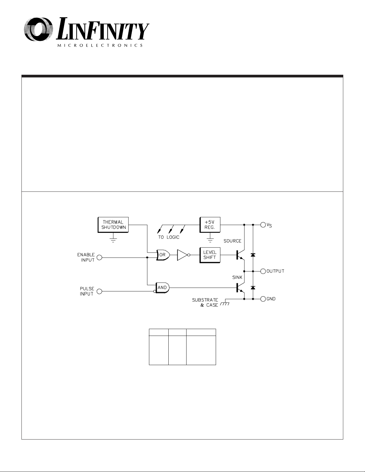
BLOCK DIAGRAM - SG1635/3635
FEATURES
••
• Source or sink 5A peak
••
••
• Half-bridge with internal diodes
••
••
• TTL input compatibility
••
••
• Either dual- or tri-state output
••
••
• Direct PWM motor drive from microprocessor
••
••
• Built-in thermal protection
••
••
• SG3635P replaces UDN2935Z
••
HIGH RELIABILITY FEATURES
- SG1635
♦♦
♦ Available to MIL-STD-883
♦♦
♦♦
♦ LMI level "S" processing available
♦♦
TRUTH TABLE
Enable Pulse Output
0 0 High
0 1 High
1 0 Low
1 1 Off - High Z
1 = Open or High
6/91 Rev 1.1 5/94 LINFINITY Microelectronics Inc.
Copyright 1994 11861 Western Avenue
1 (714) 898-8121
∞ ∞
∞ Garden Grove, CA 92841
∞ ∞
∞∞
∞ FAX: (714) 893-2570
∞∞

ABSOLUTE MAXIMUM RATINGS (Note 1)
Supply Voltage (VS)
SG1635/SG3635 ............................................................. 40V
Input Voltage
Enable and Pulse .............................................................. 7V
Source/Sink Output Current
Contiuous........................................................................... 3A
Peak................................................................................... 5A
Note 1. Values beyond which damage may occur.
THERMAL DATA
R Package:
Thermal ResistanceThermal Resistance-
P Package:
Junction to Case, θ
Junction to Ambient, θ
JC
................. 5.0°C/W
.............. 40°C/W
JA
Thermal Resistance-Junction to Case, θJT................ 4.0°C/W*
Thermal Resistance-Junction to Ambient, θJA............. 55°C/W
θθ
* =
θJT (Junction to Tab)
θθ
RECOMMENDED OPERATING CONDITIONS (Note 2)
Supply Voltage (VS)
SG1635/SG3635 .................................................... 8V to 35V
Note 2. Range over which the device is functional.
SG1635/SG3635
Operating Junction Temperature
Hermetic (R - Package)............................................... 150°C
Plastic (P - Package)................................................... 150°C
Storage Temperature Range ............................ -65°C to 150°C
Lead Temperature (Soldering, 10 Seconds) .................. 300°C
Note A. Junction Temperature Calculation: TJ = TA + (PD x θJA).
Note B. The above numbers for θ
thermal resistance of the package in a standard mounting configuration. The θ
guidelines for the thermal performance of the device/pcboard system. All of the above assume no ambient
airflow.
Source/Sink Output Current
Continuous......................................................................... 2A
Peak................................................................................... 3A
Operating Ambient Temperature Range
SG1635...........................................................-55°C to 125°C
SG3635................................................................ 0°C to 70°C
are maximums for the limiting
JC
numbers are meant to be
JA
ELECTRICAL CHARACTERISTICS
SG1635 and SG3635
(Unless otherwise specified, these specfiications apply over the operating ambient temperatures for SG1635 with -55°C ≤ TA ≤ 125°C, SG3635 with
0°C ≤ TA ≤ 70°C, and +VS = 24V. Low duty cycle pulse testing techniques are used which maintains junction and case temperatures equal to the ambient
temperature.)
Parameter Test Conditions
Static Characteristics
Logic 1 Input Voltage
Logic 0 Input Voltage
Input High Current
Input Low Current
Output Leakage
Source Saturation Voltage
Sink Saturation Voltage
Diode Forward Voltage
Supply Current
V
PULSE
V
PULSE
V
PULSE
V
V
V
PULSE
V
PULSE
I
DIODE
V
S
V
V
= V
= V
= V
= 24V
OUT
= 0V
OUT
= 2.0V, V
= 0.8V, V
= ±2A
= 35V
= 2.0V, V
PULSE
= 0.8V, V
PULSE
ENABLE
ENABLE
ENABLE
= 4.5V
= 0V
= 2.0V
ENABLE
ENABLE
ENABLE
ENABLE
= 0.8V, I
= 2.0V, I
= 0.8V
= 2.0V
OUT
OUT
= -2A
= 2A
SG1635/SG3635
Min. Typ. Max.
2.0 V
2.0
2.0
2.0
0.8
200
-3.2
500
40
3.0
3.0
3.0
25
70
Units
V
µA
mA
mA
mA
V
V
V
mA
mA
6/91 Rev 1.1 2/94 LINFINITY Microelectronics Inc.
Copyright 1994 11861 Western Avenue
2 (714) 898-8121
∞ ∞
∞ Garden Grove, CA 92841
∞ ∞
∞∞
∞ FAX: (714) 893-2570
∞∞
 Loading...