Microsemi Corporation SG1549Y, SG1549Y-883B, SG1549Y-DESC, SG2549M, SG2549Y Datasheet
...
4/90 Rev 1.1 2/94 LINFINITY Microelectronics Inc.
Copyright 1994 11861 Western Avenue
∞ ∞
∞ ∞
∞ Garden Grove, CA 92841
1 (714) 898-8121
∞∞
∞∞
∞ FAX: (714) 893-2570
SG1549/SG2549/SG3549
CURRENT SENSE LATCH
DESCRIPTION
This monolithic integrated circuit is an analog latch device with digital reset. It was
specifically designed to provide pulse-by-pulse current limiting for switch-mode power
supply systems, but many other application are also feasible. Its function is to provide
a latching switch action upon sensing an input threshold voltage, with reset accomplished by an external clock signal. This device can be interfaced directly with many
kinds of pulse width modulating control IC's, including the SG1524, SG1525A and
SG1527A.
The input threshold for the latch circuit is 100mV, which can be referenced either to
ground or to a wide-ranging positive voltage. There are high and low-going output
signals available, and both the supply voltage and clock signal can be taken directly
from an associated PWM control chip.
With delays in the range of 200 nanoseconds, this latch circuit is ideal for fast reaction
sensing to provide overall current limiting, short circuit protection, or transformer
saturation control.
FEATURES
••
••
• Current sensing with 100mV
threshold
••
••
• Common-mode input at ground or
to 40V
••
••
• Complementary outputs
••
••
• Automatic reset from PWM clock
••
••
• 180ns delay
••
••
• Interface direct to SG1524,
SG1525A, SG1527A
HIGH RELIABILITY FEATURES
- SG1549
♦♦
♦♦
♦ Available to MIL-STD-883
♦♦
♦♦
♦ LMI level "S" processing available
♦♦
♦♦
♦ Radiation data available
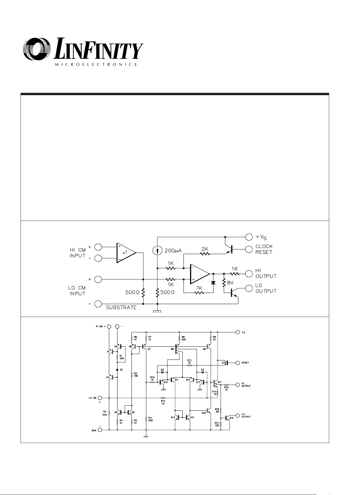
BLOCK DIAGRAM
SCHEMATIC

4/90 Rev 1.1 2/94 LINFINITY Microelectronics Inc.
Copyright 1994 11861 Western Avenue
∞ ∞
∞ ∞
∞ Garden Grove, CA 92841
2 (714) 898-8121
∞∞
∞∞
∞ FAX: (714) 893-2570
Operating Junction Temperature
Hermetic (Y Package) ..................................................
Plastic (N Package) ......................................................
Storage Temperature Range ............................
150°C
150°C
-65°C to 150°C
Input Supply Voltage, VS .....................................................
HI CM Input Voltage ............................................................
LO Output "off" Voltage .......................................................
LO Output "on" current .....................................................
25V
40V
40V
25mA
ABSOLUTE MAXIMUM RATINGS (Note 1)
SG1549/SG2549/SG3549
Note 1. Values beyond which damage may occur.
Y Package:
Thermal Resistance-
Junction to Case, θ
JC
.................. 50°C/W
Thermal Resistance-
Junction to Ambient, θ
JA
............ 130°C/W
M Package:
Thermal Resistance-
Junction to Case, θ
JC
.................. 60°C/W
Thermal Resistance-
Junction to Ambient, θ
JA
............. 95°C/W
THERMAL DATA
Note A. Junction Temperature Calculation: TJ = TA + (PD x θJA).
Note B. The above numbers for
θJC are maximums for the limiting
thermal resistance of the package in a standard mounting configuration. The θ
JA
numbers are meant to be
guidelines for the thermal performance of the device/pcboard system. All of the above assume no ambient
airflow.
Min. Trigger Voltage
Input Current
2.0202.5
40
2.0
20
V
µA
VCM = 2V, Pin 3 open, TA = 25°C
V
CM
= 40V, Pin 3 open, TA = 25°C
V
CM
= 2V, Pin 3 open
V
CM
= 40V, Pin 3 open
V
PIN 1
= V
PIN 2
= 40V
Threshold Voltage
Input Current
100
100
500
500
80
70
400
300
80
70
400
300
120
130
600
700
100
100
500
500
120
130
600
700
mV
mV
Ω
Ω
SG3549SG1549/2549
Test ConditionsParameter Units
V
PIN 8
= 5V
V
PIN 8
= 20V
Supply Current
Supply Section
2103
15
2
10
Note 3. Input threshold voltages and supply current are directly proportional to supply voltage, VS .
5.0V
2V to 40V
5V to 40V
0 to 10mA
0V to 0.8V
Reset HI Voltage ....................................................
Operating Ambient Temperature Range
SG1549Y .......................................................
SG2549Y or M .................................................
SG3549Y or M ....................................................
2.5V to 5.0V
-55°C to 125°C
-25°C to 85°C
0°C to 70°C
Note 2. Range over which the device is functional.
Input Supply Voltage, VS ....................................................
HI CM Input Voltage ..................................................
LO Output "off" Voltage .............................................
LO Output "on" Current .............................................
Reset LO Voltage .....................................................
RECOMMENDED OPERATING CONDITIONS (Note 2)
ELECTRICAL CHARACTERISTICS
(Unless otherwise specified, these specifications apply over the operating ambient temperatures for SG1549 with -55° C ≤ TA ≤ 125°C, SG2549 with
-25°C ≤ TA ≤ 85°C, SG3549 with 0°C ≤ TA ≤ 70°C, and VS = 5V. Low duty cycle pulse testing techniques are used which maintains junction and case
temperatures equal to the ambient temperature.)
Min. Typ. Max. Min. Typ. Max.
515mA
mA
LO CM Input Section (Note 3)
Pin 1 & 2 shorted, TA = 25°C
pin 1 & 2 shorted
V
PIN 3
= 50mV, TA = 25°C
V
PIN 3
= 50mV
Threshold Voltage
Input Impedance
HI CM Input Section
(Note 3)
100
100
100
100
200
120
120
130
130
300
80
80
70
70
120
120
130
130
300
mV
mV
mV
mV
µA
100
100
100
100
200
80
80
70
70
Clock Reset Section
V
PIN 7
= 4V
2.5
40
 Loading...