

120101
查询2N3418JAN供应商
TECHNICAL DATA
NPN MEDUIM POWER SILICON TRANSISTOR
Qualified per MIL-PRF-19500/393
Devices Qualified Level
2N3418
2N3814S
2N3419
2N3419S
2N3420
2N3420S
2N3421
2N3421S
MAXIMUM RATINGS
Collector-Emitter Voltage
Collector-Base Voltage
Emitter-Base Voltage
Collector Current
tP ≤ 1.0 ms, duty cycle ≤ 50%
Total Power Dissipation @ TA = +250C
@ TC = +1000C
Operating & Storage Temperature Range
1) Derate linearly 5.72 mW/0C for TA > 250C
2) Derate linearly 150 mW/0C for TC > 1000C
Ratings
(1)
(2)
ELECTRICAL CHARACTERISTICS
Characteristics Symbol Min. Max. Unit
OFF CHARACTERISTICS
Collector-Emitter Breakdown Current
IC = 50 mAdc, IB = 0 2N3418, S; 2N3420, S
2N3419, S; 2N3421, S
Collector-Emitter Cutoff Current
VBE = -0.5 Vdc, VCE = 80 Vdc 2N3418, S; 2N3420, S
VBE = -0.5 Vdc, VCE = 120 Vdc 2N3419, S; 2N3421, S
Collector-Emitter Cutoff Current
VCE = 45 Vdc, IB = 0 2N3418, S; 2N3420, S
VCE = 60 Vdc, IB = 0 2N3419, S; 2N3421, S
Emitter-Base Cutoff Current
VEB = 6.0 Vdc, IC = 0
VEB = 8.0 Vdc, IC = 0
Symbol
V
CEO
V
CBO
V
EBO
IC
PT
T
T
,
op
stg
2N3418, S
2N3420, S
60 80 Vdc
85 125 Vdc
2N3419, S
2N3421, S Unit
8.0 Vdc
3.0
5.0
1.0
15
-65 to +200
V
(BR)
I
I
I
CEX
CEO
EBO
CEO
Adc
W
W/0C
0
C
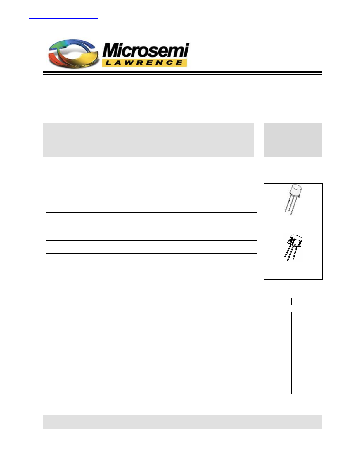
TO-39* (TO205-AD)
*See Appendix A for
Package Outline
60
80
JAN
JANTX
JANTXV
TO- 5*
2N3418, 2N3419,
2N3420, 2N3421
2N3418S, 2N3419S,
2N3420S, 2N3421S
Vdc
0.3
0.3
5.0
5.0
0.5
10
µAdc
µAdc
µAdc
6 Lake Street, Lawrence, MA 01841
1-800-446-1158 / (978) 794-1666 / Fax: (978) 689-0803
Page 1 of 2
120101
2N3418, S, 2N3419, S, 2N3420, S, 2N3421, S, JAN SERIES
ELECTRICAL CHARACTERISTICS
Characteristics Symbol Min. Max. Unit
ON CHARACTERISTICS
Forward-Current Transfer Ratio
I
= 100 mAdc, V
C
= 2.0 Vdc 2N3418, S; 2N3419, S
CE
2N3420, S; 2N3421, S
I
= 1.0 Adc, V
C
= 2.0 Vdc 2N3418, S; 2N3419, S
CE
2N3420, S; 2N3421, S
I
= 2.0 Adc, V
C
= 2.0 Vdc 2N3418, S; 2N3419, S
CE
2N3420, S; 2N3421, S
IC = 5.0 Adc, VCE = 5.0 Vdc 2N3418, S; 2N3419, S
2N3420, S; 2N3421, S
Base-Emitter Saturation Voltage
IC = 1.0 Adc, IB = 0.1 Adc
IC = 2.0 Adc, IB = 0.2 Adc
Collector-Emitter Saturation Voltage
IC = 1.0 Adc, IB = 0.1 Adc
IC = 2.0 Adc, IB = 0.2 Adc
DYNAMIC CHARACTERISTICS
Magnitude of Common Emitter Small-Signal Short Circuit
Forward Current Transfer Ratio
I
= 0.1 Adc, V
C
= 10 Vdc, f = 20 MHz
CE
Output Capacitance
VCB = 10 Vdc, IE = 0, 100 kHz ≤ f ≤ 1.0 MHz
SWITCHING CHARACTERISTICS
Delay Time
Rise Time
Storage Time
Fall Time
SAFE OPERATING AREA
DC Tests
TC = 1000C, 1 Cycle, t = 1.0 s
Test 1
VCE = 5.0 Vdc, IC = 3.0 Adc
Test 2
VCE = 37 Vdc, IC = 0.4 Adc
TEST 3
VCE = 60 Vdc, IC = 0.185 Adc 2N3418, S; 2N3420, S
VCE = 80 Vdc, IC = 0.12 Adc 2N3419, S; 2N3421, S
V
= -3.7 Vdc
BE(off)
IC = 1.0 Adc, I
V
= -3.7 Vdc
BE(off)
IC = 1.0 Adc, I
= 100 mAdc
B1
= -100 mAdc
B2
Clamped Switching
T
= 250C, I
A
= 0.5 Adc, IC = 3.0 Adc
B
hFE
V
BE(sat)
V
CE(sat)
hfe
C
obo
t
d
t
r
t
s
tf
20
40
20
40
60
120
15
30
10
15
0.6
0.7
1.2
1.4
0.25
Vdc
Vdc
0.5
1.3
0.08
0.22
1.10
0.20
8.0
150
pF
µs
µs
µs
µs
6 Lake Street, Lawrence, MA 01841
1-800-446-1158 / (978) 794-1666 / Fax: (978) 689-0803
Page 2 of 2
 Loading...