

Microchip Technology Inc PIC16C923T-04-PT, PIC16C923T-04I-CL, PIC16C923T-04I-L, PIC16C923T-04I-PT, PIC16C923T-04I-SP Datasheet
...
PIC16C9XX
8-Bit CMOS Microcontroller with LCD Driver
Devices included in this data sheet:
• PIC16C923
• PIC16C924
Microcontroller Core Features:
• High performance RISC CPU
• Only 35 single word instructions to learn
• 4K x 14 on-chip EPROM program memory
• 176 x 8 general purpose registers (SRAM)
• All single cycle instructions (500 ns) except for
program branches which are two-cycle
• Operating speed: DC - 8 MHz clock input
DC - 500 ns instruction cycle
• Interrupt capability
• Eight level deep hardware stack
• Direct, indirect and relative addressing modes
Peripheral Features:
• 25 I/O pins with individual direction control
• 25-27 input only pins
• Timer0: 8-bit timer/counter with 8-bit prescaler
• Timer1: 16-bit timer/counter, can be incremented
during sleep via external crystal/clock
• Timer2: 8-bit timer/counter with 8-bit period register, prescaler and postscaler
• One pin that can be configured a capture input,
PWM output, or compare output
- Capture is 16-bit, max. resolution 31.25 ns
- Compare is 16-bit, max. resolution 500 ns
- PWM max resolution is 10-bits.
Maximum PWM frequency @ 8-bit resolution
= 32 kHz, @ 10-bit resolution = 8 kHz
• Programmable LCD timing module
- Multiple LCD timing sources available
- Can drive LCD panel while in Sleep mode
- Static, 1/2, 1/3, 1/4 multiplex
- Static drive and 1/3 bias capability
- 16 bytes of dedicated LCD RAM
- Up to 32 segments, up to 4 commons
Common Segment Pixels
13232
23162
33090
4 29 116
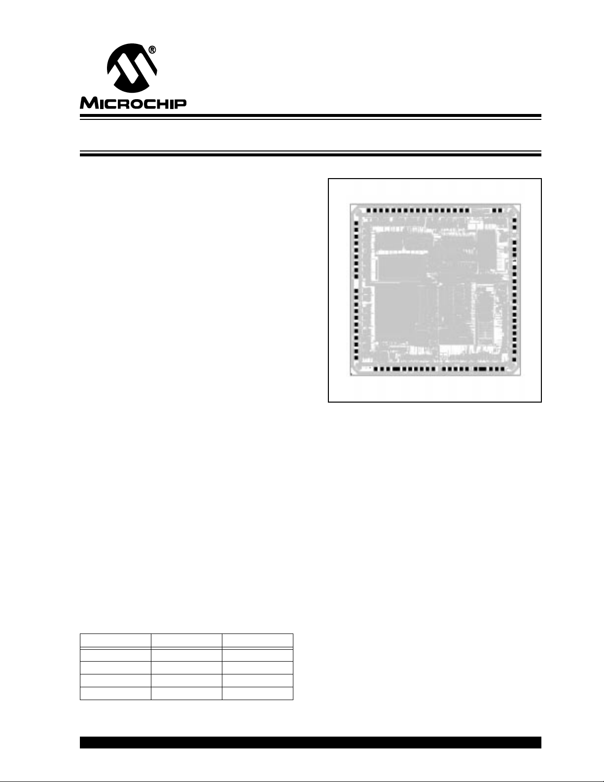
Available in Die Form
• Synchronous Serial Port (SSP) with SPI
2
and I
• 8-bit multi-channel Analog to Digital converter
(PIC16C924 only)
C
Special Microcontroller Features:
• Power-on Reset (POR)
• Power-up Timer (PWRT) and Oscillator Start-up
Timer (OST)
• Watchdog Timer (WDT) with its own on-chip RC
oscillator for reliable operation
• Programmable code-protection
• Power saving SLEEP mode
• Selectable oscillator options
• In-Circuit Serial Programming™ (via two pins)
CMOS Tec hnology
• Low-power, high-speed CMOS EPROM
technology
• Fully static design
• Wide operating voltage range: 2.5V to 6.0V
• Commercial and Industrial temperature ranges
• Low-power consumption:
- < 2 mA @ 5.5V, 4 MHz
- 22.5 µ A typical @ 4V, 32 kHz
- < 1 µ A typical standby current @ 3.0V
ICSP is a trademark of Microchip Technology Inc. I
1997 Microchip Technology Inc. DS30444E - page 1
2
C is a trademark of Philips Corporation. SPI is a trademark of Motorola Corporation.
PIC16C9XX
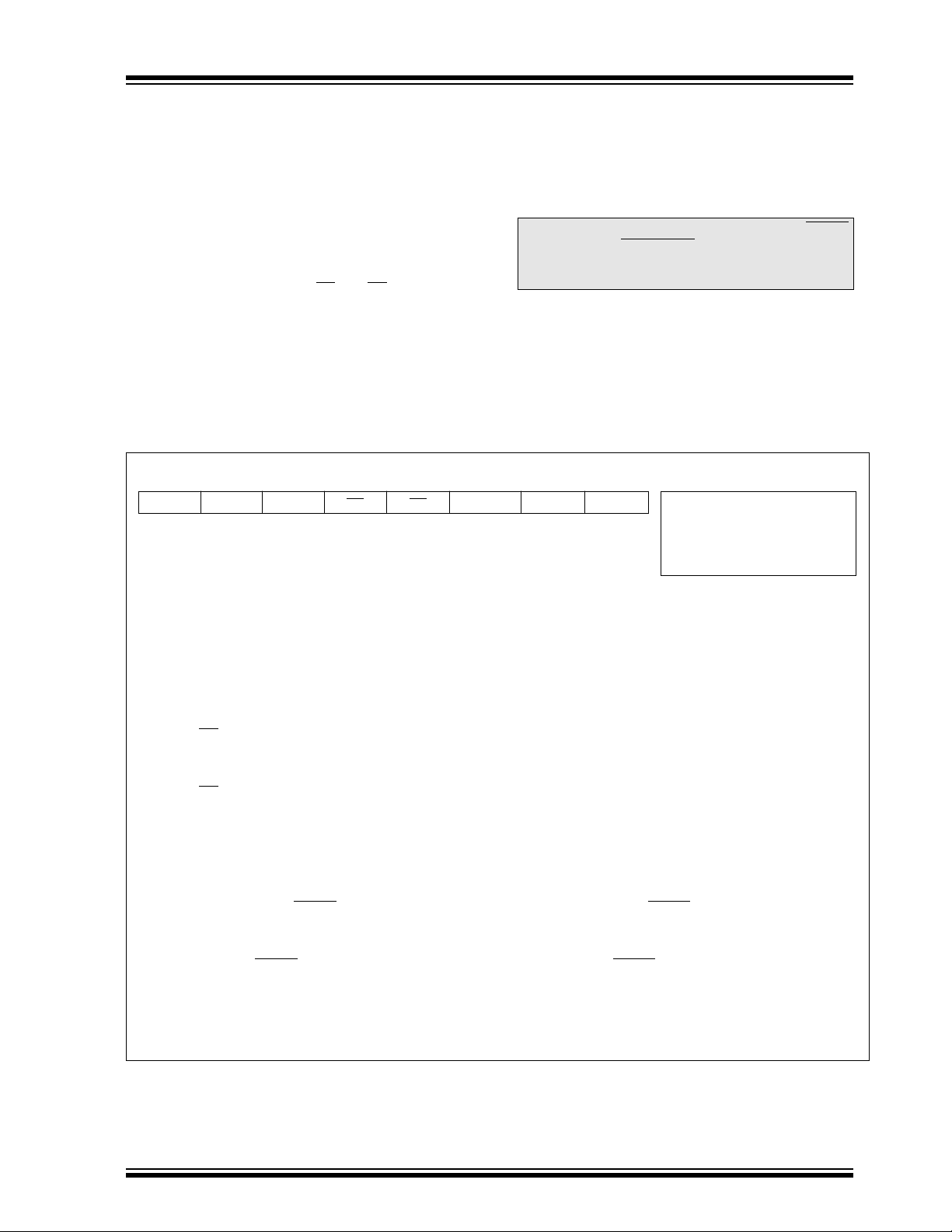
Pin Diagrams
Shrink PDIP (750 mil)
MCLR/VPP
RB3
RB2
RA0
RA1
V
RA2
RA3
RA4/T0CKI
RA5/SS
RB1
RB0/INT
RC3/SCK/SCL
RC4/SDI/SDA
RC5/SDO
V
LCD2
V
LCD3
V
VSS
OSC1/CLKIN
OSC2/CLKOUT
RC0/T1OSO/T1CKI
RC1/T1OSI
RC2/CCP1
VLCD1
VLCDADJ
RD0/SEG00
RD1/SEG01
RD2/SEG02
RD3/SEG03
SS
C1
C2
DD
1
2
3
4
5
6
7
8
9
10
11
12
13
14
15
16
17
18
19
20
21
22
23
24
25
26
27
28
29
30
31
32
64
63
62
61
60
59
58
57
56
55
54
PIC16C923
53
52
51
50
49
48
47
46
45
44
43
42
41
40
39
38
37
36
35
34
33
RC0/T1OSO/T1CKI
RB4
RB5
RB7
RB6
DD
V
COM0
RD7/SEG31/COM1
RD6/SEG30/COM2
RD5/SEG29/COM3
RG6/SEG26
RG5/SEG25
RG4/SEG24
RG3/SEG23
RG2/SEG22
RG1/SEG21
RG0/SEG20
RF7/SEG19
RF6/SEG18
RF5/SEG17
RF4/SEG16
RF3/SEG15
RF2/SEG14
RF1/SEG13
RF0/SEG12
RE6/SEG11
RE5/SEG10
RE4/SEG09
RE3/SEG08
RE2/SEG07
RE1/SEG06
RE0/SEG05
RD4/SEG04
RA4/T0CKI
RC3/SCK/SCL
RC4/SDI/SDA
RC5/SDO
OSC1/CLKIN
OSC2/CLKOUT
RC0/T1OSO/T1CKI
PLCC
RA4/T0CKI
RA5/SS
RB0/INT
RC3/SCK/SCL
RC4/SDI/SDA
RC5/SDO
V
LCD2
V
LCD3
OSC1/CLKIN
OSC2/CLKOUT
RA5/SS
RB1
RB0/INT
C1
C2
V
LCD2
V
LCD3
VDD
VSS
RB1
V
VDD
VSS
/VPP
RA3
RA2
VSSRA1
RA0
RB2
RB3
MCLR
N/C
RB4
RB5
RB7
RB6
VDDCOM0
RD7/SEG31/COM1
RD6/SEG30/COM2
987654321
10
11
12
13
14
15
C1
C2
DD
16
17
PIC16C923
18
19
20
21
22
23
24
25
26
2728293031323334353637383940414243
LCD1
V
VLCDADJ
RC2/CCP1
RC1/T1OSI
RA3
RA2
VSSRA1
RA0
RB2
646362616059585756555453525150
1
2
3
4
5
6
7
8
PIC16C923
9
10
11
12
13
14
15
16
171819202122232425262728293031
RD0/SEG00
RD1/SEG01
RD2/SEG02
RD3/SEG03
MCLR/VPP
RB4
RB3
68676665646362
RE7/SEG27
RE0/SEG05
RE1/SEG06
RE2/SEG07
RD4/SEG04
VDDCOM0
RB5
RB7
RB6
61
60
59
58
57
56
55
54
53
52
51
50
49
48
47
46
45
44
RE3/SEG08
RE4/SEG09
RE6/SEG11
RE5/SEG10
RD7/SEG31/COM1
TQFP
RD6/SEG30/COM2
49
48
47
46
45
44
43
42
41
40
39
38
37
36
35
34
33
32
RD5/SEG29/COM3
RG6/SEG26
RG5/SEG25
RG4/SEG24
RG3/SEG23
RG2/SEG22
RG1/SEG21
RG0/SEG20
RG7/SEG28
RF7/SEG19
RF6/SEG18
RF5/SEG17
RF4/SEG16
RF3/SEG15
RF2/SEG14
RF1/SEG13
RF0/SEG12
RD5/SEG29/COM3
RG6/SEG26
RG5/SEG25
RG4/SEG24
RG3/SEG23
RG2/SEG22
RG1/SEG21
RG0/SEG20
RF7/SEG19
RF6/SEG18
RF5/SEG17
RF4/SEG16
RF3/SEG15
RF2/SEG14
RF1/SEG13
RF0/SEG12
LEGEND:
Input Pin
Output Pin
Input/Output Pin
Digital Input/LCD Output Pin
LCD Output Pin
DS30444E - page 2
LCD1
V
RC2/CCP1
RC1/T1OSI
VLCDADJ
RD0/SEG00
RD1/SEG01
RE0/SEG05
RD2/SEG02
RD3/SEG03
RD4/SEG04
RE1/SEG06
RE2/SEG07
RE3/SEG08
RE4/SEG09
RE6/SEG11
RE5/SEG10
1997 Microchip Technology Inc.
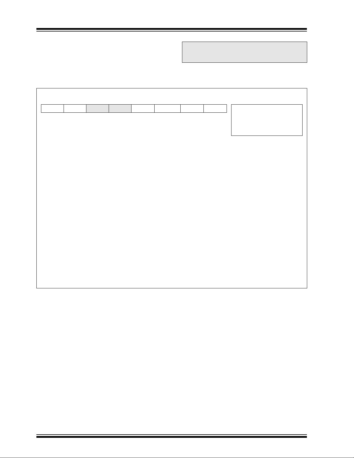
Pin Diagrams (Cont.’d)
PIC16C9XX
Shrink PDIP (750 mil)
MCLR/VPP
RB3
RB2
RA0/AN0
RA1/AN1
VSS
RA2/AN2
RA3/AN3/V
REF
RA4/T0CKI
RA5/AN4/SS
RB1
RB0/INT
RC3/SCK/SCL
RC4/SDI/SDA
RC5/SDO
V
LCD2
V
LCD3
V
VSS
OSC1/CLKIN
OSC2/CLKOUT
RC0/T1OSO/T1CKI
RC1/T1OSI
RC2/CCP1
LCD1
V
VLCDADJ
RD0/SEG00
RD1/SEG01
RD2/SEG02
RD3/SEG03
C1
C2
DD
1
2
3
4
5
6
7
8
9
10
11
12
13
14
15
16
17
18
19
20
21
22
23
24
25
26
27
28
29
30
31
32
64
63
62
61
60
59
58
57
56
55
54
PIC16C924
53
52
51
50
49
48
47
46
45
44
43
42
41
40
39
38
37
36
35
34
33
RC0/T1OSO/T1CKI
RB4
RB5
RB7
RB6
V
DD
COM0
RD7/SEG31/COM1
RD6/SEG30/COM2
RD5/SEG29/COM3
RG6/SEG26
RG5/SEG25
RG4/SEG24
RG3/SEG23
RG2/SEG22
RG1/SEG21
RG0/SEG20
RF7/SEG19
RF6/SEG18
RF5/SEG17
RF4/SEG16
RF3/SEG15
RF2/SEG14
RF1/SEG13
RF0/SEG12
RE6/SEG11
RE5/SEG10
RE4/SEG09
RE3/SEG08
RE2/SEG07
RE1/SEG06
RE0/SEG05
RD4/SEG04
RA4/T0CKI
RA5/AN4/SS
RC3/SCK/SCL
RC4/SDI/SDA
RC5/SDO
OSC1/CLKIN
OSC2/CLKOUT
RC0/T1OSO/T1CKI
PLCC
RA4/T0CKI
RA5/AN4/SS
RB0/INT
RC3/SCK/SCL
RC4/SDI/SDA
RC5/SDO
V
V
A
OSC1/CLKIN
OSC2/CLKOUT
TQFP
RB1
RB0/INT
C1
C2
V
LCD2
V
LCD3
VDD
VSS
RB1
LCD2
LCD3
VDD
VDD
VSS
/VPP
RA3/AN3/VREF
RA2/AN2
VSSRA1/AN1
RA0/AN0
RB2
RB3
MCLR
N/C
RB4
RB5
RB7
RB6
VDDCOM0
RD7/SEG31/COM1
RD6/SEG30/COM2
987654321
10
11
12
13
14
15
C1
C2
16
17
PIC16C924
18
19
20
21
22
23
24
25
26
2728293031323334353637383940414243
LCD1
V
VLCDADJ
RC2/CCP1
RC1/T1OSI
RA3/AN3/VREF
RA2/AN2
VSSRA1/AN1
RA0/AN0
RB2
646362616059585756555453525150
1
2
3
4
5
6
7
8
PIC16C924
9
10
11
12
13
14
15
16
171819202122232425262728293031
RD0/SEG00
RD1/SEG01
RD2/SEG02
RD3/SEG03
MCLR/VPP
RB4
RB3
68676665646362
RE7/SEG27
RE0/SEG05
RE1/SEG06
RE2/SEG07
RD4/SEG04
VDDCOM0
RB5
RB7
RB6
61
60
59
58
57
56
55
54
53
52
51
50
49
48
47
46
45
44
RE3/SEG08
RE4/SEG09
RE6/SEG11
RE5/SEG10
RD7/SEG31/COM1
RD6/SEG30/COM2
49
48
47
46
45
44
43
42
41
40
39
38
37
36
35
34
33
32
RD5/SEG29/COM3
RG6/SEG26
RG5/SEG25
RG4/SEG24
RG3/SEG23
RG2/SEG22
RG1/SEG21
RG0/SEG20
RG7/SEG28
RF7/SEG19
RF6/SEG18
RF5/SEG17
RF4/SEG16
RF3/SEG15
RF2/SEG14
RF1/SEG13
RF0/SEG12
RD5/SEG29/COM3
RG6/SEG26
RG5/SEG25
RG4/SEG24
RG3/SEG23
RG2/SEG22
RG1/SEG21
RG0/SEG20
RF7/SEG19
RF6/SEG18
RF5/SEG17
RF4/SEG16
RF3/SEG15
RF2/SEG14
RF1/SEG13
RF0/SEG12
LCD1
LEGEND:
Input Pin
Output Pin
Input/Output Pin
V
RC2/CCP1
RC1/T1OSI
VLCDADJ
RD0/SEG00
RD1/SEG01
RE0/SEG05
RD2/SEG02
RD3/SEG03
RD4/SEG04
RE1/SEG06
RE2/SEG07
RE3/SEG08
RE4/SEG09
RE6/SEG11
RE5/SEG10
Digital Input/LCD Output Pin
LCD Output Pin
1997 Microchip Technology Inc. DS30444E - page 3

PIC16C9XX
Table of Contents
1.0 General Description..................................................................................................................................................................... 5
2.0 PIC16C9XX Device Varieties...................................................................................................................................................... 7
3.0 Architectural Overview ................................................................................................................................................................ 9
4.0 Memory Organization................................................................................................................................................................ 17
5.0 Ports.......................................................................................................................................................................................... 31
6.0 Overview of Timer Modules....................................................................................................................................................... 43
7.0 Timer0 Module .......................................................................................................................................................................... 45
8.0 Timer1 Module .......................................................................................................................................................................... 51
9.0 Timer2 Module .......................................................................................................................................................................... 55
10.0 Capture/Compare/PWM (CCP) Module .................................................................................................................................... 57
11.0 Synchronous Serial Port (SSP) Module .................................................................................................................................... 63
12.0 Analog-to-Digital Converter (A/D) Module.................................................................................................................................79
13.0 LCD Module .............................................................................................................................................................................. 89
14.0 Special Features of the CPU...................................................................................................................................................103
15.0 Instruction Set Summary......................................................................................................................................................... 119
16.0 Development Support.............................................................................................................................................................. 137
17.0 Electrical Characteristics......................................................................................................................................................... 141
18.0 DC and AC Characteristics Graphs and Tables......................................................................................................................161
19.0 Packaging Information............................................................................................................................................................. 171
Appendix A: ................................................................................................................................................................................... 175
Appendix B: Compatibility ............................................................................................................................................................. 175
Appendix C: What’s New................................................................................................................................................................ 176
Appendix D: What’s Changed........................................................................................................................................................ 176
Index .................................................................................................................................................................................................. 177
List of Equations And Examples ........................................................................................................................................................ 181
List of Figures..................................................................................................................................................................................... 181
List of Tables...................................................................................................................................................................................... 182
Reader Response.............................................................................................................................................................................. 186
PIC16C9XX Product Identification System........................................................................................................................................ 187
To Our Valued Customers
We constantly strive to improve the quality of all our products and documentation. We have spent an exceptional
amount of time to ensure that these documents are correct. However, we realize that we may have missed a few
things. If you find any information that is missing or appears in error, please use the reader response form in the
back of this data sheet to inform us. We appreciate your assistance in making this a better document.
DS30444E - page 4
1997 Microchip Technology Inc.

PIC16C9XX
1.0 GENERAL DESCRIPTION
The PIC16C9XX is a family of
mance, CMOS, fully-static, 8-bit microcontrollers with
an integrated LCD Driver module, in the PIC16CXXX
mid-range family.
All PICmicro™ microcontrollers employ an advanced
RISC architecture. The PIC16CXXX microcontroller
family has enhanced core features, eight-level deep
stack, and multiple internal and external interrupt
sources. The separate instruction and data buses of the
Harvard architecture allow a 14-bit wide instruction
word with the separate 8-bit wide data. The two stage
instruction pipeline allows all instructions to execute in
a single cycle, except for program branches (which
require two cycles). A total of 35 instructions (reduced
instruction set) are available. Additionally, a large register set gives some of the architectural innov ations used
to achieve a very high performance.
PIC16CXXX microcontrollers typically achieve a 2:1
code compression and a 4:1 speed improvement over
other 8-bit microcontrollers in their class.
The PIC16C923 devices have 176 bytes of RAM and
25 I/O pins. In addition several peripheral features are
available including: three timer/counters, one Capture/Compare/PWM module, one serial port and one
LCD module. The Synchronous Serial P ort can be configured as either a 3-wire Serial Peripheral Interface
(SPI) or the two-wire Inter-Integrated Circuit (I
The LCD module features programmable multiplex
mode (static, 1/2, 1/3 and 1/4) and drive bias (static and
1/3). It is capable of driving up to 32 segments and up
to 4 commons. It can also drive the LCD panel while in
SLEEP mode.
The PIC16C924 devices have 176 bytes of RAM and
25 I/O pins. In addition several peripheral features are
available including: three timer/counters, one Capture/Compare/PWM module, one serial port and one
LCD module. The Synchronous Serial P ort can be configured as either a 3-wire Serial Peripheral Interface
(SPI) or the two-wire Inter-Integrated Circuit (I
The LCD module features programmable multiplex
mode (static, 1/2, 1/3 and 1/4) and drive bias (static and
1/3). It is capable of driving up to 32 segments and up
to 4 commons. It can also drive the LCD panel while in
SLEEP mode. The PIC16C924 also has an 5-channel
high-speed 8-bit A/D. The 8-bit resolution is ideally
suited for applications requiring low-cost analog interface, e.g. thermostat control, pressure sensing, and
meters.
The PIC16C9XX family has special features to reduce
external components, thus reducing cost, enhancing
system reliability and reducing power consumption.
There are four oscillator options, of which the single pin
RC oscillator provides a low-cost solution, the LP oscillator minimizes power consumption, XT is a standard
crystal, and the HS is for High Speed crystals. The
SLEEP (power-down) feature provides a power saving
low-cost, high-perfor-
2
C) bus.
2
C) bus.
mode. The user can wake up the chip from SLEEP
through several external and internal interrupts and
reset(s).
A highly reliable Watchdog Timer with its own on-chip
RC oscillator provides recovery in the event of a software lock-up.
A UV erasable CERQUAD (compatible with PLCC)
packaged version is ideal for code development while
the cost-effective One-Time-Programmable (OTP) version is suitable for production in any volume.
The PIC16C9XX family fits perfectly in applications
ranging from handheld meters, thermostats, to home
security products. The EPROM technology makes customization of application programs (LCD panels, calibration constants, sensor interfaces, etc.) extremely
fast and conv enient. The small f ootprint packages make
this microcontroller series perfect for all applications
with space limitations. Low cost, low pow er, high perf ormance, ease of use and I/O flexibility make the
PIC16C9XX very versatile even in areas where no
microcontroller use has been considered before (e.g.
timer functions, capture and compare, PWM functions
and coprocessor applications).
1.1 F
Users familiar with the PIC16C5X microcontroller family
will realize that this is an enhanced version of the
PIC16C5X architecture. Please refer to Appendix A for
a detailed list of enhancements. Code written for the
PIC16C5X can be easily ported to the PIC16CXXX
family of devices (Appendix B).
1.2 De
PIC16C9XX devices are supported by the complete
line of Microchip Development tools.
Please refer to Section 16.0 for more details about
Microchip’s development tools.
amily and Upward Compatibility
velopment Support
1997 Microchip Technology Inc. DS30444E- page 5
PIC16C9XX
TABLE 1-1: PIC16C9XX FAMILY OF DEVICES
PIC16C923
Clock
Memory
Peripherals
Features
All PICmicro Family devices ha v e Power-on Reset, selectable Watchdog Timer, selectable code protect and high I/O current capability . All PIC16C9XX Family devices use serial programming with clock pin RB6 and data pin RB7.
Maximum Frequency of Operation (MHz) 8 8
EPROM Program Memory 4K 4K
Data Memory (bytes) 176 176
Timer Module(s) TMR0,
TMR1,
TMR2
Capture/Compare/PWM Module(s) 1 1
Serial Port(s)
2
(SPI/I
C, USART)
Parallel Slave Port — —
A/D Converter (8-bit) Channels — 5
LCD Module 4 Com,
Interrupt Sources 8 9
I/O Pins 25 25
Input Pins 27 27
Voltage Range (Volts) 2.5-6.0 2.5-6.0
In-Circuit Serial Programming Yes Yes
Brown-out Reset — —
Packages 64-pin SDIP,
2
SPI/I
C SPI/I
32 Seg
TQFP;
68-pin PLCC,
Die
PIC16C924
TMR0,
TMR1,
TMR2
2
C
4 Com,
32 Seg
64-pin SDIP,
TQFP;
68-pin PLCC,
Die
DS30444E - page 6
1997 Microchip Technology Inc.

PIC16C9XX
2.0 PIC16C9XX DEVICE VARIETIES
A variety of frequency ranges and packaging options
are available . Depending on application and production
requirements, the proper device option can be selected
using the information in the PIC16C9XX Product Identification System section at the end of this data sheet.
When placing orders, please use that page of the data
sheet to specify the correct part number.
For the PIC16C9XX family, there are two device “types”
as indicated in the device number:
1. C , as in PIC16 C 924. These devices have
EPROM type memory and operate over the
standard voltage range.
2. LC , as in PIC16 LC 924. These devices have
EPROM type memory and operate over an
extended voltage range.
2.1 UV Erasab
The UV erasable version, offered in CERQUAD package, is optimal for prototype dev elopment and pilot programs.
The UV erasable version can be erased and reprogrammed to any of the configuration modes.
Microchip's PICSTART
grammers both support the PIC16C9XX. Third party
programmers also are available; refer to the
Third Party Guide
le Devices
Plus and PRO MATE
for a list of sources.
II pro-
Microchip
2.3 Quic
k-Turnaround-Production (QTP)
Devices
Microchip offers a QTP Programming Service for factory production orders. This service is made available
for users who choose not to program a medium to high
quantity of units and whose code patterns have stabilized. The devices are identical to the OTP devices but
with all EPROM locations and configuration options
already programmed by the factory. Certain code and
prototype verification procedures apply before production shipments are available. Please contact your local
Microchip Technology sales office for more details.
2.4 Serializ
Production (SQTP
Microchip offers a unique programming service where
a few user-defined locations in each device are programmed with different serial numbers. The serial numbers may be random, pseudo-random or sequential.
Serial programming allows each device to have a
unique number which can serve as an entry-code,
password or ID number.
ed Quick-Turnaround
SM
) De
vices
2.2 One-Time-Pr
ogrammable (OTP)
Devices
The availability of OTP devices is especially useful for
customers who need the flexibility for frequent code
updates and small volume applications.
The OTP devices , packaged in plastic packages, permit
the user to program them once. In addition to the program memory, the configuration bits must also be programmed.
1997 Microchip Technology Inc. DS30444E - page 7

PIC16C9XX
NOTES:
DS30444E - page 8
1997 Microchip Technology Inc.

PIC16C9XX
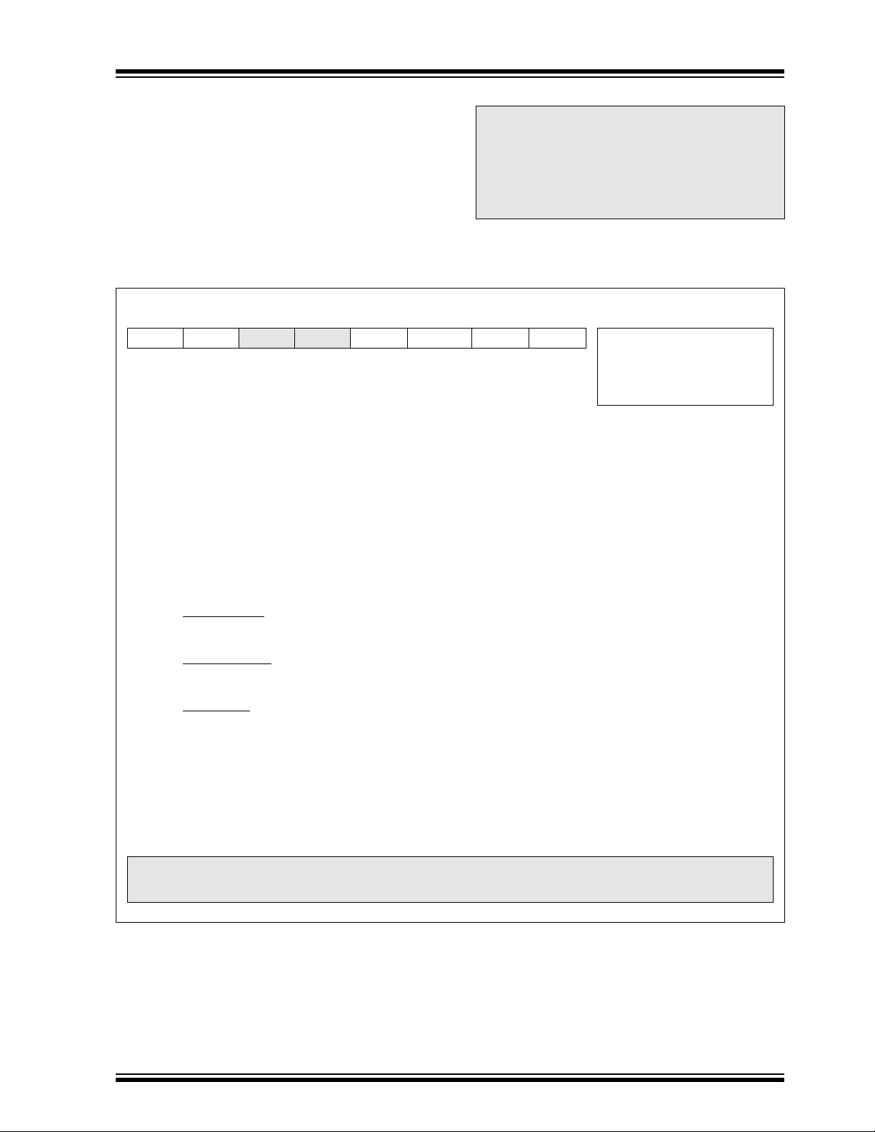
3.0 ARCHITECTURAL OVERVIEW
The high performance of the PIC16CXXX family can be
attributed to a number of architectural features commonly found in RISC microprocessors. To begin with,
the PIC16CXXX uses a Harvard architecture, in which,
program and data are accessed from separate memories using separate buses. This improves bandwidth
over traditional von Neumann architecture where program and data are fetched from the same memory
using the same bus. Separating program and data
buses further allows instructions to be sized differently
than the 8-bit wide data word. Instruction opcodes are
14-bits wide making it possible to have all single word
instructions. A 14-bit wide progr am memory access bus
fetches a 14-bit instruction in a single cycle. A
two-stage pipeline overlaps fetch and execution of
instructions (Example 3-1). Consequently, all instructions execute in a single cycle (500 ns @ 8 MHz) e xcept
for program branches.
The PIC16C923 and PIC16C924 both address 4K x 14
of program memory and 176 x 8 of data memory.
The PIC16CXXX can directly or indirectly address its
register files or data memory. All special function registers, including the program counter, are mapped in the
data memory. The PIC16CXXX has an orthogonal
(symmetrical) instruction set that makes it possible to
carry out any operation on any register using any
addressing mode. This symmetrical nature and lack of
‘special optimal situations’ make programming with the
PIC16CXXX simple yet efficient, thus significantly
reducing the learning curve.
PIC16CXXX devices contain an 8-bit ALU and working
register. The ALU is a general purpose ar ithmetic unit.
It performs arithmetic and Boolean functions between
the data in the working register and any register file.
The ALU is 8-bits wide and capable of addition, subtraction, shift and logical operations. Unless otherwise
mentioned, arithmetic operations are two's complement in nature. In two-operand instructions, typically
one operand is the working register (W register). The
other operand is a file register or an immediate constant. In single operand instructions, the operand is
either the W register or a file register.
The W register is an 8-bit working register used f or ALU
operations. It is not an addressable register.
Depending on the instruction executed, the ALU may
affect the values of the Carry (C), Digit Carry (DC), and
Zero (Z) bits in the STATUS register. The C and DC bits
operate as a borro
respectively, in subtraction. See the SUBLW and SUBWF
instructions for examples.
w bit and a digit borrow out bit,
1997 Microchip Technology Inc. DS30444E - page 9

PIC16C9XX
FIGURE 3-1: PIC16C923 BLOCK DIAGRAM
Program
Bus
OSC1/CLKIN
OSC2/CLKOUT
EPROM
Program
Memory
4K x 14
14
Instruction reg
Instruction
Decode &
Control
Timing
Generation
13
Program Counter
8 Level Stack
Direct Addr
8
Power-up
Oscillator
Start-up Timer
Power-on
Watchdog
MCLR
(13-bit)
Timer
Reset
Timer
VDD, VSS
RAM Addr
7
8
Data Bus
RAM
File
Registers
176 x 8
Addr MUX
FSR reg
STATUS reg
3
ALU
W reg
9
MUX
Indirect
8
8
Addr
PORTA
PORTB
PORTC
PORTD
PORTE
RA0
RA1
RA2
RA3
RA4/T0CKI
RA5/SS
RB0/INT
RB1-RB7
RC0/T1OSO/T1CKI
RC1/T1OSI
RC2/CCP1
RC3/SCK/SCL
RC4/SDI/SDA
RC5/SDO
RD0-RD4/SEGnn
RD5-RD7/SEGnn/COMn
Timer0
Synchronous
Serial Port
Timer1, Timer2,
CCP1
LCD
PORTF
PORTG
RE0-RE7/SEGnn
RF0-RF7/SEGnn
RG0-RG7/SEGnn
COM0
VLCD1
VLCD2
LCD3
V
C1
C2
VLCDADJ
DS30444E - page 10
1997 Microchip Technology Inc.
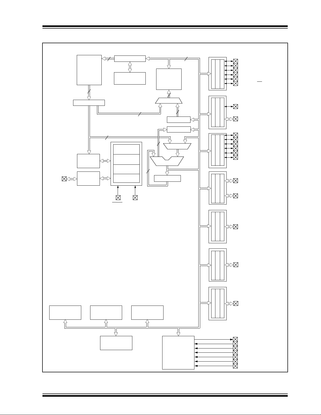
FIGURE 3-2: PIC16C924 BLOCK DIAGRAM
PIC16C9XX
Program
Bus
OSC1/CLKIN
OSC2/CLKOUT
EPROM
Program
Memory
4K x 14
14
Instruction reg
Instruction
Decode &
Control
Timing
Generation
13
Program Counter
8 Level Stack
Direct Addr
8
Power-up
Oscillator
Start-up Timer
Power-on
Watchdog
MCLR
(13-bit)
Timer
Reset
Timer
VDD, VSS
RAM Addr
7
8
Data Bus
RAM
File
Registers
176 x 8
Addr MUX
FSR reg
STATUS reg
3
ALU
W reg
9
MUX
Indirect
8
8
Addr
PORTA
PORTB
PORTC
PORTD
PORTE
RA0/AN0
RA1/AN1
RA2/AN2
RA3/AN3/VREF
RA4/T0CKI
RA5/AN4/SS
RB0/INT
RB1-RB7
RC0/T1OSO/T1CKI
RC1/T1OSI
RC2/CCP1
RC3/SCK/SCL
RC4/SDI/SDA
RC5/SDO
RD0-RD4/SEGnn
RD5-RD7/SEGnn/COMn
Timer0
A/D
Synchronous
Serial Port
Timer1, Timer2,
CCP1
LCD
PORTF
PORTG
RE0-RE7/SEGnn
RF0-RF7/SEGnn
RG0-RG7/SEGnn
COM0
VLCD1
VLCD2
LCD3
V
C1
C2
VLCDADJ
1997 Microchip Technology Inc. DS30444E - page 11

PIC16C9XX
TABLE 3-1: PIC16C9XX PINOUT DESCRIPTION
DIP
Pin Name
OSC1/CLKIN 22 24 14 I ST/CMOS Oscillator crystal input or external clock source input. This
OSC2/CLKOUT 23 25 15 O — Oscillator crystal output. Connects to crystal or resonator
MCLR/VPP 1 2 57 I/P ST Master clear (reset) input or programming voltage input.
RA0/AN0 4 5 60 I/O TTL RA0 can also be Analog input0.
RA1/AN1 5 6 61 I/O TTL RA1 can also be Analog input1.
RA2/AN2 7 8 63 I/O TTL RA2 can also be Analog input2.
RA3/AN3/VREF 8 9 64 I/O TTL RA3 can also be Analog input3 or A/D Voltage Refer-
RA4/T0CKI 9 10 1 I/O ST RA4 can also be the clock input to the Timer0
RA5/AN4/SS 10 11 2 I/O TTL RA5 can be the slave select for the synchronous serial
RB0/INT 12 13 4 I/O TTL/ST RB0 can also be the external interrupt pin. This buffer
RB1 11 12 3 I/O TTL
RB2 3 4 59 I/O TTL
RB3 2 3 58 I/O TTL
RB4 64 68 56 I/O TTL Interrupt on change pin.
RB5 63 67 55 I/O TTL Interrupt on change pin.
RB6 61 65 53 I/O TTL/ST Interrupt on change pin. Serial programming clock.
RB7 62 66 54 I/O TTL/ST Interrupt on change pin. Serial programming data.
RC0/T1OSO/T1CKI 24 26 16 I/O ST RC0 can also be the Timer1 oscillator output or
RC1/T1OSI 25 27 17 I/O ST RC1 can also be the Timer1 oscillator input.
RC2/CCP1 26 28 18 I/O ST RC2 can also be the Capture1 input/Compare1 out-
RC3/SCK/SCL 13 14 5 I/O ST RC3 can also be the synchronous serial clock
RC4/SDI/SDA 14 15 6 I/O ST RC4 can also be the SPI Data In (SPI mode) or data
RC5/SDO 15 16 7 I/O ST RC5 can also be the SPI Data Out (SPI mode).
C1 16 17 8 P LCD Voltage Generation.
C2 17 18 9 P LCD Voltage Generation.
Legend: I = input O = output P = power L = LCD Driver
— = Not used TTL = TTL input ST = Schmitt Trigger input
Pin#
PLCC
Pin#
TQFP
Pin#
Pin
Type
Buffer
Type
Description
buffer is a Schmitt Trigger input when configured in RC
oscillator mode and a CMOS input otherwise.
in crystal oscillator mode. In RC mode, OSC2 pin outputs
CLKOUT which has 1/4 the frequency of OSC1, and
denotes the instruction cycle rate.
This pin is an active low reset to the device.
PORTA is a bi-directional I/O port. The AN and VREF multi-
plexed functions are used by the PIC16C924 only.
ence.
timer/counter. Output is open drain type.
port or Analog input4.
PORTB is a bi-directional I/O port. PORTB can be softw are
programmed for internal weak pull-ups on all inputs.
is a Schmitt Trigger input when configured as an external interrupt.
This buffer is a Schmitt Trigger input when used in
serial programming mode.
This buffer is a Schmitt Trigger input when used in
serial programming mode.
PORTC is a bi-directional I/O port.
Timer1 clock input.
put/PWM1 output.
2
input/output for both SPI and I
I/O (I2C mode).
C modes.
DS30444E - page 12 1997 Microchip Technology Inc.

PIC16C9XX
TABLE 3-1: PIC16C9XX PINOUT DESCRIPTION (Cont.’d)
DIP
Pin Name
COM0 59 63 51 L Common Driver0
RD0/SEG00 29 31 21 I/O/L ST
RD1/SEG01 30 32 22 I/O/L ST
RD2/SEG02 31 33 23 I/O/L ST
RD3/SEG03 32 34 24 I/O/L ST
RD4/SEG04 33 35 25 I/O/L ST
RD5/SEG29/COM3 56 60 48 I/L ST
RD6/SEG30/COM2 57 61 49 I/L ST
RD7/SEG31/COM1 58 62 50 I/L ST
RE0/SEG05 34 37 26 I/L ST
RE1/SEG06 35 38 27 I/L ST
RE2/SEG07 36 39 28 I/L ST
RE3/SEG08 37 40 29 I/L ST
RE4/SEG09 38 41 30 I/L ST
RE5/SEG10 39 42 31 I/L ST
RE6/SEG11 40 43 32 I/L ST
RE7/SEG27 - 36 - I/L ST
RF0/SEG12 41 44 33 I/L ST
RF1/SEG13 42 45 34 I/L ST
RF2/SEG14 43 46 35 I/L ST
RF3/SEG15 44 47 36 I/L ST
RF4/SEG16 45 48 37 I/L ST
RF5/SEG17 46 49 38 I/L ST
RF6/SEG18 47 50 39 I/L ST
RF7/SEG19 48 51 40 I/L ST
RG0/SEG20 49 53 41 I/L ST
RG1/SEG21 50 54 42 I/L ST
RG2/SEG22 51 55 43 I/L ST
RG3/SEG23 52 56 44 I/L ST
RG4/SEG24 53 57 45 I/L ST
RG5/SEG25 54 58 46 I/L ST
RG6/SEG26 55 59 47 I/L ST
RG7/SEG28 — 52 — I/L ST
VLCDADJ 28 30 20 P LCD Voltage Generation.
VDD — 21 — P Analog Power (PIC16C924 only).
A
VDD — 21 — P Power (PIC16C923 only).
VLCD1 27 29 19 P LCD Voltage.
VLCD2 18 19 10 P — LCD Voltage.
Legend: I = input O = output P = power L = LCD Driver
— = Not used TTL = TTL input ST = Schmitt Trigger input
Pin#
PLCC
Pin#
TQFP
Pin#
Pin
Type
Buffer
Type
Description
PORTD is a digital input/output port. These pins are also
used as LCD Segment and/or Common Drivers.
Segment Driver00/Digital Input/Output.
Segment Driver01/Digital Input/Output.
Segment Driver02/Digital Input/Output.
Segment Driver03/Digital Input/Output.
Segment Driver04/Digital Input/Output.
Segment Driver29/Common Driver3/Digital Input.
Segment Driver30/Common Driver2/Digital Input.
Segment Driver31/Common Driver1/Digital Input.
PORTE is a digital input or LCD Segment Driver port.
Segment Driver05.
Segment Driver06.
Segment Driver07.
Segment Driver08.
Segment Driver09.
Segment Driver10.
Segment Driver11.
Segment Driver27 (Not available on 64-pin devices).
PORTF is a digital input or LCD Segment Driver port.
Segment Driver12.
Segment Driver13.
Segment Driver14.
Segment Driver15.
Segment Driver16.
Segment Driver17.
Segment Driver18.
Segment Driver19.
PORTG is a digital input or LCD Segment Driver port.
Segment Driver20.
Segment Driver21.
Segment Driver22.
Segment Driver23.
Segment Driver24.
Segment Driver25.
Segment Driver26.
Segment Driver28 (Not available on 64-pin devices).
1997 Microchip Technology Inc. DS30444E - page 13

PIC16C9XX
TABLE 3-1: PIC16C9XX PINOUT DESCRIPTION (Cont.’d)
DIP
Pin Name
VLCD3 19 20 11 P — LCD Voltage.
VDD 20, 60 22, 64 12, 52 P — Digital power.
VSS 6, 21 7, 23 13, 62 P — Ground reference.
NC — 1 — — — These pins are not internally connected. These pins should
Legend: I = input O = output P = power L = LCD Driver
— = Not used TTL = TTL input ST = Schmitt Trigger input
Pin#
PLCC
Pin#
TQFP
Pin#
Pin
Type
Buffer
Type
Description
be left unconnected.
DS30444E - page 14 1997 Microchip Technology Inc.
PIC16C9XX
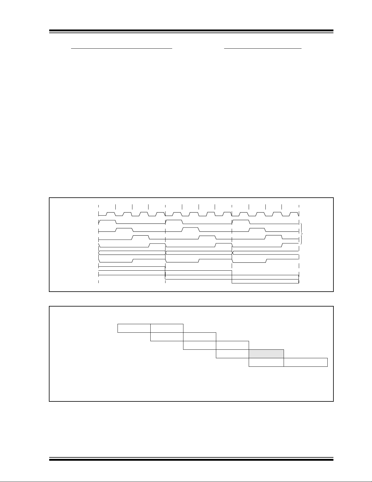
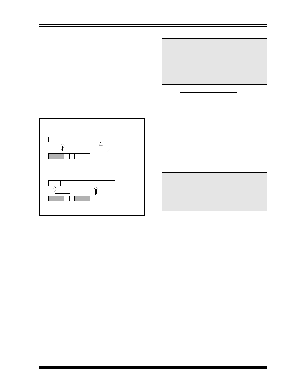
3.1 Clocking Scheme/Instruction Cycle
The clock input (from OSC1) is internally divided by
four to generate four non-overlapping quadrature
clocks namely Q1, Q2, Q3 and Q4. Internally, the program counter (PC) is incremented every Q1, the
instruction is fetched from the program memory and
latched into the instruction register in Q4. The instruction is decoded and executed during the following Q1
through Q4. The clocks and instruction execution flow
is shown in Figure 3-3.
FIGURE 3-3: CLOCK/INSTRUCTION CYCLE
Q2 Q3 Q4
OSC1
Q1
Q2
Q3
Q4
PC
OSC2/CLKOUT
(RC mode)
Q1
PC PC+1 PC+2
Fetch INST (PC)
Execute INST (PC-1) Fetch INST (PC+1)
Q1
3.2 Instruction Flow/Pipelining
An “Instruction Cycle” consists of four Q cycles (Q1,
Q2, Q3 and Q4). The instruction fetch and execute are
pipelined such that fetch takes one instruction cycle
while decode and execute takes another instruction
cycle. However, due to the pipelining, each instruction
effectively executes in one cycle. If an instruction
causes the program counter to change (e.g. GOTO)
then two cycles are required to complete the instruction
(Example 3-1).
A fetch cycle begins with the program counter (PC)
incrementing in Q1.
In the execution cycle , the fetched instruction is latched
into the “Instruction Register" in cycle Q1. This instruction is then decoded and executed during the Q2, Q3,
and Q4 cycles. Data memory is read during Q2 (operand read) and written during Q4 (destination write).
Q2 Q3 Q4
Execute INST (PC) Fetch INST (PC+2)
Q2 Q3 Q4
Q1
Execute INST (PC+1)
Internal
phase
clock
EXAMPLE 3-1: INSTRUCTION PIPELINE FLOW
Tcy0 Tcy1 Tcy2 Tcy3 Tcy4 Tcy5
1. MOVLW 55h
2. MOVWF PORTB
3. CALL SUB_1
4. BSF PORTA, BIT3 (Forced NOP)
5. Instruction @ address SUB_1
All instructions are single cycle, except for any program branches. These take two cycles since the fetch
instruction is “flushed” from the pipeline while the new instruction is being fetched and then executed.
1997 Microchip Technology Inc. DS30444E - page 15
Fetch 1 Execute 1
Fetch 2 Execute 2
Fetch 3 Execute 3
Fetch 4 Flush
Fetch SUB_1 Execute SUB_1

PIC16C9XX
NOTES:
DS30444E - page 16 1997 Microchip Technology Inc.
PIC16C9XX
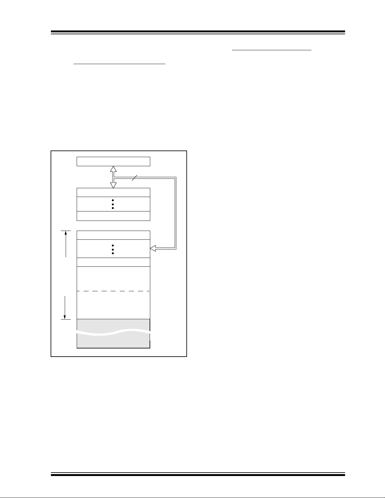
4.0 MEMORY ORGANIZATION
4.1 Program Memory Organization
The PIC16C9XX family has a 13-bit program counter
capable of addressing an 8K x 14 program memory
space.
Only the first 4K x 14 (0000h-0FFFh) is physically
implemented. Accessing a location above the physically implemented addresses will cause a wraparound.
The reset vector is at 0000h and the interrupt vector is
at 0004h.
FIGURE 4-1: PROGRAM MEMORY MAP
AND STACK
PC<12:0>
CALL, RETURN
RETFIE, RETLW
Interrupt Vector
On-chip Program
Space
User Memory
Memory (Page 0)
On-chip Program
Memory (Page 1)
Stack Level 1
Stack Level 8
Reset Vector
13
0000h
0004h
0005h
07FFh
0800h
4.2 Data Memory Organization
The data memory is partitioned into four Banks which
contain the General Purpose Registers and the Special
Function Registers. Bits RP1 and RP0 are the bank
select bits.
RP1:RP0 (STATUS<6:5>)
11 = Bank 3 (180h-1FFh)
10 = Bank 2 (100h-17Fh)
01 = Bank 1 (80h-FFh)
00 = Bank 0 (00h-7Fh)
The lower locations of each Bank are reserved for the
Special Function Registers. Above the Special Function Registers are General Purpose Registers implemented as static RAM. All four banks contain special
function registers. Some “high use” special function
registers are mirrored in other banks for code reduction
and quicker access.
4.2.1 GENERAL PURPOSE REGISTER FILE
The register file can be accessed either directly , or indi-
rectly through the File Select Register FSR
(Section 4.5).
The following General Purpose Registers are not physically implemented:
• F0h-FFh of Bank 1
• 170h-17Fh of Bank 2
• 1F0h-1FFh of Bank 3
These locations are used for common access across
banks.
0FFFh
1000h
1FFFh
1997 Microchip Technology Inc. DS30444E - page 17
PIC16C9XX
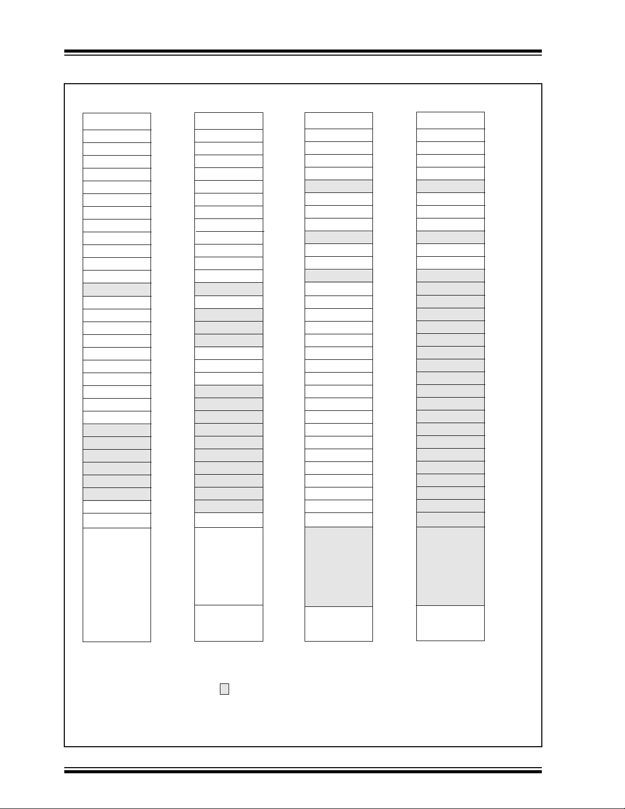
FIGURE 4-2: REGISTER FILE MAP
File
Address
Indirect addr.
TMR0
PCL
STATUS
FSR
PORTA
PORTB
PORTC
PORTD
PORTE
PCLATH
INTCON
PIR1
TMR1L
TMR1H
T1CON
TMR2
T2CON
SSPBUF
SSPCON
CCPR1L
CCPR1H
CCP1CON
ADRES
(2)
ADCON0
(2)
(1)
00h
01h
02h
03h
04h
05h
06h
07h
08h
09h
0Ah
0Bh
0Ch
0Dh
0Eh
0Fh
10h
11h
12h
13h
14h
15h
16h
17h
18h
19h
1Ah
1Bh
1Ch
1Dh
1Eh
1Fh
20h
Indirect addr.
OPTION
PCL
STATUS
FSR
TRISA
TRISB
TRISC
TRISD
TRISE
PCLATH
INTCON
PIE1
PCON
PR2
SSPADD
SSPSTAT
ADCON1
(2)
(1)
File
Address
80h
81h
82h
83h
84h
85h
86h
87h
88h
89h
8Ah
8Bh
8Ch
8Dh
8Eh
8Fh
90h
91h
92h
93h
94h
95h
96h
97h
98h
99h
9Ah
9Bh
9Ch
9Dh
9Eh
9Fh
A0h
Indirect addr.
TMR0
PCL
STATUS
FSR
PORTB
PORTF
PORTG
PCLATH
INTCON
LCDSE
LCDPS
LCDCON
LCDD00
LCDD01
LCDD02
LCDD03
LCDD04
LCDD05
LCDD06
LCDD07
LCDD08
LCDD09
LCDD10
LCDD11
LCDD12
LCDD13
LCDD14
LCDD15
(1)
File
Address
100h
101h
102h
103h
104h
105h
106h
107h
108h
109h
10Ah
10Bh
10Ch
10Dh
10Eh
10Fh
110h
111h
112h
113h
114h
115h
116h
117h
118h
119h
11Ah
11Bh
11Ch
11Dh
11Eh
11Fh
120h
Indirect addr.
OPTION
PCL
STATUS
FSR
TRISB
TRISF
TRISG
PCLATH
INTCON
Address
(1)
File
180h
181h
182h
183h
184h
185h
186h
187h
188h
189h
18Ah
18Bh
18Ch
18Dh
18Eh
18Fh
190h
191h
192h
193h
194h
195h
196h
197h
198h
199h
19Ah
19Bh
19Ch
19Dh
19Eh
19Fh
1A0h
General
Purpose
General
Register
Purpose
Register
Mapped in
Bank 0
Bank 0
7Fh
DS30444E - page 18 1997 Microchip Technology Inc.
70h-7Fh
Bank 1
Unimplemented data memory locations, read as '0'.
Note 1: Not a physical register.
2: These registers are not implemented on the PIC16C923.
EFh
F0h
FFh
Mapped in
Bank 0
70h-7Fh
Bank 2
16F
170
17F
Mapped in
Bank 0
70h-7Fh
Bank 3
1EFh
1F0h
1FFh
PIC16C9XX
4.2.2 SPECIAL FUNCTION REGISTERS
The special function registers can be classified into two
sets (core and peripheral). Those registers associated
The Special Function Registers are registers used by
the CPU and Peripheral Modules for controlling the
desired operation of the device. These registers are
implemented as static RAM.
with the “core” functions are described in this section,
and those related to the operation of the peripheral features are described in the section of that peripheral feature.
T ABLE 4-1: SPECIAL FUNCTION REGISTER SUMMARY
Address Name Bit 7 Bit 6 Bit 5 Bit 4 Bit 3 Bit 2 Bit 1 Bit 0
Value on
Power-on
Reset
Bank 0
00h INDF Addressing this location uses contents of FSR to address data memory (not a physical register) 0000 0000 0000 0000
01h TMR0 Timer0 module’s register xxxx xxxx uuuu uuuu
02h PCL Program Counter's (PC) Least Significant Byte 0000 0000 0000 0000
03h STATUS IRP RP1 RP0 T
04h FSR Indirect data memory address pointer xxxx xxxx uuuu uuuu
05h PORTA
06h PORTB PORTB Data Latch when written: PORTB pins when read xxxx xxxx uuuu uuuu
07h PORTC
08h PORTD PORTD Data Latch when written: PORTD pins when read 0000 0000 0000 0000
09h PORTE PORTE pins when read 0000 0000 0000 0000
0Ah PCLATH
0Bh INTCON GIE PEIE T0IE INTE RBIE T0IF INTF RBIF 0000 000x 0000 000u
0Ch PIR1 LCDIF ADIF
0Dh — Unimplemented — —
0Eh TMR1L Holding register for the Least Significant Byte of the 16-bit TMR1 register xxxx xxxx uuuu uuuu
0Fh TMR1H Holding register for the Most Significant Byte of the 16-bit TMR1 register xxxx xxxx uuuu uuuu
10h T1CON
11h TMR2 Timer2 module’s register 0000 0000 0000 0000
12h T2CON
13h SSPBUF Synchronous Serial Port Receive Buffer/Transmit Register xxxx xxxx uuuu uuuu
14h SSPCON WCOL SSPOV SSPEN CKP SSPM3 SSPM2 SSPM1 SSPM0 0000 0000 0000 0000
15h CCPR1L Capture/Compare/PWM Register (LSB) xxxx xxxx uuuu uuuu
16h CCPR1H Capture/Compare/PWM Register (MSB) xxxx xxxx uuuu uuuu
17h CCP1CON
18h — Unimplemented — —
19h — Unimplemented — —
1Ah — Unimplemented — —
1Bh — Unimplemented — —
1Ch — Unimplemented — —
1Dh — Unimplemented — —
(1)
1Eh
1Fh
Legend: x = unknown, u = unchanged, q = value depends on condition, - = unimplemented read as '0',
Note 1: Registers ADRES, ADCON0, and ADCON1 are not implemented in the PIC16C923, read as '0'.
ADRES A/D Result Register xxxx xxxx uuuu uuuu
(1)
ADCON0 ADCS1 ADCS0 CHS2 CHS1 CHS0 GO/DONE
shaded locations are unimplemented, read as ‘0’.
2: These bits are reserved on the PIC16C923, always maintain these bits clear.
3: These pixels do not display, but can be used as general purpose RAM.
4: PIC16C923 reset values for PORTA: --xx xxxx for a POR, and --uu uuuu for all other resets,
PIC16C924 reset values for PORTA: --0x 0000 when read.
5: Bit1 of ADCON0 is reserved on the PIC16C924, always maintain this bit clear.
— — PORTA Data Latch when written: PORTA pins when read
— — PORTC Data Latch when written: PORTC pins when read --xx xxxx --uu uuuu
— — — Write Buffer for the upper 5 bits of the Program Counter ---0 0000 ---0 0000
(2)
— — T1CKPS1 T1CKPS0 T1OSCEN T1SYNC TMR1CS TMR1ON --00 0000 --uu uuuu
— TOUTPS3 TOUTPS2 TOUTPS1 TOUTPS0 TMR2ON T2CKPS1 T2CKPS0 -000 0000 -000 0000
— — CCP1X CCP1Y CCP1M3 CCP1M2 CCP1M1 CCP1M0 --00 0000 --00 0000
— — SSPIF CCP1IF TMR2IF TMR1IF 00-- 0000 00-- 0000
O PD Z DC C 0001 1xxx 000q quuu
(4) (4)
(5)
ADON 0000 0000 0000 0000
Value on all
other resets
1997 Microchip Technology Inc. DS30444E - page 19
PIC16C9XX
TABLE 4-1: SPECIAL FUNCTION REGISTER SUMMARY (Cont.’d)
Address Name Bit 7 Bit 6 Bit 5 Bit 4 Bit 3 Bit 2 Bit 1 Bit 0
Bank 1
80h INDF Addressing this location uses contents of FSR to address data memory (not a physical register) 0000 0000 0000 0000
81h OPTION RBPU
82h PCL Program Counter's (PC) Least Significant Byte 0000 0000 0000 0000
83h STATUS IRP RP1 RP0 T
84h FSR Indirect data memory address pointer xxxx xxxx uuuu uuuu
85h TRISA
86h TRISB PORTB Data Direction Register 1111 1111 1111 1111
87h TRISC
88h TRISD PORTD Data Direction Register 1111 1111 1111 1111
89h TRISE PORTE Data Direction Register 1111 1111 1111 1111
8Ah PCLATH
8Bh INTCON GIE PEIE T0IE INTE RBIE T0IF INTF RBIF 0000 000x 0000 000u
8Ch PIE1 LCDIE ADIE
8Dh — Unimplemented — —
8Eh PCON
8Fh — Unimplemented — —
90h — Unimplemented — —
91h — Unimplemented — —
92h PR2 Timer2 Period Register 1111 1111 1111 1111
93h SSPADD Synchronous Serial Port (I
94h SSPSTAT SMP CKE D/A
95h — Unimplemented — —
96h — Unimplemented — —
97h — Unimplemented — —
98h — Unimplemented — —
99h — Unimplemented — —
9Ah — Unimplemented — —
9Bh — Unimplemented — —
9Ch — Unimplemented — —
9Dh — Unimplemented — —
9Eh — Unimplemented — —
(1)
9Fh
Legend: x = unknown, u = unchanged, q = value depends on condition, - = unimplemented read as '0',
Note 1: Registers ADRES, ADCON0, and ADCON1 are not implemented in the PIC16C923, read as '0'.
ADCON1 — — — — — PCFG2 PCFG1 PCFG0 ---- -000 ---- -000
shaded locations are unimplemented, read as ‘0’.
2: These bits are reserved on the PIC16C923, always maintain these bits clear.
3: These pixels do not display, but can be used as general purpose RAM.
4: PIC16C923 reset values for PORTA: --xx xxxx for a POR, and --uu uuuu for all other resets,
PIC16C924 reset values for PORTA: --0x 0000 when read.
5: Bit1 of ADCON0 is reserved on the PIC16C924, always maintain this bit clear.
INTEDG T0CS T0SE PSA PS2 PS1 PS0 1111 1111 1111 1111
O PD Z DC C 0001 1xxx 000q quuu
— — PORTA Data Direction Register --11 1111 --11 1111
— — PORTC Data Direction Register --11 1111 --11 1111
— — — Write Buffer for the upper 5 bits of the PC ---0 0000 ---0 0000
(2)
— — — — — — POR — ---- --0- ---- --u-
— — SSPIE CCP1IE TMR2IE TMR1IE 00-- 0000 00-- 0000
2
C mode) Address Register 0000 0000 0000 0000
P S R/W UA BF 0000 0000 0000 0000
Value on
Power-on
Reset
Value on all
other resets
DS30444E - page 20 1997 Microchip Technology Inc.
PIC16C9XX
TABLE 4-1: SPECIAL FUNCTION REGISTER SUMMARY (Cont.’d)
Address Name Bit 7 Bit 6 Bit 5 Bit 4 Bit 3 Bit 2 Bit 1 Bit 0
Bank 2
100h INDF Addressing this location uses contents of FSR to address data memory (not a physical register) 0000 0000 0000 0000
101h TMR0 Timer0 module’s register xxxx xxxx uuuu uuuu
102h PCL Program Counter's (PC) Least Significant Byte 0000 0000 0000 0000
103h STATUS IRP RP1 RP0 T
104h FSR Indirect data memory address pointer xxxx xxxx uuuu uuuu
105h — Unimplemented — —
106h PORTB PORTB Data Latch when written: PORTB pins when read xxxx xxxx uuuu uuuu
107h PORTF PORTF pins when read 0000 0000 0000 0000
108h PORTG PORTG pins when read 0000 0000 0000 0000
109h — Unimplemented — —
10Ah PCLATH
10Bh INTCON GIE PEIE T0IE INTE RBIE T0IF INTF RBIF 0000 000x 0000 000u
10Ch — Unimplemented — —
10Dh LCDSE SE29 SE27 SE20 SE16 SE12 SE9 SE5 SE0 1111 1111 1111 1111
10Eh LCDPS
10Fh LCDCON LCDEN SLPEN
110h LCDD00
111h LCDD01
112h LCDD02
113h LCDD03
114h LCDD04
115h LCDD05
116h LCDD06
117h LCDD07
118h LCDD08
119h LCDD09
11Ah LCDD10
11Bh LCDD11
11Ch LCDD12
11Dh LCDD13
11Eh LCDD14
11Fh LCDD15
Legend: x = unknown, u = unchanged, q = value depends on condition, - = unimplemented read as '0',
shaded locations are unimplemented, read as ‘0’.
Note 1: Registers ADRES, ADCON0, and ADCON1 are not implemented in the PIC16C923, read as '0'.
2: These bits are reserved on the PIC16C923, always maintain these bits clear.
3: These pixels do not display, but can be used as general purpose RAM.
4: PIC16C923 reset values for PORTA: --xx xxxx for a POR, and --uu uuuu for all other resets,
PIC16C924 reset values for PORTA: --0x 0000 when read.
5: Bit1 of ADCON0 is reserved on the PIC16C924, always maintain this bit clear.
— — — Write Buffer for the upper 5 bits of the PC ---0 0000 ---0 0000
— — — — LP3 LP2 LP1 LP0 ---- 0000 ---- 0000
— VGEN CS1 CS0 LMUX1 LMUX0 00-0 0000 00-0 0000
SEG07
COM0
SEG15
COM0
SEG23
COM0
SEG31
COM0
SEG07
COM1
SEG15
COM1
SEG23
COM1
SEG31
COM1
SEG07
COM2
SEG15
COM2
SEG23
COM2
SEG31
COM2
SEG07
COM3
SEG15
COM3
SEG23
COM3
SEG31
COM3
SEG06
COM0
SEG14
COM0
SEG22
COM0
SEG30
COM0
SEG06
COM1
SEG14
COM1
SEG22
COM1
SEG30
(3)
COM1
SEG06
COM2
SEG14
COM2
SEG22
COM2
SEG30
(3)
COM2
SEG06
COM3
SEG14
COM3
SEG22
COM3
SEG30
(3)
COM3
SEG05
COM0
SEG13
COM0
SEG21
COM0
SEG29
COM0
SEG05
COM1
SEG13
COM1
SEG21
COM1
SEG29
COM1
SEG05
COM2
SEG13
COM2
SEG21
COM2
SEG29
(3)
COM2
SEG05
COM3
SEG13
COM3
SEG21
COM3
SEG29
(3)
COM3
(3)
O PD Z DC C 0001 1xxx 000q quuu
SEG04
COM0
SEG12
COM0
SEG20
COM0
SEG28
COM0
SEG04
COM1
SEG12
COM1
SEG20
COM1
SEG28
COM1
SEG04
COM2
SEG12
COM2
SEG20
COM2
SEG28
COM2
SEG04
COM3
SEG12
COM3
SEG20
COM3
SEG28
COM3
SEG03
COM0
SEG11
COM0
SEG19
COM0
SEG27
COM0
SEG03
COM1
SEG11
COM1
SEG19
COM1
SEG27
COM1
SEG03
COM2
SEG11
COM2
SEG19
COM2
SEG27
COM2
SEG03
COM3
SEG11
COM3
SEG19
COM3
SEG27
COM3
SEG02
COM0
SEG10
COM0
SEG18
COM0
SEG26
COM0
SEG02
COM1
SEG10
COM1
SEG18
COM1
SEG26
COM1
SEG02
COM2
SEG10
COM2
SEG18
COM2
SEG26
COM2
SEG02
COM3
SEG10
COM3
SEG18
COM3
SEG26
COM3
SEG01
COM0
SEG09
COM0
SEG17
COM0
SEG25
COM0
SEG01
COM1
SEG09
COM1
SEG17
COM1
SEG25
COM1
SEG01
COM2
SEG09
COM2
SEG17
COM2
SEG25
COM2
SEG01
COM3
SEG09
COM3
SEG17
COM3
SEG25
COM3
SEG00
COM0
SEG08
COM0
SEG16
COM0
SEG24
COM0
SEG00
COM1
SEG08
COM1
SEG16
COM1
SEG24
COM1
SEG00
COM2
SEG08
COM2
SEG16
COM2
SEG24
COM2
SEG00
COM3
SEG08
COM3
SEG16
COM3
SEG24
COM3
Value on
Power-on
Reset
xxxx xxxx uuuu uuuu
xxxx xxxx uuuu uuuu
xxxx xxxx uuuu uuuu
xxxx xxxx uuuu uuuu
xxxx xxxx uuuu uuuu
xxxx xxxx uuuu uuuu
xxxx xxxx uuuu uuuu
xxxx xxxx uuuu uuuu
xxxx xxxx uuuu uuuu
xxxx xxxx uuuu uuuu
xxxx xxxx uuuu uuuu
xxxx xxxx uuuu uuuu
xxxx xxxx uuuu uuuu
xxxx xxxx uuuu uuuu
xxxx xxxx uuuu uuuu
xxxx xxxx uuuu uuuu
Value on all
other resets
1997 Microchip Technology Inc. DS30444E - page 21
PIC16C9XX
TABLE 4-1: SPECIAL FUNCTION REGISTER SUMMARY (Cont.’d)
Address Name Bit 7 Bit 6 Bit 5 Bit 4 Bit 3 Bit 2 Bit 1 Bit 0
Bank 3
180h INDF Addressing this location uses contents of FSR to address data memory (not a physical register) 0000 0000 0000 0000
181h OPTION RBPU
182h PCL Program Counter's (PC) Least Significant Byte 0000 0000 0000 0000
183h STATUS IRP RP1 RP0 T
184h FSR Indirect data memory address pointer xxxx xxxx uuuu uuuu
185h — Unimplemented — —
186h TRISB PORTB Data Direction Register 1111 1111 1111 1111
187h TRISF PORTF Data Direction Register 1111 1111 1111 1111
188h TRISG PORTG Data Direction Register 1111 1111 1111 1111
189h — Unimplemented — —
18Ah PCLATH
18Bh INTCON GIE PEIE T0IE INTE RBIE T0IF INTF RBIF 0000 000x 0000 000u
18Ch — Unimplemented — —
18Dh — Unimplemented — —
18Eh — Unimplemented — —
18Fh — Unimplemented — —
190h — Unimplemented — —
191h — Unimplemented — —
192h — Unimplemented — —
193h — Unimplemented — —
194h — Unimplemented — —
195h — Unimplemented — —
196h — Unimplemented — —
197h — Unimplemented — —
198h — Unimplemented — —
199h — Unimplemented — —
19Ah — Unimplemented — —
19Bh — Unimplemented — —
19Ch — Unimplemented — —
19Dh — Unimplemented — —
19Eh — Unimplemented — —
19Fh — Unimplemented — —
Legend: x = unknown, u = unchanged, q = value depends on condition, - = unimplemented read as '0',
shaded locations are unimplemented, read as ‘0’.
Note 1: Registers ADRES, ADCON0, and ADCON1 are not implemented in the PIC16C923, read as '0'.
2: These bits are reserved on the PIC16C923, always maintain these bits clear.
3: These pixels do not display, but can be used as general purpose RAM.
4: PIC16C923 reset values for PORTA: --xx xxxx for a POR, and --uu uuuu for all other resets,
PIC16C924 reset values for PORTA: --0x 0000 when read.
5: Bit1 of ADCON0 is reserved on the PIC16C924, always maintain this bit clear.
INTEDG T0CS T0SE PSA PS2 PS1 PS0 1111 1111 1111 1111
O PD Z DC C 0001 1xxx 000q quuu
— — — Write Buffer for the upper 5 bits of the PC ---0 0000 ---0 0000
Value on
Power-on
Reset
Value on all
other resets
DS30444E - page 22 1997 Microchip Technology Inc.
PIC16C9XX
4.2.2.1 STATUS REGISTER
The ST ATUS register, shown in Figure 4-3, contains the
arithmetic status of the ALU, the RESET status and the
bank select bits for data memory.
The STATUS register can be the destination for any
instruction, as with any other register. If the STATUS
register is the destination for an instruction that affects
the Z, DC or C bits, then the write to these three bits is
disabled. These bits are set or cleared according to the
device logic. Furthermore, the T
writable. Therefore, the result of an instruction with the
STATUS register as destination may be different than
intended.
For example, CLRF STATUS will clear the upper-three
bits and set the Z bit. This leaves the STATUS register
as 000u u1uu (where u = unchanged).
O and PD bits are not
It is recommended, therefore, that only BCF, BSF,
SWAPF and MOVWF instructions are used to alter the
STATUS register because these instructions do not
affect the Z, C or DC bits from the STA TUS register. For
other instructions, not affecting any status bits, see the
“Instruction Set Summary.”
Note 1: The C and DC bits operate as a borrow
and digit borrow bit, respectively, in subtraction. See the SUBLW and SUBWF
instructions for examples.
FIGURE 4-3: STATUS REGISTER (ADDRESS 03h, 83h, 103h, 183h)
R/W-0 R/W-0 R/W-0 R-1 R-1 R/W-x R/W-x R/W-x
IRP RP1 RP0 TO PD Z DC C R = Readable bit
bit7 bit0
bit 7: IRP: Register Bank Select bit (used for indirect addressing)
1 = Bank 2, 3 (100h - 1FFh)
0 = Bank 0, 1 (00h - FFh)
bit 6-5: RP1:RP0: Register Bank Select bits (used for direct addressing)
11 = Bank 3 (180h - 1FFh)
10 = Bank 2 (100h - 17Fh)
01 = Bank 1 (80h - FFh)
00 = Bank 0 (00h - 7Fh)
bit 4: T
bit 3: PD
bit 2: Z: Zero bit
bit 1: DC: Digit carry/borro
bit 0: C: Carry/borro
O: Time-out bit
1 = After power-up, CLRWDT instruction, or SLEEP instruction
0 = A WDT time-out occurred
: Power-down bit
1 = After power-up or by the CLRWDT instruction
0 = By execution of the SLEEP instruction
1 = The result of an arithmetic or logic operation is zero
0 = The result of an arithmetic or logic operation is not zero
w bit (ADDWF, ADDLW,SUBLW,SUBWF instructions) (for borrow the polarity is reversed)
1 = A carry-out from the 4th low order bit of the result occurred
0 = No carry-out from the 4th low order bit of the result
w bit (ADDWF, ADDLW,SUBLW,SUBWF instructions) (for borrow the polarity is reversed)
1 = A carry-out from the most significant bit of the result occurred
0 = No carry-out from the most significant bit of the result occurred
Note: A subtraction is executed by adding the two’s complement of the second operand. For rotate (RRF,
RLF) instructions, this bit is loaded with either the high or low order bit of the source register.
W = Writable bit
U = Unimplemented bit,
read as ‘0’
- n = Value at POR reset
1997 Microchip Technology Inc. DS30444E - page 23

PIC16C9XX
4.2.2.2 OPTION REGISTER
Note: To achieve a 1:1 prescaler assignment for
The OPTION register is a readable and writable register which contains various control bits to configure the
the TMR0 register, assign the prescaler to
the Watchdog Timer.
TMR0/WDT prescaler, the external RB0/INT pin interrupt, TMR0, and the weak pull-ups on PORTB.
FIGURE 4-4: OPTION REGISTER (ADDRESS 81h, 181h)
R/W-1 R/W-1 R/W-1 R/W-1 R/W-1 R/W-1 R/W-1 R/W-1
RBPU INTEDG T0CS T0SE PSA PS2 PS1 PS0 R = Readable bit
bit7 bit0
bit 7: RBPU: PORTB Pull-up Enable bit
1 = PORTB pull-ups are disabled
0 = PORTB pull-ups are enabled by individual port latch values
bit 6: INTEDG: Interrupt Edge Select bit
1 = Interrupt on rising edge of RB0/INT pin
0 = Interrupt on falling edge of RB0/INT pin
bit 5: T0CS: TMR0 Clock Source Select bit
1 = Transition on RA4/T0CKI pin
0 = Internal instruction cycle clock (CLKOUT)
bit 4: T0SE: TMR0 Source Edge Select bit
1 = Increment on high-to-low transition on RA4/T0CKI pin
0 = Increment on low-to-high transition on RA4/T0CKI pin
bit 3: PSA: Prescaler Assignment bit
1 = Prescaler is assigned to the WDT
0 = Prescaler is assigned to the Timer0 module
bit 2-0: PS2:PS0: Prescaler Rate Select bits
Bit Value TMR0 Rate WDT Rate
000
001
010
011
100
101
110
111
1 : 2
1 : 4
1 : 8
1 : 16
1 : 32
1 : 64
1 : 128
1 : 256
1 : 1
1 : 2
1 : 4
1 : 8
1 : 16
1 : 32
1 : 64
1 : 128
W = Writable bit
U = Unimplemented bit,
read as ‘0’
- n = Value at POR reset
DS30444E - page 24 1997 Microchip Technology Inc.

PIC16C9XX
4.2.2.3 INTCON REGISTER
The INTCON Register is a readable and writable regis-
ter which contains various enable and flag bits for the
TMR0 register overflow, RB Port change and external
RB0/INT pin interrupts.
Note: Interrupt flag bits get set when an interrupt
condition occurs regardless of the state of
its corresponding enable bit or the global
enable bit, GIE (INTCON<7>).
FIGURE 4-5: INTCON REGISTER (ADDRESS 0Bh, 8Bh, 10Bh, 18Bh)
R/W-0 R/W-0 R/W-0 R/W-0 R/W-0 R/W-0 R/W-0 R/W-x
GIE PEIE T0IE INTE RBIE T0IF INTF RBIF R = Readable bit
bit7 bit0
bit 7: GIE: Global Interrupt Enable bit
1 = Enables all un-masked interrupts
0 = Disables all interrupts
bit 6: PEIE: Peripheral Interrupt Enable bit
1 = Enables all un-masked peripheral interrupts
0 = Disables all peripheral interrupts
bit 5: T0IE: TMR0 Overflow Interrupt Enable bit
1 = Enables the TMR0 interrupt
0 = Disables the TMR0 interrupt
bit 4: INTE: RB0/INT External Interrupt Enable bit
1 = Enables the RB0/INT external interrupt
0 = Disables the RB0/INT external interrupt
bit 3: RBIE: RB Port Change Interrupt Enable bit
1 = Enables the RB port change interrupt
0 = Disables the RB port change interrupt
bit 2: T0IF: TMR0 Overflow Interrupt Flag bit
1 = TMR0 register has overflowed (must be cleared in software)
0 = TMR0 register did not overflow
bit 1: INTF: RB0/INT External Interrupt Flag bit
1 = The RB0/INT external interrupt occurred (must be cleared in software)
0 = The RB0/INT external interrupt did not occur
bit 0: RBIF: RB Port Change Interrupt Flag bit
1 = At least one of the RB7:RB4 pins changed state (see Section 5.2 to clear interrupt)
0 = None of the RB7:RB4 pins have changed state
Interrupt flag bits get set when an interrupt condition occurs regardless of the state of its corresponding enable bit or the
global enable bit, GIE (INTCON<7>). User software should ensure the appropriate interrupt flag bits are clear prior to
enabling an interrupt.
W = Writable bit
U = Unimplemented bit,
read as ‘0’
- n = Value at POR reset
1997 Microchip Technology Inc. DS30444E - page 25
PIC16C9XX
4.2.2.4 PIE1 REGISTER
Note: Bit PEIE (INTCON<6>) must be set to
This register contains the individual enable bits for the
enable any peripheral interrupt.
peripheral interrupts.
FIGURE 4-6: PIE1 REGISTER (ADDRESS 8Ch)
R/W-0 R/W-0 U-0 U-0 R/W-0 R/W-0 R/W-0 R/W-0
LCDIE ADIE
bit7 bit0
bit 7: LCDIE: LCD Interrupt Enable bit
bit 6: ADIE: A/D Converter Interrupt Enable bit
bit 5-4: Unimplemented: Read as '0'
bit 3: SSPIE: Synchronous Serial Port Interrupt Enable bit
bit 2: CCP1IE: CCP1 Interrupt Enable bit
bit 1: TMR2IE: TMR2 to PR2 Match Interrupt Enable bit
bit 0: TMR1IE: TMR1 Overflow Interrupt Enable bit
Note 1: Bit ADIE is reserved on the PIC16C923, always maintain this bit clear.
(1)
— — SSPIE CCP1IE TMR2IE TMR1IE R = Readable bit
1 = Enables the LCD interrupt
0 = Disables the LCD interrupt
(1)
1 = Enables the A/D interrupt
0 = Disables the A/D interrupt
1 = Enables the SSP interrupt
0 = Disables the SSP interrupt
1 = Enables the CCP1 interrupt
0 = Disables the CCP1 interrupt
1 = Enables the TMR2 to PR2 match interrupt
0 = Disables the TMR2 to PR2 match interrupt
1 = Enables the TMR1 overflow interrupt
0 = Disables the TMR1 overflow interrupt
W = Writable bit
U = Unimplemented bit,
read as ‘0’
- n = Value at POR reset
DS30444E - page 26 1997 Microchip Technology Inc.
PIC16C9XX
4.2.2.5 PIR1 REGISTER
This register contains the individual flag bits for the
peripheral interrupts.
Note: Interrupt flag bits get set when an interrupt
condition occurs regardless of the state of
its corresponding enable bit or the global
enable bit, GIE (INTCON<7>). User software should ensure the appropriate interrupt flag bits are clear prior to enabling an
interrupt.
FIGURE 4-7: PIR1 REGISTER (ADDRESS 0Ch)
R/W-0 R/W-0 U-0 U-0 R/W-0 R/W-0 R/W-0 R/W-0
LCDIF ADIF
bit7 bit0
bit 7: LCDIF: LCD Interrupt Flag bit
bit 6: ADIF: A/D Converter Interrupt Flag bit
bit 5-4: Unimplemented: Read as '0'
bit 3: SSPIF: Synchronous Serial Port Interrupt Flag bit
bit 2: CCP1IF: CCP1 Interrupt Flag bit
bit 1: TMR2IF: TMR2 to PR2 Match Interrupt Flag bit
bit 0: TMR1IF: TMR1 Overflow Interrupt Flag bit
Note 1: Bit ADIF is reserved on the PIC16C923, always maintain this bit clear.
Interrupt flag bits get set when an interrupt condition occurs regardless of the state of its corresponding enable bit or the
global enable bit, GIE (INTCON<7>). User software should ensure the appropriate interrupt flag bits are clear prior to
enabling an interrupt.
(1)
— — SSPIF CCP1IF TMR2IF TMR1IF R = Readable bit
W = Writable bit
U = Unimplemented bit,
- n = Value at POR reset
1 = LCD interrupt occurred (must be cleared in software)
0 = LCD interrupt did not occur
(1)
1 = An A/D conversion completed (must be cleared in software)
0 = The A/D conversion is not complete
1 = The transmission/reception is complete (must be cleared in software)
0 = Waiting to transmit/receive
Capture Mode
1 = A TMR1 register capture occurred (must be cleared in software)
0 = No TMR1 register capture occurred
Compare Mode
1 = A TMR1 register compare match occurred (must be cleared in software)
0 = No TMR1 register compare match occurred
PWM Mode
Unused in this mode
1 = TMR2 to PR2 match occurred (must be cleared in software)
0 = No TMR2 to PR2 match occurred
1 = TMR1 register overflowed (must be cleared in software)
0 = TMR1 register did not overflow
read as ‘0’
1997 Microchip Technology Inc. DS30444E - page 27
PIC16C9XX
4.2.2.6 PCON REGISTER
The Power Control (PCON) register contains a flag bit
to allow differentiation between a Power-on Reset
(POR) to an external MCLR
Reset or WDT Reset.
For various reset conditions see Table 14-4 and
Table 14-5.
FIGURE 4-8: PCON REGISTER (ADDRESS 8Eh)
U-0 U-0 U-0 U-0 U-0 U-0 R/W-0 U-0
— — — — — — POR — R = Readable bit
bit7 bit0
bit 7-2: Unimplemented: Read as '0'
bit 1: POR
bit 0: Unimplemented: Read as '0'
: Power-on Reset Status bit
1 = No Power-on Reset occurred
0 = A Power-on Reset occurred (must be set in software after a Power-on Reset occurs)
W = Writable bit
U = Unimplemented bit,
- n = Value at POR reset
read as ‘0’
DS30444E - page 28 1997 Microchip Technology Inc.
4.3 PCL and PCLATH
The program counter (PC) is 13-bits wide. The lo w byte
comes from the PCL register, which is a readable and
writable register. The upper bits (PC<12:8>) are not
readable, but are indirectly writable through the
PCLATH register. On an y reset, the upper bits of the PC
will be cleared. Figure 4-9 sho ws the two situations for
the loading of the PC. The upper example in the figure
shows how the PC is loaded on a write to PCL
(PCLATH<4:0> → PCH). The lower example in the fig-
ure shows how the PC is loaded during a CALL or GOTO
instruction (PCLATH<4:3> → PCH).
FIGURE 4-9: LOADING OF PC IN
DIFFERENT SITUATIONS
PCH PCL
12 8 7 0
PC
PCLATH<4:0>
5
PCLATH
PCH PCL
12 11 10 0
PC
2
8 7
PCLATH<4:3>
PCLATH
11
8
Instr
uction with
PCL as
Destination
ALU result
GOTO, CALL
Opcode <10:0>
PIC16C9XX
Note 1: There are no status bits to indicate stack
overflow or stack underflow conditions.
Note 2: There are no instructions/mnemonics
called PUSH or POP. These are actions
that occur from the execution of the
CALL, RETURN, RETLW, and RETFIE
instructions, or the vectoring to an interrupt address.
4.4 Program Memory Paging
PIC16C9XX devices are capable of addressing a continuous 8K word block of program memory. The CALL
and GOTO instructions provide only 11 bits of address
to allow branching within any 2K program memory
page. When doing a CALL or GOTO instruction the
upper 2 bits of the address are provided by
PCLATH<4:3>. When doing a CALL or GOTO instruction, the user must ensure that the page select bits are
programmed so that the desired program memory
page is addressed. If a return from a CALL instruction
(or interrupt) is executed, the entire 13-bit PC is pushed
onto the stack. Therefore, manipulation of the
PCLATH<4:3> bits are not required for the return
instructions (which POPs the address from the stack).
Note: The PIC16C9XX ignores paging bit
PCLATH<4>, which is used to access program memory pages 2 and 3. The use of
PCLATH<4> as a general purpose
read/write bit is not recommended since
this may affect upward compatibility with
future products.
4.3.1 COMPUTED GOTO
A computed GOT O is accomplished by adding an offset
to the program counter (ADDWF PCL). When doing a
table read using a computed GOTO method, care
should be exercised if the tab le location crosses a PCL
memory boundary (each 256 byte block). Refer to the
application note
“Implementing a Table Read”
(AN556).
4.3.2 STACK
The PIC16CXXX family has an 8 level deep x 13-bit
wide hardware stack. The stack space is not part of
either program or data space and the stack pointer is
not readable or writable. The PC is PUSHed onto the
stack when a CALL instruction is executed or an interrupt causes a branch. The stack is POPed in the event
of a RETURN, RETLW or a RETFIE instruction execution. PCLATH is not affected by a PUSH or POP operation.
The stack operates as a circular buff er . This means that
after the stack has been PUSHed eight times, the ninth
push overwrites the value that was stored from the first
push. The tenth push overwrites the second push (and
so on).
1997 Microchip Technology Inc. DS30444E - page 29
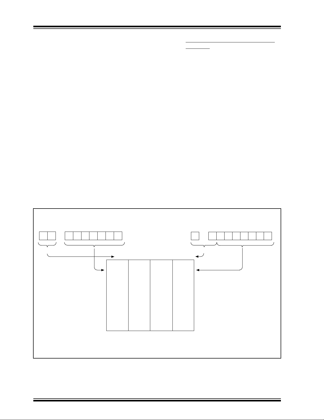
PIC16C9XX
Example 4-1 shows the calling of a subroutine in
page 1 of the program memory . This example assumes
that PCLA TH is sa ved and restored by the interrupt service routine (if interrupts are used).
EXAMPLE 4-1: CALL OF A SUBROUTINE IN
PAGE 1 FROM PAGE 0
ORG 0x500
BSF PCLATH,3 ;Select page 1 (800h-FFFh)
CALL SUB1_P1 ;Call subroutine in
: ;page 1 (800h-FFFh)
:
:
ORG 0x900
SUB1_P1: ;called subroutine
: ;page 1 (800h-FFFh)
:
RETURN ;return to Call subroutine
;in page 0 (000h-7FFh)
4.5 Indirect Addressing, INDF and FSR
Registers
The INDF register is not a physical register . Addressing
the INDF register will cause indirect addressing.
Indirect addressing is possible by using the INDF register. Any instruction using the INDF register actually
accesses the register pointed to by the File Select Register (FSR). Reading the INDF register itself indirectly
(FSR = '0') will produce 00h. Writing to the INDF register indirectly results in a no-operation (although status
bits may be affected). An effective 9-bit address is
obtained by concatenating the 8-bit FSR register and
the IRP bit (STATUS<7>), as shown in Figure 4-10.
A simple program to clear RAM locations 20h-2Fh
using indirect addressing is shown in Example 4-2.
EXAMPLE 4-2: INDIRECT ADDRESSING
movlw 0x20 ;initialize pointer
movwf FSR ;to RAM
NEXT clrf INDF ;clear INDF register
incf FSR,F ;inc pointer
btfss FSR,4 ;all done?
goto NEXT ;no clear next
CONTINUE
: ;yes continue
FIGURE 4-10: DIRECT/INDIRECT ADDRESSING
RP1:RP0 6
bank select location select
For memory map detail see Figure 4-2.
from opcode
Data
Memory
0
00 01 10 11
00h
7Fh
Bank 0 Bank 1 Bank 2 Bank 3
Indirect AddressingDirect Addressing
IRP FSR register
bank select
7
location select
00h
7Fh
0
DS30444E - page 30 1997 Microchip Technology Inc.
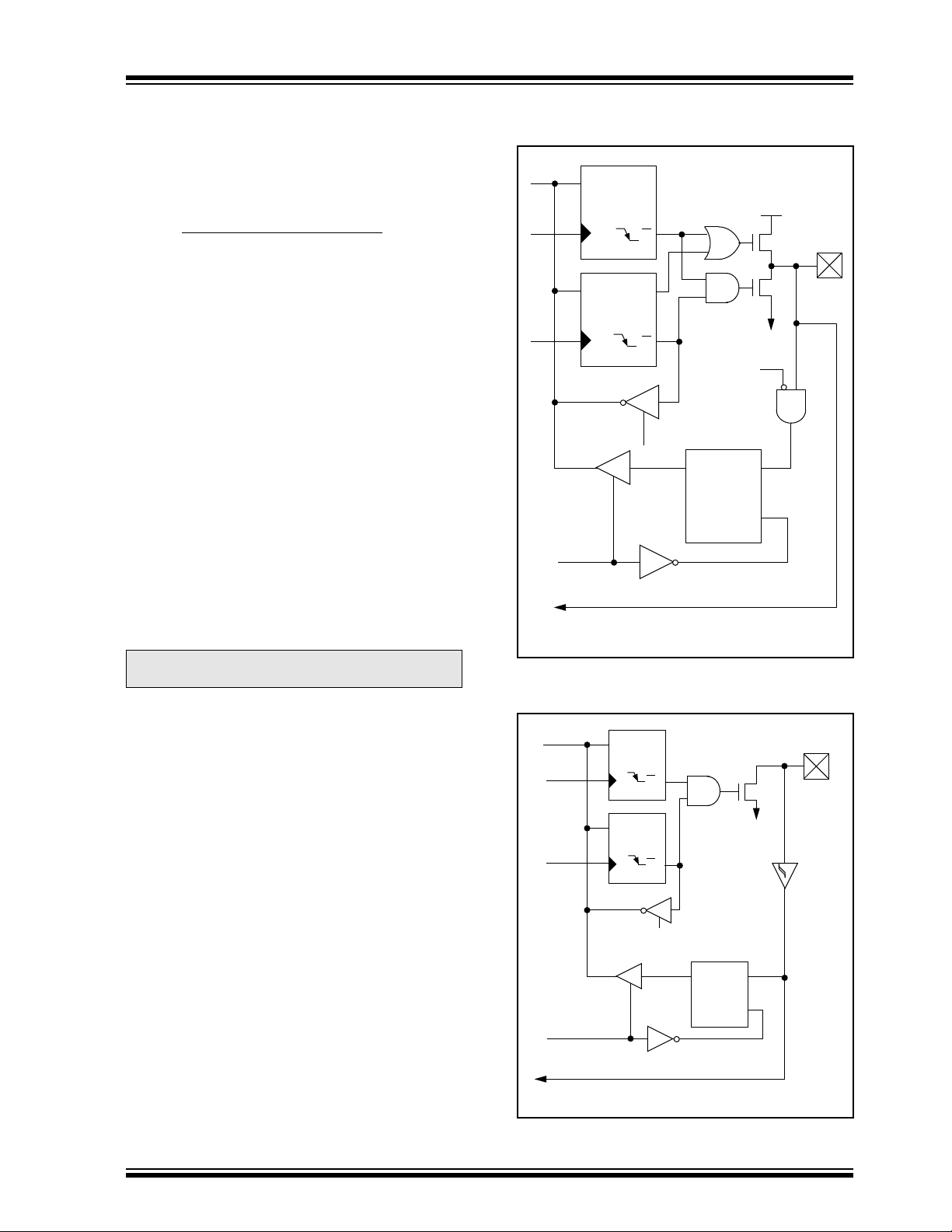
PIC16C9XX
5.0 PORTS
Some pins for these ports are multiplexed with an alternate function for the peripheral features on the device.
In general, when a peripheral is enabled, that pin may
not be used as a general purpose I/O pin.
5.1 PORTA and TRISA Register
The RA4/T0CKI pin is a Schmitt Trigger input and an
open drain output. All other RA port pins hav e TTL input
levels and full CMOS output drivers. All RA pins have
data direction bits (TRISA register) which can configure
these pins as output or input.
Setting a bit in the TRISA register puts the corresponding output driver in a hi-impedance mode. Clearing a bit
in the TRISA register puts the contents of the output
latch on the selected pin.
Reading the PORTA register reads the status of the
pins whereas writing to it will write to the port latch. All
write operations are read-modify-write operations.
Therefore, a write to a port implies that the port pins are
read, this value is modified, and then written to the port
data latch.
Pin RA4 is multiplexed with the Timer0 module clock
input to become the RA4/T0CKI pin.
For the PIC16C924 only, other PORTA pins are multiplexed with analog inputs and the analog V
The operation of each pin is selected by clearing/setting the control bits in the ADCON1 register (A/D Control Register1).
REF input.
FIGURE 5-1: BLOCK DIAGRAM OF PINS
RA3:RA0 AND RA5
Data
bus
WR
Port
WR
TRIS
RD PORT
To A/D Converter (PIC16C924 only)
Note 1: I/O pins have protection diodes to VDD and VSS.
CK
Data Latch
CK
TRIS Latch
QD
Q
QD
Q
RD TRIS
Analog
input
mode
Q D
EN
VDD
P
N
SS
V
I/O pin
TTL
input
buffer
(1)
Note: On a Power-on Reset, these pins are con-
figured as analog inputs and read as '0'.
The TRISA register controls the direction of the RA
pins, even when they are being used as analog inputs.
The user must ensure the bits in the TRISA register are
maintained set when using them as analog inputs.
EXAMPLE 5-1: INITIALIZING PORTA
BCF STATUS, RP0 ; Select Bank0
BCF STATUS, RP1
CLRF PORTA ; Initialize PORTA
BSF STATUS, RP0 ;
MOVLW 0xCF ; Value used to
; initialize data
; direction
MOVWF TRISA ; Set RA<3:0> as inputs
; RA<5:4> as outputs
; RA<7:6> are always
; read as '0'.
FIGURE 5-2: BLOCK DIAGRAM OF
RA4/T0CKI PIN
Data
bus
WR
PORT
WR
TRIS
RD PORT
TMR0 clock input
Note 1: I/O pin has protection diodes to V
QD
Q
CK
Data Latch
QD
Q
CK
TRIS Latch
RD TRIS
Schmitt
Trigger
input
buffer
Q D
EN
EN
N
V
SS
I/O pin
SS only.
(1)
1997 Microchip Technology Inc. DS30444E - page 31

PIC16C9XX
TABLE 5-1: PORTA FUNCTIONS
Name Bit# Buffer Function
RA0/AN0
RA1/AN1
RA2/AN2
(1)
(1)
(1)
RA3/AN3/V
RA4/T0CKI bit4 ST Input/output or external clock input for Timer0
RA5/AN4/SS
Legend: TTL = TTL input, ST = Schmitt Trigger input
Note 1: The AN and V
TABLE 5-2: SUMMARY OF REGISTERS ASSOCIATED WITH PORTA
bit0 TTL Input/output or analog input
bit1 TTL Input/output or analog input
bit2 TTL Input/output or analog input
(1)
REF
bit3 TTL Input/output or analog input or VREF
Output is open drain type
(1)
bit5 TTL Input/output or analog input or slave select input for synchronous serial port
REF functions are for the A/D module and are only implemented on the PIC16C924.
Value on
Address Name Bit 7 Bit 6 Bit 5 Bit 4 Bit 3 Bit 2 Bit 1 Bit 0
05h PORTA — — RA5 RA4 RA3 RA2 RA1 RA0 (2) (2)
85h TRISA — — PORTA Data Direction Control Register --11 1111 --11 1111
(1)
9Fh
Legend: x = unknown, u = unchanged, - = unimplemented locations read as '0'. Shaded cells are not used by PORTA.
Note 1: The ADCON1 register is implemented on the PIC16C924 only.
ADCON1 — — — — — PCFG2 PCFG1 PCFG0 ---- -000 ---- -000
2: PIC16C923 reset values for PORTA: --xx xxxx for a POR, and --uu uuuu for all other resets,
PIC16C924 reset values for PORTA: --0x 0000 when read.
Power-on
Reset
Value on
all other
resets
DS30444E - page 32 1997 Microchip Technology Inc.

PIC16C9XX
5.2 PORTB and TRISB Register
PORTB is an 8-bit wide bi-directional port. The corresponding data direction register is TRISB. Setting a bit
in the TRISB register puts the corresponding output
driver in a hi-impedance input mode. Clearing a bit in
the TRISB register puts the contents of the output latch
on the selected pin(s).
EXAMPLE 5-2: INITIALIZING PORTB
BCF STATUS, RP0 ; Select Bank0
BCF STATUS, RP1
CLRF PORTB ; Initialize PORTB
BSF STATUS, RP0 ;
MOVLW 0xCF ; Value used to
; initialize data
; direction
MOVWF TRISB ; Set RB<3:0> as inputs
; RB<5:4> as outputs
; RB<7:6> as inputs
Each of the PORTB pins has a weak internal pull-up. A
single control bit can turn on all the pull-ups. This is
performed by clearing bit RBPU
(OPTION<7>). The
weak pull-up is automatically turned off when the port
pin is configured as an output. The pull-ups are also disabled on a Power-on Reset.
FIGURE 5-3: BLOCK DIAGRAM OF
RB3:RB0 PINS
DD
TTL
Input
Buffer
EN
V
weak
P
pull-up
RD Port
I/O
pin
(1)
(2)
RBPU
Data bus
WR Port
WR TRIS
RB0/INT
Note 1: I/O pins have diode protection to V
2: To enable weak pull-ups, set the appropriate TRIS bit
and clear the RBPU
Data Latch
QD
CK
TRIS Latch
QD
CK
RD TRIS
RD Port
Schmitt Trigger
Buffer
bit (OPTION<7>).
Q D
DD and VSS.
Four of PORTB’s pins, RB7:RB4, have an interrupt on
change feature. Only pins configured as inputs can
cause this interrupt to occur (i.e. an y RB7:RB4 pin configured as an output is excluded from the interrupt on
change comparison). The input pins (of RB7:RB4) are
compared with the old value latched on the last read of
PORTB. The “mismatch” outputs of RB7:RB4 are
OR’ed together to generate the RB Port Change Interrupt with flag bit RBIF (INTCON<0>).
This interrupt can wake the device from SLEEP. The
user, in the interrupt service routine, can clear the interrupt in the following manner:
a) Any read or write of PORTB. This will end the
mismatch condition.
b) Clear flag bit RBIF.
A mismatch condition will continue to set flag bit RBIF.
Reading PORTB will end the mismatch condition, and
allow flag bit RBIF to be cleared.
This interrupt on mismatch feature, together with software configurable pull-ups on these four pins allow
easy interface to a keypad and make it possible for
wake-up on key-depression. Refer to the
Embedded
Control Handbook, "Implementing Wake-Up on Key
Stroke"
(AN552).
The interrupt on change feature is recommended for
wake-up on key depression operation and operations
where PORTB is only used for the interrupt on change
feature. Polling of PORTB is not recommended while
using the interrupt on change feature.
FIGURE 5-4: BLOCK DIAGRAM OF
RB7:RB4 PINS
DD
EN
EN
TTL
Input
Buffer
V
P
weak
pull-up
I/O
(1)
pin
ST
Buffer
Q1
RD Port
Q3
(2)
RBPU
Data bus
WR Port
WR TRIS
Set RBIF
From other
RB7:RB4 pins
RB7:RB6 in serial programming mode
Note 1: I/O pins have diode protection to VDD and VSS.
2: To enable weak pull-ups, set the appropriate TRIS bit
and clear the RBPU
Data Latch
QD
CK
TRIS Latch
QD
CK
RD TRIS
RD Port
bit (OPTION<7>).
Latch
Q D
Q D
1997 Microchip Technology Inc. DS30444E - page 33

PIC16C9XX
TABLE 5-3: PORTB FUNCTIONS
Name Bit# Buffer Function
RB0/INT bit0 TTL/ST Input/output pin or external interrupt input. Internal software
programmable weak pull-up. This buffer is a Schmitt Trigger input when
configured as the external interrupt.
RB1 bit1 TTL Input/output pin. Internal software programmable weak pull-up.
RB2 bit2 TTL Input/output pin. Internal software programmable weak pull-up.
RB3 bit3 TTL Input/output pin. Internal software programmable weak pull-up.
RB4 bit4 TTL Input/output pin (with interrupt on change). Internal software programmable
weak pull-up.
RB5 bit5 TTL Input/output pin (with interrupt on change). Internal software programmable
weak pull-up.
RB6 bit6 TTL/ST Input/output pin (with interrupt on change). Internal software programmable
weak pull-up. Serial programming clock. This buffer is a Schmitt Trigger
input when used in serial programming mode.
RB7 bit7 TTL/ST Input/output pin (with interrupt on change). Internal software programmable
weak pull-up. Serial progr amming data. This buffer is a Schmitt Trigger input
when used in serial programming mode.
Legend: TTL = TTL input, ST = Schmitt Trigger input
TABLE 5-4: SUMMARY OF REGISTERS ASSOCIATED WITH PORTB
Value on
Address Name Bit 7 Bit 6 Bit 5 Bit 4 Bit 3 Bit 2 Bit 1 Bit 0
06h, 106h PORTB RB7 RB6 RB5 RB4 RB3 RB2 RB1 RB0 xxxx xxxx uuuu uuuu
86h, 186h TRISB PORTB Data Direction Control Register 1111 1111 1111 1111
81h, 181h OPTION RBPU INTEDG T0CS T0SE PSA PS2 PS1 PS0 1111 1111 1111 1111
Legend: x = unknown, u = unchanged. Shaded cells are not used by PORTB.
Power-on
Reset
Value on all
other resets
DS30444E - page 34 1997 Microchip Technology Inc.

PIC16C9XX
5.3 PORTC and TRISC Register
PORTC is an 6-bit bi-directional port. Each pin is individually configurable as an input or output through the
TRISC register. PORTC is multiplexed with several
peripheral functions (Table 5-5). PORTC pins have
Schmitt Trigger input buffers.
When enabling peripheral functions, care should be
taken in defining TRIS bits for each PORTC pin. Some
peripherals override the TRIS bit to make a pin an output, while other peripherals override the TRIS bit to
make a pin an input. Since the TRIS bit override is in
effect while the peripheral is enabled, read-modify-write instructions (BSF, BCF, XORWF) with TRISC
as destination should be avoided. The user should ref er
to the corresponding peripheral section for the correct
TRIS bit settings.
EXAMPLE 5-3: INITIALIZING PORTC
BCF STATUS,RP0 ; Select Bank0
BCF STATUS,RP1
CLRF PORTC ; Initialize PORTC
BSF STATUS,RP0 ;
MOVLW 0xCF ; Value used to
; initialize data
; direction
MOVWF TRISC ; Set RC<3:0> as inputs
; RC<5:4> as outputs
; RC<7:6> always read 0
FIGURE 5-5: PORTC BLOCK DIAGRAM
(PERIPHERAL OUTPUT
OVERRIDE)
DD
TTL
Input
Buffer
EN
V
P
RD Port
(2)
RBPU
Data bus
WR Port
WR TRIS
RB0/INT
Note 1: I/O pins have diode protection to V
2: To enable weak pull-ups, set the appropriate TRIS bit(s)
and clear the RBPU bit (OPTION<7>).
Data Latch
CK
TRIS Latch
CK
RD TRIS
RD Port
Schmitt Trigger
Buffer
QD
QD
Q D
DD and VSS.
weak
pull-up
I/O
pin
(1)
TABLE 5-5: PORTC FUNCTIONS
Name Bit# Buffer Type Function
RC0/T1OSO/T1CKI bit0 ST Input/output port pin or Timer1 oscillator output or Timer1 clock input
RC1/T1OSI bit1 ST Input/output port pin or Timer1 oscillator input
RC2/CCP1 bit2 ST Input/output port pin or Capture input/Compare output/PWM output
RC3/SCK/SCL bit3 ST Input/output port pin or the synchronous serial clock for both SPI and
RC4/SDI/SDA bit4 ST Input/output port pin or the SPI Data In (SPI mode) or data I/O (I
2
C modes.
I
2
C
mode).
RC5/SDO bit5 ST Input/output port pin or Synchronous Serial Port data out
Legend: ST = Schmitt Trigger input
TABLE 5-6: SUMMARY OF REGISTERS ASSOCIATED WITH PORTC
Value on
Address Name Bit 7 Bit 6 Bit 5 Bit 4 Bit 3 Bit 2 Bit 1 Bit 0
07h PORTC — — RC5 RC4 RC3 RC2 RC1 RC0 --xx xxxx --uu uuuu
87h TRISC — — PORTC Data Direction Control Register --11 1111 --11 1111
Legend: x = unknown, u = unchanged, - = unimplemented, read as '0'. Shaded cells are not used by PORTC.
Power-on
Reset
Value on all
other resets
1997 Microchip Technology Inc. DS30444E - page 35

PIC16C9XX
5.4 PORTD and TRISD Registers
PORTD is an 8-bit port with Schmitt Trigger input buffers. The first five pins are configurable as general purpose I/O pins or LCD segment drivers. Pins RD5, RD6
and RD7 can be digital inputs or LCD segment or common drivers.
TRISD controls the direction of pins RD0 through RD4
when PORTD is configured as a digital port.
Note: On a Power-on Reset these pins are con-
figured as LCD segment drivers.
Note: To configure the pins as a digital port, the
corresponding bits in the LCDSE register
must be cleared. Any bit set in the LCDSE
register overrides any bit settings in the
corresponding TRIS register.
EXAMPLE 5-4: INITIALIZING PORTD
BCF STATUS,RP0 ;Select Bank2
BSF STATUS,RP1 ;
BCF LCDSE,SE29 ;Make RD<7:5> digital
BCF LCDSE,SE0 ;Make RD<4:0> digital
BSF STATUS,RP0 ;Select Bank1
BCF STATUS,RP1 ;
MOVLW 0x07 ;Make RD<4:0> outputs
MOVWF TRISD ;Make RD<7:5> inputs
FIGURE 5-6: PORTD<4:0> BLOCK
DIAGRAM
LCD
Segment Data
LCD Segment
Output Enable
Data Bus
WR
PORT
WR
TRIS
RD
PORT
D
CK
Data Latch
D
CK
TRIS Latch
RD TRIS
LCDSE<n>
Q
Q
Q D
EN
EN
I/O pin
Schmitt
Trigger
input
buffer
DS30444E - page 36 1997 Microchip Technology Inc.

FIGURE 5-7: PORTD<7:5> BLOCK
DIAGRAM
LCD
Segment Data
LCD Segment
Output Enable
LCD
Common Data
PIC16C9XX
LCD Common
Output Enable
LCDSE<n>
Data Bus
RD PORT
RD TRIS
V
DD
Q D
EN
EN
Digital Input/
LCD Output pin
Schmitt
Trigger
input
buffer
TABLE 5-7: PORTD FUNCTIONS
Name Bit#
RD0/SEG00 bit0 ST Input/output port pin or Segment Driver00
RD1/SEG01 bit1 ST Input/output port pin or Segment Driver01
RD2/SEG02 bit2 ST Input/output port pin or Segment Driver02
RD3/SEG03 bit3 ST Input/output port pin or Segment Driver03
RD4/SEG04 bit4 ST Input/output port pin or Segment Driver04
RD5/SEG29/COM3 bit5 ST Digital input pin or Segment Driver29 or Common Driver3
RD6/SEG30/COM2 bit6 ST Digital input pin or Segment Driver30 or Common Driver2
RD7/SEG31/COM1 bit7 ST Digital input pin or Segment Driver31 or Common Driver1
Legend: ST = Schmitt Trigger input
Buffer
Type
Function
TABLE 5-8: SUMMARY OF REGISTERS ASSOCIATED WITH PORTD
Value on
Address Name Bit 7 Bit 6 Bit 5 Bit 4 Bit 3 Bit 2 Bit 1 Bit 0
08h PORTD RD7 RD6 RD5 RD4 RD3 RD2 RD1 RD0 0000 0000 0000 0000
88h TRISD PORTD Data Direction Control Register 1111 1111 1111 1111
10Dh LCDSE SE29 SE27 SE20 SE16 SE12 SE9 SE5 SE0 1111 1111 1111 1111
Legend: Shaded cells are not used by PORTD.
1997 Microchip Technology Inc. DS30444E - page 37
Power-on
Reset
Value on all
other resets

PIC16C9XX
5.5 PORTE and TRISE Register
PORTE is an digital input only port. Each pin is multiplexed with an LCD segment driver. These pins have
Schmitt Tr igger input buffers.
Note 1: On a Power-on Reset these pins are con-
figured as LCD segment drivers.
Note 2: To configure the pins as a digital port, the
corresponding bits in the LCDSE register
must be cleared. An y bit set in the LCDSE
register overrides any bit settings in the
corresponding TRIS register.
EXAMPLE 5-5: INITIALIZING PORTE
BCF STATUS,RP0 ;Select Bank2
BSF STATUS,RP1 ;
BCF LCDSE,SE27 ;Make all PORTE
BCF LCDSE,SE5 ;and PORTG<7>
BCF LCDSE,SE9 ;digital inputs
FIGURE 5-8: PORTE BLOCK DIAGRAM
LCD
Segment Data
LCD Segment
Output Enable
LCD
Common Data
LCD Common
Output Enable
LCDSE<n>
Data Bus
RD PORT
V
DD
Q D
EN
EN
Digital Input/
LCD Output pin
Schmitt
Trigger
input
buffer
RD TRIS
TABLE 5-9: PORTE FUNCTIONS
Name Bit# Buffer Type Function
RE0/SEG05 bit0 ST Digital input or Segment Driver05
RE1/SEG06 bit1 ST Digital input or Segment Driver06
RE2/SEG07 bit2 ST Digital input or Segment Driver07
RE3/SEG08 bit3 ST Digital input or Segment Driver08
RE4/SEG09 bit4 ST Digital input or Segment Driver09
RE5/SEG10 bit5 ST Digital input or Segment Driver10
RE6/SEG11 bit6 ST Digital input or Segment Driver11
RE7/SEG27 bit7 ST Digital input or Segment Driver27 (not available on 64-pin devices)
Legend: ST = Schmitt Trigger input
TABLE 5-10: SUMMARY OF REGISTERS ASSOCIATED WITH PORTE
Value on
Address Name Bit 7 Bit 6 Bit 5 Bit 4 Bit 3 Bit 2 Bit 1 Bit 0
09h PORTE RE7 RE6 RE5 RE4 RE3 RE2 RE1 RE0 0000 0000 0000 0000
89h TRISE PORTE Data Direction Control Register 1111 1111 1111 1111
10Dh LCDSE SE29 SE27 SE20 SE16 SE12 SE9 SE5 SE0 1111 1111 1111 1111
Legend: Shaded cells are not used by PORTE.
Power-on
Reset
Value on all
other resets
DS30444E - page 38 1997 Microchip Technology Inc.

PIC16C9XX
5.6 PORTF and TRISF Register
PORTF is an digital input only port. Each pin is multiplexed with an LCD segment driver. These pins have
Schmitt Tr igger input buffers.
Note 1: On a Power-on Reset these pins are con-
figured as LCD segment drivers.
Note 2: To configure the pins as a digital port, the
corresponding bits in the LCDSE register
must be cleared. An y bit set in the LCDSE
register overrides any bit settings in the
corresponding TRIS register.
EXAMPLE 5-6: INITIALIZING PORTF
BCF STATUS,RP0 ;Select Bank2
BSF STATUS,RP1 ;
BCF LCDSE,SE16 ;Make all PORTF
BCF LCDSE,SE12 ;digital inputs
FIGURE 5-9: PORTF BLOCK DIAGRAM
LCD
Segment Data
LCD Segment
Output Enable
LCD
Common Data
LCD Common
Output Enable
LCDSE<n>
Data Bus
RD PORT
V
DD
Q D
EN
EN
Digital Input/
LCD Output pin
Schmitt
Trigger
input
buffer
RD TRIS
TABLE 5-11: PORTF FUNCTIONS
Name Bit# Buffer Type Function
RF0/SEG12 bit0 ST Digital input or Segment Driver12
RF1/SEG13 bit1 ST Digital input or Segment Driver13
RF2/SEG14 bit2 ST Digital input or Segment Driver14
RF3/SEG15 bit3 ST Digital input or Segment Driver15
RF4/SEG16 bit4 ST Digital input or Segment Driver16
RF5/SEG17 bit5 ST Digital input or Segment Driver17
RF6/SEG18 bit6 ST Digital input or Segment Driver18
RF7/SEG19 bit7 ST Digital input or Segment Driver19
Legend: ST = Schmitt Trigger input
TABLE 5-12: SUMMARY OF REGISTERS ASSOCIATED WITH PORTF
Value on
Address Name Bit 7 Bit 6 Bit 5 Bit 4 Bit 3 Bit 2 Bit 1 Bit 0
107h PORTF RF7 RF6 RF5 RF4 RF3 RF2 RF1 RF0 0000 0000 0000 0000
187h TRISF PORTF Data Direction Control Register 1111 1111 1111 1111
10Dh LCDSE SE29 SE27 SE20 SE16 SE12 SE9 SE5 SE0 1111 1111 1111 1111
Legend: Shaded cells are not used by PORTF.
Power-on
Reset
Value on all
other resets
1997 Microchip Technology Inc. DS30444E - page 39

PIC16C9XX
5.7 PORTG and TRISG Register
PORTG is an digital input only port. Each pin is multiplexed with an LCD segment driver. These pins have
Schmitt Tr igger input buffers.
Note 1: On a Power-on Reset these pins are con-
figured as LCD segment drivers.
Note 2: To configure the pins as a digital port, the
corresponding bits in the LCDSE register
must be cleared. An y bit set in the LCDSE
register overrides any bit settings in the
corresponding TRIS register.
EXAMPLE 5-7: INITIALIZING PORTG
BCF STATUS,RP0 ;Select Bank2
BSF STATUS,RP1 ;
BCF LCDSE,SE27 ;Make all PORTG
BCF LCDSE,SE20 ;and PORTE<7>
;digital inputs
FIGURE 5-10: PORTG BLOCK DIAGRAM
LCD
Segment Data
LCD Segment
Output Enable
LCD
Common Data
LCD Common
Output Enable
LCDSE<n>
Data Bus
RD PORT
V
DD
Q D
EN
EN
Digital Input/
LCD Output pin
Schmitt
Trigger
input
buffer
RD TRIS
TABLE 5-13: PORTG FUNCTIONS
Name Bit# Buffer Type Function
RG0/SEG20 bit0 ST Digital input or Segment Driver20
RG1/SEG21 bit1 ST Digital input or Segment Driver21
RG2/SEG22 bit2 ST Digital input or Segment Driver22
RG3/SEG23 bit3 ST Digital input or Segment Driver23
RG4/SEG24 bit4 ST Digital input or Segment Driver24
RG5/SEG25 bit5 ST Digital input or Segment Driver25
RG6/SEG26 bit6 ST Digital input or Segment Driver26
RG7/SEG28 bit7 ST Digital input or Segment Driver28 (not available on 64-pin devices)
Legend: ST = Schmitt Trigger input
TABLE 5-14: SUMMARY OF REGISTERS ASSOCIATED WITH PORTG
Value on
Address Name Bit 7 Bit 6 Bit 5 Bit 4 Bit 3 Bit 2 Bit 1 Bit 0
108h PORTG RG7 RG6 RG5 RG4 RG3 RG2 RG1 RG0 0000 0000 0000 0000
188h TRISG PORTG Data Direction Control Register 1111 1111 1111 1111
10Dh LCDSE SE29 SE27 SE20 SE16 SE12 SE9 SE5 SE0 1111 1111 1111 1111
Legend: Shaded cells are not used by PORTG.
Power-on
Reset
Value on all
other resets
DS30444E - page 40 1997 Microchip Technology Inc.

PIC16C9XX
5.8 I/O Programming Considerations
5.8.1 BI-DIRECTIONAL I/O PORTS
Any instruction which writes, operates internally as a
read followed by a write operation. The BCF and BSF
instructions, for example, read the register into the
CPU, ex ecute the bit operation and write the result back
to the register. Caution must be used when these
instructions are applied to a port with both inputs and
outputs defined. For example, a BSF operation on bit5
of PORTB will cause all eight bits of PORTB to be read
into the CPU. Then the BSF operation takes place on
bit5 and PORTB is written to the output latches. If
another bit of PORTB is used as a bi-directional I/O pin
(e.g., bit0) and it is defined as an input at this time, the
input signal present on the pin itself would be read into
the CPU and rewritten to the data latch of this particular
pin, overwriting the previous content. As long as the pin
stays in the input mode, no problem occurs . Ho we ver, if
bit0 is switched into output mode later on, the contents
of the data latch may now be unknown.
Reading the port register, reads the values of the port
pins. Writing to the port register writes the value to the
port latch. When using read-modify-write instructions
(ex. BCF, BSF) on a por t, the value of the port pins is
read, the desired operation is done to this value, and
this value is then written to the port latch.
Example 5-8 shows the effect of two sequential
read-modify-write instructions on an I/O port.
EXAMPLE 5-8: READ-MODIFY-WRITE
INSTRUCTIONS ON AN I/O
PORT
;Initial PORT settings: PORTB<7:4> Inputs
; PORTB<3:0> Outputs
;PORTB<7:6> have external pull-ups and are
;not connected to other circuitry
;
; PORT latch PORT pins
; ---------- -------- BCF PORTB, 7 ; 01pp pppp 11pp pppp
BCF PORTB, 6 ; 10pp pppp 11pp pppp
BCF STATUS, RP1 ;
BSF STATUS, RP0 ;
BCF TRISB, 7 ; 10pp pppp 11pp pppp
BCF TRISB, 6 ; 10pp pppp 10pp pppp
;
;Note that the user may have expected the
;pin values to be 00pp ppp. The 2nd BCF
;caused RB7 to be latched as the pin value
;(high).
A pin actively outputting a Low or High should not be
driven from external devices at the same time in order
to change the level on this pin (“wired-or”, “wired-and”).
The resulting high output currents may damage the
chip.
5.8.2 SUCCESSIVE OPERATIONS ON I/O PORTS
The actual write to an I/O port happens at the end of an
instruction cycle, whereas for reading, the data must be
valid at the beginning of the instruction cycle
(Figure 5-11). Therefore, care must be exercised if a
write followed by a read operation is carried out on the
same I/O port. The sequence of instructions should be
such to allow the pin voltage to stabilize (load dependent) before the next instruction which causes that file
to be read into the CPU is executed. Otherwise, the
previous state of that pin may be read into the CPU
rather than the new state. When in doubt, it is better to
separate these instructions with a NOP or another
instruction not accessing this I/O port.
FIGURE 5-11: SUCCESSIVE I/O OPERATION
Q3
PC + 3
NOP
NOP
Q4
Note:
This example shows a write to PORTB
followed by a read from PORTB.
Note that:
data setup time = (0.25TCY - TPD)
where TCY = instruction cycle
TPD = propagation delay
Therefore, at higher clock frequencies,
a write followed by a read ma y be problematic.
NOP
Q3
Q4
Q1 Q2
Q4
Q1 Q2
PC
Instruction
fetched
RB7:RB0
Instruction
executed
1997 Microchip Technology Inc. DS30444E - page 41
MOVWF PORTB
Q3
PC PC + 1 PC + 2
write to
PORTB
Q1 Q2
MOVF PORTB,W
MOVWF PORTB
write to
PORTB
Q3
Q4
Q1 Q2
Port pin
sampled here
TPD
MOVF PORTB,W

PIC16C9XX
NOTES:
DS30444E - page 42 1997 Microchip Technology Inc.

PIC16C9XX
6.0 OVERVIEW OF TIMER MODULES
Each module can generate an interrupt to indicate that
an event has occurred (e.g. timer overflow). Each of
these modules is explained in full detail in the follo wing
sections. The timer modules are:
• Timer0 Module (Section 7.0)
• Timer1 Module (Section 8.0)
• Timer2 Module (Section 9.0)
6.1 Timer0 Overview
The Timer0 module is a simple 8-bit timer/counter. The
clock source can be either the internal system clock
(Fosc/4) or an external clock. When the clock source is
an external clock, the Timer0 module can be selected
to increment on either the rising or falling edge.
The Timer0 module also has a programmable prescaler
option. This prescaler can be assigned to either the
Timer0 module or the Watchdog Timer. Bit PSA
(OPTION<3>) assigns the prescaler, and bits PS2:PS0
(OPTION<2:0>) determine the prescaler value. Timer0
can increment at the following rates: 1:1 when prescaler assigned to Watchdog timer, 1:2, 1:4, 1:8, 1:16,
1:32, 1:64, 1:128, and 1:256.
Synchronization of the external clock occurs after the
prescaler. When the prescaler is used, the external
clock frequency may be higher then the device’s frequency. The maximum frequency is 50 MHz, given the
high and low time requirements of the clock.
chronous Serial Port (SSP). The prescaler option
allows Timer2 to increment at the following rates: 1:1,
1:4, 1:16.
The postscaler allows the TMR2 register to match the
period register (PR2) a programmable number of times
before generating an interrupt. The postscaler can be
programmed from 1:1 to 1:16 (inclusive).
6.4 CCP Overview
The CCP module can operate in one of these three
modes: 16-bit capture, 16-bit compare, or up to 10-bit
Pulse Width Modulation (PWM).
Capture mode captures the 16-bit value of TMR1 into
the CCPR1H:CCPR1L register pair. The capture event
can be programmed for either the falling edge, rising
edge, fourth rising edge, or the sixteenth rising edge of
the CCP1 pin.
Compare mode compares the TMR1H:TMR1L register
pair to the CCPR1H:CCPR1L register pair. When a
match occurs an interrupt can be generated, and the
output pin CCP1 can be forced to given state (High or
Low), TMR1 can be reset and star t A/D conversion.
This depends on the control bits CCP1M3:CCP1M0.
PWM mode compares the TMR2 register to a 10-bit
duty cycle register (CCPR1H:CCPR1L<5:4>) as well
as to an 8-bit period register (PR2). When the TMR2
register = Duty Cycle register, the CCP1 pin will be
forced low . When TMR2 = PR2, TMR2 is cleared to 00h,
an interrupt can be generated, and the CCP1 pin (if an
output) will be forced high.
6.2 Timer1 Overview
Timer1 is a 16-bit timer/counter. The clock source can
be either the internal system clock (Fosc/4), an external
clock, or an external crystal. Timer1 can operate as
either a timer or a counter. When operating as a counter
(external clock source), the counter can either operate
synchronized to the device or asynchronously to the
device. Asynchronous operation allows Timer1 to operate during sleep, which is useful for applications that
require a real-time clock as well as the power savings
of SLEEP mode.
Timer1 also has a prescaler option which allows Timer1
to increment at the following rates: 1:1, 1:2, 1:4, and
1:8. Timer1 can be used in conjunction with the Capture/Compare/PWM module. When used with a CCP
module, Timer1 is the time-base for 16-bit capture or
the 16-bit compare and must be synchronized to the
device. Timer1 oscillator is also one of the clock
sources for the LCD module.
6.3 Timer2 Overview
Timer2 is an 8-bit timer with a programmable prescaler
and postscaler, as well as an 8-bit period register
(PR2). Timer2 can be used with the CCP1 module (in
PWM mode) as well as the clock source for the Syn-
1997 Microchip Technology Inc. DS30444E - page 43

PIC16C9XX
NOTES:
DS30444E - page 44 1997 Microchip Technology Inc.

PIC16C9XX
7.0 TIMER0 MODULE
The Timer0 module has the following features:
• 8-bit timer/counter
• Readable and writable
• 8-bit software programmable prescaler
• Internal or external clock select
• Interrupt on overflow from FFh to 00h
• Edge select for external clock
Figure 7-1 is a simplified block diagram of the Timer0
module.
Timer mode is selected by clearing bit T0CS
(OPTION<5>). In timer mode, the Timer0 module will
increment every instruction cycle (without prescaler). If
the TMR0 register is written, the increment is inhibited
for the following two instruction cycles (Figure 7-2 and
Figure 7-3). The user can work around this by writing
an adjusted value to the TMR0 register.
Counter mode is selected by setting bit T0CS
(OPTION<5>). In counter mode Timer0 will increment
either on every rising or falling edge of pin RA4/T0CKI.
The incrementing edge is determined by the Timer0
Source Edge Select bit T0SE (OPTION<4>). Clear ing
bit T0SE selects the rising edge. Restrictions on the
external clock input are discussed in detail in
Section 7.2.
The prescaler is mutually exclusively shared between
the Timer0 module and the Watchdog Timer. The prescaler assignment is controlled in software by control bit
PSA (OPTION<3>). Clearing bit PSA will assign the
prescaler to the Timer0 module. The prescaler is not
readable or writable. When the prescaler is assigned to
the Timer0 module, prescale values of 1:2, 1:4, ...,
1:256 are selectable. Section 7.3 details the operation
of the prescaler.
7.1 Timer0 Interrupt
The TMR0 interrupt is generated when the TMR0 register overflows from FFh to 00h. This overflow sets bit
T0IF (INTCON<2>). The interr upt can be masked by
clearing bit T0IE (INTCON<5>). Bit T0IF must be
cleared in software by the Timer0 module interrupt service routine before re-enabling this interrupt. The TMR0
interrupt cannot awaken the processor from SLEEP
since the timer is shut off during SLEEP. Figure 7-4 displays the Timer0 interrupt timing.
FIGURE 7-1: TIMER0 BLOCK DIAGRAM
FOSC/4
RA4/T0CKI
pin
T0SE
Note 1: T0CS, T0SE, PSA, PS2:PS0 (OPTION<5:0>).
2: The prescaler is shared with Watchdog Timer (refer to Figure 7-6 for detailed block diagram).
0
1
T0CS
Programmable
Prescaler
3
PS2, PS1, PS0
1
0
PSA
PSout
Sync with
Internal
clocks
(2 cycle delay)
FIGURE 7-2: TIMER0 TIMING: INTERNAL CLOCK/NO PRESCALE
PC
(Program
Counter)
Instruction
Fetch
TMR0
Instruction
Executed
Q1 Q2 Q3 Q4
PC-1
T0
Q1 Q2 Q3 Q4 Q1 Q2 Q3 Q4 Q1 Q2 Q3 Q4 Q1 Q2 Q3 Q4 Q1 Q2 Q3 Q4 Q1 Q2 Q3 Q4 Q1 Q2 Q3 Q4
PC PC+1 PC+2 PC+3 PC+4 PC+5 PC+6
MOVWF TMR0
T0+1 T0+2 NT0 NT0 NT0 NT0+1 NT0+2
MOVF TMR0,W MOVF TMR0,W MOVF TMR0,W MOVF TMR0,W MOVF TMR0,W
Write TMR0
executed
Read TMR0
reads NT0
Read TMR0
reads NT0
Read TMR0
reads NT0
PSout
Data bus
TMR0
Read TMR0
reads NT0 + 1
8
Set interrupt
flag bit T0IF
on overflow
Read TMR0
reads NT0 + 2
T0
1997 Microchip Technology Inc. DS30444E - page 45
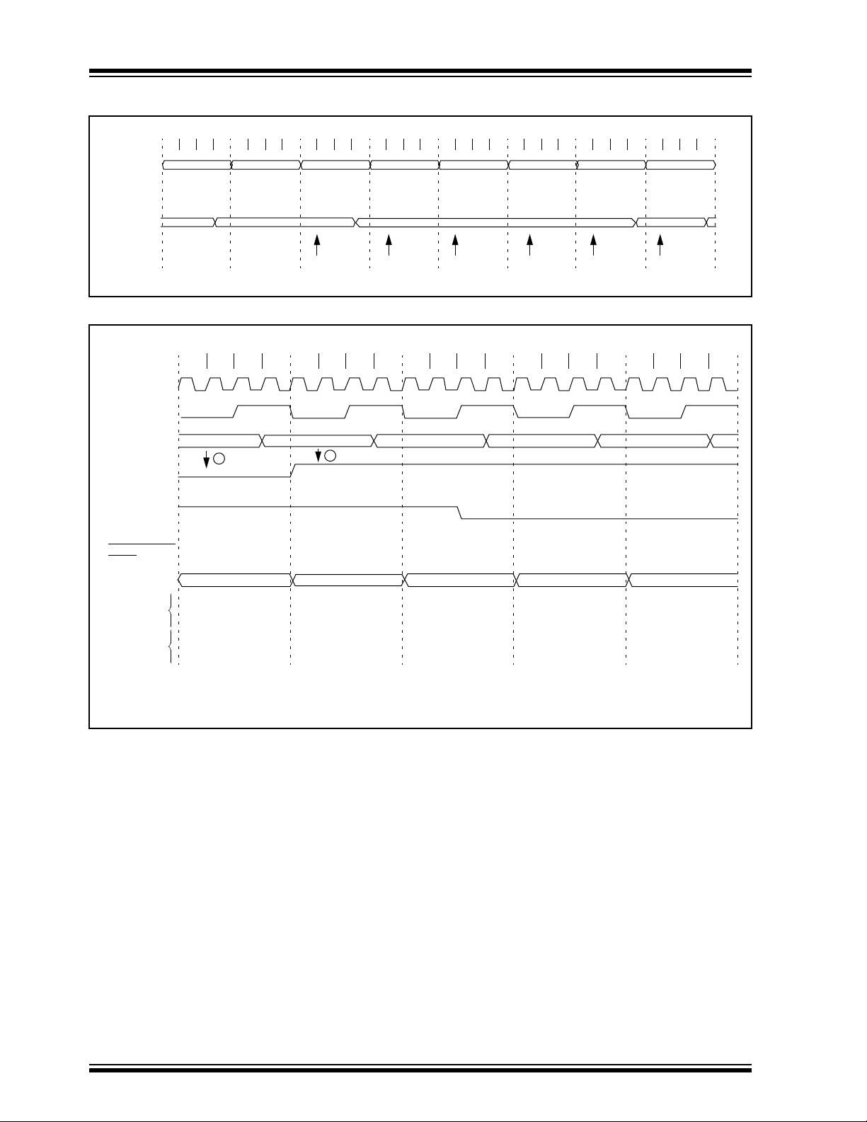
PIC16C9XX
6
FIGURE 7-3: TIMER0 TIMING: INTERNAL CLOCK/PRESCALE 1:2
PC
(Program
Counter)
Instruction
Fetch
TMR0
Instruction
Execute
Q1 Q2 Q3 Q4
PC-1
T0 NT0+1
Q1 Q2 Q3 Q4 Q1 Q2 Q3 Q4 Q1 Q2 Q3 Q4 Q1 Q2 Q3 Q4 Q1 Q2 Q3 Q4 Q1 Q2 Q3 Q4 Q1 Q2 Q3 Q4
PC PC+1 PC+2 PC+3 PC+4 PC+5 PC+6
MOVWF TMR0
MOVF TMR0,W MOVF TMR0,W MOVF TMR0,W MOVF TMR0,W MOVF TMR0,W
T0+1
Write TMR0
executed
FIGURE 7-4: TIMER0 INTERRUPT TIMING
Q2Q1 Q3 Q4Q2Q1 Q3 Q4 Q2Q1 Q3 Q4 Q2Q1 Q3 Q4 Q2Q1 Q3 Q4
OSC1
CLKOUT(3)
Timer0
T0IF bit
(INTCON<2>)
GIE bit
(INTCON<7>)
UCTION
INSTR
FLO
W
FEh
1
FFh 00h 01h 02h
1
Read TMR0
reads NT0
NT0
Read TMR0
reads NT0
Read TMR0
reads NT0
Read TMR0
reads NT0
Read TMR0
reads NT0 + 1
PC+
Instruction
fetched
Instruction
executed
PC
Note 1: Interrupt flag bit T0IF is sampled here (every Q1).
PC
Inst (PC)
Inst (PC-1)
2: Interrupt latency = 4T
3: CLKOUT is available only in RC oscillator mode.
PC +1 PC +1 0004h 0005h
Inst (PC+1)
Inst (PC)
CY where TCY = instruction cycle time.
Inst (0004h) Inst (0005h)
Inst (0004h)Dummy cycle Dummy cycle
DS30444E - page 46 1997 Microchip Technology Inc.
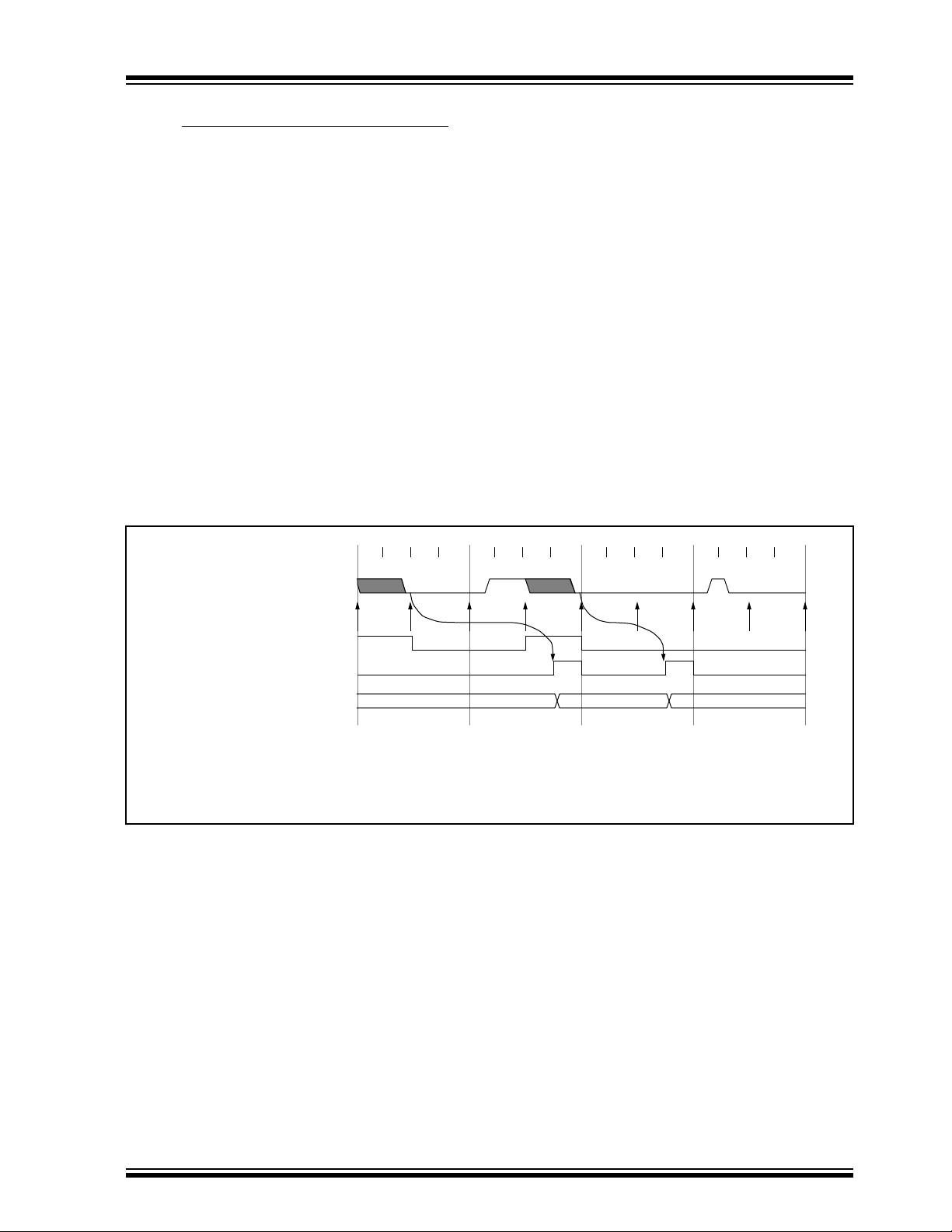
PIC16C9XX
7.2 Using Timer0 with an External Clock
When an external clock input is used for Timer0, it must
meet certain requirements. The requirements ensure
the external clock can be synchronized with the internal
phase clock (T
incrementing of Timer0 after synchronization.
7.2.1 EXTERNAL CLOCK SYNCHRONIZATION
OSC). Also, there is a delay in the actual
caler so that the prescaler output is symmetrical. For
the external clock to meet the sampling requirement,
the ripple-counter must be taken into account. Therefore, it is necessary for T0CKI to have a period of at
least 4Tosc (and a small RC delay of 40 ns) divided by
the prescaler value. The only requirement on T0CKI
high and low time is that they do not violate the minimum pulse width requirement of 10 ns. Refer to par ameters 40, 41 and 42 in the electrical specification of the
When no prescaler is used, the external clock input is
desired device.
the same as the prescaler output. The synchronization
of T0CKI with the internal phase clocks is accomplished by sampling the prescaler output on the Q2 and
Q4 cycles of the internal phase clocks (Figure 7-5).
Therefore, it is necessary for T0CKI to be high for at
least 2Tosc (and a small RC delay of 20 ns) and low for
at least 2Tosc (and a small RC delay of 20 ns). Refer to
7.2.2 TMR0 INCREMENT DELAY
Since the prescaler output is synchronized with the
internal clocks, there is a small delay from the time the
external clock edge occurs to the time the Timer0 mod-
ule is actually incremented. Figure 7-5 shows the delay
from the external clock edge to the timer incrementing.
the electrical specification of the desired device.
When a prescaler is used, the external clock input is
divided by the asynchronous ripple-counter type pres-
FIGURE 7-5: TIMER0 TIMING WITH EXTERNAL CLOCK
Q1 Q2 Q3 Q4 Q1 Q2 Q3 Q4 Q1 Q2 Q3 Q4 Q1 Q2 Q3 Q4
External Clock Input or
Prescaler output
External Clock/Prescaler
Output after sampling
Increment Timer0 (Q4)
(2)
(1)
(3)
Small pulse
misses sampling
Timer0
Note 1: Delay from clock input change to Timer0 increment is 3Tosc to 7Tosc. (Duration of Q = Tosc).
Therefore, the error in measuring the interval between two edges on Timer0 input = ±4Tosc max.
2: External clock if no prescaler selected, Prescaler output otherwise.
3: The arrows indicate the points in time where sampling occurs.
T0 T0 + 1 T0 + 2
1997 Microchip Technology Inc. DS30444E - page 47

PIC16C9XX
7.3 Prescaler
An 8-bit counter is available as a prescaler for the
Timer0 module, or as a postscaler for the Watchdog
Timer (Figure 7-6). For simplicity, this counter is being
referred to as “prescaler” throughout this data sheet.
Note that the prescaler may be used by either the
Timer0 module or the WDT but not both. Thus, a prescaler assignment for the Timer0 module means that
there is no prescaler for the Watchdog Timer, and
vice-versa.
When assigned to the Timer0 module, all instructions
writing to the TMR0 register (e.g. CLRF 1, MOVWF 1,
BSF 1,x....etc.) will clear the prescaler count. When
assigned to WDT, a CLRWDT instruction will clear the
prescaler count along with the Watchdog Timer. The
prescaler is not readable or writable.
Note: Writing to TMR0 when the prescaler is
assigned to Timer0 will clear the prescaler
count, but will not change the prescaler
assignment.
The PSA and PS2:PS0 bits (OPTION<3:0>) determine
the prescaler assignment and prescale ratio.
FIGURE 7-6: BLOCK DIAGRAM OF THE TIMER0/WDT PRESCALER
CLKOUT (=Fosc/4)
RA4/T0CKI
pin
T0SE
0
1
T0CS
M
U
X
1
M
U
0
X
PSA
SYNC
2
Cycles
Data Bus
8
TMR0 reg
Set flag bit T0IF
on Overflow
0
M
U
1
Watchdog
Timer
WDT Enable bit
Note: T0CS, T0SE, PSA, PS2:PS0 are (OPTION<5:0>).
X
PSA
8-bit Prescaler
8 - to - 1MUX
0
8
M U X
WDT
Time-out
PS2:PS0
1
PSA
DS30444E - page 48 1997 Microchip Technology Inc.

PIC16C9XX
7.3.1 SWITCHING PRESCALER ASSIGNMENT
Note: To avoid an unintended device RESET, the
The prescaler assignment is fully under software control, i.e., it can be changed “on the fly” during program
execution.
EXAMPLE 7-1: CHANGING PRESCALER (TIMER0→WDT)
Lines 2 and 3 do NOT have to
be included if the final desired
prescale value is other than 1:1.
If 1:1 is final desired value, then
a temporary prescale value is
set in lines 2 and 3 and the final
prescale value will be set in lines
10 and 11.
To change prescaler from the WDT to the Timer0 module use the precaution shown in Example 7-2.
1) BSF STATUS, RP0 ;Select Bank1
2) MOVLW b'xx0x0xxx' ;Select clock source and prescale value of
3) MOVWF OPTION_REG ;other than 1:1
4) BCF STATUS, RP0 ;Select Bank0
5) CLRF TMR0 ;Clear TMR0 and prescaler
6) BSF STATUS, RP1 ;Select Bank1
7) MOVLW b'xxxx1xxx' ;Select WDT, do not change prescale value
8) MOVWF OPTION_REG ;
9) CLRWDT ;Clears WDT and prescaler
10) MOVLW b'xxxx1xxx' ;Select new prescale value and WDT
11) MOVWF OPTION_REG ;
12) BCF STATUS, RP0 ;Select Bank0
following instruction sequence (shown in
Example 7-1) must be executed when
changing the prescaler assignment from
Timer0 to the WDT. This precaution must
be followed even if the WDT is disabled.
EXAMPLE 7-2: CHANGING PRESCALER (WDT→TIMER0)
CLRWDT ;Clear WDT and prescaler
BSF STATUS, RP0 ;Select Bank1
MOVLW b'xxxx0xxx' ;Select TMR0, new prescale value and
MOVWF OPTION_REG ;clock source
BCF STATUS, RP0 ;Select Bank0
TABLE 7-1: REGISTERS ASSOCIATED WITH TIMER0
Value on
Address Name Bit 7 Bit 6 Bit 5 Bit 4 Bit 3 Bit 2 Bit 1 Bit 0
01h, 101h TMR0 Timer0 module’s register xxxx xxxx uuuu uuuu
0Bh, 8Bh,
10Bh, 18Bh
81h, 181h OPTION RBPU INTEDG T0CS T0SE PSA PS2 PS1 PS0 1111 1111 1111 1111
85h TRISA — — PORTA Data Direction Control Register --11 1111 --11 1111
Legend: x = unknown, u = unchanged, - = unimplemented locations read as '0'. Shaded cells are not used by Timer0.
INTCON GIE PEIE T0IE INTE RBIE T0IF INTF RBIF 0000 000x 0000 000u
Power-on
Reset
Value on all
other resets
1997 Microchip Technology Inc. DS30444E - page 49

PIC16C9XX
NOTES:
DS30444E - page 50 1997 Microchip Technology Inc.

PIC16C9XX
8.0 TIMER1 MODULE
Timer1 is a 16-bit timer/counter consisting of two 8-bit
registers (TMR1H and TMR1L) which are readable and
writable. The TMR1 Register pair (TMR1H:TMR1L)
increments from 0000h to FFFFh and rolls over to
0000h. The TMR1 Interrupt, if enabled, is generated on
overflow which is latched in interrupt flag bit TMR1IF
(PIR1<0>). This interr upt can be enabled/disabled by
setting/clearing TMR1 interrupt enable bit TMR1IE
(PIE1<0>).
Timer1 can operate in one of two modes:
• As a timer
• As a counter
The operating mode is determined by the clock select
bit, TMR1CS (T1CON<1>).
In timer mode, Timer1 increments every instruction
cycle. In counter mode, it increments on every rising
edge of the external clock input.
Timer1 can be turned on and off using the control bit
TMR1ON (T1CON<0>).
Timer1 also has an internal “reset input”. This reset can
be generated by the CCP module (Section 10.0).
Figure 8-1 shows the Timer1 control register.
When the Timer1 oscillator is enabled (T1OSCEN is
set), the RC1/T1OSI and RC0/T1OSO/T1CKI pins
become inputs.
FIGURE 8-1: T1CON: TIMER1 CONTROL REGISTER (ADDRESS 10h)
U-0 U-0 R/W-0 R/W-0 R/W-0 R/W-0 R/W-0 R/W-0
— — T1CKPS1 T1CKPS0 T1OSCEN T1SYNC TMR1CS TMR1ON R = Readable bit
bit7 bit0
bit 7-6: Unimplemented: Read as '0'
bit 5-4: T1CKPS1:T1CKPS0: Timer1 Input Clock Prescale Select bits
11 = 1:8 Prescale value
10 = 1:4 Prescale value
01 = 1:2 Prescale value
00 = 1:1 Prescale value
bit 3: T1OSCEN: Timer1 Oscillator Enable Control bit
1 = Oscillator is enabled
0 = Oscillator is shut off
Note: The oscillator inverter and feedback resistor are turned off to eliminate power drain
bit 2: T1SYNC
: Timer1 External Clock Input Synchronization Control bit
W = Writable bit
U = Unimplemented bit,
- n = Value at POR reset
read as ‘0’
TMR1CS = 1
1 = Do not synchronize external clock input
0 = Synchronize external clock input
TMR1CS = 0
This bit is ignored. Timer1 uses the internal clock when TMR1CS = 0.
bit 1: TMR1CS: Timer1 Clock Source Select bit
1 = External clock from pin T1CKI (on the rising edge)
0 = Internal clock (Fosc/4)
bit 0: TMR1ON: Timer1 On bit
1 = Enables Timer1
0 = Stops Timer1
1997 Microchip Technology Inc. DS30444E - page 51

PIC16C9XX
8.1 Timer1 Operation in Timer Mode
Timer mode is selected by clearing the TMR1CS
(T1CON<1>) bit. In this mode, the input clock to the
timer is Fosc/4. The synchronize control bit T1SYNC
(T1CON<2>) has no effect since the internal clock is
always in sync.
8.2 Timer1 Operation in Synchronized
Counter Mode
Counter mode is selected by setting bit TMR1CS. In
this mode the timer increments on every rising edge of
clock input on pin RC1/T1OSI when bit T1OSCEN is
set or pin RC0/T1OSO/T1CKI when bit T1OSCEN is
cleared.
If T1SYNC
synchronized with internal phase clocks. The synchronization is done after the prescaler stage. The prescaler is an asynchronous ripple-counter.
In this configuration, during SLEEP mode, Timer1 will
not increment even if the external clock is present,
since the synchronization circuit is shut off. The prescaler however will continue to increment.
is cleared, then the external clock input is
8.2.1 EXTERNAL CLOCK INPUT TIMING FOR
SYNCHRONIZED COUNTER MODE
When an external clock input is used for Timer1 in synchronized counter mode, it must meet certain requirements. The external clock requirement is due to
internal phase clock (T osc) synchronization. Also, there
is a delay in the actual incrementing of TMR1 after synchronization.
When the prescaler is 1:1, the external clock input is
the same as the prescaler output. The synchronization
of T1CKI with the internal phase clocks is accomplished by sampling the prescaler output on the Q2 and
Q4 cycles of the internal phase clocks. Therefore, it is
necessary for T1CKI to be high for at least 2Tosc (and
a small RC delay of 20 ns) and low for at least 2Tosc
(and a small RC delay of 20 ns). Refer to the appropriate electrical specifications, parameters 45, 46, and 47.
When a prescaler other than 1:1 is used, the external
clock input is divided by the asynchronous ripple-counter type prescaler so that the prescaler output
is symmetrical. In order for the external clock to meet
the sampling requirement, the ripple-counter must be
taken into account. Therefore, it is necessary f or T1CKI
to have a period of at least 4Tosc (and a small RC delay
of 40 ns) divided by the prescaler value. The only
requirement on T1CKI high and low time is that the y do
not violate the minimum pulse width requirements of
10 ns). Refer to the appropriate electrical specifications, parameters 40, 42, 45, 46, and 47.
FIGURE 8-2: TIMER1 BLOCK DIAGRAM
Set flag bit
TMR1IF on
Overflow
RC0/T1OSO/T1CKI
RC1/T1OSI
Note 1: When the T1OSCEN bit is cleared, the inverter and feedback resistor are turned off. This eliminates power drain.
TMR1H
T1OSC
TMR1
TMR1L
T1OSCEN
Enable
Oscillator
(1)
Fosc/4
Internal
Clock
TMR1ON
on/off
1
0
T1CKPS1:T1CKPS0
TMR1CS
0
1
T1SYNC
Prescaler
1, 2, 4, 8
2
Synchronized
clock input
Synchronize
det
SLEEP input
DS30444E - page 52 1997 Microchip Technology Inc.
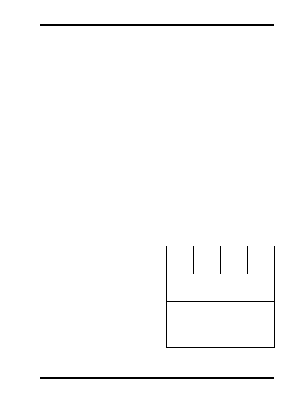
PIC16C9XX
8.3 Timer1 Operation in Asynchronous
Counter Mode
If control bit T1SYNC (T1CON<2>) is set, the external
clock input is not synchronized. The timer continues to
increment asynchronous to the internal phase clocks.
The timer will continue to run during SLEEP and can
generate an interrupt on overflow which will wake-up
the processor. However, special precautions in software are needed to read-from or write-to the Timer1
register pair (TMR1H:TMR1L) (Section 8.3.2).
In asynchronous counter mode, Timer1 cannot be used
as a time-base for capture or compare operations.
8.3.1 EXTERNAL CLOCK INPUT TIMING WITH
UNSYNCHRONIZED CLOCK
If control bit T1SYNC
completely asynchronously. The input clock must meet
certain minimum high time and low time requirements,
as specified in timing parameters 45, 46, and 47.
8.3.2 READING AND WRITING TMR1 IN
ASYNCHRONOUS COUNTER MODE
Reading TMR1H or TMR1L while the timer is running,
from an external asynchronous clock, will ensure a
valid read (taken care of in hardware). However, the
user should keep in mind that reading the 16-bit timer
in two 8-bit values itself poses certain problems since
the timer may overflow between the reads.
For writes, it is recommended that the user simply stop
the timer and write the desired values. A write contention may occur by writing to the timer registers while the
register is incrementing. This may produce an unpredictable value in the timer register.
Reading the 16-bit value requires some care.
Example 8-1 is an example routine to read the 16-bit
timer value. This is useful if the timer cannot be
stopped.
is set, the timer will increment
EXAMPLE 8-1: READING A 16-BIT
FREE-RUNNING TIMER
; All interrupts are disabled
MOVF TMR1H, W ;Read high byte
MOVWF TMPH ;
MOVF TMR1L, W ;Read low byte
MOVWF TMPL ;
MOVF TMR1H, W ;Read high byte
SUBWF TMPH, W ;Sub 1st read
; with 2nd read
BTFSC STATUS,Z ;Is result = 0
GOTO CONTINUE ;Good 16-bit read
;
; TMR1L may have rolled over between the read
; of the high and low bytes. Reading the high
; and low bytes now will read a good value.
;
MOVF TMR1H, W ;Read high byte
MOVWF TMPH ;
MOVF TMR1L, W ;Read low byte
MOVWF TMPL ;
; Re-enable the Interrupt (if required)
CONTINUE ;Continue with your code
8.4 Timer1 Oscillator
A crystal oscillator circuit is built in between pins T1OSI
(input) and T1OSO (amplifier output). It is enabled by
setting control bit T1OSCEN (T1CON<3>). The oscillator is a low power oscillator rated up to 200 kHz. It will
continue to run during SLEEP. It is primarily intended
for a 32 kHz crystal. Table 8-1 shows the capacitor
selection for the Timer1 oscillator.
The Timer1 oscillator is identical to the LP oscillator.
The user must provide a software time delay to ensure
proper oscillator start-up.
TABLE 8-1: CAPACITOR SELECTION FOR
THE TIMER1 OSCILLATOR
Osc Type Freq C1 C2
LP 32 kHz 33 pF 33 pF
100 kHz 15 pF 15 pF
200 kHz 15 pF 15 pF
These values are for design guidance only.
Crystals Tested:
32.768 kHz Epson C-001R32.768K-A ± 20 PPM
100 kHz Epson C-2 100.00 KC-P ± 20 PPM
200 kHz STD XTL 200.000 kHz ± 20 PPM
Note 1: Higher capacitance increases the stability
of oscillator but also increases the start-up
time.
2: Since each resonator/crystal has its own
characteristics, the user should consult the
resonator/crystal manufacturer for appropriate values of external components.
1997 Microchip Technology Inc. DS30444E - page 53

PIC16C9XX
8.5 Resetting Timer1 using the CCP
Trigger Output
If the CCP1 module is configured in compare mode to
generate a “special event trigger" (CCP1M3:CCP1M0
= 1011), this signal will reset Timer1.
Note: The special event trigger from the CCP1
module will not set interrupt flag bit
TMR1IF (PIR1<0>).
Timer1 must be configured for either timer or synchronized counter mode to take advantage of this f eature. If
Timer1 is running in asynchronous counter mode, this
8.6 Resetting of Timer1 Register Pair
(TMR1H:TMR1L)
TMR1H and TMR1L registers are not reset on a POR
or any other reset except by the CCP1 special event
trigger.
T1CON register is reset to 00h on a Pow er-on Reset. In
any other reset, the register is unaffected.
8.7 Timer1 Prescaler
The prescaler counter is cleared on writes to the
TMR1H or TMR1L registers.
reset operation may not work.
In the event that a write to Timer1 coincides with a spe-
cial event trigger from CCP1, the write will take precedence.
In this mode of operation, the CCPR1H:CCPR1L registers pair effectively becomes the period register for
Timer1.
TABLE 8-2: REGISTERS ASSOCIATED WITH TIMER1 AS A TIMER/COUNTER
Address Name Bit 7 Bit 6 Bit 5 Bit 4 Bit 3 Bit 2 Bit 1 Bit 0
0Bh, 8Bh,
10Bh, 18Bh
0Ch PIR1 LCDIF ADIF
8Ch PIE1
0Eh TMR1L Holding register for the Least Significant Byte of the 16-bit TMR1 register
0Fh TMR1H Holding register for the Most Significant Byte of the 16-bit TMR1 register
10h T1CON
Legend: x = unknown, u = unchanged, - = unimplemented read as '0'. Shaded cells are not used by theTimer1 module.
Note 1: Bits ADIE and ADIF are reserved on the PIC16C923, always maintain these bits clear.
INTCON GIE PEIE
LCDIE ADIE
— — T1CKPS1 T1CKPS0 T1OSCEN T1SYNC TMR1CS TMR1ON
T0IE INTE RBIE T0IF INTF RBIF
(1)
— — SSPIF CCP1IF TMR2IF TMR1IF
(1)
— — SSPIE CCP1IE TMR2IE TMR1IE
Value on
Power-on
Reset
0000 000x 0000 000u
00-- 0000 00-- 0000
00-- 0000 00-- 0000
xxxx xxxx uuuu uuuu
xxxx xxxx uuuu uuuu
--00 0000 --uu uuuu
Value on
all other
resets
DS30444E - page 54 1997 Microchip Technology Inc.

PIC16C9XX
9.0 TIMER2 MODULE
Timer2 is an 8-bit timer with a prescaler and a
postscaler. It can be used as the PWM time-base for
the PWM mode of the CCP module. The TMR2 register
is readable and writable, and is cleared on any device
reset.
The input clock (F
1:4 or 1:16 (selected by control bits
T2CKPS1:T2CKPS0 (T2CON<1:0>)).
The Timer2 module has an 8-bit period register, PR2.
TMR2 increments from 00h until it matches PR2 and
then resets to 00h on the next increment cycle. PR2 is
a readable and writable register . The PR2 register is set
during RESET.
The match output of TMR2 goes through a 4-bit
postscaler (which gives a 1:1 to 1:16 scaling inclusive)
to generate a TMR2 interrupt (latched in flag bit
TMR2IF, (PIR1<1>)).
Timer2 can be shut off by clearing control bit TMR2ON
(T2CON<2>) to minimize power consumption.
Figure 9-2 shows the Timer2 control register.
OSC/4) has a prescale option of 1:1,
9.1 Timer2 Prescaler and Postscaler
The prescaler and postscaler counters are cleared
when any of the following occurs:
• a write to the TMR2 register
• a write to the T2CON register
• any device reset (Power-on Reset, MCLR
Reset,
or Watchdog Timer Reset)
TMR2 will not clear when T2CON is written.
9.2 Output of TMR2
The output of TMR2 (bef ore the postscaler) is fed to the
Synchronous Serial Port module which optionally uses
it to generate shift clock.
FIGURE 9-1: TIMER2 BLOCK DIAGRAM
(1)
Postscaler
1:16
4
Sets flag
bit TMR2IF
1:1
to
Fosc/4
Prescaler
1:1, 1:4, 1:16
2
TMR2 reg
Comparator
PR2 reg
TMR2
output
Reset
EQ
Note 1: TMR2 register output can be software selected
by the SSP Module as the source clock.
FIGURE 9-2: T2CON: TIMER2 CONTROL REGISTER (ADDRESS 12h)
U-0 R/W-0 R/W-0 R/W-0 R/W-0 R/W-0 R/W-0 R/W-0
— TOUTPS3 TOUTPS2 TOUTPS1 TOUTPS0 TMR2ON T2CKPS1 T2CKPS0 R = Readable bit
bit7 bit0
bit 7: Unimplemented: Read as '0'
bit 6-3: TOUTPS3:TOUTPS0: Timer2 Output Postscale Select bits
0000 = 1:1 Postscale
0001 = 1:2 Postscale
•
•
•
1111 = 1:16 Postscale
bit 2: TMR2ON: Timer2 On bit
1 = Timer2 is on
0 = Timer2 is off
bit 1-0: T2CKPS1:T2CKPS0: Timer2 Clock Prescale Select bits
00 = Prescaler is 1
01 = Prescaler is 4
1x = Prescaler is 16
W = Writable bit
U = Unimplemented bit,
- n = Value at POR reset
read as ‘0’
1997 Microchip Technology Inc. DS30444E - page 55

PIC16C9XX
TABLE 9-1: REGISTERS ASSOCIATED WITH TIMER2 AS A TIMER/COUNTER
Address Name Bit 7 Bit 6 Bit 5 Bit 4 Bit 3 Bit 2 Bit 1 Bit 0
0Bh, 8Bh,
10Bh, 18Bh
0Ch PIR1 LCDIF ADIF
8Ch PIE1
11h TMR2 Timer2 module’s register
12h T2CON
92h PR2 Timer2 Period Register
Legend: x = unknown, u = unchanged, - = unimplemented read as '0'. Shaded cells are not used by the Timer2 module.
Note 1: Bits ADIE and ADIF are reserved on the PIC16C923, always maintain these bits clear.
INTCON GIE PEIE
LCDIE ADIE
— TOUTPS3 TOUTPS2 TOUTPS1 TOUTPS0 TMR2ON T2CKPS1 T2CKPS0
T0IE INTE RBIE T0IF INTF RBIF
(1)
(1)
— — SSPIF CCP1IF TMR2IF TMR1IF
— — SSPIE CCP1IE TMR2IE TMR1IE
Value on
Power-on
Reset
0000 000x 0000 000u
00-- 0000 00-- 0000
00-- 0000 00-- 0000
0000 0000 0000 0000
-000 0000 -000 0000
1111 1111 1111 1111
Value on
all other
resets
DS30444E - page 56 1997 Microchip Technology Inc.

PIC16C9XX
10.0 CAPTURE/COMPARE/PWM (CCP) MODULE
The CCP (Capture/Compare/PWM) module contains a
16-bit register which can operate as a 16-bit capture
register, as a 16-bit compare register, or as a PWM
master/slave duty cycle register. Table 10-1 shows the
timer resources used by the CCP module.
Capture/Compare/PWM Register1 (CCPR1) is comprised of two 8-bit registers: CCPR1L (low byte) and
CCPR1H (high byte). The CCP1CON register controls
the operation of CCP1. All three are readable and writable.
Figure 10-1 shows the CCP1CON register.
For use of the CCP module, refer to the
Control Handbook,
"Using the CCP Modules" (AN594).
T ABLE 10-1: CCP MODE - TIMER RESOURCE
CCP Mode Timer Resource
Capture
Compare
PWM
FIGURE 10-1: CCP1CON REGISTER (ADDRESS 17h)
U-0 U-0 R/W-0 R/W-0 R/W-0 R/W-0 R/W-0 R/W-0
— — CCP1X CCP1Y CCP1M3 CCP1M2 CCP1M1 CCP1M0 R = Readable bit
bit7 bit0
bit 7-6: Unimplemented: Read as '0'
bit 5-4: CCP1X:CCP1Y: PWM Least Significant bits
Capture Mode
Unused
Compare Mode
Unused
PWM Mode
These bits are the two LSbs of the PWM duty cycle. The eight MSbs are found in CCPR1L.
bit 3-0: CCP1M3:CCP1M0: CCP1 Mode Select bits
0000 = Capture/Compare/PWM off (resets CCP1 module)
0100 = Capture mode, every falling edge
0101 = Capture mode, every rising edge
0110 = Capture mode, every 4th rising edge
0111 = Capture mode, every 16th rising edge
1000 = Compare mode, set output on match (bit CCP1IF is set)
1001 = Compare mode, clear output on match (bit CCP1IF is set)
1010 = Compare mode, generate software interrupt on match (bit CCP1IF is set, CCP1 pin is unaffected)
1011 = Compare mode, trigger special event (CCP1IF bit is set; CCP1 resets TMR1)
11xx = PWM mode
W =Writable bit
U = Unimplemented bit,
read as ‘0’
- n =Value at POR reset
Embedded
Timer1
Timer1
Timer2
1997 Microchip Technology Inc. DS30444E - page 57

PIC16C9XX
10.1 Capture Mode
In Capture mode, CCPR1H:CCPR1L captures the
16-bit value of the TMR1 register when an e v ent occurs
on pin RC2/CCP1 (Figure 10-2). An event is defined as:
• Every falling edge
• Every rising edge
• Every 4th rising edge
• Every 16th rising edge
An event is selected by control bits CCP1M3:CCP1M0
(CCP1CON<3:0>). When a capture is made, the interrupt request flag bit CCP1IF (PIR1<2>) is set. It must
be cleared in software. If another capture occurs before
the value in register CCPR1 is read, the old captured
value will be lost.
10.1.1 CCP PIN CONFIGURATION
In capture mode, the RC2/CCP1 pin should be config-
ured as an input by setting the TRISC<2> bit.
Note: If the RC2/CCP1 pin is configured as an
output, a write to the port can cause a capture condition.
FIGURE 10-2: CAPTURE MODE OPERATION
BLOCK DIAGRAM
CCP
Prescaler
÷ 1, 4, 16
RC2/CCP1
pin
and
edge detect
CCP1CON<3:0>
Q’s
10.1.2 TIMER1 MODE SELECTION
Timer1 must be running in timer mode or synchronized
counter mode for the CCP module to use the capture
feature. In asynchronous counter mode the capture
operation may not work.
Set CCP1IF
PIR1<2>
Capture
Enable
CCPR1H CCPR1L
TMR1H TMR1L
Switching from one capture prescaler to another may
generate an interrupt. Also, the prescaler counter will
not be cleared, therefore the first capture may be from
a non-zero prescaler. Example 10-1 shows the recommended method for switching between capture prescalers. This example also clears the prescaler counter and
will not generate the “false” interrupt.
EXAMPLE 10-1: CHANGING BETWEEN
CAPTURE PRESCALERS
CLRF CCP1CON ; Turn CCP module off
MOVLW NEW_CAPT_PS ; Load the W reg with
; the new prescaler
; mode value and CCP ON
MOVWF CCP1CON ; Load CCP1CON with
; this value
10.2 Compare Mode
In Compare mode, the 16-bit CCPR1 register value is
constantly compared against the TMR1 register pair
value. When a match occurs, the RC2/CCP1 pin is:
• Driven High
• Driven Low
• Remains Unchanged
The action on the pin is based on the value of control
bits CCP1M3:CCP1M0 (CCP1CON<3:0>). At the
same time, a compare interrupt is also generated.
FIGURE 10-3: COMPARE MODE
OPERATION BLOCK DIAGRAM
Special event trigger will reset Timer1, but not
set interrupt flag bit TMR1IF (PIR1<0>).
Set CCP1IF
PIR1<2>
CCPR1H CCPR1L
match
Comparator
TMR1H TMR1L
RC2/CCP1
TRISC<2>
Output Enable
Trigger
Q S
Output
Logic
R
CCP1CON<3:0>
Mode Select
10.1.3 SOFTWARE INTERRUPT
When the Capture mode is changed, a false capture
interrupt may be generated. The user should keep
enable bit CCP1IE (PIE1<2>) clear to avoid false interrupts and should clear flag bit CCP1IF following any
such change in operating mode.
10.1.4 CCP PRESCALER
There are four prescaler settings, specified by bits
10.2.1 CCP PIN CONFIGURATION
The user must configure the RC2/CCP1 pin as an out-
put by clearing the TRISC<2> bit.
Note: Clearing the CCP1CON register will force
the RC2/CCP1 compare output latch to the
default low level. This is not the data latch.
CCP1M3:CCP1M0. Whenever the CCP module is
turned off, or the CCP module is not in Capture mode,
the prescaler counter is cleared. This means that any
reset will clear the prescaler counter.
DS30444E - page 58 1997 Microchip Technology Inc.

PIC16C9XX
10.2.1 TIMER1 MODE SELECTION
Timer1 must be running in Timer mode or Synchronized Counter mode if the CCP module is using the
compare feature. In Asynchronous Counter mode, the
compare operation may not work.
10.2.2 SOFTWARE INTERRUPT MODE
When Generate Software Interrupt is chosen, the
CCP1 pin is not affected. Only a CCP interrupt is generated (if enabled).
10.2.3 SPECIAL EVENT TRIGGER
In this mode, an internal hardware trigger is generated
which may be used to initiate an action.
The special event trigger output of CCP1 resets the
TMR1 register pair and starts an A/D conversion. This
allows the CCPR1H:CCPR1L register pair to effectively
be a 16-bit programmable period register for Timer1.
Note: The "special event trigger" from the CCP1
module will not set interrupt flag bit
TMR1IF (PIR1<0>).
10.3 PWM Mode
In Pulse Width Modulation (PWM) mode, the CCP1 pin
produces up to a 10-bit resolution PWM output. Since
the CCP1 pin is multiplexed with the POR TC data latch,
the TRISC<2> bit must be cleared to make the CCP1
pin an output.
Note: Clearing the CCP1CON register will force
the CCP1 PWM output latch to the default
low level. This is not the PORTC I/O data
latch.
Figure 10-4 shows a simplified block diagram of the
CCP module in PWM mode.
For a step by step procedure on how to set up the CCP
module for PWM operation, see Section 10.3.3.
FIGURE 10-4: SIMPLIFIED PWM BLOCK
DIAGRAM
Duty cycle registers
CCPR1L
CCPR1H (Slave)
Comparator
TMR2
Comparator
PR2
Note 1: 8-bit timer is concatenated with 2-bit internal Q clock
or 2 bits of the prescaler to create 10-bit time-base.
(Note 1)
Clear Timer,
CCP1 pin and
latch D.C.
A PWM output (Figure 10-5) has a time-base (period)
and a time that the output stays high (duty cycle). The
frequency of the PWM is the inverse of the period
(1/period).
CCP1CON<5:4>
R
S
Q
RC1/CCP1
TRISC<2>
FIGURE 10-5: PWM OUTPUT
Period
Duty Cycle
TMR2 = PR2
TMR2 = PR2
TMR2 = Duty Cycle
10.3.1 PWM PERIOD
The PWM period is specified by writing to the PR2 reg-
ister. The PWM period can be calculated using the following formula:
PWM period = [ (PR2) + 1 ] • 4 • T
OSC •
(TMR2 prescale value)
PWM frequency is defined as 1 / [PWM period].
When TMR2 is equal to PR2, the following three events
occur on the next increment cycle:
• TMR2 is cleared
• The CCP1 pin is set (exception: if PWM duty
cycle = 0%, the CCP1 pin will not be set)
• The PWM duty cycle is latched from CCPR1L into
CCPR1H
1997 Microchip Technology Inc. DS30444E - page 59

PIC16C9XX
Note: The Timer2 postscaler (Section 9.0) is not
used in the determination of the PWM frequency. The postscaler could be used to
have a servo update rate at a different frequency than the PWM output.
10.3.2 PWM DUTY CYCLE
The PWM duty cycle is specified by writing to the
CCPR1L register and to the CCP1CON<5:4> bits. Up
to 10-bit resolution is available: the CCPR1L contains
the eight MSbs and CCP1CON<5:4> contains the two
LSbs. This 10-bit value is represented by
CCPR1L:CCP1CON<5:4>. The following equation is
used to calculate the PWM duty cycle in time:
PWM duty cycle = (CCPR1L:CCP1CON<5:4>) •
Tosc • (TMR2 prescale value)
CCPR1L and CCP1CON<5:4> can be written to at any
time, but the duty cycle value is not latched into
CCPR1H until after a match between PR2 and TMR2
occurs (i.e., the period is complete). In PWM mode,
CCPR1H is a read-only register.
The CCPR1H register and a 2-bit internal latch are
used to double buffer the PWM duty cycle. This double
buffering is essential for glitchless PWM operation.
When the CCPR1H and 2-bit latch match TMR2 concatenated with an internal 2-bit Q clock or 2 bits of the
TMR2 prescaler, the CCP1 pin is cleared.
Maximum PWM resolution (bits) for a given PWM frequency:
OSC
F
F
PWM
)
bits
log(
=
log(2)
Note: If the PWM duty cycle value is longer than
the PWM period the CCP1 pin will not be
cleared.
EXAMPLE 10-2: PWM PERIOD AND DUTY
CYCLE CALCULATION
Desired PWM frequency is 31.25 kHz,
Fosc = 8 MHz
TMR2 prescale = 1
1/31.25 kHz = [ (PR2) + 1 ] • 4 • 1/8 MHz • 1
32 µs = [ (PR2) + 1 ] • 4 • 125 ns • 1
PR2 = 63
Find the maximum resolution of the duty cycle that can
be used with a 31.25 kHz frequency and 8 MHz oscillator:
1/31.25 kHz = 2
32 µs = 2
256 = 2
log(256) = (PWM Resolution) • log(2)
8.0 = PWM Resolution
At most, an 8-bit resolution duty cycle can be obtained
from a 31.25 kHz frequency and a 8 MHz oscillator, i.e.,
0 ≤ CCPR1L:CCP1CON<5:4> ≤ 255. An y value greater
than 255 will result in a 100% duty cycle.
In order to achieve higher resolution, the PWM frequency must be decreased. In order to achieve higher
PWM frequency, the resolution must be decreased.
Table 10-2 lists example PWM frequencies and resolutions for Fosc = 8 MHz. TMR2 prescaler and PR2 values are also shown.
10.3.3 SET-UP FOR PWM OPERATION
The following steps should be taken when configuring
the CCP module for PWM operation:
1. Set the PWM period by writing to the PR2 register.
2. Set the PWM duty cycle by writing to the
CCPR1L register and CCP1CON<5:4> bits.
3. Make the CCP1 pin an output by clearing the
TRISC<2> bit.
4. Set the TMR2 prescale value and enable Timer2
by writing to T2CON.
5. Configure the CCP module for PWM operation.
PWM RESOLUTION
PWM RESOLUTION
PWM RESOLUTION
• 1/8 MHz • 1
• 125 ns • 1
TABLE 10-2: EXAMPLE PWM FREQUENCIES AND RESOLUTIONS AT 8 MHz
PWM Frequency 488 Hz 1.95 kHz 7.81 kHz 31.25 kHz 62.5 kHz 250 kHz
Timer Prescaler (1, 4, 16) 16 4 1 1 1 1
PR2 Value 0xFF 0xFF 0xFF 0x3F 0x1F 0x07
Maximum Resolution (bits) 10 10 10 8 7 5
DS30444E - page 60 1997 Microchip Technology Inc.
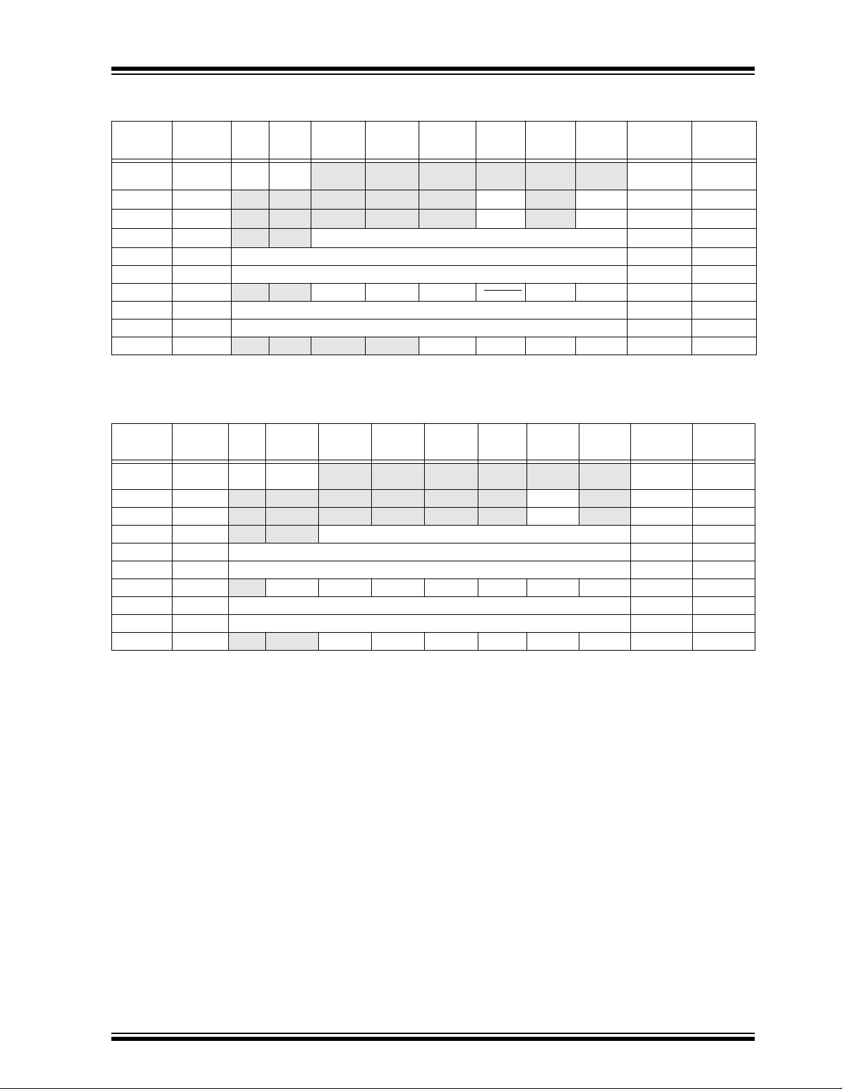
PIC16C9XX
TABLE 10-3: REGISTERS ASSOCIATED WITH TIMER1, CAPTURE AND COMPARE
Address Name Bit 7 Bit 6 Bit 5 Bit 4 Bit 3 Bit 2 Bit 1 Bit 0
0Bh, 8Bh,
10Bh, 18Bh
0Ch PIR1 LCDIF ADIF
8Ch PIE1 LCDIE ADIE
87h TRISC — — PORTC Data Direction Control Register --11 1111 --11 1111
0Eh TMR1L Holding register for the Least Significant Byte of the 16-bit TMR1 register
0Fh TMR1H Holding register for the Most Significant Byte of the 16-bit TMR1 register
10h T1CON
15h CCPR1L Capture/Compare/PWM1 (LSB)
16h CCPR1H Capture/Compare/PWM1 (MSB)
17h CCP1CON
Legend: x = unknown, u = unchanged, - = unimplemented locations read as '0’. Shaded cells are not used in these modes.
Note 1: Bits ADIE and ADIF reserved on the PIC16C923, always maintain these bits clear.
INTCON GIE PEIE T0IE INTE RBIE T0IF INTF RBIF
(1)
— — SSPIF CCP1IF TMR2IF TMR1IF
(1)
— — SSPIE CCP1IE TMR2IE TMR1IE
— — T1CKPS1 T1CKPS0 T1OSCEN T1SYNC TMR1CS TMR1ON
— — CCP1X CCP1Y CCP1M3 CCP1M2 CCP1M1 CCP1M0
Value on
Power-on
Reset
0000 000x 0000 000u
00-- 0000 00-- 0000
00-- 0000 00-- 0000
xxxx xxxx uuuu uuuu
xxxx xxxx uuuu uuuu
--00 0000 --uu uuuu
xxxx xxxx uuuu uuuu
xxxx xxxx uuuu uuuu
--00 0000 --00 0000
Value on
all other
Resets
TABLE 10-4: REGISTERS ASSOCIATED WITH PWM AND TIMER2
Address Name Bit 7 Bit 6 Bit 5 Bit 4 Bit 3 Bit 2 Bit 1 Bit 0
0Bh, 8Bh,
10Bh, 18Bh
0Ch PIR1
8Ch PIE1
87h TRISC
11h TMR2 Timer2 module’s register 0000 0000 0000 0000
92h PR2 Timer2 module’s Period register 1111 1111 1111 1111
12h T2CON
15h CCPR1L Capture/Compare/PWM1 (LSB) xxxx xxxx uuuu uuuu
16h CCPR1H Capture/Compare/PWM1 (MSB) xxxx xxxx uuuu uuuu
17h CCP1CON
Legend: x = unknown, u = unchanged, - = unimplemented locations read as '0’. Shaded cells are not used in this mode.
Note 1: Bits ADIE and ADIF reserved on the PIC16C923, always maintain these bits clear.
INTCON GIE PEIE
LCDIF ADIF
LCDIE ADIE
— — PORTC Data Direction Control Register --11 1111 --11 1111
— TOUTPS3 TOUTPS2 TOUTPS1 TOUTPS0 TMR2ON T2CKPS1 T2CKPS0 -000 0000 -000 0000
— — CCP1X CCP1Y CCP1M3 CCP1M2 CCP1M1 CCP1M0 --00 0000 --00 0000
T0IE INTE RBIE T0IF INTF RBIF 0000 000x 0000 000u
(1)
(1)
— — SSPIF CCP1IF TMR2IF TMR1IF 00-- 0000 00-- 0000
— — SSPIE CCP1IE TMR2IE TMR1IE 00-- 0000 00-- 0000
Value on
Power-on
Reset
Value on
all other
Resets
1997 Microchip Technology Inc. DS30444E - page 61

PIC16C9XX
NOTES:
DS30444E - page 62 1997 Microchip Technology Inc.

PIC16C9XX
11.0 SYNCHRONOUS SERIAL PORT (SSP) MODULE
The Synchronous Serial Port (SSP) module is a serial
interface useful for communicating with other peripheral or microcontroller devices. These peripheral
devices may be serial EEPROMs, shift registers, dis-
play drivers, A/D converters, etc. The SSP module can
operate in one of two modes:
• Serial Peripheral Interface (SPI)
• Inter-Integrated Circuit (I
Refer to Application Note AN578,
Module in the I
2
C Multi-Master Environment."
2
C)
FIGURE 11-1: SSPSTAT: SYNC SERIAL PORT STATUS REGISTER (ADDRESS 94h)
R/W-0 R/W-0 R-0 R-0 R-0 R-0 R-0 R-0
SMP CKE D/A
bit7 bit0
bit 7: SMP: SPI data input sample phase
SPI Master Mode
1 = Input data sampled at end of data output time
0 = Input data sampled at middle of data output time
SPI Sla
ve Mode
SMP must be cleared when SPI is used in slave mode
bit 6: CKE: SPI Clock Edge Select (Figure 11-5, Figure 11-6, and Figure 11-7)
CKP = 0
1 = Data transmitted on rising edge of SCK
0 = Data transmitted on falling edge of SCK
CKP = 1
1 = Data transmitted on falling edge of SCK
0 = Data transmitted on rising edge of SCK
bit 5: D/A
bit 4: P: Stop bit (I
bit 3: S: Start bit (I
bit 2: R/W
bit 1: UA: Update Address (10-bit I
bit 0: BF: Buffer Full Status bit
: Data/Address bit (I2C mode only)
1 = Indicates that the last byte received or transmitted was data
0 = Indicates that the last byte received or transmitted was address
2
C mode only. This bit is cleared when the SSP module is disabled, or when the Start bit was
detected last)
1 = Indicates that a stop bit has been detected last (this bit is '0' on RESET)
0 = Stop bit was not detected last
2
detected last)
1 = Indicates that a start bit has been detected last (this bit is '0' on RESET)
0 = Start bit was not detected last
: Read/Write bit information (I2C mode only)
This bit holds the R/W bit information following the last address match. This bit is only valid from the
address match to the next start bit, stop bit, or A
1 = Read
0 = Write
1 = Indicates that the user needs to update the address in the SSPADD register
0 = Address does not need to be updated
e (SPI and I2C modes)
Receiv
1 = Receive complete, SSPBUF is full
0 = Receive not complete, SSPBUF is empty
T
ransmit (I2C mode only)
1 = Transmit in progress, SSPBUF is full
0 = Transmit complete, SSPBUF is empty
P S R/W UA BF R = Readable bit
W =Writable bit
U = Unimplemented bit,
read as ‘0’
- n =Value at POR reset
C mode only. This bit is cleared when the SSP module is disabled, or when the Stop bit w as
CK bit.
2
C mode only)
"Use of the SSP
1997 Microchip Technology Inc. DS30444E - page 63

PIC16C9XX
FIGURE 11-2: SSPCON: SYNC SERIAL PORT CONTROL REGISTER (ADDRESS 14h)
R/W-0 R/W-0 R/W-0 R/W-0 R/W-0 R/W-0 R/W-0 R/W-0
WCOL SSPOV SSPEN CKP SSPM3 SSPM2 SSPM1 SSPM0 R = Readable bit
bit7 bit0
bit 7: WCOL: Write Collision Detect bit
1 = The SSPBUF register is written while it is still transmitting the previous word
(must be cleared in software)
0 = No collision
bit 6: SSPOV: Receive Overflow Indicator bit
In SPI mode
1 = A new byte is received while the SSPB UF register is still holding the previous data. In case of ov erflow ,
the data in SSPSR is lost. Ov erflow can only occur in sla v e mode. The user must read the SSPBUF, even
if only transmitting data, to avoid setting overflow. In master mode the overflow bit is not set since each
new reception (and transmission) is initiated by writing to the SSPBUF register.
0 = No overflow
2
In I
C mode
1 = A byte is received while the SSPBUF register is still holding the pre vious byte. SSPO V is a "don’t care"
in transmit mode. SSPOV must be cleared in software in either mode.
0 = No overflow
bit 5: SSPEN: Synchronous Serial Port Enable bit
In SPI mode
1 = Enables serial port and configures SCK, SDO, and SDI as serial port pins
0 = Disables serial port and configures these pins as I/O port pins
2
C mode
In I
1 = Enables the serial port and configures the SDA and SCL pins as serial port pins
0 = Disables serial port and configures these pins as I/O port pins
In both modes, when enabled, these pins must be properly configured as input or output.
bit 4: CKP: Clock Polarity Select bit
In SPI mode
1 = Idle state for clock is a high level
0 = Idle state for clock is a low level
2
In I
C mode
SCK release control
1 = Enable clock
0 = Holds clock low (clock stretch) (Used to ensure data setup time)
bit 3-0: SSPM3:SSPM0: Synchronous Serial Port Mode Select bits
0000 = SPI master mode, clock = F
0001 = SPI master mode, clock = F
0010 = SPI master mode, clock = F
OSC/4
OSC/16
OSC/64
0011 = SPI master mode, clock = TMR2 output/2
0100 = SPI slave mode, clock = SCK pin. SS
0101 = SPI slave mode, clock = SCK pin. SS
0110 = I
0111 = I
1011 = I
1110 = I
1111 = I
2
C slave mode, 7-bit address
2
C slave mode, 10-bit address
2
C Firmware controlled master mode (slave idle)
2
C slave mode, 7-bit address with start and stop bit interrupts enabled
2
C slave mode, 10-bit address with start and stop bit interrupts enabled
pin control enabled.
pin control disabled. SS can be used as I/O pin
W =Writable bit
U = Unimplemented bit,
read as ‘0’
- n =Value at POR reset
DS30444E - page 64 1997 Microchip Technology Inc.

PIC16C9XX
11.1 SPI Mode
The SPI mode allows 8-bits of data to be synchronously transmitted and received simultaneously. To
accomplish communication, typically three pins are
used:
• Serial Data Out (SDO) RC5/SDO
• Serial Data In (SDI) RC4/SDI
• Serial Clock (SCK) RC3/SCK
Additionally a fourth pin may be used when in a slave
mode of operation:
• Slave Select (SS
is implemented on the PIC16C924 only)
When initializing the SPI, several options need to be
specified. This is done by programming the appropriate
control bits in the SSPCON register (SSPCON<5:0>)
and SSPSTAT<7:6>. These control bits allow the following to be specified:
• Master Mode (SCK is the clock output)
• Slave Mode (SCK is the clock input)
• Clock Polarity (Idle state of SCK)
• Clock edge (output data on rising/falling edge of
SCK)
• Clock Rate (Master mode only)
• Slave Select Mode (Slave mode only)
The SSP consists of a transmit/receive Shift Register
(SSPSR) and a buffer register (SSPBUF). The SSPSR
shifts the data in and out of the device, MSb first. The
SSPBUF holds the data that was written to the SSPSR,
until the received data is ready. Once the 8-bits of data
have been received, that b yte is mov ed to the SSPBUF
register. Then the buffer full detect bit BF
(SSPSTAT<0>) and interrupt flag bit SSPIF (PIR1<3>)
are set. This double buffering of the received data
(SSPBUF) allows the next b yte to start reception before
reading the data that was just received. Any write to the
SSPBUF register during transmission/reception of data
will be ignored, and the write collision detect bit WCOL
(SSPCON<7>) will be set. User softw are must clear the
WCOL bit so that it can be determined if the following
write(s) to the SSPBUF register completed successfully. When the application software is expecting to
receive valid data, the SSPBUF should be read before
the next byte of data to transfer is written to the
SSPBUF. Buffer full bit BF (SSPSTAT<0>) indicates
when SSPBUF has been loaded with the received data
(transmission is complete). When the SSPBUF is read,
bit BF is cleared. This data may be irrelevant if the SPI
is only a transmitter. Generally the SSP Interrupt is
used to determine when the transmission/reception
has completed. The SSPB UF must be read and/or written. If the interrupt method is not going to be used, then
software polling can be done to ensure that a write collision does not occur. Example 11-1 shows the loading
of the SSPBUF (SSPSR) for data transmission. The
shaded instruction is only required if the received data
is meaningful.
) RA5/AN4/SS (the AN4 function
EXAMPLE 11-1: LOADING THE SSPBUF
(SSPSR) REGISTER
BCF STATUS, RP1 ;Select Bank1
BSF STATUS, RP0 ;
LOOP BTFSS SSPSTAT, BF ;Has data been
;received
;(transmit
;complete)?
GOTO LOOP ;No
BCF STATUS, RP0 ;Select Bank0
MOVF SSPBUF, W ;W reg = contents
; of SSPBUF
MOVWF RXDATA ;Save in user RAM
MOVF TXDATA, W ;W reg = contents
; of TXDATA
MOVWF SSPBUF ;New data to xmit
The block diagram of the SSP module, when in SPI
mode (Figure 11-3), shows that the SSPSR is not
directly readable or writable, and can only be accessed
from addressing the SSPBUF register. Additionally, the
SSP status register (SSPSTAT) indicates the var ious
status conditions.
FIGURE 11-3: SSP BLOCK DIAGRAM
(SPI MODE)
Internal
data bus
Read Write
SSPBUF reg
SSPSR reg
2
shift
clock
TMR2 output
Prescaler
4, 16, 64
2
T
CY
RC4/SDI/SDA
RC5/SDO
RA5/AN4/SS
RC3/SCK/
SCL
bit0
Control
SS
Enable
Edge
Select
SSPM3:SSPM0
Edge
Select
TRISC<3>
Clock Select
4
1997 Microchip Technology Inc. DS30444E - page 65

PIC16C9XX
To enable the serial port, SSP Enable bit, SSPEN
(SSPCON<5>) must be set. To reset or reconfigure SPI
mode, clear bit SSPEN, re-initialize the SSPCON register, and then set bit SSPEN. This configures the SDI,
SDO, SCK, and SS
pins as serial port pins. For the pins
to behave as the serial port function, they must have
their data direction bits (in the TRISC register) appropriately programmed. That is:
• SDI must have TRISC<4> set
• SDO must have TRISC<5> cleared
• SCK (Master mode) must have TRISC<3>
cleared
• SCK (Slave mode) must have TRISC<3> set
• SS
must have TRISA<5> set
Any serial port function that is not desired may be overridden by programming the corresponding data direction (TRIS) register to the opposite value. An example
would be in master mode where you are only sending
data (to a display driver), then both SDI and SS
could
be used as general purpose outputs by clearing their
corresponding TRIS register bits.
Figure 11-4 shows a typical connection between two
microcontrollers. The master controller (Processor 1)
initiates the data transfer by sending the SCK signal.
Data is shifted out of both shift registers on their programmed clock edge, and latched on the opposite edge
of the clock. Both processors should be programmed to
same Clock Polarity (CKP), then both controllers would
send and receive data at the same time. Whether the
data is meaningful (or dummy data) depends on the
application software. This leads to three scenarios for
data transmission:
• Master sends data — Slave sends dummy data
• Master sends data — Slave sends data
• Master sends dummy data — Slave sends data
The master can initiate the data transfer at any time
because it controls the SCK. The master deter mines
when the slave (Processor 2) is to broadcast data by
the firmware protocol.
In master mode the data is transmitted/received as
soon as the SSPBUF register is written to. If the SPI is
only going to receive, the SCK output could be disabled
(programmed as an input). The SSPSR register will
continue to shift in the signal present on the SDI pin at
the programmed clock rate. As each byte is received, it
will be loaded into the SSPBUF register as if a normal
received byte (interrupts and status bits appropriately
set). This could be useful in receiver applications as a
“line activity monitor” mode.
In slave mode, the data is transmitted and received as
the external clock pulses appear on SCK. When the last
bit is latched the interrupt flag bit SSPIF (PIR1<3>) is
set.
The clock polarity is selected by appropriately programming bit CKP (SSPCON<4>). This then would give
waveforms for SPI communication as shown in
Figure 11-5, Figure 11-6, and Figure 11-7 where the
MSB is transmitted first. In master mode, the SPI clock
rate (bit rate) is user programmable to be one of the f ollowing:
• F
OSC/4 (or TCY)
• F
OSC/16 (or 4 • TCY)
• F
OSC/64 (or 16 • TCY)
• Timer2 output/2
This allows a maximum bit clock frequency (at 8 MHz)
of 2 MHz. When in slave mode the external clock must
meet the minimum high and low times.
In sleep mode, the slave can transmit and receive data
and wake the device from sleep.
FIGURE 11-4: SPI MASTER/SLAVE CONNECTION
SPI Master SSPM3:SSPM0 = 00xxb
SDO
Serial Input Buffer
(SSPBUF)
Shift Register
(SSPSR)
MSb
PROCESSOR 1
DS30444E - page 66 1997 Microchip Technology Inc.
LSb
SDI
SCK
Serial Clock
SPI Slave SSPM3:SSPM0 = 010xb
SDI
Serial Input Buffer
(SSPBUF)
SDO
SCK
Shift Register
(SSPSR)
MSb
PROCESSOR 2
LSb

PIC16C9XX
The SS pin allows a synchronous slave mode. The
SPI must be in slave mode (SSPCON<3:0> = 04h)
and the TRISA<5> bit must be set for the synchronous slave mode to be enabled. When the SS
pin is
low, transmission and reception are enabled and the
SDO pin is driven. When the SS
pin goes high, the
SDO pin is no longer driven, even if in the middle of
a transmitted byte, and becomes a floating output.
External pull-up/ pull-down resistors may be desirable,
depending on the application.
FIGURE 11-5: SPI MODE TIMING, MASTER MODE
SCK (CKP = 0,
CKE = 0)
SCK (CKP = 0,
CKE = 1)
SCK (CKP = 1,
CKE = 0)
SCK (CKP = 1,
CKE = 1)
Note: When the SPI is in Slave Mode with SS pin
control enabled, (SSPCON<3:0> = 0100)
the SPI module will reset if the SS
to V
DD.
pin is set
Note: If the SPI is used in Slave Mode with
CKE = '1', then the SS
pin control must be
enabled.
To emulate two-wire communication, the SDO pin can
be connected to the SDI pin. When the SPI needs to
operate as a receiver the SDO pin can be configured as
an input. This disables transmissions from the SDO.
The SDI can always be left as an input (SDI function)
since it cannot create a bus conflict.
SDO
SDI (SMP = 0)
SDI (SMP = 1)
SSPIF
bit7 bit6 bit5
bit7
bit7 bit0
bit4
bit3
FIGURE 11-6: SPI MODE TIMING (SLAVE MODE WITH CKE = 0)
SS (optional)
SCK (CKP = 0)
SCK (CKP = 1)
SDO
SDI (SMP = 0)
SSPIF
bit7 bit6 bit5
bit7 bit0
bit4
bit3
bit2
bit2
bit1 bit0
bit0
bit1 bit0
1997 Microchip Technology Inc. DS30444E - page 67

PIC16C9XX
FIGURE 11-7: SPI MODE TIMING (SLAVE MODE WITH CKE = 1)
SS
(not optional)
SCK (CKP = 0)
SCK (CKP = 1)
SDO
bit7
bit6 bit5
bit4
bit3
bit2
bit1 bit0
SDI (SMP = 0)
bit7 bit0
SSPIF
TABLE 11-1: REGISTERS ASSOCIATED WITH SPI OPERATION
Address Name Bit 7 Bit 6 Bit 5 Bit 4 Bit 3 Bit 2 Bit 1 Bit 0
0Bh, 8Bh,
10Bh, 18Bh
0Ch PIR1
8Ch PIE1 LCDIE ADIE
13h SSPBUF Synchronous Serial Port Receive Buffer/Transmit Register xxxx xxxx uuuu uuuu
14h SSPCON WCOL SSPOV SSPEN CKP SSPM3 SSPM2 SSPM1 SSPM0 0000 0000 0000 0000
85h TRISA — — PORTA Data Direction Control Register --11 1111 --11 1111
87h TRISC — — PORTC Data Direction Control Register --11 1111 --11 1111
94h SSPSTAT SMP CKE D/A P S R/W UA BF 0000 0000 0000 0000
Legend: x = unknown, u = unchanged, - = unimplemented read as '0'. Shaded cells are not used by the SSP in SPI mode.
Note 1: Bits ADIE and ADIF are reserved on the PIC16C923, always maintain these bits clear.
INTCON GIE PEIE
LCDIF ADIF
T0IE INTE RBIE T0IF INTF RBIF 0000 000x 0000 000u
(1)
— — SSPIF CCP1IF TMR2IF TMR1IF 00-- 0000 00-- 0000
(1)
— — SSPIE CCP1IE TMR2IE TMR1IE 00-- 0000 00-- 0000
Value on
Power-on
Reset
Value on all
other resets
DS30444E - page 68 1997 Microchip Technology Inc.

PIC16C9XX
11.2 I2C Overview
This section provides an overview of the Inter-Integrated Circuit (I
the operation of the SSP module in I
2
C bus is a two-wire serial interface de v eloped by
The I
the Philips Corporation. The original specification, or
standard mode, was for data transfers of up to 100
Kbps. An enhanced specification, or fast mode is not
supported. This device will communicate with fast
mode devices if attached to the same bus.
2
The I
C interface employs a comprehensiv e protocol to
ensure reliable transmission and reception of data.
When transmitting data, one device is the “master”
which initiates transfer on the bus and generates the
clock signals to permit that transfer, while the other
device(s) acts as the “slave.” All portions of the slave
protocol are implemented in the SSP module’s hardware, except general call support, while portions of the
master protocol need to be addressed in the
PIC16CXXX software. Table 11-2 defines some of the
2
I
C bus terminology. For additional information on the
2
I
C interface specification, refer to the Philips docu-
ment “
The I2C bus and how to use it. ”
which can be obtained from the Philips Corporation.
In the I
address. When a master wishes to initiate a data transfer , it first transmits the address of the device that it
wishes to “talk” to. All devices “listen” to see if this is
their address. Within this address, a bit specifies if the
master wishes to read-from/write-to the slave device.
The master and slave are always in opposite modes
(transmitter/receiver) of operation during a data transfer. That is they can be thought of as operating in either
of these two relations:
• Master-transmitter and Slave-receiver
• Slave-transmitter and Master-receiver
In both cases the master generates the clock signal.
2
C) bus, with Section 11.3 discussing
2
C mode.
#939839340011,
2
C interface protocol each device has an
The output stages of the clock (SCL) and data (SDA)
lines must have an open-drain or open-collector in
order to perform the wired-AND function of the bus.
External pull-up resistors are used to ensure a high
level when no de vice is pulling the line do wn. The number of devices that may be attached to the I
2
C bus is
limited only by the maximum bus loading specification
of 400 pF.
11.2.1 INITIATING AND TERMINATING DATA
TRANSFER
During times of no data transfer (idle time), both the
clock line (SCL) and the data line (SDA) are pulled high
through the external pull-up resistors. The START and
STOP conditions determine the start and stop of data
transmission. The ST AR T condition is defined as a high
to low transition of the SDA when the SCL is high. The
STOP condition is defined as a low to high transition of
the SDA when the SCL is high. Figure 11-8 shows the
START and STOP conditions. The master generates
these conditions for starting and terminating data transfer . Due to the definition of the START and STOP conditions, when data is being transmitted, the SDA line
can only change state when the SCL line is low.
FIGURE 11-8: START AND STOP
CONDITIONS
SDA
S
SCL
Start
Condition
Change
of Data
Allowed
Change
of Data
Allowed
P
Stop
Condition
TABLE 11-2: I2C BUS TERMINOLOGY
Term Description
Transmitter The device that sends the data to the bus.
Receiver The device that receives the data from the bus.
Master The device which initiates the transfer, generates the clock and terminates the transfer.
Slave The device addressed by a master.
Multi-master More than one master device in a system. These masters can attempt to control the bus at the
same time without corrupting the message.
Arbitration Procedure that ensures that only one of the master devices will control the bus. This ensure that
the transfer data does not get corrupted.
Synchronization Procedure where the clock signals of two or more devices are synchronized.
1997 Microchip Technology Inc. DS30444E - page 69

PIC16C9XX
11.2.2 ADDRESSING I2C DEVICES
There are two address formats. The simplest is the 7-bit
address format with a R/W
complex is the 10-bit address with a R/W
bit (Figure 11-9). The more
bit
(Figure 11-10). For 10-bit address format, two bytes
must be transmitted with the first five bits specifying this
to be a 10-bit address.
FIGURE 11-9: 7-BIT ADDRESS FORMAT
MSb LSb
ACK
S
S
Start Condition
R/W
Read/Write pulse
Acknowledge
ACK
FIGURE 11-10: I
slave address
2
C 10-BIT ADDRESS
R/W
Sent by
Slave
FORMAT
S 1 1 1 1 0 A9 A8 R/W ACK A7 A6 A5 A4 A3 A2 A1 A0 ACK
sent by slave
S
- Start Condition
R/W
- Read/Write Pulse
ACK
- Acknowledge
11.2.3 TRANSFER ACKNOWLEDGE
All data must be transmitted per byte, with no limit to the
number of bytes transmitted per data transfer. After
each byte, the slave-receiver generates an acknowledge bit (A
CK) (Figure 11-11). When a slave-receiver
doesn’t acknowledge the slave address or received
data, the master must abort the transfer. The slave
must leave SDA high so that the master can generate
the STOP condition (Figure 11-8).
= 0 for write
FIGURE 11-11: SLAVE-RECEIVER
ACKNOWLEDGE
Data
Output by
Transmitter
Data
Output by
Receiver
SCL from
Master
S
Start
Condition
If the master is receiving the data (master-receiver), it
generates an acknowledge signal for each received
byte of data, except for the last byte. To signal the end
of data to the slave-transmitter, the master does not
generate an acknowledge (not acknowledge). The
slave then releases the SDA line so the master can
generate the STOP condition. The master can also
generate the STOP condition during the acknowledge
pulse for valid termination of data transfer.
If the slave needs to delay the transmission of the next
byte, holding the SCL line low will f orce the master into
a wait state. Data transfer continues when the slave
releases the SCL line. This allo ws the slave to mo ve the
received data or fetch the data it needs to transfer
before allowing the clock to start. This wait state technique can also be implemented at the bit level,
Figure 11-12. The slave will inherently stretch the clock,
when it is a transmitter, b ut will not when it is a receiver .
The slave will have to clear the SSPCON<4> bit to
enable clock stretching when it is a receiver.
1
not acknowledge
acknowledge
2
8
9
Clock Pulse for
Acknowledgment
FIGURE 11-12: DATA TRANSFER WAIT STATE
SDA
MSB acknowledgment
SCL
S
Start
Condition
DS30444E - page 70 1997 Microchip Technology Inc.
1 2 7 8 9 1 2 3 • 8 9
Address R/W
signal from receiver
byte complete
interrupt with receiver
clock line held low while
interrupts are serviced
ACK Wait
State
Data ACK
acknowledgment
signal from receiver
P
Stop
Condition

PIC16C9XX
Figure 11-13 and Figure 11-14 show Master-transmitter and Master-receiver data transfer sequences.
When a master does not wish to relinquish the bus (by
generating a STOP condition), a repeated START condition (Sr) must be generated. This condition is identical
to the start condition (SDA goes high-to-low while SCL
FIGURE 11-13: MASTER-TRANSMITTER SEQUENCE
For 7-bit address:
S
Slave AddressR/W A Data A Data A/A P
'0' (write) data transferred
A master transmitter addresses a slave receiver with a
7-bit address. The transfer direction is not changed.
From master to slave
From slave to master
(n bytes - acknowledge)
A = acknowledge (SDA low)
= not acknowledge (SDA high)
A
S = Start Condition
P = Stop Condition
FIGURE 11-14: MASTER-RECEIVER SEQUENCE
For 7-bit address:
Slave AddressR/W
S
'1' (read) data transferred
A master reads a slave immediately after the first byte.
From master to slave
From slave to master
A Data A Data A P
(n bytes - acknowledge)
A = acknowledge (SDA low)
= not acknowledge (SDA high)
A
S = Start Condition
P = Stop Condition
is high), but occurs after a data transfer acknowledge
pulse (not the bus-free state). This allows a master to
send “commands” to the slave and then receive the
requested information or to address a different slave
device. This sequence is shown in Figure 11-15.
For 10-bit address:
Slave Address
S R/W
First 7 bits
(write)
Data A Data P
A master transmitter addresses a slave receiver
with a 10-bit address.
For 10-bit address:
Slave Address
S R/W
First 7 bits
(write)
Slave Address
Sr R/W A3 AData A PData
First 7 bits
A master transmitter addresses a slave receiver
with a 10-bit address.
A1Slave Address
Second byte
A/A
A1Slave Address
Second byte
(read)
A2
A2
FIGURE 11-15: COMBINED FORMAT
(read or write)
(n bytes + acknowledge)
S
Slave AddressR/W A Data A/A Sr P
(read) Sr = repeated
Transfer direction of data and acknowledgment bits depends on R/W
Combined format:
Slave Address
Sr R/W A
First 7 bits
(write)
Combined format - A master addresses a slave with a 10-bit address, then transmits
From master to slave
From slave to master
1997 Microchip Technology Inc. DS30444E - page 71
data to this slave and reads data from this slave.
Start Condition
Slave Address
Second byte
A = acknowledge (SDA low)
A
= not acknowledge (SDA high)
S = Start Condition
P = Stop Condition
Slave Address R/W
(write) Direction of transfer
Data Sr Slave Address
A Data A/A
may change at this point
bits.
First 7 bits
(read)
A Data A APA A Data A/A Data
R/W

PIC16C9XX
11.2.4 MULTI-MASTER
2
The I
C protocol allows a system to have more than
one master. This is called multi-master. When two or
more masters try to transfer data at the same time, arbitration and synchronization occur.
11.2.4.1 ARBITRATION
Arbitration takes place on the SDA line, while the SCL
line is high. The master which transmits a high when the
other master transmits a low loses arbitration
(Figure 11-16), and turns off its data output stage. A
master which lost arbitration can generate clock pulses
until the end of the data byte where it lost arbitration.
When the master devices are addressing the same
device, arbitration continues into the data.
FIGURE 11-16: MULTI-MASTER
ARBITRATION
(TWO MASTERS)
transmitter 1 loses arbitration
DATA 1 SDA
DATA 1
DATA 2
SDA
SCL
11.2.4.2 Clock Synchronization
Clock synchronization occurs after the devices have
started arbitration. This is performed using a
wired-AND connection to the SCL line. A high to low
transition on the SCL line causes the concerned
devices to start counting off their low period. Once a
device clock has gone low, it will hold the SCL line low
until its SCL high state is reached. The lo w to high transition of this clock may not change the state of the SCL
line, if another device clock is still within its low period.
The SCL line is held low by the device with the longest
low period. Devices with shorter low periods enter a
high wait-state, until the SCL line comes high. When the
SCL line comes high, all devices start counting off their
high periods. The first device to complete its high period
will pull the SCL line low. The SCL line high time is
determined by the device with the shortest high period,
Figure 11-17.
FIGURE 11-17: CLOCK SYNCHRONIZATION
start counting
HIGH period
CLK
1
CLK
2
state
counter
reset
wait
Masters that also incorporate the slave function, and
have lost arbitration must immediately switch over to
slave-receiver mode . This is because the winning master-transmitter may be addressing it.
Arbitration is not allowed between:
• A repeated START condition
• A STOP condition and a data bit
• A repeated START condition and a STOP condi-
tion
Care needs to be taken to ensure that these conditions
do not occur.
SCL
DS30444E - page 72 1997 Microchip Technology Inc.
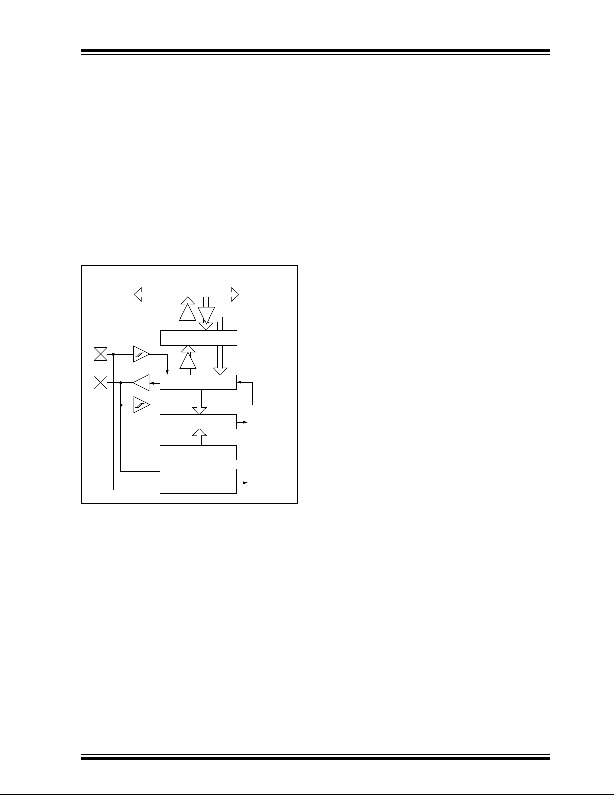
PIC16C9XX
11.3 SSP I2C Operation
The SSP module in I2C mode fully implements all slave
functions, except general call support, and provides
interrupts on start and stop bits in hardware to facilitate
firmware implementations of the master functions. The
SSP module implements the standard mode specifications as well as 7-bit and 10-bit addressing. Two pins
are used for data transfer . These are the RC3/SCK/SCL
pin, which is the clock (SCL), and the RC4/SDI/SDA
pin, which is the data (SDA). The user must configure
these pins as inputs or outputs through the
TRISC<4:3> bits. The SSP module functions are
enabled by setting SSP Enable bit SSPEN (SSPCON<5>).
FIGURE 11-18: SSP BLOCK DIAGRAM
(I2C MODE)
Internal
data bus
Read Write
shift
MSb
SSPBUF reg
SSPSR reg
Match detect
SSPADD reg
Start and
Stop bit detect
LSb
Addr Match
Set, Reset
S, P bits
(SSPSTAT reg)
RC3/SCK/SCL
clock
RC4/
SDI/
SDA
The SSP module has five registers for I2C operation.
These are the:
• SSP Control Register (SSPCON)
• SSP Status Register (SSPSTAT)
• Serial Receive/Transmit Buffer (SSPBUF)
• SSP Shift Register (SSPSR) - Not directly accessible
• SSP Address Register (SSPADD)
The SSPCON register allows control of the I2C operation. Four mode selection bits (SSPCON<3:0>) allow
one of the following I
2
C Slave mode (7-bit address)
• I
2
• I
C Slave mode (10-bit address)
2
• I
C Slave mode (7-bit address), with start and
2
C modes to be selected:
stop bit interrupts enabled
2
• I
C Slave mode (10-bit address), with start and
stop bit interrupts enabled
2
• I
C Firmware controlled Master Mode, slave is
idle
2
Selection of any I
C mode, with the SSPEN bit set,
forces the SCL and SDA pins to be open drain, provided these pins are programmed to inputs by setting
the appropriate TRISC bits.
The SSPSTAT register gives the status of the data
transfer. This information includes detection of a ST ART
or STOP bit, specifies if the received byte was data or
address if the next byte is the completion of 10-bit
address, and if this will be a read or write data transfer.
The SSPSTAT register is read only.
The SSPBUF is the register to which transfer data is
written to or read from. The SSPSR register shifts the
data in or out of the device. In receive operations, the
SSPBUF and SSPSR create a doubled buffered
receiver. This allows reception of the next byte to begin
before reading the last byte of receiv ed data. When the
complete byte is received, it is transferred to the
SSPBUF register and flag bit SSPIF is set. If another
complete byte is received before the SSPBUF register
is read, a receiver overflow has occurred and bit
SSPOV (SSPCON<6>) is set and the byte in the
SSPSR is lost.
The SSPADD register holds the slave address. In 10-bit
mode, the user needs to write the high byte of the
address (1111 0 A9 A8 0). Following the high byte
address match, the low byte of the address needs to be
loaded (A7:A0).
1997 Microchip Technology Inc. DS30444E - page 73

PIC16C9XX
11.3.1 SLAVE MODE
In slave mode, the SCL and SDA pins must be config-
ured as inputs (TRISC<4:3> set). The SSP module will
override the input state with the output data when
required (slave-transmitter).
When an address is matched or the data transfer after
an address match is received, the hardware automatically will generate the acknowledge (A
then load the SSPBUF register with the received value
currently in the SSPSR register.
There are certain conditions that will cause the SSP
module not to give this A
(or both):
a) The buffer full bit BF (SSPSTAT<0>) was set
before the transfer was received.
b) The overflow bit SSPOV (SSPCON<6>) was set
before the transfer was received.
In this case, the SSPSR register value is not loaded into
the SSPBUF, but bit SSPIF (PIR1<3>) is set. Table 11-3
shows what happens when a data transfer byte is
received, given the status of bits BF and SSPOV. The
shaded cells show the condition where user software
did not properly clear the overflow condition. Flag bit BF
is cleared by reading the SSPBUF register while bit
SSPOV is cleared through software.
The SCL clock input must have a minimum high and
low time for proper operation. The high and lo w times of
2
the I
C specification as well as the requirement of the
SSP module is shown in timing parameter #100 and
parameter #101.
11.3.1.1 ADDRESSING
Once the SSP module has been enabled, it waits for a
START condition to occur. Following the START condition, the 8-bits are shifted into the SSPSR register. All
incoming bits are sampled with the rising edge of the
clock (SCL) line. The value of register SSPSR<7:1> is
compared to the value of the SSPADD register. The
CK pulse. These are if either
CK) pulse, and
address is compared on the falling edge of the eighth
clock (SCL) pulse. If the addresses match, and the BF
and SSPOV bits are clear, the following events occur:
a) The SSPSR register value is loaded into the
SSPBUF register.
b) The buffer full bit, BF is set.
c) An A
d) SSP interrupt flag bit, SSPIF (PIR1<3>) is set
In 10-bit address mode, two address bytes need to be
received by the slav e (Figure 11-10). The fiv e Most Significant bits (MSbs) of the first address byte specify if
this is a 10-bit address. Bit R/W
specify a write so the slave device will receive the second address byte. For a 10-bit address the first byte
would equal ‘1111 0 A9 A8 0 ’, where A9 and A8 are
the two MSbs of the address. The sequence of events
for a 10-bit address is as follows, with steps 7- 9 for
slave-transmitter:
1. Receive first (high) byte of Address (bits SSPIF,
2. Update the SSPADD register with second (low)
3. Read the SSPBUF register (clears bit BF) and
4. Receive second (low) byte of Address (bits
5. Update the SSPADD register with the first (high)
6. Read the SSPBUF register (clears bit BF) and
7. Receive repeated START condition.
8. Receive first (high) byte of Address (bits SSPIF
9. Read the SSPBUF register (clears bit BF) and
CK pulse is generated.
(interrupt is generated if enabled) - on the falling
edge of the ninth SCL pulse.
(SSPSTAT<2>) must
BF, and bit UA (SSPSTAT<1>) are set).
byte of Address (clears bit UA and releases the
SCL line).
clear flag bit SSPIF.
SSPIF, BF, and UA are set).
byte of Address, if match releases SCL line, this
will clear bit UA.
clear flag bit SSPIF.
and BF are set).
clear flag bit SSPIF.
TABLE 11-3: DATA TRANSFER RECEIVED BYTE ACTIONS
Status Bits as Data
Transfer is Received
BF SSPOV
0 0 Yes Yes Yes
1 0 No No Yes
1 1 No No Yes
0 1 No No Yes
DS30444E - page 74 1997 Microchip Technology Inc.
SSPSR
→ SSPBUF
Generate A
CK
Pulse
Set bit SSPIF
(SSP Interrupt occurs
if enabled)
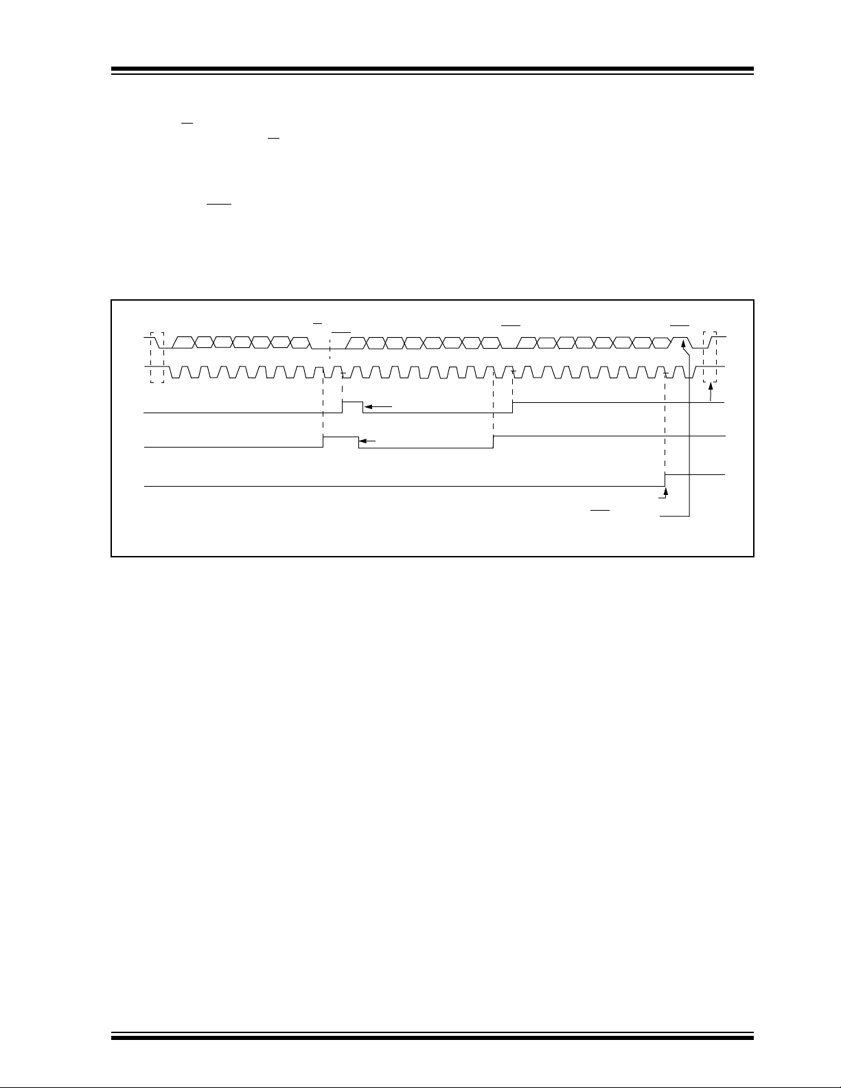
PIC16C9XX
11.3.1.2 RECEPTION
An SSP interrupt is generated for each data transfer
byte. Flag bit SSPIF (PIR1<3>) must be cleared in soft-
When the R/W
address match occurs, the R/W
bit of the address byte is clear and an
bit of the SSPST AT reg-
ware. The SSPSTAT register is used to determine the
status of the byte.
ister is cleared. The received address is loaded into the
SSPBUF register.
When the address byte overflow condition exists, then
no acknowledge (A
CK) pulse is given. An ov erflow condition is defined as either bit BF (SSPSTAT<0>) is set
or bit SSPOV (SSPCON<6>) is set.
FIGURE 11-19: I2C WAVEFORMS FOR RECEPTION (7-BIT ADDRESS)
Receiving Address
A7 A6 A5 A4
1 2
S
SCL
SSPIF (PIR1<3>)
BF (SSPSTAT<0>)
SSPOV (SSPCON<6>)
R/W=0
CK
A3 A2 A1SDA
3
6
4
5
A
7
9
8
Receiving Data
D5
D6D7
3
1 2
4
Cleared in software
SSPBUF register is read
Bit SSPOV is set because the SSPBUF register is still full.
D3D4
5 6
D2
D1
CK
A
D0
7
8 9
D6D7
1 2 3
Receiving Data
D5
D3D4
5
4
ACK is not sent.
D2
ACK
D0
D1
9
8
7
6
P
Bus Master
terminates
transfer
1997 Microchip Technology Inc. DS30444E - page 75

PIC16C9XX
11.3.1.3 TRANSMISSION
An SSP interrupt is generated for each data transfer
byte. Flag bit SSPIF must be cleared in software, and
When the R/W
and an address match occurs, the R/W
SSPSTAT register is set. The received address is
loaded into the SSPBUF register. The A
sent on the ninth bit, and pin RC3/SCK/SCL is held low .
The transmit data must be loaded into the SSPBUF
register, which also loads the SSPSR register . Then pin
RC3/SCK/SCL should be enabled by setting bit CKP
(SSPCON<4>). The master must monitor the SCL pin
prior to asserting another clock pulse. The slave
devices may be holding off the master b y stretching the
clock. The eight data bits are shifted out on the falling
edge of the SCL input. This ensures that the SD A signal
is valid during the SCL high time (Figure 11-20).
bit of the incoming address byte is set
bit of the
CK pulse will be
the SSPSTAT register is used to determine the status of
the byte. Flag bit SSPIF is set on the falling edge of the
ninth clock pulse.
As a slave-transmitter, the A
ter-receiver is latched on the rising edge of the ninth
SCL input pulse. If the SDA line was high (not A
then the data transfer is complete. When the A
latched by the slave, the slave logic is reset and the
slave then monitors for another occurrence of the
START bit. If the SDA line was low (A
data must be loaded into the SSPBUF register, which
also loads the SSPSR register. Then pin
RC3/SCK/SCL should be enabled by setting bit CKP.
FIGURE 11-20: I2C WAVEFORMS FOR TRANSMISSION (7-BIT ADDRESS)
SDA
SCL
SSPIF (PIR1<3>)
BF (SSPSTAT<0>)
CKP (SSPCON<4>)
A7 A6 A5 A4 A3 A2 A1 ACK D7 D6 D5 D4 D3 D2 D1 D0
1 2 3 4 5 6 7 8 9 1 2 3 4 5 6 7 8 9
S
Data in
sampled
SCL held low
while CPU
responds to SSPIF
cleared in software
SSPBUF is written in software
Set bit after writing to SSPBUF
(the SSPBUF must be written-to
before the CKP bit can be set)
CK pulse from the mas-
CK),
CK is
CK), the transmit
A
CKTransmitting DataR/W = 1Receiving Address
P
From SSP interrupt
service routine
DS30444E - page 76 1997 Microchip Technology Inc.
PIC16C9XX
11.3.2 MASTER MODE
Master mode of operation is supported, in firmware,
using interrupt generation on the detection of the
START and STOP conditions. The STOP (P) and
START (S) bits are cleared from a reset or when the
SSP module is disabled. The STOP and START bits will
toggle based on the start and stop conditions. Control
2
of the I
C bus may be taken when the P bit is set, or the
bus is idle with both the S and P bits clear.
In master mode the SCL and SDA lines are manipu-
lated by clearing the corresponding TRISC<4:3> bit(s).
The output level is always low, irrespective of the
value(s) in PORTC<4:3>. So when transmitting data, a
'1' data bit must have the TRISC<4> bit set (input) and
a '0' data bit must have the TRISC<4> bit cleared (output). The same scenario is true for the SCL line with the
TRISC<3> bit.
The following events will cause SSP Interrupt Flag bit,
SSPIF, to be set (SSP Interrupt if enabled):
• START condition
• STOP condition
• Data transfer byte transmitted/received
Master mode of operation can be done with either the
slave mode idle (SSPM3:SSPM0 = 1011) or with the
slave active. When both master and slave modes are
enabled, the software needs to differentiate the
source(s) of the interrupt.
11.3.3 MULTI-MASTER MODE
In multi-master mode, the interrupt generation on the
detection of the ST ART and ST OP conditions allows the
determination of when the bus is free. The STOP (P)
and START (S) bits are cleared from a reset or when
the SSP module is disabled. The ST OP and START bits
will toggle based on the start and stop conditions. Control of the I
2
C bus may be taken when bit P (SSPSTAT<4>) is set, or the bus is idle with both the S and
P bits clear. When the bus is busy, enabling the SSP
Interrupt will generate the interrupt when the STOP
condition occurs.
In multi-master operation, the SDA line must be monitored to see if the signal level is the expected output
level. This check only needs to be done when a high
level is output. If a high le v el is expected and a lo w lev el
is present, the device needs to release the SDA and
SCL lines (set TRISC<4:3>). There are two stages
where this arbitration can be lost, they are:
• Address Transfer
• Data Transfer
When the slave logic is enabled, the sla ve continues to
receive. If arbitration was lost during the address transfer stage, communication to the device may be in
progress. If addressed an A
CK pulse will be generated.
If arbitration was lost during the data transfer stage, the
device will need to re-transfer the data at a later time.
TABLE 11-4: REGISTERS ASSOCIATED WITH I2C OPERATION
Address Name Bit 7 Bit 6 Bit 5 Bit 4 Bit 3 Bit 2 Bit 1 Bit 0
0Bh, 8Bh,
10Bh, 18Bh
0Ch PIR1
8Ch PIE1
13h SSPBUF Synchronous Serial Port Receive Buffer/Transmit Register
93h SSPADD Synchronous Serial Port (I
14h SSPCON WCOL SSPOV SSPEN CKP SSPM3 SSPM2 SSPM1 SSPM0
94h SSPSTAT SMP CKE D/A
87h TRISC
Legend: x = unknown, u = unchanged, - = unimplemented read as '0'. Shaded cells are not used by SSP in I
Note 1: Bits ADIE and ADIF are reserved on the PIC16C923, always maintain these bits clear.
INTCON GIE PEIE
LCDIF ADIF
LCDIE ADIE
— — PORTC Data Direction Control Register
T0IE INTE RBIE T0IF INTF RBIF
(1)
— — SSPIF CCP1IF TMR2IF TMR1IF
(1)
— — SSPIE CCP1IE TMR2IE TMR1IE
2
C mode) Address Register
P S R/W UA BF
Value on
Power-on
Reset
0000 000x 0000 000u
00-- 0000 00-- 0000
00-- 0000 00-- 0000
xxxx xxxx uuuu uuuu
0000 0000 0000 0000
0000 0000 0000 0000
0000 0000 0000 0000
--11 1111 --11 1111
2
C mode.
Value on all
other resets
1997 Microchip Technology Inc. DS30444E - page 77

PIC16C9XX
FIGURE 11-21: OPERATION OF THE I2C MODULE IN IDLE_MODE, RCV_MODE OR XMIT_MODE
IDLE_MODE (7-bit):
if (Addr_match) { Set interrupt;
if (R/W
= 1) { Send ACK = 0;
set XMIT_MODE;
}
else if (R/W
}
RCV_MODE:
if ((SSPBUF=Full) OR (SSPOV = 1))
{ Set SSPOV;
Do not acknowledge;
}
else { transfer SSPSR → SSPBUF;
send A
CK = 0;
}
Receive 8-bits in SSPSR;
Set interrupt;
XMIT_MODE:
While ((SSPBUF = Empty) AND (CKP=0)) Hold SCL Low;
Send byte;
Set interrupt;
if ( A
CK Received = 1) { End of transmission;
Go back to IDLE_MODE;
}
else if ( A
IDLE_MODE (10-Bit):
If (High_byte_addr_match AND (R/W
else if (High_byte_addr_match AND (R/W
CK Received = 0) Go back to XMIT_MODE;
= 0))
{ PRIOR_ADDR_MATCH = FALSE;
Set interrupt;
if ((SSPBUF = Full) OR ((SSPOV = 1))
{ Set SSPOV;
Do not acknowledge;
}
else { Set UA = 1;
Send A
CK = 0;
While (SSPADD not updated) Hold SCL low;
Clear UA = 0;
Receive Low_addr_byte;
Set interrupt;
Set UA = 1;
If (Low_byte_addr_match)
{ PRIOR_ADDR_MATCH = TRUE;
}
}
}
= 1)
{ if (PRIOR_ADDR_MATCH)
{ send A
}
else PRIOR_ADDR_MATCH = FALSE;
}
CK = 0;
set XMIT_MODE;
= 0) set RCV_MODE;
Send A
CK = 0;
while (SSPADD not updated) Hold SCL low;
Clear UA = 0;
Set RCV_MODE;
DS30444E - page 78 1997 Microchip Technology Inc.

PIC16C9XX
12.0 ANALOG-TO-DIGITAL
CONVERTER (A/D) MODULE
This section applies to the PIC16C924 only.
The analog-to-digital (A/D) converter module has five
inputs.
The A/D allows conversion of an analog input signal to
a corresponding 8-bit digital number (refer to Application Note AN546 for use of A/D Converter). The output
of the sample and hold is the input into the converter,
which generates the result via successive approximation. The analog reference voltage is software selectable to either the device’s A
on the RA3/AN3/V
unique feature of being able to operate while the de vice
is in SLEEP mode.
To operate in sleep, the A/D conversion clock must be
derived from the A/D’s internal RC oscillator.
REF pin. The A/D converter has a
VDD pin or the voltage level
The A/D module has three registers. These registers
are:
• A/D Result Register (ADRES)
• A/D Control Register 0 (ADCON0)
• A/D Control Register 1 (ADCON1)
The ADCON0 register, shown in Figure 12-1, controls
the operation of the A/D module. The ADCON1 register, shown in Figure 12-2, configures the functions of
the port pins. The port pins can be configured as analog inputs (RA3 can also be a voltage reference) or as
digital I/O.
FIGURE 12-1: ADCON0 REGISTER (ADDRESS 1Fh)
R/W-0 R/W-0 R/W-0 R/W-0 R/W-0 R/W-0 R/W-0 R/W-0
ADCS1 ADCS0 CHS2 CHS1 CHS0 GO/DONE
bit7 bit0
bit 7-6: ADCS1:ADCS0: A/D Conversion Clock Select bits
00 = F
OSC/2
01 = F
OSC/8
10 = F
OSC/32
11 = F
RC (clock derived from an RC oscillation)
bit 5-3: CHS2:CHS0: Analog Channel Select bits
000 = channel 0, (RA0/AN0)
001 = channel 1, (RA1/AN1)
010 = channel 2, (RA2/AN2)
011 = channel 3, (RA3/AN3)
100 = channel 4, (RA5/AN4)
bit 2: GO/DONE
If ADON = 1
1 = A/D conversion in progress (setting this bit starts the A/D conversion)
0 = A/D conversion not in progress (This bit is automatically cleared b y hardware when the A/D conversion
is complete)
bit 1: Reserved: Always maintain this bit clear
bit 0: ADON: A/D On bit
1 = A/D converter module is operating
0 = A/D converter module is shutoff and consumes no operating current
: A/D Conversion Status bit
— ADON R =Readable bit
W =Writable bit
U =Unimplemented bit,
read as ‘0’
- n = Value at POR reset
1997 Microchip Technology Inc. DS30444E - page 79

PIC16C9XX
FIGURE 12-2: ADCON1 REGISTER (ADDRESS 9Fh)
U-0 U-0 U-0 U-0 U-0 R/W-0 R/W-0 R/W-0
— — — — — PCFG2 PCFG1 PCFG0 R =Readable bit
bit7 bit0
bit 7-3: Unimplemented: Read as '0'
bit 2-0: PCFG2:PCFG0: A/D Port Configuration Control bits
W =Writable bit
U =Unimplemented
- n = Value at POR reset
bit, read as ‘0’
PCFG2:PCFG0 RA0 RA1 RA2 RA5 RA3 V
000 A A A A A AVDD
001 A A A A VREF RA3
010 A A A A A A
011 A A A A VREF RA3
100 A A D D A A
111 D D D D D —
A = Analog input
D = Digital I/O
The ADRES register contains the result of the A/D conversion. When the A/D conversion is complete, the
result is loaded into the ADRES register, the GO/DONE
bit (ADCON0<2>) is cleared, and A/D interrupt flag bit
ADIF is set. The block diagram of the A/D module is
shown in Figure 12-3.
After the A/D module has been configured as desired,
the selected channel must be acquired before the conversion is started. The analog input channels must
have their corresponding TRIS bits selected as an
input. To determine acquisition time, see Section 12.1.
After this acquisition time has elapsed the A/D conversion can be started. The following steps should be followed for doing an A/D conversion:
1. Configure the A/D module:
• Configure analog pins / voltage reference /
and digital I/O (ADCON1)
• Select A/D input channel (ADCON0)
• Select A/D conversion clock (ADCON0)
• Turn on A/D module (ADCON0)
2. Configure A/D interrupt (if desired):
• Clear ADIF bit
• Set ADIE bit
• Set GIE bit
REF
VDD
VDD
3. Wait the required acquisition time.
4. Start conversion:
• Set GO/DONE
5. Wait for A/D conversion to complete, by either:
• Polling for the GO/DONE
OR
• Waiting for the A/D interrupt
6. Read A/D Result register (ADRES), clear bit
ADIF if required.
7. For next conversion, go to step 1 or step 2 as
required. The A/D conversion time per bit is
defined as T
required before next acquisition starts.
bit (ADCON0)
bit to be cleared
AD. A minimum wait of 2TAD is
DS30444E - page 80 1997 Microchip Technology Inc.

FIGURE 12-3: A/D BLOCK DIAGRAM
PIC16C9XX
CHS2:CHS0
A/D
Converter
VREF
(Reference
voltage)
VAIN
(Input voltage)
PCFG2:PCFG0
A
VDD
000 or
010 or
100
001 or
011
100
011
010
001
000
RA5/AN4
RA3/AN3/V
RA2/AN2
RA1/AN1
RA0/AN0
REF
1997 Microchip Technology Inc. DS30444E - page 81

PIC16C9XX
12.1 A/D Acquisition Requirements
For the A/D converter to meet its specified accuracy,
the charge holding capacitor (C
HOLD) must be allowed
to fully charge to the input channel voltage level. The
analog input model is shown in Figure 12-4. The source
impedance (R
S) and the internal sampling switch (RSS)
impedance directly affect the time required to charge
the capacitor C
ance varies over the device voltage (V
HOLD. The sampling s witch (RSS) imped-
DD),
(Figure 12-4). The source impedance affects the offset
voltage at the analog input (due to pin leakage current).
The maximum recommended impedance for analog sources is 10 kΩ . After the analog input channel is
selected (changed) this acquisition must be done
before the conversion can be started.
To calculate the minimum acquisition time,
Equation 12-1 may be used. This equation calculates
the acquisition time to within 1/2 LSb error (512 steps
for the A/D). The 1/2 LSb error is the maximum error
allowed for the A/D to meet its specified accuracy.
EQUATION 12-1: A/D MINIMUM CHARGING
TIME
VHOLD = (VREF - (VREF/512)) • (1 - e
Given: VHOLD = (VREF/512), for 1/2 LSb resolution
The above equation reduces to:
TC = -(51.2 pF)(1 kΩ - RSS + RS) ln(1/511)
Example 12-1 shows the calculation of the minimum
required acquisition time (T
based on the following system assumptions.
CHOLD = 51.2 pF
Rs = 10 k
Ω
1/2 LSb error
DD = 5V → Rss = 7 kΩ
V
Temp (system max.) = 50°C
HOLD = 0 @ t = 0
V
(-Tc/CHOLD(RIC + RSS + RS))
ACQ). This calculation is
Note 1: The reference voltage (VREF) has no
effect on the equation, since it cancels
itself out.
Note 2: The charge holding capacitor (C
HOLD) is
not discharged after each conversion.
Note 3: The maximum recommended impedance
for analog sources is 10 kΩ. This is
required to meet the pin leakage specification.
Note 4: After a conversion has completed, a
2.0 T
AD delay must complete before
acquisition can begin again. During this
time the holding capacitor is not connected to the selected A/D input channel.
EXAMPLE 12-1: CALCULATING THE
MINIMUM REQUIRED
SAMPLE TIME
TACQ = Amplifier Settling Time +
Holding Capacitor Charging Time +
Temperature Coefficient
ACQ = 5 µs + Tc + [(Temp - 25°C)(0.05 µs/°C)]
)
T
C = -CHOLD (RIC + RSS + RS) ln(1/511)
T
-51.2 pF (1 kΩ + 7 kΩ + 10 kΩ) ln(0.0020)
-51.2 pF (18 kΩ) ln(0.0020)
-0.921 µs (-6.2364)
5.747 µs
ACQ = 5 µs + 5.747 µs + [(50°C - 25°C)(0.05 µs/°C)]
T
10.747 µs + 1.25 µs
11.997 µs
FIGURE 12-4: ANALOG INPUT MODEL
VDD
RAx
Rs
VT
I leakage
IC
R
SS
C
HOLD
CPIN
5 pF
= input capacitance
= threshold voltage
= leakage current at the pin due to
various junctions
= interconnect resistance
= sampling switch
= sample/hold capacitance (from DAC)
VA
Legend CPIN
DS30444E - page 82 1997 Microchip Technology Inc.
VT = 0.6V
V
T = 0.6V
IC ≤ 1k
R
I leakage
± 500 nA
Sampling
Switch
SS
6V
5V
V
DD
4V
3V
2V
SS
R
CHOLD
= DAC capacitance
= 51.2 pF
SS
V
5 6 7 8 9 10 11
Sampling Switch
( kΩ )

PIC16C9XX
12.2 Selecting the A/D Conversion Clock
The A/D conversion time per bit is defined as TAD. The
A/D conversion requires 9.5 T
The source of the A/D conversion clock is software
selected. The four possible options for T
OSC
• 2T
• 8TOSC
• 32TOSC
• Internal RC oscillator
AD per 8-bit conversion.
AD are:
12.3 Configuring Analog Port Pins
The ADCON1 and TRISA registers control the operation of the A/D port pins. The port pins that are desired
as analog inputs must have their corresponding TRIS
bits set (input). If the TRIS bit is cleared (output), the
digital output level (V
The A/D operation is independent of the state of the
CHS2:CHS0 bits and the TRIS bits.
Note 1: When reading the port register, all pins
For correct A/D conversions, the A/D conversion clock
(T
AD) must be selected to ensure a minimum TAD time
of 1.6 µs.
Table 12-1 shows the resultant T
AD times derived from
the device operating frequencies and the A/D clock
source selected.
Note 2: Analog levels on any pin that is defined as
TABLE 12-1: TAD vs. DEVICE OPERATING FREQUENCIES
A/D Clock Source (TAD) Device Frequency
OH or VOL) will be converted.
configured as analog inputs will read as
cleared (a low level). Pins configured as
digital inputs, will convert an analog input.
Analog levels on a digitally configured
input will not affect the conversion accuracy.
a digital input (including the AN4:AN0
pins), may cause the input buffer to consume current that is out of the devices
specification.
Operation ADCS1:ADCS0 8 MHz 5 MHz 1.25 MHz 333.33 kHz
OSC 00 250 ns
2T
OSC 01 1 µs 1.6 µs 6.4 µs 24 µs
8T
(2)
32TOSC 10 4 µs 6.4 µs 25.6 µs
RC 11 2 - 6 µs
(1,4)
2 - 6 µs
400 ns
(2)
(1,4)
1.6 µs 6 µs
(3)
(1,4)
2 - 6 µs
96 µs
2 - 6 µs
(3)
(3)
(1)
Legend: Shaded cells are outside of recommended range.
Note 1: The RC source has a typical T
2: These values violate the minimum required T
AD time of 4 µs.
AD time.
3: For faster conversion times, the selection of another clock source is recommended.
4: When derived frequency is greater than 1 MHz, the RC A/D conversion clock source is recommended for
sleep mode only
5: For extended voltage devices (LC), please refer to the electrical specifications section.
1997 Microchip Technology Inc. DS30444E - page 83

PIC16C9XX
12.4 A/D Conversions
Example 12-2 show how to perform an A/D conv ersion.
The RA pins are configured as analog inputs. The analog reference (V
rupt is enabled, and the A/D conversion clock is F
The conversion is performed on the RA0 pin
(channel0).
Note: The GO/DONE bit should NOT be set in
REF) is the device VDD. The A/D inter-
RC.
the same instruction that turns on the A/D.
Clearing the GO/DONE bit during a conversion will
abort the current conversion. The ADRES register will
NOT be updated with the partially completed A/D conversion sample. That is, the ADRES register will continue to contain the value of the last completed
conversion (or the last value written to the ADRES register). After the A/D conversion is aborted, a 2T
is required before the next acquisition is started. After
this 2T
AD wait, an acquisition is automatically started on
the selected channel.
EXAMPLE 12-2: DOING AN A/D CONVERSION
BCF STATUS, RP1 ; Select Bank1
BSF STATUS, RP0 ;
CLRF ADCON1 ; Configure A/D inputs
BSF PIE1, ADIE ; Enable A/D interrupts
BCF STATUS, RP0 ; Select Bank0
MOVLW 0xC1 ; RC Clock, A/D is on, Channel 0 is selected
MOVWF ADCON0 ;
BCF PIR1, ADIF ; Clear A/D interrupt flag bit
BSF INTCON, PEIE ; Enable peripheral interrupts
BSF INTCON, GIE ; Enable all interrupts
;
; Ensure that the required acquisition time for the selected input channel has elapsed.
; Then the conversion may be started.
;
BSF ADCON0, GO ; Start A/D Conversion
: ; The ADIF bit will be set and the GO/DONE bit
: ; is cleared upon completion of the A/D Conversion.
AD wait
DS30444E - page 84 1997 Microchip Technology Inc.

PIC16C9XX
12.4.1 FASTER CONVERSION - LOWER
RESOLUTION TRADE-OFF
Since the T
AD is based from the device oscillator, the
user must use some method (a timer, software loop,
etc.) to determine when the A/D oscillator may be
Not all applications require a result with 8-bits of resolution, but may instead require a f aster conv ersion time.
The A/D module allows users to make the trade-off of
conversion speed to resolution. Regardless of the resolution required, the acquisition time is the same. To
speed up the conversion, the clock source of the A/D
module may be switched so that the T
AD time violates
the minimum specified time (see the applicable electrical specification). Once the T
AD time violates the mini-
changed. Example 12-3 shows a comparison of time
required for a conversion with 4-bits of resolution, versus the 8-bit resolution conversion. The example is for
devices operating at 8 MHz (The A/D clock is programmed for 32T
after 6T
The 2T
AD, the A/D clock is programmed for 2TOSC.
OSC violates the minimum TAD time, therefore
OSC), and assumes that immediately
the last 4-bits will not be converted to correct values.
mum specified time, all the following A/D result bits are
not valid (see A/D Conversion Timing in the Electrical
Specifications section.) The clock sources may only be
switched between the three oscillator versions (cannot
be switched from/to RC). The equation to determine
the time before the oscillator can be switched is as follows:
Conversion time = 2T
AD + N • TAD + (8 - N)(2TOSC)
Where: N = number of bits of resolution required.
EXAMPLE 12-3: 4-BIT vs. 8-BIT CONVERSION TIMES
Freq. (MHz)
TAD 8 1.6 µs 1.6 µs
OSC 8 12.5 ns 125 ns
T
AD + N • TAD + (8 - N)(2TOSC) 8 10.6 µs 16 µs
2T
Resolution
4-bit 8-bit
1997 Microchip Technology Inc. DS30444E - page 85

PIC16C9XX
12.5 A/D Operation During Sleep
The A/D module can operate during SLEEP mode. This
requires that the A/D clock source be set to RC
(ADCS1:ADCS0 = 11). When the RC clock source is
selected, the A/D module waits one instruction cycle
before starting the conversion. This allows the SLEEP
instruction to be executed, which eliminates all digital
switching noise from the conversion. When the conversion is completed the GO/DONE
the result loaded into the ADRES register. If the A/D
interrupt is enabled, the device will wake-up from
SLEEP. If the A/D interrupt is not enabled, the A/D module will then be turned off, although the ADON bit will
remain set.
When the A/D clock source is another clock option (not
RC), a SLEEP instruction will cause the present conversion to be aborted and the A/D module to be turned off,
though the ADON bit will remain set.
Turning off the A/D places the A/D module in its lowest
current consumption state.
Note: For the A/D module to operate in SLEEP,
the A/D clock source must be set to RC
(ADCS1:ADCS0 = 11). To perform an A/D
conversion in SLEEP, ensure the SLEEP
instruction immediately follows the instruction that sets the GO/DONE
bit will be cleared, and
bit.
12.6 A/D Accuracy/Error
The absolute accuracy specified for the A/D converter
includes the sum of all contributions for quantization
error, integral error , diff erential error , full scale error, offset error, and monotonicity. It is defined as the maximum deviation from an actual transition versus an ideal
transition for any code. The absolute error of the A/D
converter is specified at < ±1 LSb for V
the device’s specified operating range). However, the
accuracy of the A/D converter will degrade as V
diverges from VREF.
For a given range of analog inputs, the output digital
code will be the same. This is due to the quantization of
the analog input to a digital code. Quantization error is
typically ± 1/2 LSb and is inherent in the analog to digital conversion process. The only way to reduce quantization error is to increase the resolution of the A/D
converter.
Offset error measures the first actual transition of a
code versus the first ideal transition of a code. Offset
error shifts the entire transfer function. Offset error can
be calibrated out of a system or introduced into a system through the interaction of the total leakage current
and source impedance at the analog input.
Gain error measures the maximum deviation of the last
actual transition and the last ideal transition adjusted for
offset error. This error appears as a change in slope of
the transfer function. The difference in gain error to full
DD = VREF (over
DD
scale error is that full scale does not take offset error
into account. Gain error can be calibrated out in software.
Linearity error refers to the uniformity of the code
changes. Linearity errors cannot be calibrated out of
the system. Integral non-linearity error measures the
actual code transition versus the ideal code transition
adjusted by the gain error for each code.
Differential non-linearity measures the maximum actual
code width versus the ideal code width. This measure
is unadjusted.
The maximum pin leakage current is ± 1 µA.
In systems where the device frequency is low, use of
the A/D RC clock is preferred. At moderate to high frequencies, T
lator. T
≤ 8 µs for preferred operation. This is because T
when derived from T
phase clock transitions. This reduces, to a large extent,
the effects of digital switching noise . This is not possib le
with the RC derived clock. The loss of accuracy due to
digital switching noise can be significant if many I/O
pins are active.
In systems where the device will enter SLEEP mode
after the start of the A/D conversion, the RC clock
source selection is required. In this mode, the digital
noise from the modules in SLEEP are stopped. This
method gives high accuracy.
AD should be derived from the device oscil-
AD must not violate the minimum and should be
AD,
OSC, is kept away from on-chip
12.7 Effects of a RESET
A device reset forces all registers to their reset state.
This forces the A/D module to be turned off, and any
conversion is aborted.
The value that is in the ADRES register is not modified
for a Power-on Reset. The ADRES register will contain
unknown data after a Power-on Reset.
DS30444E - page 86 1997 Microchip Technology Inc.

PIC16C9XX
12.8 Use of the CCP Trigger
An A/D conversion can be started by the “special e v ent
trigger” of the CCP1 module. This requires that the
CCP1M3:CCP1M0 bits (CCP1CON<3:0>) be programmed as 1011 and that the A/D module is enabled
(ADON bit is set). When the trigger occurs, the
GO/DONE
bit will be set, starting the A/D conversion,
and the Timer1 counter will be reset to zero. Timer1 is
reset to automatically repeat the A/D acquisition period
with minimal software overhead (moving the ADRES to
the desired location). The appropriate analog input
channel must be selected and the minimum acquisition
done before the “special event trigger” sets the
GO/DONE
bit (starts a conversion).
If the A/D module is not enabled (ADON is cleared),
then the “special event trigger” will be ignored by the
A/D module, but will still reset the Timer1 counter.
12.9 Connection Considerations
If the input voltage exceeds the rail v alues (VSS or VDD)
by greater than 0.2V, then the accuracy of the conversion is out of specification.
An external RC filter is sometimes added for anti-aliasing of the input signal. The R component should be
selected to ensure that the total source impedance is
kept under the 10 kΩ recommended specification. Any
external components connected (via hi-impedance) to
an analog input pin (capacitor, zener diode , etc.) should
have very little leakage current at the pin.
12.10 Transfer Function
The ideal transfer function of the A/D conv erter is as follows: the first transition occurs when the analog input
voltage (V
AIN) is Analog VREF / 256 (Figure 12-5).
FIGURE 12-5: A/D TRANSFER FUNCTION
FFh
FEh
04h
Digital code output
03h
02h
01h
00h
1 LSb
2 LSb
3 LSb
0.5 LSb
4 LSb
Analog input voltage
255 LSb
256 LSb
(full scale)
1997 Microchip Technology Inc. DS30444E - page 87

PIC16C9XX
FIGURE 12-6: FLOWCHART OF A/D OPERATION
ADON = 0
ADON = 0?
No
Acquire
Selected Channel
GO = 0?
No
A/D Clock
= RC?
No
Device in
SLEEP?
No
Finish Conversion
GO = 0
ADIF = 1
Yes
Yes
Yes
Yes
Start of A/D
Conversion Delayed
1 Instruction Cycle
Abort Conversion
GO = 0
ADIF = 0
SLEEP
Power-down A/D
SLEEP
Instruction?
No
Finish Conversion
GO = 0
ADIF = 1
Wait 2 T
AD
Yes
Finish Conversion
GO = 0
ADIF = 1
Wake-up
From Sleep?
No
Stay in Sleep
Power-down A/D
Yes
Wait 2 TAD
Wait 2 TAD
TABLE 12-2: SUMMARY OF A/D REGISTERS
Address Name Bit 7 Bit 6 Bit 5 Bit 4 Bit 3 Bit 2 Bit 1 Bit 0
0Bh, 8Bh,
INTCON GIE PEIE
10Bh, 18Bh
0Ch PIR1 LCDIF ADIF — — SSPIF CCP1IF TMR2IF TMR1IF
8Ch PIE1
LCDIE ADIE — — SSPIE CCP1IE TMR2IE TMR1IE
1Eh ADRES A/D Result Register
1Fh ADCON0 ADCS1 ADCS0 CHS2 CHS1 CHS0 GO/DONE
9Fh ADCON1 — — — — — PCFG2 PCFG1 PCFG0
05h PORTA
85h TRISA
— — RA5 RA4 RA3 RA2 RA1 RA0
— — PORTA Data Direction Control Register
Legend: x = unknown, u = unchanged, - = unimplemented read as '0'. Shaded cells are not used for A/D conversion.
Note 1: Bit1 of ADCON0 is reserved, always maintain this bit clear.
T0IE INTE RBIE T0IF INTF RBIF
(1)
ADON
Value on
Power-on
Reset
Value on all
other Resets
0000 000x 0000 000u
00-- 0000 00-- 0000
00-- 0000 00-- 0000
xxxx xxxx uuuu uuuu
0000 0000 0000 0000
---- -000 ---- -000
--0x 0000 --0u 0000
--11 1111 --11 1111
DS30444E - page 88 1997 Microchip Technology Inc.

PIC16C9XX
13.0 LCD MODULE
The LCD module generates the timing control to drive
a static or multiplexed LCD panel, with support for up to
32 segments multiplexed with up to 4 commons . It also
provides control of the LCD pixel data.
The interface to the module consists of 3 control registers (LCDCON, LCDSE, and LCDPS) used to define
the timing requirements of the LCD panel and up to 16
LCD data registers (LCD00-LCD15) that represent the
array of the pixel data. In normal operation, the control
registers are configured to match the LCD panel being
used. Primarily, the initialization information consists of
selecting the number of commons required by the LCD
panel, and then specifying the LCD Frame cloc k rate to
be used by the panel.
Once the module is initialized for the LCD panel, the
individual bits of the LCD data registers are cleared/set
to represent a clear/dark pixel respectively.
Once the module is configured, the LCDEN
(LCDCON<7>) bit is used to enable or disable the LCD
module. The LCD panel can also operate during sleep
by clearing the SLPEN (LCDCON<6>) bit.
Figure 13-4 through Figure 13-7 provides waveforms
for Static, 1/2, 1/3, and 1/4 MUX drives.
FIGURE 13-1: LCDCON REGISTER (ADDRESS 10Fh)
R/W-0 R/W-0 U-0 R/W-0 R/W-0 R/W-0 R/W-0 R/W-0
LCDEN SLPEN
bit7 bit0
bit 7: LCDEN: Module drive enable bit
1 = LCD drive enabled
0 = LCD drive disabled
bit 6: SLPEN: LCD display sleep enable
1 = LCD module will stop operating during SLEEP
0 = LCD module will continue to display during SLEEP
bit 5: Unimplemented: Read as '0'
bit 4: VGEN: Voltage Generator Enable
1 = Internal LCD Voltage Generator Enabled, (powered-up)
0 = Internal LCD Voltage Generator powered-down, voltage is expected to be provided externally
bit 3-2: CS1:CS0: Clock Source Select bits
00 = Fosc/256
01 = T1CKI (Timer1)
1x = Internal RC oscillator
bit 1-0: LMUX1:LMUX0: Common Selection bits
Specifies the number of commons and the bias method
LMUX1:LMUX0 MULTIPLEX BIAS Max # of Segments
00
01
10
11
— VGEN CS1 CS0 LMUX1 LMUX0 R =Readable bit
Static (COM0)
1/2 (COM0, 1)
1/3 (COM0, 1, 2)
1/4 (COM0, 1, 2, 3)
Static
1/3
1/3
1/3
W =Writable bit
U =Unimplemented bit,
Read as ‘0’
-n =Value at POR reset
32
31
30
29
1997 Microchip Technology Inc. DS30444E - page 89
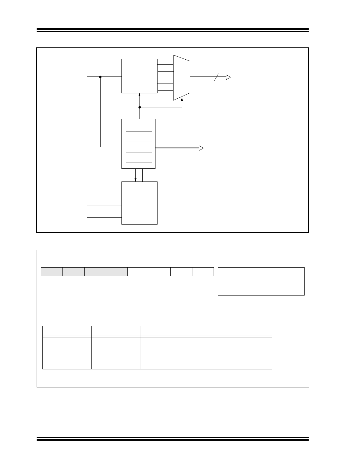
PIC16C9XX
FIGURE 13-2: LCD MODULE BLOCK DIAGRAM
Data Bus
Internal RC osc
T1CKI
Fosc/4
LCD
RAM
32 x 4
Timing Control
LCDCON
LCDPS
LCDSE
Clock
Source
Select
and
Divide
128
to
32
MUX
COM3:COM0
SEG<31:0>
TO I/O PADS
TO I/O PADS
FIGURE 13-3: LCDPS REGISTER (ADDRESS 10Eh)
U-0 U-0 U-0 U-0 R/W-0 R/W-0 R/W-0 R/W-0
— — — — LP3 LP2 LP1 LP0 R =Readable bit
bit7 bit0
bit 7-4: Unimplemented, read as '0'
bit 3-0: LP3:LP0: Frame Clock Prescale Selection bits
LMUX1:LMUX0 Multiplex Frame Frequency =
00 Static Clock source / (128 * (LP3:LP0 + 1))
01 1/2 Clock source / (128 * (LP3:LP0 + 1))
10 1/3 Clock source / (96 * (LP3:LP0 + 1))
11 1/4 Clock source / (128 * (LP3:LP0 + 1))
W =Writable bit
U =Unimplemented bit, Read as ‘0’
-n =Value at POR reset
DS30444E - page 90 1997 Microchip Technology Inc.

FIGURE 13-4: WAVEFORMS IN STATIC DRIVE
COM0
COM0
SEG0
SEG1
COM0-SEG0
COM0-SEG1
SEG1
SEG2
SEG4
SEG5
SEG7
SEG6
SEG3
SEG0
1 Frame
PIC16C9XX
V
1
V
0
V
1
V
0
V
1
V
0
V
1
V
0
-V
1
V
0
1997 Microchip Technology Inc. DS30444E - page 91

PIC16C9XX
FIGURE 13-5: WAVEFORMS IN 1/2 MUX, 1/3 BIAS DRIVE
COM0
COM1
COM0
COM1
SEG0
SEG0
SEG1
SEG2
SEG3
SEG1
V
3
V
2
V
1
V
0
V
3
V
2
V
1
V
0
V
3
V
2
V
1
V
0
V
3
V
2
V
1
V
0
COM0-SEG0
COM0-SEG1
1 Frame
V
3
V
2
V
1
V
0
-V
1
-V
2
-V
3
V
3
V
2
V
1
V
0
-V
1
-V
2
-V
3
DS30444E - page 92 1997 Microchip Technology Inc.
FIGURE 13-6: WAVEFORMS IN 1/3 MUX, 1/3 BIAS
COM0
COM2
COM1
COM1
COM0
COM2
SEG0
SEG2
SEG1
SEG0
SEG1
COM0-SEG0
COM0-SEG1
PIC16C9XX
V
3
V
2
V
1
V
0
V
3
V
2
V
1
V
0
V
3
V
2
V
1
V
0
V
3
V
2
V
1
V
0
V
3
V
2
V
1
V
0
V
3
V
2
V
1
V
0
-V
1
-V
2
-V
3
V
3
V
2
V
1
V
0
-V
1
-V
2
-V
3
1 Frame
1997 Microchip Technology Inc. DS30444E - page 93
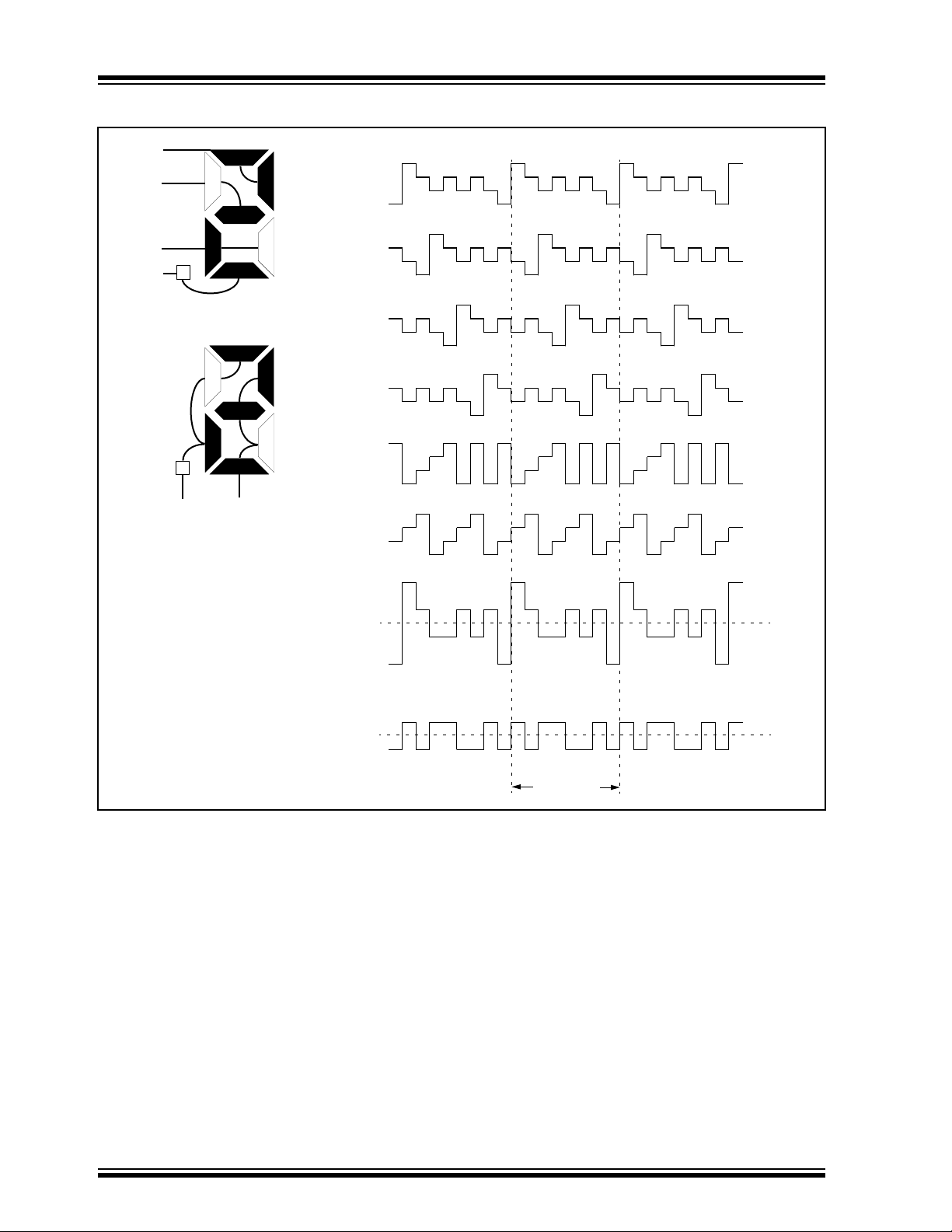
PIC16C9XX
FIGURE 13-7: WAVEFORMS IN 1/4 MUX, 1/3 BIAS
COM3
COM2
COM1
COM0
SEG1
SEG0
COM0
COM1
COM2
COM3
SEG0
SEG1
COM0-SEG0
V
3
V
2
V
1
V
0
V
3
V
2
V
1
V
0
V
3
V
2
V
1
V
0
V
3
V
2
V
1
V
0
V
3
V
2
V
1
V
0
V
3
V
2
V
1
V
0
V
3
V
2
V
1
V
0
-V
1
-V
2
-V
3
COM0-SEG1
1 Frame
V
3
V
2
V
1
V
0
-V
1
-V
2
-V
3
DS30444E - page 94 1997 Microchip Technology Inc.
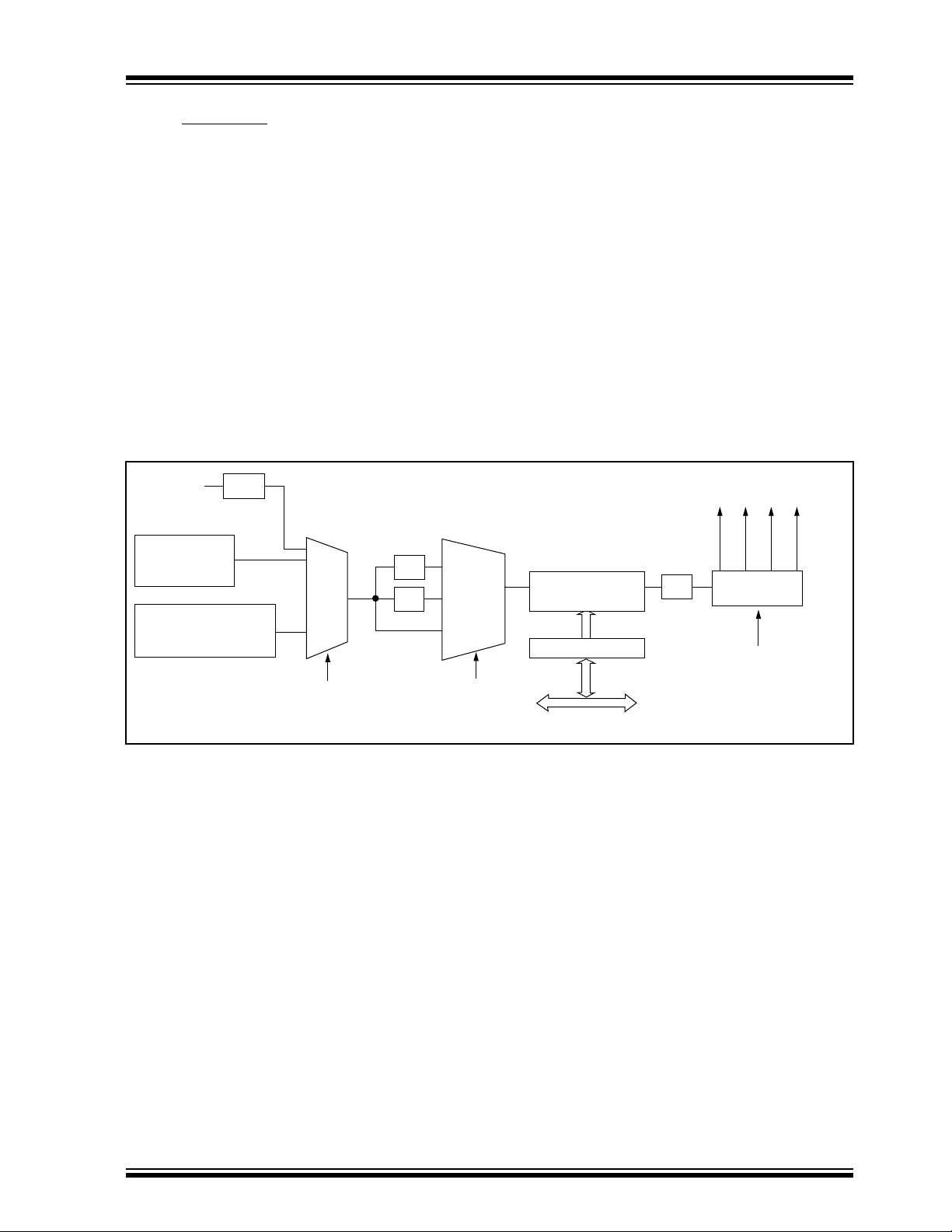
PIC16C9XX
13.1 LCD Timing
The LCD module has 3 possible clock source inputs
and supports static, 1/2, 1/3, and 1/4 multiplexing.
13.1.1 TIMING CLOCK SOURCE SELECTION
The clock sources for the LCD timing generation are:
• Internal RC oscillator
• Timer1 oscillator
• System clock divided by 256
The first timing source is an internal RC oscillator which
runs at a nominal frequency of 14 kHz. This oscillator
provides a lower speed clock which may be used to
continue running the LCD while the processor is in
sleep. The RC oscillator will pow er-do wn when it is not
selected or when the LCD module is disabled.
FIGURE 13-8: LCD CLOCK GENERATION
FOSC
TMR1 32 kHz
crystal oscillator
Internal RC oscillator
Nominal F
÷256
RC = 14 kHz
÷4
÷2
Static
1/2
1/3
1/4
The second source is the Timer1 external oscillator.
This oscillator provides a lower speed clock which ma y
be used to continue running the LCD while the processor is in sleep. It is assumed that the frequency provided on this oscillator will be 32 kHz. To use the
Timer1 oscillator as a LCD module clock source, it is
only necessary to set the T1OSCEN (T1CON<3>) bit.
The third source is the system clock divided by 256.
This divider ratio is chosen to provide about 32 kHz
output when the external oscillator is 8 MHz. The
divider is not programmable. Instead the LCDPS register is used to set the LCD frame clock rate.
All of the clock sources are selected with bits CS1:CS0
(LCDCON<3:2>). Ref er to Figure 13-1 for details of the
register programming.
COM1
÷1,2,3,4
COM2
COM3
4-bit Programmable
Prescaler
LCDPS<3:0>
÷32
COM0
Ring Counter
LMUX1:LMUX0
CS1:CS0
LMUX1:LMUX0
internal
data bus
1997 Microchip Technology Inc. DS30444E - page 95

PIC16C9XX
13.1.2 MULTIPLEX TIMING GENERATION
The timing generation circuitry will generate 1 to 4 com-
mon clocks based on the display mode selected. The
mode is specified by bits LMUX1:LMUX0
(LCDCON<1:0>). Table 13-1 shows the formulas for
calculating the frame frequency.
TABLE 13-1: FRAME FREQUENCY
FORMULAS
Multiplex Frame Frequency =
Static Clock source / (128 * (LP3:LP0 + 1))
1/2 Clock source / (128 * (LP3:LP0 + 1))
1/3 Clock source / (96 * (LP3:LP0 + 1))
1/4 Clock source / (128 * (LP3:LP0 + 1))
TABLE 13-2: APPROX. FRAME FREQ IN Hz
USING TIMER1 @ 32.768 kHz OR
Fosc @ 8 MHz
LP3:LP0 Static 1/2 1/3 1/4
2 85 85 114 85
3 64 64 85 64
4 51 51 68 51
5 43 43 57 43
6 37 37 49 37
7 32 32 43 32
TABLE 13-3: APPROX. FRAME FREQ IN Hz
USING INTERNAL RC OSC @
14 kHz
LP3:LP0 Static 1/2 1/3 1/4
0 109 109 146 109
1 55 55 73 55
2 36 36 49 36
3 27 27 36 27
DS30444E - page 96 1997 Microchip Technology Inc.

PIC16C9XX
13.2 LCD Interrupts
The LCD timing generation provides an interrupt that
defines the LCD frame timing. This interrupt can be
used to coordinate the writing of the pixel data with the
start of a new frame. Wr iting pixel data at the frame
boundary allows a visually crisp transition of the image.
This interrupt can also be used to synchronize external
events to the LCD. For example, the interface to an
external segment driver, such as a Microchip AY0438,
can be synchronized for segment data update to the
LCD frame.
A new frame is defined to begin at the leading edge of
the COM0 common signal. The interrupt will be set
immediately after the LCD controller completes
accessing all pixel data required for a frame. This will
occur at a certain fixed time before the frame boundary
as shown in Figure 13-9. The LCD controller will begin
to access data for the next frame within T
interrupt.
FIGURE 13-9: EXAMPLE WAVEFORMS IN 1/4 MUX DRIVE
LCD
Interrupt
occurs
COM0
FWR after the
Controller accesses
next frame data
V3
V2
V1
V0
COM1
COM2
COM3
Frame
Boundary
TFWR = TFRAME/(LMUX1:LMUX0 + 1)
FINT = (TFWR /2 - (2TCY + 40 ns)) → min.
T
(T
FWR /2 - (1TCY + 40 ns)) → max.
1 Frame
TFWR
V3
V2
V1
V0
V3
V2
V1
V0
V3
V2
V1
V0
TFINT
Frame
Boundary
1997 Microchip Technology Inc. DS30444E - page 97

PIC16C9XX
13.3 Pixel Control
13.3.1 LCDD (PIXEL DATA) REGISTERS
The pixel registers contain bits which define the state of
each pixel. Each bit defines one unique pixel.
Table 13-4 shows the correlation of each bit in the
LCDD registers to the respective common and segment signals.
Any LCD pixel location not being used for display can
be used as general purpose RAM.
FIGURE 13-10:GENERIC LCDD REGISTER LAYOUT
R/W-x R/W-x R/W-x R/W-x R/W-x R/W-x R/W-x R/W-x
SEGs
COMc
bit7 bit0
bit 7-0: SEGsCOMc: Pixel Data Bit for segment s and common c
SEGs
COMc
1 = Pixel on (dark)
0 = Pixel off (clear)
SEGs
COMc
SEGs
COMc
SEGs
COMc
SEGs
COMc
SEGs
COMc
SEGs
COMc
R =Readable bit
W =Writable bit
U =Unimplemented bit,
Read as ‘0’
-n =Value at POR reset
DS30444E - page 98 1997 Microchip Technology Inc.

PIC16C9XX
13.4 Operation During Sleep
The LCD interrupt can be used to determine the frame
boundary. See Section 13.2 for the formulas to calcu-
The LCD module can operate during sleep. The selection is controlled by bit SLPEN (LCDCON<6>). Setting
the SLPEN bit allows the LCD module to go to sleep.
Clearing the SLPEN bit allows the module to continue
to operate during sleep.
If a SLEEP instruction is executed and SLPEN = '1', the
LCD module will cease all functions and go into a very
low current consumption mode. The module will stop
operation immediately and drive the minimum LCD
voltage on both segment and common lines. Figure
13-11 shows this operation. To ensure that the LCD
late the delay.
If a SLEEP instruction is executed and SLPEN = '0', the
module will continue to display the current contents of
the LCDD registers. To allow the module to continue
operation while in sleep, the clock source must be
either the internal RC oscillator or Timer1 external
oscillator. While in sleep, the LCD data cannot be
changed. The LCD module current consumption will
not decrease in this mode, however the overall consumption of the device will be lower due to shutdown of
the core and other peripheral functions.
completes the frame, the SLEEP instruction should be
executed immediately after a LCD frame boundary.
Note: The internal RC oscillator or external
Timer1 oscillator must be used to operate
the LCD module during sleep.
FIGURE 13-11:SLEEP ENTRY/EXIT WHEN SLPEN = 1 OR CS1:CS0 = 00
Pin
COM0
3/3V
2/3V
1/3V
0/3V
Pin
COM1
Pin
COM3
Pin
SEG0
interrupted
frame
SLEEP instruction execution
3/3V
2/3V
1/3V
0/3V
3/3V
2/3V
1/3V
0/3V
3/3V
2/3V
1/3V
0/3V
Wake-up
1997 Microchip Technology Inc. DS30444E - page 99

PIC16C9XX
13.4.1 SEGMENT ENABLES
The LCDSE register is used to select the pin function
for groups of pins. The selection allows each group of
pins to operate as either LCD drivers or digital only
pins. To configure the pins as a digital por t, the corresponding bits in the LCDSE register must be cleared.
If the pin is a digital I/O the corresponding TRIS bit controls the data direction. Any bit set in the LCDSE register overrides any bit settings in the corresponding TRIS
register.
Note 1: On a Power-on Reset these pins are con-
figured as LCD drivers.
Note 2: The LMUX1:LMUX0 takes precedence
over the LCDSE bit settings for pins RD7,
RD6 and RD5.
EXAMPLE 13-1: STATIC MUX WITH 32
SEGMENTS
BCF STATUS,RP0 ;Select Bank 2
BSF STATUS,RP1 ;
BCF LCDCON,LMUX1 ;Select Static MUX
BCF LCDCON,LMUX0 ;
MOVLW 0xFF ;Make PortD,E,F,G
MOVWF LCDSE ;LCD pins
. . . ;configure rest of LCD
EXAMPLE 13-2: 1/3 MUX WITH 13
SEGMENTS
BCF STATUS,RP0 ;Select Bank 2
BSF STATUS,RP1 ;
BSF LCDCON,LMUX1 ;Select 1/3 MUX
BCF LCDCON,LMUX0 ;
MOVLW 0x87 ;Make PORTD<7:0> &
MOVWF LCDSE ;PORTE<6:0> LCD pins
. . . ;configure rest of LCD
FIGURE 13-12:LCDSE REGISTER (ADDRESS 10Dh)
R/W-1 R/W-1 R/W-1 R/W-1 R/W-1 R/W-1 R/W-1 R/W-1
SE29 SE27 SE20 SE16 SE12 SE9 SE5 SE0 R =Readable bit
bit7 bit0
bit 7: SE29: Pin function select RD7/COM1/SEG31 - RD5/COM3/SEG29
1 = pins have LCD drive function
0 = pins have digital Input function
The LMUX1:LMUX0 setting takes precedence over the LCDSE register.
bit 6: SE27: Pin function select RG7/SEG28 and RE7/SEG27
1 = pins have LCD drive function
0 = pins have digital Input function
bit 5: SE20: Pin function select RG6/SEG26 - RG0/SEG20
1 = pins have LCD drive function
0 = pins have digital Input function
bit 4: SE16: Pin function select RF7/SEG19 - RF4/SEG16
1 = pins have LCD drive function
0 = pins have digital Input function
bit 3: SE12: Pin function select RF3/SEG15 - RF0/SEG12
1 = pins have LCD drive function
0 = pins have digital Input function
bit 2: SE9: Pin function select RE6/SEG11 - RE4/SEG09
1 = pins have LCD drive function
0 = pins have digital Input function
bit 1: SE5: Pin function select RE3/SEG08 - RE0/SEG05
1 = pins have LCD drive function
0 = pins have digital Input function
bit 0: SE0: Pin function select RD4/SEG04 - RD0/SEG00
1 = pins have LCD drive function
0 = pins have digital I/O function
W =Writable bit
U =Unimplemented bit,
Read as ‘0’
-n =Value at POR reset
DS30444E - page 100 1997 Microchip Technology Inc.
 Loading...