

Microchip Technology Inc PIC16C773-I-SO, PIC16C773-I-SP, PIC16C773-JW, PIC16C774-I-L, PIC16C774-I-P Datasheet
...
1999 Microchip Technology Inc. Advance Information DS30275A-page 1
Microcontroller Core Features:
• High-performance RISC CPU
• Only 35 single word instructions to learn
• All single cycle instructions except for program
branches which are two cycle
• Operating speed: DC - 20 MHz clock input
DC - 200 ns instruction cycle
• 4K x 14 words of Program Memory,
256 x 8 bytes of Data Memory (RAM)
• Interrupt capability (up to 14 internal/external
interrupt sources)
• Eight level deep hardware stack
• Direct, indirect, and relative addressing modes
• Power-on Reset (POR)
• Power-up Timer (PWRT) and
Oscillator Start-up Timer (OST)
• Watchdog Timer (WDT) with its own on-chip RC
oscillator for reliable operation
• Programmable code-protection
• Power saving SLEEP mode
• Selectable oscillator options
• Low-power, high-speed CMOS EPROM
technology
• Fully static design
• In-Circuit Serial Programming (ISCP)
• Wide operating voltage range: 2.5V to 5.5V
• High Sink/Source Current 25/25 mA
• Commercial and Industrial temperature ranges
• Low-power consumption:
- < 2 mA @ 5V, 4 MHz
- 22.5 µA typical @ 3V, 32 kHz
-< 1 µA typical standby current
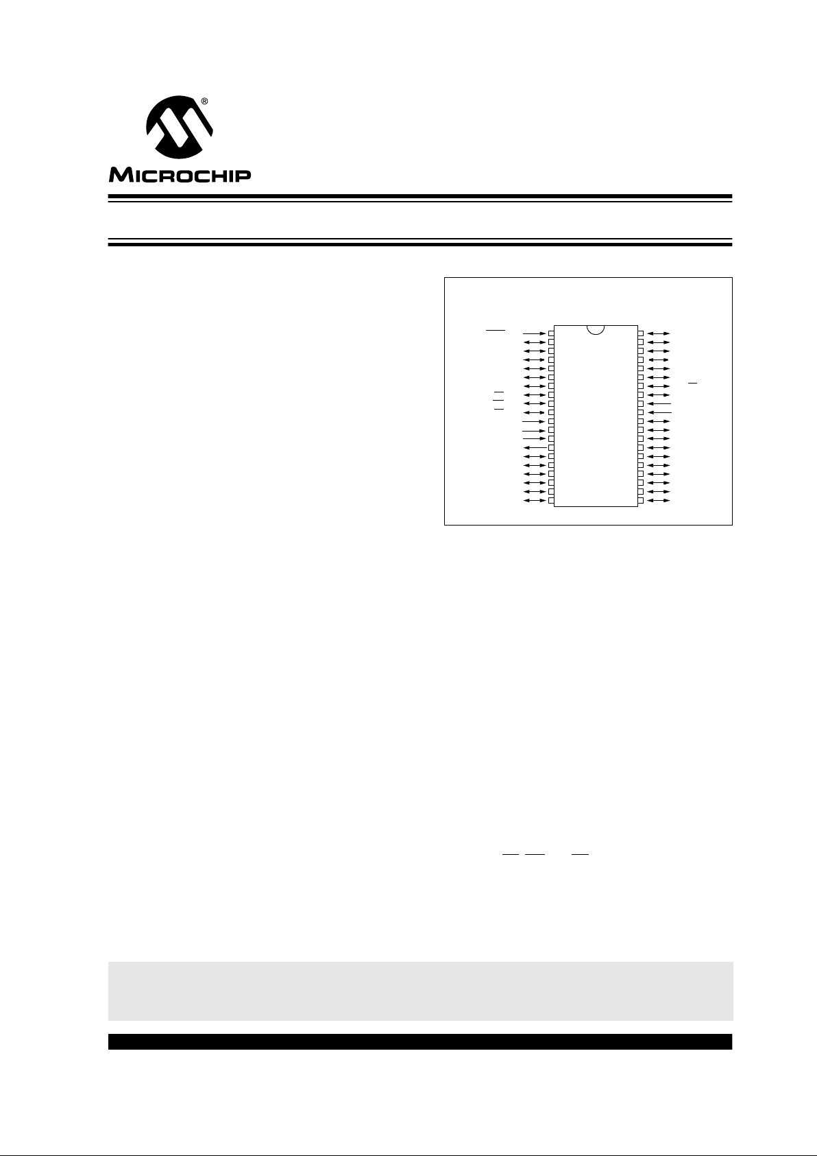
Pin Diagram
Peripheral Features:
• Timer0: 8-bit timer/counter with 8-bit prescaler
• Timer1: 16-bit timer/counter with prescaler,
can be incremented during sleep via external
crystal/clock
• Timer2: 8-bit timer/counter with 8-bit period
register, prescaler and postscaler
• Two Capture, Compare, PWM modules
• Capture is 16-bit, max. resolution is 12.5 ns,
Compare is 16-bit, max. resolution is 200 ns,
PWM max. resolution is 10-bit
• 12-bit multi-channel Analog-to-Digital converter
• On-chip absolute bandgap voltage reference
generator
• Synchronous Serial Port (SSP) with SPI
(Master
Mode) and I
2C
• Universal Synchronous Asynchronous Receiver
Transmitter, supports high/low speeds and 9-bit
address mode (USART/SCI)
• Paralle l Slave Po rt (PSP) 8-bits wide, with
external RD
, WR and CS controls
• Programmable Brown-out detection circuitry for
Brown-out Reset (BOR)
• Programmable Low-voltage detection circuitry
600 mil. PDIP, Windowed CERDIP
RB7
RB6
RB5
RB4
RB3/AN9/LVDIN
RB2/AN8
RB1/SS
RB0/INT
V
DD
VSS
RD7/PSP7
RD6/PSP6
RD5/PSP5
RD4/PSP4
RC7/RX/DT
RC6/TX/CK
RC5/SDO
RC4/SDI/SDA
RD3/PSP3
RD2/PSP2
MCLR/VPP
RA0/AN0
RA1/AN1
RA2/AN2/V
REF-/VRL
RA3/AN3/V
REF+/VRH
RA4/T0CKI
RA5/AN4
RE0/RD
/AN5
RE1/WR
/AN6
RE2/CS
/AN7
AV
DD
AVSS
OSC1/CLKIN
OSC2/CLKOUT
RC0/T1OSO/T1CKI
RC1/T1OSI/CCP2
RC2/CCP1
RC3/SCK/SCL
RD0/PSP0
RD1/PSP1
1
2
3
4
5
6
7
8
9
10
11
12
13
14
15
16
17
18
19
20
40
39
38
37
36
35
34
33
32
31
30
29
28
27
26
25
24
23
22
21
PIC16C774
*
*
*
*
*
*
PIC16C77X
28/40-Pin, 8-Bit CMOS Microcontrollers w/ 12-Bit A/D
*
Enhanced features
This is an advanced copy of the data sheet and therefore the contents and
specifications are subject to change based on device characterization.
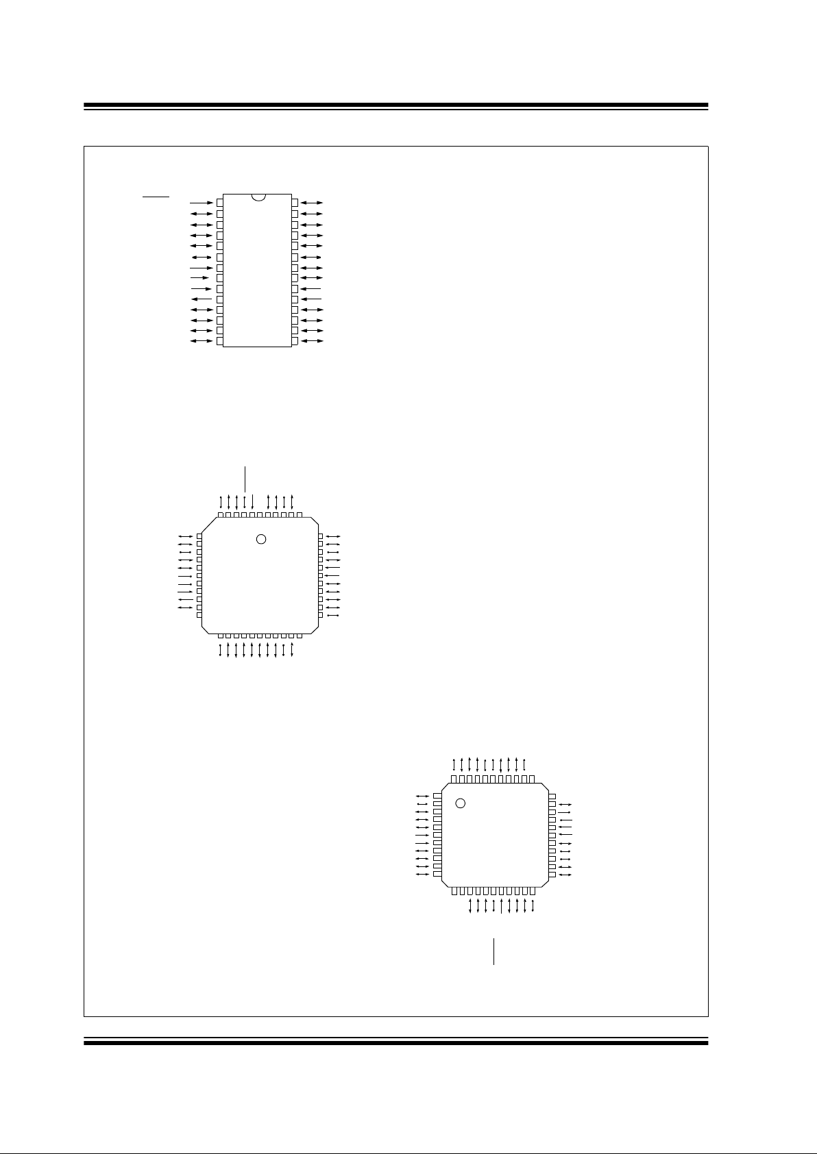
PIC16C77X
DS30275A-page 2 Advance Information 1999 Microchip Technology Inc.
Pin Diagrams
MCLR/VPP
RA0/AN0
RA1/AN1
RA2/AN2/V
REF-/VRL
RA3/AN3/VREF+/VRH
RA4/T0CKI
AV
DD
AVSS
OSC1/CLKIN
OSC2/CLKOUT
RC0/T1OSO/T1CKI
RC1/T1OSI/CCP2
RC2/CCP1
RC3/SCK/SCL
RB7
RB6
RB5
RB4
RB3/AN9/LVDIN
RB2/AN8
RB1/SS
RB0/INT
V
DD
VSS
RC7/RX/DT
RC6/TX/CK
RC5/SDO
RC4/SDI/SDA
• 1
2
3
4
5
6
7
8
9
10
11
12
13
14
28
27
26
25
24
23
22
21
20
19
18
17
16
15
300 mil. SDIP, SOIC, Windowed CERDIP, SSOP
PIC16C773
RB3/AN9/LVDIN
RB2/AN8
RB1/SS
RB0/INT
V
DD
VSS
RD7/PSP7
RD6/PSP6
RD5/PSP5
RD4/PSP4
RC7/RX/DT
RA4/T0CKI
RA5/AN4
RE0/RD/AN5
RE1/WR/AN6
RE2/CS/AN7
AV
DD
AVSS
OSC1/CLKIN
OSC2/CLKOUT
RC0/T1OSO/T1CKI
NC
RA3/AN3/VREF+/VRH
RA2/AN2/V
REF-/VRL
RA1/AN1
RA0/AN0
MCLR
/VPP
NC
RB7
RB6
RB5
RB4
NC
7
8
9
10
11
12
13
14
15
16
17
39
38
37
36
35
34
33
32
31
30
29
NC
RC6/TX/CK
RC5/SDO
RC4/SDI/SDA
RD3/PSP3
RD2/PSP2
RD1/PSP1
RD0/PSP0
RC3/SCK/SCL
RC2/CCP1
65432
1
4443424140
2827262524232221201918
NC
RC0/T1OSO/T1CKI
OSC2/CLKOUT
OSC1/CLKIN
AV
SS
AVDD
RE2/CS/AN7
RE1/WR/AN6
RE0/RD/AN5
RA5/AN4
RA4/T0CKI
RC7/RX/DT
RD4/PSP4
RD5/PSP5
RD6/PSP6
RD7/PSP7
V
SS
VDD
RB0/INT
RB1/SS
RB2/AN8
RB3/AN9/LVDIN
RC6/TX/CK
RC5/SDO
RC4/SDI/SDA
RD3/PSP3
RD2/PSP2
RD1/PSP1
RD0/PSP0
RC3/SCK/SCL
RC2/CCP1
RC1/T1OSI/CCP2
NC
1
2
3
4
5
6
7
8
9
10
11
33
32
31
30
29
28
27
26
25
24
23
RA3/AN3/VREF+/VRH
RA2/AN2/V
REF-/VRL
RA1/AN1
RA0/AN0
MCLR
/VPP
RB7
RB6
RB5
RB4
NC
NC
4443424140393837363534
2221201918171615141312
MQFP
PLCC
TQFP
PIC16C774
PIC16C774
RC1/T1OSI/CCP2

PIC16C77X
1999 Microchip Technology Inc. Advance Information DS30275A-page 3
Key Features
PICmicro™ Mid-Range Reference Manual
(DS33023)
PIC16C773 PIC16C774
Operating Frequency DC - 20 MHz DC - 20 MHz
Resets (and Delays) POR, BOR, MCLR, WDT
(PWRT, OST)
POR, BOR, MCLR, WDT
(PWRT, OST)
Program Memory (14-bit words) 4K 4K
Data Memory (bytes) 256 256
Interrupts 13 14
I/O Ports Ports A,B,C Ports A,B,C,D,E
Timers 3 3
Capture/Compare/PWM modules 2 2
Serial Communications MSSP, USART MSSP, USART
Parallel Communications — PSP
12-bit Analog-to-Digital Module 6 input channels 10 input channels
Instruction Set 35 Instructions 35 Instructions

PIC16C77X
DS30275A-page 4 Advance Information 1999 Microchip Technology Inc.
Table of Contents
1.0 Device Overview............................................................................................................................................................................5
2.0 Memory Organization... ................................................................................................................................................................ 11
3.0 I/O Ports..................... ............... ....................................................... .............. ...................................................................... ........27
4.0 Timer0 Module............................................................................................................................................................................. 39
5.0 Timer1 Module............................................................................................................................................................................. 41
6.0 Timer2 Module............................................................................................................................................................................. 45
7.0 Capture/Compare/PWM (CCP) Module(s)...................................................................................................................................47
8.0 Master Synchronous Serial Port (MSSP) Module........................................................................................................................53
9.0 Addressable Universal Synchronous Asynchronous Receiver Transmitter (USA RT) ................................................................. 97
10.0 Voltage Reference Module and Low-voltage Detect....................................................... .. ....... .. .... .. .. ........................................113
11.0 Analog-to-Digital Converter (A/D) Module ................................................................................................................................. 117
12.0 Special Features of the CPU.....................................................................................................................................................127
13.0 Instruction Set Summary............................................................................................................................................................ 143
14.0 Development Support ................................................................................................................................................................ 145
15.0 Electrical Characteristics............................................................................................................................................................ 151
16.0 DC and AC Characteristics Graphs and Tables ....................................................... .... .... ......... .. .... ..........................................173
17.0 Packaging Infor mation........................... .............. .................................................................................. ............... ............... ...... 175
Appendix A: Revision History......................................................................................................................................................... 187
Appendix B: Device Differences..................................................................................................................................................... 187
Appendix C: Conversion Considerations............................................................ ....... .. .... .. .... .. ....... .. .............................................. 187
Index .................................................................. .. .. .. .... ..... .. .. .. .. .. .. .. .. ..... .... .. .. .. .. .. .. ............................................................................ 189
Bit/Register Cross-Reference List......................................................................................................................................................196
On-Line Support.................................................................... .... .... .. ......... .... .. .... .... ....... .... .................................................................197
Reader Response.............................................................................................................................................................................. 198
PIC16C77X Product Identification System.................................................................................. ....................................................... 199
To Our Valued Customers
Most Current Data Sheet
To obtain the most up-to-date version of this data sheet, please check our Worldwide Web site at:
http://www.microchip.com
You can determine the version of a data sheet by examining its literature number found on the bottom outside corner of any page.
The last character of the literature number is the version number. e.g., DS30000A is version A of document DS30000.
Errata
An errata sheet may exist for current devices, describing minor operational differences (from the data sheet) and recommended
workarounds. As device/documentation issues become known to us, we wil l pub lish an errata sheet. The errata will specify the revision of silicon and revision of document to which it applies.
To deter mine if an errata sheet exists for a particular device, please check with one of the following:
• Microchip’s Worldwide Web site; http://www .mic rochip.com
• Your local Microchip sales office (see last page)
• The Microchip Corporate Literature Center; U.S. FAX: (602) 786-7277
When contacting a sales office or the literature center, please specify which device, revision of silicon and data sheet (include liter-
ature number) you are using.
Corrections to this Data Sheet
We constantly strive to improve the quality of all our products and documentation. We have spent a great deal of time to ensure
that this document is correct. However, we realize that we may hav e missed a few things . If y ou find an y information that is missi n g
or appears in error, please:
• Fill out and mail in the reader response form in the back of this data sheet.
• E-mail us at webmaster@microchip.com.
We appreciate your assistance in making this a better document.

PIC16C77X
1999 Microchip Technology Inc. Advance Information DS30275A-page 5
1.0 DEVICE OVERVIEW
This document contains device-specific information.
Additional information ma y be foun d in the PIC mic ro™
Mid-Range Reference Manual, (DS33023), which may
be obtained from your local Microchip Sales Representative or downloaded from the Microchip website. The
Reference Manual should be considered a complementary document to this data she et, and is high ly recommended reading for a better understanding of the
device architecture and operation of the peripheral
modules.
There a two devices (PIC16C773 and PIC16C774)
covered by this datasheet. The PIC16C773 devices
come in 28-pin packages and the PIC16C774 devices
come in 40-pin packages. The 28-pin devices do not
have a Parallel Slave Port implemented.
The following two figures are device block diagrams
sorted by pin number; 28-pin for Figure 1-1 and 40-pin
for Figure 1-2. The 28-pin and 40-pin pinouts are listed
in T able 1-1 and Table 1-2, respectively.
FIGURE 1-1: PIC16C773 BLOCK DIAGRAM
EPROM
Program
Memory
4K x 14
13
Data Bus
8
14
Program
Bus
Instruction reg
Program Counter
8 Level Stack
(13-bit)
RAM
File
Registers
256 x 8
Direct Addr
7
RAM Addr
(1)
9
Addr MUX
Indirect
Addr
FSR reg
STATUS reg
MUX
ALU
W reg
Power-up
Timer
Oscillator
Start-up Timer
Power-on
Reset
Watchdog
Timer
Instruction
Decode &
Control
OSC1/CLKIN
OSC2/CLKOUT
MCLR
VDD, VSS
PORTA
PORTB
PORTC
RA4/T0CKI
RB0/INT
RB7:RB4
RC0/T1OSO/T1CKI
RC1/T1OSI/CCP2
RC2/CCP1
RC3/SCK/SCL
RC4/SDI/SDA
RC5/SDO
RC6/TX/CK
RC7/RX/DT
8
8
Brown-out
Reset
Note 1: Higher order bits are from the STATUS register.
USART
CCP1,2
Synchronous
Timer0 Timer1 Timer2
Serial Port
RA3/AN3/VREF+/VRH
RA2/AN2/VREF-/VRL
RA1/AN1
RA0/AN0
8
3
Timing
Generation
12-bit
ADC
Precision
Reference
RB1/SS
RB2/AN8
RB3/AN9/LVDIN
Low-voltage
Detect
AVDD
AVSS
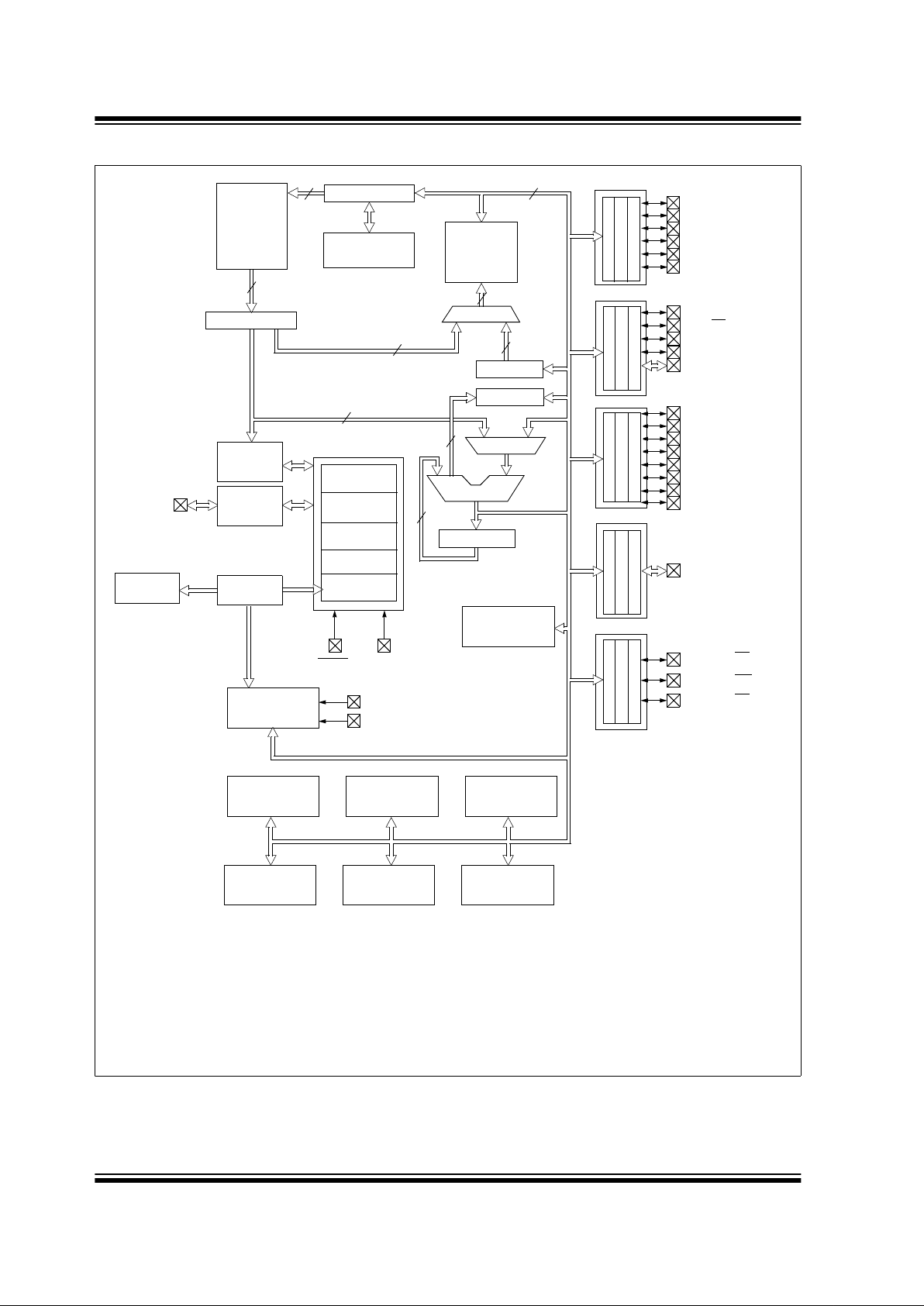
PIC16C77X
DS30275A-page 6 Advance Information 1999 Microchip Technology Inc.
FIGURE 1-2: PIC16C774 BLOCK DIAGRAM
EPROM
Program
Memory
4K x 14
13
Data Bus
8
14
Program
Bus
Instruction reg
Program Counter
8 Leve l Stack
(13-bit)
RAM
File
Registers
256 x 8
Direct Addr
7
RAM Addr
(1)
9
Addr MUX
Indirect
Addr
FSR reg
STATUS reg
MUX
ALU
W reg
Power-up
Timer
Oscillator
Start-up Timer
Power-on
Reset
Watchdog
Timer
Instruction
Decode &
Control
OSC1/CLKIN
OSC2/CLKOUT
MCLR
VDD, VSS
PORTA
PORTB
PORTC
PORTD
PORTE
RA4/T0CKI
RA5/AN4
RB0/INT
RB7:RB4
RC0/T1OSO/T1CKI
RC1/T1OSI/CCP2
RC2/CCP1
RC3/SCK/SCL
RC4/SDI/SDA
RC5/SDO
RC6/TX/CK
RC7/RX/DT
RD7/PSP7:RD0/PSP0
RE0/AN5/RD
RE1/AN6/WR
RE2/AN7/CS
8
8
Brown-out
Reset
Note 1: Higher order bits are from the STATUS register.
USART
CCP1,2
Synchronous
Timer0 Timer1 Timer2
Serial Port
RA3/AN3/VREF+/VRH
RA2/AN2/VREF-/VRL
RA1/AN1
RA0/AN0
Parallel Slave Port
8
3
Timing
Generation
12-bit
ADC
Precision
Reference
RB1/SS
RB2/AN8
RB3/AN9/LVDIN
Low-voltage
Detect
AVDD
AVSS

PIC16C77X
1999 Microchip Technology Inc. Advance Information DS30275A-page 7
T ABLE 1-1 PIC16C773 PINOUT DESCRIPTION
Pin Name
DIP,
SSOP,
SOIC
Pin#
I/O/P
Type
Buffer
Type
Description
OSC1/CLKIN 9 I
ST/CMOS
(3)
Oscillator crystal input/external clock source input.
OSC2/CLKOUT 10 O — Oscillator crystal output. Connects to crystal or resonator in crystal
oscillator mode. In RC mode, the OSC2 pin outputs CLKOUT which has
1/4 the frequency of OSC1, and denotes the instruction cycle rate.
MCLR
/VPP
1 I/P ST Master clear (reset) input or programming voltage input. This pin is an
active low reset to the device.
PORTA is a bi-directional I/O port.
RA0/AN0 2 I/O TTL RA0 can also be analog input0
RA1/AN1 3 I/O TTL RA1 can also be analog input1
RA2/AN2/V
REF-/VRL 4 I/O TTL RA2 can also be analog input2 or negative analog reference voltage
input or internal voltage reference low
RA3/AN3/V
REF+/VRH 5 I/O TTL RA3 can also be analog input3 or positiv e analog reference v oltage
input or internal voltage reference high
RA4/T0CKI 6 I/O ST RA4 can also be the clock input to the Timer0 module. Output is
open drain type.
PORTB is a bi-directional I/O port. PORTB can be software pro-
grammed for internal weak pull-up on all inputs.
RB0/INT 21 I/O TTL/ST
(1)
RB0 can also be the external interrupt pin.
RB1/SS
22 I/O TTL/ST
(1)
RB1 can also be the SSP slave select
RB2/AN8 23 I/O TTL RB2 can also be analog input8
RB3/AN9/LVDIN 24 I/O TTL RB3 can also be analog input9 or the low voltage detect input
reference
RB4 25 I/O TTL Interrupt on change pin.
RB5 26 I/O TTL Interrupt on change pin.
RB6 27 I/O TTL/ST
(2)
Interrupt on change pin. Serial programming clock.
RB7 28 I/O TTL/ST
(2)
Interrupt on change pin. Serial programming data.
PORTC is a bi-directional I/O port.
RC0/T1OSO/T1CKI 11 I/O ST RC0 can also be the Timer1 oscillator output or Timer1 clock input.
RC1/T1OSI/CCP2 12 I/O ST RC1 can also be the Timer1 oscillator input or Capture2 input/
Compare2 output/PWM2 output.
RC2/CCP1 13 I/O ST RC2 can also be the Capture1 input/Compare1 output/PWM1
output.
RC3/SCK/SCL 14 I/O ST RC3 can also be the synchronous serial clock input/output for both
SPI and I
2
C modes.
RC4/SDI/SDA 15 I/O ST RC4 can also be the SPI Data In (SPI mode) or
data I/O (I
2
C mode).
RC5/SDO 16 I/O ST RC5 can also be the SPI Data Out (SPI mode).
RC6/TX/CK 17 I/O ST RC6 can also be the USART Asynchronous Transmit or
Synchronous Clock.
RC7/RX/DT 18 I/O ST RC7 can also be the USART Asynchronous Receive or
Synchronous Data.
AV
SS 8 P Ground reference for A/D converter
AV
DD 7 P Positive supply for A/D converter
V
SS 19 P — Ground reference for logic and I/O pins.
V
DD 20 P — Positive supply for logic and I/O pins.
Legend: I = input O = output I/O = input/output P = power
— = Not used TTL = TTL input ST = Schmitt Trigger input
Note 1: This buffer is a Schmitt Trigger input when configured for the multiplexed function.
2: This buffer is a Schmitt Trigger input when used in serial programming mode.
3: This buffer is a Schmitt Trigger input when configured in RC oscillator mode and a CMOS input otherwise.

PIC16C77X
DS30275A-page 8 Advance Information 1999 Microchip Technology Inc.
TABLE 1-2 PIC16C774 PINOUT DESCRIPTION
Pin Name
DIP
Pin#
PLCC
Pin#
QFP
Pin#
I/O/P
Type
Buffer
Type
Description
OSC1/CLKIN 13 14 30 I ST/CMOS
(4)
Oscillator crystal input/external clock source input.
OSC2/CLKOUT 14 15 31 O — Oscillator crystal output. Connects to crystal or resonator
in crystal oscillator mode. In RC mode, OSC2 pin outputs
CLKOUT which has 1/4 the frequency of OSC1, and
denotes the instruction cycle rate.
MCLR
/VPP 1 2 18 I/P ST Master clear (reset) input or programming voltage input.
This pin is an active low reset to the device.
PORTA is a bi-directional I/O por t.
RA0/AN0 2 3 19 I/O TTL RA0 can also be analog input0
RA1/AN1 3 4 20 I/O TTL RA1 can also be analog input1
RA2/AN2/V
REF-/VRL 4 5 2 1 I/O TTL
RA2 can also be analog input2 or negative analog
reference voltage input or internal voltage reference
low
RA3/AN3/V
REF+/VRH 5 6 22 I/O TTL
RA3 can also be analog input3 or positive analog
reference voltage input or internal voltage reference
high
RA4/T0CKI 6 7 23 I/O ST RA4 can also be the clock input to the Timer0 timer/
counter. Output is open drain type.
RA5/AN4 7 8 24 I/O TTL RA5 can also be analog input4
PORTB is a bi-directional I/O port. PORTB can be soft-
ware programmed for internal weak pull-up on all inputs.
RB0/INT 33 36 8 I/O TTL/ST
(1)
RB0 can also be the external interrupt pin.
RB1/SS
34 37 9 I/O TTL/ST
(1)
RB1 can also be the SSP slave select
RB2/AN8 35 38 10 I/O TTL RB2 can also be analog input8
RB3/AN9/LVDIN 36 39 11 I/O TTL RB3 can also be analog input9 or input reference for
low voltage detect
RB4 37 41 14 I/O TTL Interrupt on change pin.
RB5 38 42 15 I/O TTL Interrupt on change pin.
RB6 39 43 16 I/O TTL/ST
(2)
Interrupt on change pin. Serial programming clock.
RB7 40 44 17 I/O TTL/ST
(2)
Interrupt on change pin. Serial programming data.
Legend: I = input O = output I/O = input/output P = power
— = Not used TTL = TTL input ST = Schmitt Trigger input
Note 1: This buffer is a Schmitt Trigger input when configured for the multiplexed function.
2: This buffer is a Schmitt Trigger input when used in serial programming mode.
3: This buffer is a Schmitt Trigger input when configured as general purpose I/O and a TTL input when used in the Parallel
Slave Port mode (for interfacing to a microprocessor bus).
4: This buffer is a Schmitt Trigger input when configured in RC oscillator mode and a CMOS input otherwise.

PIC16C77X
1999 Microchip Technology Inc. Advance Information DS30275A-page 9
PORTC is a bi-directional I/O port.
RC0/T1OSO/T1CKI 15 16 32 I/O ST RC0 can also be the Timer1 oscillator output or a
Timer1 clock input.
RC1/T1OSI/CCP2
16 18 35 I/O ST RC1 can also be the Timer1 oscillator input or
Capture2 input/Compare2 output/PWM2 output.
RC2/CCP1
17 19 36 I/O ST RC2 can also be the Capture1 input/Compare1
output/PWM1 output.
RC3/SCK/SCL
18 20 37 I/O ST RC3 can also be the synchronous serial clock input/
output for both SPI and I
2
C modes.
RC4/SDI/SDA
23 25 42 I/O ST RC4 can also be the SPI Data In (SPI mode) or
data I/O (I
2
C mode).
RC5/SDO
24 26 43 I/O ST RC5 can also be the SPI Data Out
(SPI mode).
RC6/TX/CK
25 27 44 I/O ST RC6 can also be the USART Asynchronous
Transmit or Synchronous Clock.
RC7/RX/DT
26 29 1 I/O ST RC7 can also be the USART Asynchronous Receive
or Synchronous Data.
PORTD is a bi-directional I/O port or parallel slave port
when interfacing to a microprocessor bus.
RD0/PSP0 19 21 38 I/O ST/TTL
(3)
RD1/PSP1 20 22 39 I/O ST/TTL
(3)
RD2/PSP2 21 23 40 I/O ST/TTL
(3)
RD3/PSP3 22 24 41 I/O ST/TTL
(3)
RD4/PSP4 27 30 2 I/O ST/TTL
(3)
RD5/PSP5 28 31 3 I/O ST/TTL
(3)
RD6/PSP6 29 32 4 I/O ST/TTL
(3)
RD7/PSP7 30 33 5 I/O ST/TTL
(3)
PORTE is a bi-directional I/O port.
RE0/RD
/AN5 8 9 25 I/O ST/TTL
(3)
RE0 can also be read control for the parallel slave
port, or analog input5.
RE1/WR
/AN6 9 10 26 I/O ST/TTL
(3)
RE1 can also be write control for the parallel slave
port, or analog input6.
RE2/CS
/AN7 10 11 27 I/O ST/TTL
(3)
RE2 can also be select control for the parallel slave
port, or analog input7.
AVss 12 13 29 P
Ground reference for A/D converter
AV
DD 11 12 28 P
Positive supply for A/D converter
V
SS 31 34 6 P — Ground reference for logic and I/O pins.
V
DD 32 35 7 P — Positive supply for logic and I/O pins.
NC — 1,17,28,4012,13,
33,34
— These pins are not internally connected. These pins
should be left unconnected.
T ABLE 1-2 PIC16C774 PINOUT DESCRIPTION (Cont.’d)
Pin Name
DIP
Pin#
PLCC
Pin#
QFP
Pin#
I/O/P
Type
Buffer
Type
Description
Legend: I = input O = output I/O = input/output P = power
— = Not used TTL = TTL input ST = Schmitt Trigger input
Note 1: This buffer is a Schmitt Trigger input when configured for the multiplexed function.
2: This buffer is a Schmitt Trigger input when used in serial programming mode.
3: This buffer is a Schmitt Trigger input when configured as general purpose I/O and a TTL input when used in the Parallel
Slave Port mode (for interfacing to a microprocessor bus).
4: This buffer is a Schmitt Trigger input when configured in RC oscillator mode and a CMOS input otherwise.

PIC16C77X
DS30275A-page 10 Advance Information 1999 Microchip Technology Inc.
NOTES:
PIC16C77X
1999 Microchip Technology Inc. Advance Information DS30275A-page 11
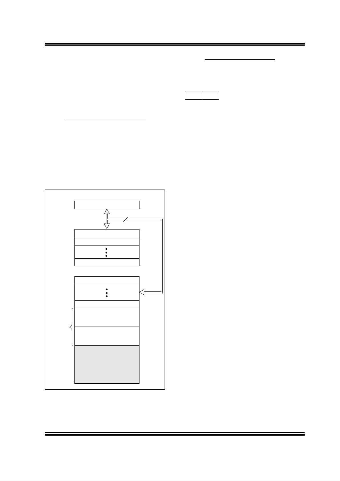
2.0 MEMORY ORGANIZATION
There are two memory blocks in each of these
PICmicro
®
microcontrollers. Each block (Program Memory and Data Memory) has its own bus
so that concurrent access can occur.
Additional information on devi ce memo ry may be foun d
in the PICmicro Mid-Range Reference Manual,
(DS33023).
2.1 Program Memory Organization
The PIC16C77X PICmicros have a 13-bit program
counter capable of addressing an 8K x 14 program
memory space. Each de vice has 4K x 14 w ords of pr ogram memory. Accessing a location above the physically implemented address will cause a wraparound.
The reset vector is at 0000h and the interrupt vector is
at 0004h.
FIGURE 2-1: PROGRAM MEMORY MAP
AND STACK
2.2 Data Memory Organization
The data memory is partitioned into multiple banks
which contain the General Purpose Registers and the
Special Function Registers. Bits RP1 and RP0 are the
bank select bits.
= 00 → Bank0
= 01 → Bank1
= 10 → Bank2
= 11 → Bank3
Each bank extends up to 7Fh (128 bytes). The lower
locations of each bank are reserved for the Special
Function Registers . Abo v e the Spec ial Fun ction Re gisters are General Purpose Registers, implemented as
static RAM. All implemented banks contain special
function registers. Some “high use” special function
registers from one bank may be mirrored in another
bank for code reduction and quicker access.
2.2.1 GENERAL PURPOSE REGISTER FILE
The register file can be a ccessed ei ther direc tly, or indi-
rectly through the File Select Register FSR.
PC<12:0>
13
0000h
0004h
0005h
Stack Level 1
Stack Level 8
Reset Vector
Interrupt Vector
On-chip
CALL, RETURN
RETFIE, RETLW
Stack Level 2
Program
Memory
Page 0
Page 1
07FFh
0800h
0FFFh
1000h
3FFFh
RP1 RP0 (STATUS<6:5>)

PIC16C77X
DS30275A-page 12 Advance Information 1999 Microchip Technology Inc.
FIGURE 2-2: REGISTER FILE MAP
Indirect addr.
(*)
TMR0
PCL
STATUS
FSR
PORTA
PORTB
PORTC
PCLATH
INTCON
PIR1
TMR1L
TMR1H
T1CON
TMR2
T2CON
SSPBUF
SSPCON
CCPR1L
CCPR1H
CCP1CON
OPTION_REG
PCL
STATUS
FSR
TRISA
TRISB
TRISC
PCLATH
INTCON
PIE1
PCON
PR2
SSPADD
SSPSTAT
00h
01h
02h
03h
04h
05h
06h
07h
08h
09h
0Ah
0Bh
0Ch
0Dh
0Eh
0Fh
10h
11h
12h
13h
14h
15h
16h
17h
18h
19h
1Ah
1Bh
1Ch
1Dh
1Eh
1Fh
80h
81h
82h
83h
84h
85h
86h
87h
88h
89h
8Ah
8Bh
8Ch
8Dh
8Eh
8Fh
90h
91h
92h
93h
94h
95h
96h
97h
98h
99h
9Ah
9Bh
9Ch
9Dh
9Eh
9Fh
20h
A0h
7Fh
FFh
Bank 0 Bank 1
Unimplemented data memory locations, read as ’0’.
* Not a physical register.
Indirect addr.
(*)
PORTD
PORTE
TRISD
ADRESL
TRISE
PIR2
PIE2
RCSTA
TXREG
RCREG
CCPR2L
CCPR2H
CCP2CON
ADRESH
ADCON0
TXSTA
SPBRG
ADCON1
General
Purpose
Register
General
Purpose
Register
EFh
F0h
accesses
70h-7Fh
96 Bytes
80 Bytes
(1)
(1)
(1)
(1)
(1) Not implemented on PIC16C773.
LVDCON
100h
101h
102h
103h
104h
105h
106h
107h
108h
109h
10Ah
10Bh
10Ch
10Dh
10Eh
10Fh
110h
111h
112h
113h
114h
115h
116h
117h
118h
119h
11Ah
11Bh
11Ch
11Dh
11Eh
11Fh
120h
17Fh
Bank 2
6Fh
70h
File
Address
PCL
STATUS
FSR
PCLATH
INTCON
180h
181h
182h
183h
184h
185h
186h
187h
188h
189h
18Ah
18Bh
18Ch
18Dh
18Eh
18Fh
190h
191h
192h
193h
194h
195h
196h
197h
198h
199h
19Ah
19Bh
19Ch
19Dh
19Eh
19Fh
1A0h
1FFh
Bank 3
Indirect addr.
(*)
OPTION_REG
1EFh
1F0h
accesses
70h - 7Fh
TRISB
PCL
STATUS
FSR
PCLATH
INTCON
Indirect addr.
(*)
TMR0
General
Purpose
Register
accesses
70h - 7Fh
PORTB
80 Bytes
File
Address
File
Address
File
Address
REFCON
SSPCON2
PIC16C77X
1999 Microchip Technology Inc. Advance Information DS30275A-page 13
2.2.2 SPECIAL FUNCTION REGISTERS
The Special Function Registers are registers used by
the CPU and Peripheral Modules for controlling the
desired operation of the device. These registers are
implemented as static RAM. A list of these registers is
given in Table 2-1.
The special fu nction re gisters can be classifi ed into two
sets; core (CPU) and periphe ral. Those registers associated with the core functions are described in detail in
this section. Those related to the operation of the
peripheral features are described in detail in that
peripheral feature section.
TABLE 2-1 PIC16C77X SPECIAL FUNCTION REGISTER SUMMARY
Address Name Bit 7 Bit 6 Bit 5 Bit 4 Bit 3 Bit 2 Bit 1 Bit 0
Value on:
POR,
BOR
Value on all
other resets
(2)
Bank 0
00h
(4)
INDF Addressing this location uses contents of FSR to address data memory (not a physical register) 0000 0000 0000 0000
01h TMR0 Timer0 module’s register xxxx xxxx uuuu uuuu
02h
(4)
PCL Program Counter's (PC) Least Significant Byte 0000 0000 0000 0000
03h
(4)
ST ATUS IRP RP1 RP0 TO PD ZDCC0001 1xxx 000q quuu
04h
(4)
FSR Indirect data memory address pointer xxxx xxxx uuuu uuuu
05h PORTA
— —PORTA5
(5)
PORTA Data Latch when written: PORTA<4:0> pins when read --0x 0000 --0u 0000
06h PORTB PORTB Data Latch when written: PORTB pins when read xxxx 11xx uuuu 11uu
07h PORTC PORTC Data Latch when written: PORTC pins when read xxxx xxxx uuuu uuuu
08h
(5)
PORTD PORTD Data Latch when written: PORTD pins when read xxxx xxxx uuuu uuuu
09h
(5)
PORTE — — — — — RE2 RE1 RE0 ---- -000 ---- -000
0Ah
(1,4)
PCLATH — — — Write Buffer for the upper 5 bits of the Program Counter ---0 0000 ---0 0000
0Bh
(4)
INTCON GIE PEIE T0IE INTE RBIE T0IF INTF RBIF 0000 000x 0000 000u
0Ch PIR1 PSPIF
(3)
ADIF RCIF TXIF SSPIF CCP1IF TMR2IF TMR1IF 0000 0000 0000 0000
0Dh PIR2 LVDIF
— — –BCLIF— — CCP2 IF 0--- 0--0 0--- 0--0
0Eh TMR1L Holding register for the Least Significant Byte of the 16-bit TMR1 register xxxx xxxx uuuu uuuu
0Fh TMR1H Holding register for the Most Significant Byte of the 16-bit TMR1 register xxxx xxxx uuuu uuuu
10h T1CON
— — T1CKPS1 T1CKPS0 T1OSCEN T1SYNC TMR1CS TMR1ON - -00 0000 --uu uuuu
11h TMR2 Timer2 module’s register 0000 0000 0000 0000
12h T2CON
— TOUTPS3 TOUTPS2 TOUTPS1 TOUTPS0 TMR2ON T2CKPS1 T2CKPS0 -000 0000 -000 0000
13h SSPBUF Synchronous Serial Port Receive Buffer/Transmit Register xxxx xxxx uuuu uuuu
14h SSPCON WCOL SSPOV SSPEN CKP SSPM3 SSPM2 SSPM1 SSPM0 0000 0000 000 0 0000
15h CCPR1L Capture/Compare/PWM Register1 (LSB) xxxx xxxx uuuu uuuu
16h CCPR1H Capture/Compare/PWM Register1 (MSB) xxxx xxxx uuuu uuuu
17h CCP1CON
— — CCP1X CCP1Y CCP1M3 CCP1M2 CCP1M1 CCP1M0 --00 0000 --00 0000
18h RCSTA SPEN RX9 SREN CREN ADDEN FERR OERR RX9D 0000 000x 0000 000x
19h TXREG USART Transmit Data Register 0000 0000 0000 0000
1Ah RCREG USART Receive Data Register 0000 0000 0000 0000
1Bh CCPR2L Capture/Compare/PWM Register2 (LSB) xxxx xxxx uuuu uuuu
1Ch CCPR2H Capture/Compare/PWM Register2 (MSB) xxxx xxxx uuuu uuuu
1Dh CCP2CON
— — CCP2X CCP2Y CCP2M3 CCP2M2 CCP2M1 CCP2M0 --00 0000 --00 0000
1Eh ADRESH A/D High Byte Result Register xxxx xxxx uuuu uuuu
1Fh ADCON0 ADCS1 ADCS0 CHS2 CHS1 CHS0 GO/DONE
CHS3 ADON 0000 0000 0000 0000
Legend: x = unknown, u = unchanged, q = value depends on condition, - = unimplemented read as '0'.
Shaded locations are unimplemented, read as ‘0’.
Note 1: The upper byte of the program counter is not directly accessible. PCLATH is a holding register for the PC<12:8> whose contents are transferred to
the upper byte of the program counter.
2: Other (non power-up) resets include external reset through MCLR
and Watchdog Timer Reset.
3: Bits PSPIE and PSPIF are reserved on the 28-pin devices, always maintain these bits clear.
4: These registers can be addressed from any bank.
5: These registers/bits are not implemented on the 28-pin devices read as '0'.
PIC16C77X
DS30275A-page 14 Advance Information 1999 Microchip Technology Inc.
Bank 1
80h
(4)
INDF Addressing this location uses contents of FSR to address data memory (not a physical register) 0000 0000 0000 0000
81h OPTION_REG RBPU
INTEDG T0CS T0SE PSA PS2 PS1 PS0 1111 1111 1111 1111
82h
(4)
PCL Program Counter’s (PC) Least Significant Byte 0000 0000 0000 0000
83h
(4)
ST ATUS IRP RP1 RP0 TO PD ZDCC0001 1xxx 000q quuu
84h
(4)
FSR Indirect data memory address pointer xxxx xxxx uuuu uuuu
85h TRISA
— —bit5
(5)
PORTA Data Direction Register --11 1111 --11 1111
86h TRISB PORTB Data Direction Register 1111 1111 1111 1111
87h TRISC PORTC Data Direction Register 1111 1111 1111 1111
88h
(5)
TRISD PORTD Data Direction Register 1111 1111 1111 1111
89h
(5)
TRISE IBF OBF IBOV PSPMODE — PORTE Data Direction Bits 0000 -111 0000 -111
8Ah
(1,4)
PCLATH — — — Write Buffer for the upper 5 bits of the Program Counter ---0 0000 ---0 0000
8Bh
(4)
INTCON GIE PEIE T0IE INTE RBIE T0IF INTF RBIF 0000 000x 0000 000u
8Ch PIE1 PSPIE
(3)
ADIE RCIE TXIE SSPIE CCP1IE TMR2IE TMR1IE 0000 0000 0000 0000
8Dh PIE2 LVDIE
— — —BCLIE— — CCP2IE 0--- 0--0 0--- 0--0
8Eh PCON
— — — — — —PORBOR ---- --qq ---- --uu
8Fh — Unimplemented — —
90h — Unimplemented — —
91h SSPCON2 GCEN AKSTAT AKDT AKEN RCEN PEN RSEN SEN 0000 0000 0000 0000
92h PR2 Timer2 Period Register 1111 1111 1111 1111
93h SSPADD Sy nchr on ous Ser i al Por t (I
2
C mode) Address Register 0000 0000 0000 0000
94h SSPSTAT SMP CKE D/A
PSR/WUA BF 0000 0000 0000 0000
95h — Unimplemented — —
96h — Unimplemented — —
97h — Unimplemented — —
98h TXSTA CSRC TX9 TXEN SYNC
— BRGH TRMT TX9D 0000 -010 0000 -010
99h SPBRG Baud Rate Generator Register 0000 0000 0000 0000
9Ah — Unimplemented — —
9Bh REFCON VRHEN VRLEN VRHOEN VRLOEN
— — — — 0000 ---- 0000 ----
9Ch LVDCON
— — BGST LVDEN LV3 LV2 LV1 LV0 --00 0101 --00 0101
9Ah — Unimplemented — —
9Eh ADRESL A/D Low Byte Result Register xxxx xxxx uuuu uuuu
9Fh ADCON1 ADFM VCFG2 VCFG1 VCFG0 PCFG3 PCFG2 PCFG1 PCFG0 0000 0000 0000 0000
TABLE 2-1 PIC16C77X SPECIAL FUNCTION REGISTER SUMMARY (Cont.’d)
Address Name Bit 7 Bit 6 Bit 5 Bit 4 Bit 3 Bit 2 Bit 1 Bit 0
Value on:
POR,
BOR
Value on all
other resets
(2)
Legend: x = unknown, u = unchanged, q = value depends on condition, - = unimplemented read as ’0’.
Shaded locations are unimplemented, read as ‘0’.
Note 1: The upper byte of the program counter is not directly accessible. PCLA TH is a holding register for the PC<12:8> whose contents are transferred to
the upper byte of the program counter.
2: Other (non power-up) resets include external reset through MCLR
and Watchdog Timer Reset.
3: Bits PSPIE and PSPIF are reserved on the 28-pin devices, always maintain these bits clear.
4: These registers can be addressed from any bank.
5: These registers/bits are not implemented on the 28-pin devices read as '0'.
PIC16C77X
1999 Microchip Technology Inc. Advance Information DS30275A-page 15
Bank 2
100h
(4)
INDF Addressing this location uses contents of FSR to address data memory (not a physical register) 0000 0000 0000 0000
101h TMR0 Timer0 module’s register xxxx xxxx uuuu uuuu
102h
(4)
PCL Program Counter's (PC) Least Significant Byte 0000 0000 0000 0000
103h
(4)
STATUS I RP RP1 RP0 TO PD ZDCC0001 1xxx 000q quuu
104h
(4)
FSR Indirect data memory address pointer xxxx xxxx uuuu uuuu
105h — Unimplemented — —
106h PORTB PORTB Data Latch when written: PORTB pins when read xxxx 11xx uuuu 11uu
107h — Unimplemented — —
108h — Unimplemented — —
109h — Unimplemented — —
10Ah
(1,4)
PCLATH — — — Write Buffer for the upper 5 bits of the Program Counter ---0 0000 ---0 0000
10Bh
(4)
INTCON GIE PEIE T0IE INTE RBIE T0IF INTF RBIF 0000 000x 0000 000u
10Ch10Fh
— Unimplemented — —
Bank 3
180h
(4)
INDF Addressing this location uses contents of FSR to address data memory (not a physical register) 0000 0000 0000 0000
181h O PTION_REG RBPU
INTEDG T0CS T0SE PSA PS2 PS1 PS0 1111 1111 1111 1111
182h
(4)
PCL Program Counter's (PC) Least Significant Byte 0000 0000 0000 0000
183h
(4)
STATUS I RP RP1 RP0 TO PD ZDCC0001 1xxx 000q quuu
184h
(4)
FSR Indirect data memory address pointer xxxx xxxx uuuu uuuu
185h — Unimplemented — —
186h TRISB PORTB Data Direction Register 1111 1111 1111 1111
187h — Unimplemented — —
188h — Unimplemented — —
189h — Unimplemented — —
18Ah
(1,4)
PCLATH — — —
Write Buffer for the upper 5 bits of the Program Counter
---0 0000 ---0 0000
18Bh
(4)
INTCON GIE PEIE T0IE INTE RBIE T0IF INTF RBIF 0000 000x 0000 000u
18Ch-
18Fh
— Unimplemented — —
TABLE 2-1 PIC16C77X SPECIAL FUNCTION REGISTER SUMMARY (Cont.’d)
Address Name Bit 7 Bit 6 Bit 5 Bit 4 Bit 3 Bit 2 Bit 1 Bit 0
Value on:
POR,
BOR
Value on all
other resets
(2)
Legend: x = unknown, u = unchanged, q = value depends on condition, - = unimplemented read as ’0’.
Shaded locations are unimplemented, read as ‘0’.
Note 1: The upper byte of the program counter is not directly accessible. PCLATH is a holding register for the PC<12:8> whose contents are transferred to
the upper byte of the program counter.
2: Other (non power-up) resets include external reset through MCLR
and Watchdog Timer Reset.
3: Bits PSPIE and PSPIF are reserved on the 28-pin devices, always maintain these bits clear.
4: These registers can be addressed from any bank.
5: These registers/bits are not implemented on the 28-pin devices read as '0'.

PIC16C77X
DS30275A-page 16 Advance Information 1999 Microchip Technology Inc.
2.2.2.1 STATUS REGISTER
The STATUS register, shown in Figure 2-3, contains
the arithmetic status of th e ALU , the RE SET status an d
the bank select bits for data memory.
The STATUS register can be the destination for any
instruction, as with any other register. If the STATUS
register is the destination for an instruction that affects
the Z, DC or C bits, then the write to these three bits is
disabled. The se bi ts ar e set or c leared a ccordi ng to the
device logic. Fur th erm ore, the TO
and PD bits are not
writable. Therefore, the result of an instruction with the
STATUS register as destination may be different than
intended.
For example, CLRF STATUS will clear th e up p er- th r ee
bits and set the Z bi t. T his l ea v es the STATUS register
as 000u u1uu (where u = unchanged).
It is recommended, therefore, that only BCF, BSF,
SWAPF and MOVWF instructions are used to alter t he
STATUS register because these instructions do not
affect the Z, C o r DC bits from th e STATUS register. F or
other instructions, not affecting any status bit s , s ee th e
"Instruction Set Summary."
FIGURE 2-3: STATUS REGISTER (ADDRESS 03h, 83h, 103h, 183h)
Note 1: The C and DC bits oper ate as a borro w and
digit borrow
bit, respectively , in subtraction.
See the SUBLW and SUBWF instructions for
examples.
R/W-0 R/W-0 R/W-0 R-1 R-1 R/W-x R/W-x R/W-x
IRP RP1 RP0 TO
PD Z DC C R = Readable bit
W = Writable bit
U = Unimplemented bit,
read as ‘0’
- n = Value at POR reset
bit7 bit0
bit 7: IRP: Register Bank Select bit (used for indirect addressing)
1 = Bank 2, 3 (100h - 1FFh)
0 = Bank 0, 1 (00h - FFh)
bit 6-5: RP1:RP0: Register Bank Select bits (used for direct addressing)
11 = Bank 3 (180h - 1FFh)
10 = Bank 2 (100h - 17Fh)
01 = Bank 1 (80h - FFh)
00 = Bank 0 (00h - 7Fh)
Each bank is 128 bytes
bit 4: TO
: Time-out bit
1 = After power-up, CLRWDT instruction, or SLEEP instructi on
0 = A WDT time-out occurred
bit 3: PD
: Power-down bit
1 = After power-up or by the CLRWDT instruction
0 = By execution of th e SLEEP instruction
bit 2: Z: Zero b i t
1 = The result of an arithmetic or logic operation is zero
0 = The result of an arithmetic or logic operation is not zero
bit 1: DC: Digit carry/borrow
bit (ADDWF, ADDLW,SUBLW,SUBWF instructions) (for borrow the polari ty i s reversed)
1 = A carry-out from the 4th low order bit of the result occurred
0 = No carry-out from the 4th low order bit of the result
bit 0: C: Carry/borrow
bit (ADDWF, ADDLW,SUBLW,SUBWF instructions)
1 = A carry-out from the most significant bit of the result occurred
0 = No carry-out from the most significant bit of the result occurred
Note: For borrow
the polarity is reversed. A subtraction is executed by adding the two’s complement of the
second operand. For rotate (RRF, RLF) instructions, this bit is loaded with either the high or low order bit of
the source register.
PIC16C77X
1999 Microchip Technology Inc. Advance Information DS30275A-page 17
2.2.2.2 OPTION_REG REGISTER
The OPTION_REG register is a readable and writable
register which contai ns v arious control bits to conf igure
the TMR0 prescaler/WDT postscaler (single assignable regist er kno wn also as the prescale r), the Ext ernal
INT Interrupt, TMR0, and the weak pull-up s on PORTB.
FIGURE 2-4: OPTION_REG REGISTER (ADDRESS 81h, 181h)
Note: To achieve a 1:1 prescaler assignment for
the TMR0 register, assign the prescaler to
the Watchdog Timer.
R/W-1 R/W-1 R/W-1 R/W-1 R/W-1 R/W-1 R/W-1 R/W-1
RBPU
INTEDG T0CS T0SE PSA PS2 PS1 PS0 R = Readable bit
W = Writable bit
U = Unimplemented bit,
read as ‘0’
- n = Value at POR reset
bit7 bit0
bit 7: RBPU: PORTB Pull-up Enable bit
1 = PORTB pull-ups are disabled
0 = PORTB pull-ups are enab led b y ind iv idu al port latch va lue s
bit 6: INTEDG: Interrupt Edge Select bit
1 = Interrupt on rising edge of RB0/INT pin
0 = Interrupt on falling edge of RB0/INT pin
bit 5: T0CS: TMR0 Clock Source Select bit
1 = Transition on RA4/T0CKI pin
0 = Internal instruction cycle clock (CLKOUT)
bit 4: T0SE: TMR0 Source Edge Select bit
1 = Increment on high-to-low transition on RA4/T0CKI pin
0 = Increment on low-to-high transition on RA4/T0CKI pin
bit 3: PSA: Prescaler Assignment bit
1 = Prescaler is assigned to the WDT
0 = Prescaler is assigned to the Timer0 module
bit 2-0: PS2:PS0: Prescaler Rate Select bits
000
001
010
011
100
101
110
111
1 : 2
1 : 4
1 : 8
1 : 16
1 : 32
1 : 64
1 : 128
1 : 256
1 : 1
1 : 2
1 : 4
1 : 8
1 : 16
1 : 32
1 : 64
1 : 128
Bit Value TMR0 Rate WDT Rate

PIC16C77X
DS30275A-page 18 Advance Information 1999 Microchip Technology Inc.
2.2.2.3 INTCON REGISTER
The INTCON Regi ster i s a rea dab le a nd w ritabl e regi s-
ter which contains various enable and flag bits for the
TMR0 register overflow, RB Port change and External
RB0/INT pin interrupts.
FIGURE 2-5: INTCON REGISTER (ADDRESS 0Bh, 8Bh, 10Bh, 18Bh)
Note: Interrupt flag bits get set when an interrupt
condition occurs regardless of the state of
its corresponding enable bit or the global
enable bit, GIE (INTCON<7>). User software should ensure the appropriate interrupt flag bits are clear prior to enabling an
interrupt.
R/W-0 R/W-0 R/W-0 R/W-0 R/W-0 R/W-0 R/W-0 R/W-x
GIE PEIE T0IE INTE RBIE T0IF INTF RBIF R = Readable bit
W = Writable bit
U = Unimplemented bit,
read as ‘0’
- n = Value at POR reset
bit7 bit0
bit 7: GIE: Global Interrupt Enable bit
1 = Enables all un-masked interrupts
0 = Disables all interrupts
bit 6: PEIE: Peripheral Interrupt Enable bit
1 = Enables all un-masked peripheral interrupts
0 = Disables all peripheral interrupts
bit 5: T0IE: TMR0 Overflow Interrupt Enable bit
1 = Enables the TMR0 interrupt
0 = Disables the TMR0 interrupt
bit 4: IINTE: RB0/INT External Interrupt Enable bit
1 = Enables the RB0/INT external interrupt
0 = Disables the RB0/INT external interrupt
bit 3: RBIE: RB Port Change Interrupt Enable bit
1 = Enables the RB port change interrupt
0 = Disables the RB port change interrupt
bit 2: T0IF: TMR0 Overflow Interrupt Flag bit
1 = TMR0 regi ster has overflowed (mus t be cleared i n software)
0 = TMR0 register did not overflow
bit 1: INTF: RB0/INT External Interrupt Flag bit
1 = The RB0/INT external interrupt occurred (must be cleared in software)
0 = The RB0/INT external interrupt did not occur
bit 0: RBIF: RB Port Change Interrupt Flag bit
1 = At least one of the RB7:RB4 pins changed state (must be cleared in software)
0 = None of the RB7:RB4 pins have changed state

PIC16C77X
1999 Microchip Technology Inc. Advance Information DS30275A-page 19
2.2.2.4 PIE1 R EGISTER
This register contains the individual enable bits for the
peripheral interrupts.
FIGURE 2-6: PIE1 REGISTER (ADDRESS 8Ch)
Note: Bit PEIE (INTCON<6>) must be set to
enable any peripheral interrupt.
R/W-0 R/W-0 R/W-0 R/W-0 R/W-0 R/W-0 R/W-0 R/W-0
PSPIE
(1)
ADIE RCIE TXIE SSPIE CCP1IE TMR2IE TMR1IE R = Readable bit
W = Writable bit
U = Unimplemented bit,
read as ‘0’
- n = Value at POR reset
bit7 bit0
bit 7: PSPIE
(1)
: Parallel Slave Port Read/Write Interrupt Enable bit
1 = Enables the PSP read/write interrupt
0 = Disables the PSP read/write interrupt
bit 6: ADIE: A/D Converter Interrupt Enable bit
1 = Enables the A/D interrupt
0 = Disables the A/D interrupt
bit 5: RCIE: USART Receive Interrupt Enable bit
1 = Enables the USART receive interrupt
0 = Disables the USART receive interrupt
bit 4: TXIE: USART Transmit Interrupt Enable bit
1 = Enables the USART transmit interrupt
0 = Disables the USART transmit interrupt
bit 3: SSPIE: Synchronous Serial Port Interrupt Enable bit
1 = Enables the SSP interrupt
0 = Disables the SSP interrupt
bit 2: CCP1IE: CCP1 Interrupt Enable bit
1 = Enables the CCP1 interrupt
0 = Disables the CCP1 interrupt
bit 1: TMR2IE: TMR2 to PR2 Match Interrupt Enable bit
1 = Enables the TMR2 to PR2 match interrupt
0 = Disables the TMR2 to PR2 match interrupt
bit 0: TMR1IE: TMR1 Overflow Interrupt Enable bit
1 = Enables the TMR1 overflow interrupt
0 = Disables the TMR1 overflow interrupt
Note 1: PSPIE is reserved on the 28-pin devices, always maintain this bit clear.

PIC16C77X
DS30275A-page 20 Advance Information 1999 Microchip Technology Inc.
2.2.2.5 PIR1 REGISTER
This register contains the individual flag bits for the
peripheral interrupts.
FIGURE 2-7: PIR1 REGISTER (ADDRESS 0Ch)
Note: Interrupt flag bits get set when an interrupt
condition occurs regardless of the state of
its corresponding enable bit or the global
enable bit, GIE (INTCON<7>). User software should ensure the appropriate interrupt flag bits are clear prior to enabling an
interrupt.
R/W-0 R/W-0 R-0 R-0 R/W-0 R/W-0 R/W-0 R/W-0
PSPIF
(1)
ADIF RCIF TXIF SSPIF CCP1IF TMR2IF TMR1IF R = Readable bit
W = Writable bit
U = Unimplemented bit,
read as ‘0’
- n = Value at POR reset
bit7 bit0
bit 7: PSPIF
(1)
: Parallel Slave Port Read/Write Interrupt Flag bit
1 = A read or a write operation has taken place (must be cleared in software)
0 = No read or write has occurred
bit 6: ADIF: A/D Converter Interrupt Flag bit
1 = An A/D conversion completed (must be cleared in software)
0 = The A/D conversion is not complete
bit 5: RCIF: USART Receive Interrupt Flag bit
1 = The USART receive buffer is full (cleared by reading RCREG)
0 = The USART receive buffer is empty
bit 4: TXIF: USART Transmit Interrupt Flag bit
1 = The USART transmit buffer is empty (cleared by writing to TXREG)
0 = The USART transmit buffer is full
bit 3: SSPIF: Synchronous Serial Port Interrupt Flag bit
1 = The transmission/reception is complete (must be cleared in software)
0 = Waiting to transmit/receive
bit 2: CCP1IF: CCP1 Interrupt Flag bit
Capture Mode
1 = A TMR1 register capture occurred ( must be cleared in software)
0 = No TMR1 register capture occurred
Compare Mode
1 = A TMR1 register compare match occurred (must be cleared in software)
0 = No TMR1 register compare match occurred
PWM Mode
Unused in this mode
bit 1: TMR2IF: TMR2 to PR2 Match Interrupt Flag bit
1 = TMR2 to PR2 match occurred (must be cleared in software)
0 = No TMR2 to PR2 match occurred
bit 0: TMR1IF: TMR1 Overflow Interrupt Flag bit
1 = TMR1 register overflowed (must be cleared in software)
0 = TMR1 register did not overflow
Note 1: PSPIF is reserved on the 28-pin devices, always maintain this bit clear.

PIC16C77X
1999 Microchip Technology Inc. Advance Information DS30275A-page 21
2.2.2.6 PIE2 R EGISTER
This register contains the individual enable bits for the
CCP2, SSP bus collision, and low voltage detect interrupts.
FIGURE 2-8: PIE2 REGISTER (ADDRESS 8Dh)
R/W-0 U-0 U-0 U-0 R/W-0 U-0 U-0 R/W-0
LVDIE
— — —BCLIE — — CCP2IE R = Readable bit
W = Writable bit
U = Unimplemented bit,
read as ‘0’
- n = Value at POR reset
bit7 bit0
bit 7 LVDIE: Low-voltage Detect Interrupt Enable bit
1 = LVD Interrupt is enabled
0 = LVD Interrupt is disabled
bit 6-4: Unimplemented: Read as ’0’
bit 3: BCLIE: Bus Collision Interrupt Enable bit
1 = Bus Collision interrupt is enabled
0 = Bus Collision interrupt is disabled
bit 2-1: Unimplemented: Read as ’0’
bit 0: CCP2IE: CCP2 Interrupt Enable bit
1 = Enables the CCP2 interrupt
0 = Disables the CCP2 interrupt
PIC16C77X
DS30275A-page 22 Advance Information 1999 Microchip Technology Inc.
2.2.2.7 PIR2 REGISTER
This register contains the CCP2, SSP Bus Collision,
and Low-voltage detect interrupt flag bits.
.
FIGURE 2-9: PIR2 REGISTER (ADDRESS 0Dh)
Note: Interrupt flag bits get set when an interrupt
condition occurs regardless of the state of
its corresponding enable bit or the global
enable bit, GIE (INTCON<7>). User software should ensure the appropriate interrupt flag bits are clear prior to enabling an
interrupt.
R/W-0 U-0 U-0 U-0 R/W-0 U-0 U-0 R/W-0
LVDIF
— — —BCLIF — — CCP2IF R = Readable bit
W = Writable bit
U = Unimplemented bit,
read as ‘0’
- n = Value at POR reset
bit7 bit0
bit 7: LVDIF: Low-voltage Detect Interrupt Flag bit
1 = The supply voltage has fallen below the specified LVD voltage (must be cleared in software)
0 = The supply voltage is greater than the specified LVD voltage
bit 6-4: Unimplemented: Read as ’0’
bit 3: BCLIF: Bus Collision Interrupt Flag bit
1 = A bus collision has occurred while the SSP module configured in I
2
C Master was transmitting
(must be cleared in software)
0 = No bus collision occurred
bit 2-1: Unimplemented: Read as ’0’
bit 0: CCP2IF: CCP2 Interrupt Flag bit
Capture Mode
1 = A TMR1 register capture occurred ( must be cleared in software)
0 = No TMR1 register capture occurred
Compare Mode
1 = A TMR1 register compare match occurred (must be cleared in software)
0 = No TMR1 register compare match occurred
PWM Mode
Unused
PIC16C77X
1999 Microchip Technology Inc. Advance Information DS30275A-page 23
2.2.2.8 PCON REGISTER
The Power Control (PCON) register contains a flag bit
to allow differentiation between a Power-on Reset
(POR) to an external MCLR Reset or WDT Reset.
Those devices with brown-out detection circuitry contain an additional bit to differentiate a Brown-out Reset
condition from a Power-on Reset condition.
FIGURE 2-10: PCON REGISTER (ADDRESS 8Eh)
Note: BOR is unknown on Power-on Reset. It
must then be set by the user and checked
on subsequent resets to see if BOR is
clear , i ndi ca ting a brown-out has occurre d.
The BOR status bit is a don’t care and is
not necessarily predictab le if the brow n-out
circuit is disabled (by clearing the BODEN
bit in the Configuration word).
U-0 U-0 U-0 U-0 U-0 U-0 R/W-0 R/W-1
— — — — — —PORBOR R = Readable bit
W = Writable bit
U = Unimplemented bit,
read as ‘0’
- n = Value at POR reset
bit7 bit0
bit 7-2: Unimplemented: Read as ’0’
bit 1: POR
: Power-on Reset Status bit
1 = No Power-on Reset occurred
0 = A Power-on Reset occurred (must be set in software after a Power-on Reset occurs)
bit 0: BOR
: Brown-out Reset Status bit
1 = No Brown-out Reset occurred
0 = A Brown-out Reset occurred (must be set in software after a Brown-out Reset occurs)

PIC16C77X
DS30275A-page 24 Advance Information 1999 Microchip Technology Inc.
2.3 PCL and PCLATH
The program counter (PC) specifies the address of the
instruction to fetch for execution. The PC is 13 bits
wide. The low byte is called the PCL register. This register is readable and writable. The high byte is called
the PCH register. This register contains the PC<12:8>
bits and is not directly readable or writ able. All updates
to the PCH register go through the PCLATH register.
2.3.1 STACK
The stack allo ws a co mbination o f up to 8 pr ogram c alls
and interrupts to occur. The stack contains the return
address from this branch in program execution.
Midrange devices have an 8 level deep x 1 3-bit wide
hardware stack. T he stack space is not part of either
program or data space and the stack pointer is not
readable or writab le. The PC is PUSHed onto the stac k
when a CALL instruction is executed or an interrupt
causes a branch. The stack is POPed in the event of a
RETURN, RETLW or a RETFIE instruction execution.
PCLATH is not modified when the stack is PUSHed or
POPed.
After the stac k has been PUSHed e ight tim es, th e ninth
push overw rites th e value that was stored from the first
push. The tenth push overwrites the second pus h (an d
so on).
2.4 Program Memory Paging
PIC16C77X devices are capable of addressing a continuous 8K wor d block of progra m memor y. The CALL
and GOTO instructions provide only 11 bits of address
to allow branching within any 2K program memory
page. When doing a CALL or GOTO instruction the
upper 2 bits of the address are provided by
PCLATH<4:3>. When doing a CALL or GOTO instruction, the user must ensure that the page select bits are
programmed so that the desired program memory
page is addressed. If a return from a CALL instruction
(or interrupt) is ex ecute d, the entire 1 3-bit PC is pushe d
onto the stack. Therefore, manipulation of the
PCLATH<4:3> bits are not required for the return
instructions (which POPs the address from the stack).
PIC16C77X
1999 Microchip Technology Inc. Advance Information DS30275A-page 25
The INDF register is no t a physical r egis ter. Addressing INDF actually addresses the register whose
address is contained in the FSR register (FSR is a
pointer
). This is indirect ad dressi ng .
Reading INDF itself indirectly (FSR = 0) will produce
00h. Writing to the INDF register indirectly results in a
no-operation (although STATUS bits may be affected).
A simple program to clear RAM locations 20h-2Fh
using indirect addressing is shown in Example 2-1.
EXAMPLE 2-1: HOW TO CLEAR RAM
USING INDIRECT
ADDRESSING
movlw 0x20 ;initialize pointer
movwf FSR ; to RAM
NEXT clrf INDF ;clear INDF register
incf FSR ;inc pointer
btfss FSR,4 ;all done?
goto NEXT ;NO, clear next
CONTINUE
: ;YES, continue
An effective 9 - bit a ddre ss is obta in ed by concatenatin g
the 8-bit FSR register an d the IRP bit (S TATUS<7>), as
shown in Figur e 2-11.
FIGURE 2-11: DIRECT/INDIRECT ADDRESSING
Note 1: For register file map detail see Figure 2-2.
Data
Memory(1)
Indirect AddressingDirect Addressing
bank select location select
RP1:RP0 6
0
from opcode
IRP FSR register
7
0
bank select
location select
00 01 10 11
Bank 0 Bank 1 Bank 2 Bank 3
FFh
80h
7Fh
00h
17Fh
100h
1FFh
180h

PIC16C77X
DS30275A-page 26 Advance Information 1999 Microchip Technology Inc.
NOTES:
PIC16C77X
1999 Microchip Technology Inc. Advance Information DS30275A-page 27
3.0 I/O PORT S
Some pins for these I/O ports are multiplexed with an
alternate function for the peripheral features on the
device. In general, when a peripheral is enabled, that
pin may not be used as a general purpose I/O pin.
Additional information on I/O ports ma y b e found in the
PICmicro™ Mid-Range Reference Manual,
(DS33023).
3.1 PORTA and the TRISA Register
PORTA is a 6-bit wide bi-directional port for the 40/44
pin devices and is 5-bits wide for the 28-pin devices.
PORTA<5> is not on the 28-pin devices. The corresponding data direction register is TRISA. Setting a
TRISA bit (=1) will m ak e the corresponding PORTA pin
an input, i.e., put the corresponding output driver in a
hi-impedance mode. Clearing a TRISA bit (=0) will
make the corresp ond ing PORTA pin an output, i.e ., p ut
the contents of the output latch on the selected pin.
Reading the PORTA register reads the status of the
pins whereas writing to it will write to the port latch. All
write operations are read-modify-write operations.
Therefore a write to a port implies that th e port pins are
read, this val ue is m odifie d, and then written to th e port
data latch.
Pin RA4 is multiplexed with the Timer0 module clock
input to become the RA4/T0CKI pin. The RA4/T0CKI
pin is a Schmitt Trigger input and an open drain output.
All other RA port pins have TTL input levels and full
CMOS output drivers.
Other PORTA pins are multiplexed with analog inputs
and analog V
REF inputs and precis ion on-boa rd refer-
ences (VRL/VRH). The operation of each pin is
selected by clearing/setting the control bits in the
ADCON1 register (A/D Control Register1).
The TRISA register controls the direction of the RA
pins, even when they are being used as analog inputs.
The user must ensure the bits in the TRISA register are
maintained set when using them as analog inputs.
EXAMPLE 3-1: INITIALIZING PORTA
BCF STATUS, RP0 ;
CLRF PORTA ; Initialize PORTA by
; clearing output
; data latches
BSF STATUS, RP0 ; Select Bank 1
MOVLW 0xCF ; Value used to
; initialize data
; direction
MOVWF TRISA ; Set RA<3:0> as inputs
; RA<5:4> as outputs
; TRISA<7:6> are always
; read as ’0’.
FIGURE 3-1: BLOCK DIAGRAM OF
RA3:RA2 PINS
Note: On a Power-on Reset, these pins are con-
figured as analog inputs and read as '0'.
Data
bus
QD
Q
CK
QD
Q
CK
QD
EN
P
N
WR
Port
WR
TRIS
Data Latch
TRIS Latch
RD TRIS
RD PORT
V
SS
VDD
I/O pin
(1)
Note 1: I/O pins have protection diodes to VDD and
V
SS.
Analog
input
mode
TTL
input
buffer
To A/D Converter
VRH, VRL
VRHOEN, VRLOEN
Sense input for
VRO+, VRO- amplifier
PIC16C77X
DS30275A-page 28 Advance Information 1999 Microchip Technology Inc.
FIGURE 3-2: BLOCK DIAGRAM OF
RA1:RA0 AND RA5 PINS
FIGURE 3-3: BLOCK DIAGRAM OF
RA4/T0CKI PIN
TABLE 3-1 PORTA FUNCTIONS
TABLE 3-2 SUMMARY OF REGISTERS ASSOCIATED WITH PORTA
Data
bus
QD
Q
CK
QD
Q
CK
QD
EN
P
N
WR
Port
WR
TRIS
Data Latch
TRIS Latch
RD TRIS
RD PORT
V
SS
VDD
I/O pin
(1)
Note 1: I/O pins have protection diodes to VDD and
V
SS.
Analog
input
mode
TTL
input
buffer
To A/D Converter
Data
bus
WR
PORT
WR
TRIS
RD PORT
Data Latch
TRIS Latch
RD TRIS
Schmitt
Trigger
input
buffer
N
V
SS
I/O pin
(1)
TMR0 clock input
Note 1: I/O pin has protection diodes to V
SS only.
QD
Q
CK
QD
Q
CK
EN
QD
EN
Name Bit# Buffer Function
RA0/AN0 bit0 TTL Input/output or analog input0
RA1/AN1 bit1 TTL Input/output or analog input1
RA2/AN2/VREF-/VRL bit2 TTL Input/output or analog input2 or VREF- input or internal reference
voltage low
RA3/AN3/V
REF+/VRH bit3 TTL Input/output or analog input or VREF+ input or output of internal
reference voltage high
RA4/T0CKI bit4 ST Input/output or external clock input for Timer0
Output is open drain type
RA5/AN4
(1)
bit5 TTL Input/output or analog input
Legend: TTL = TTL input, ST = Schmitt Trigger input
Note 1: RA5 is reserved on the 28-pin devices, maintain this bit clear.
Address Name Bit 7 Bit 6 Bit 5 Bit 4 Bit 3 Bit 2 Bit 1 Bit 0
Value on:
POR,
BOR
Value on all
other resets
05h PORTA
(1)
— — RA5 RA4 RA3 RA2 RA1 RA0 --0x 0000 --0u 0000
85h TRISA
(1)
— — PORTA Data Direction Register --11 1111 --11 1111
9Fh ADCON1
ADFM VCFG2 VCFG1 VCFG0 PCFG3 PCFG2 PCFG1 PCFG0 0000 0000 0000 0000
Legend: x = unknown, u = unchanged, - = unimplemented locations read as '0'. Shaded cells are not used by PORTA.
Note 1: PORTA<5>, TRISA<5> are reserved on the 28-pin devices, maintain these bits clear.
PIC16C77X
1999 Microchip Technology Inc. Advance Information DS30275A-page 29
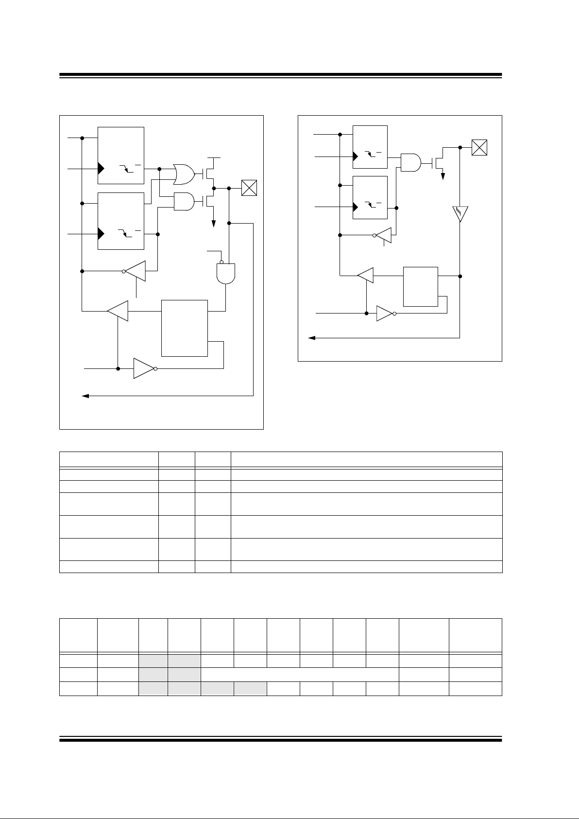
3.2 PORTB and the TRISB Register
PORTB is an 8-bit wide bi-directional port. The corresponding data direction register is TRISB. Setting a
TRISB bit (=1) will make the correspon ding POR TB pin
an input, i.e., put the corresponding output driver in a
hi-impedance mode. Clearing a TRISB bit (=0) will
make the corr espond ing PORTB pin an output, i.e., put
the contents of the output latch on the selected pin.
EXAMPLE 3-1: INITIALIZING PORTB
BCF STATUS, RP0 ;
CLRF PORTB ; Initialize PORTB by
; clearing output
; data latches
BSF STATUS, RP0 ; Select Bank 1
MOVLW 0xCF ; Value used to
; initialize data
; direction
MOVWF TRISB ; Set RB<3:0> as inputs
; RB<5:4> as outputs
; RB<7:6> as inputs
Each of the PORTB pins has a weak internal pull-up. A
single control bit ca n turn on all the pull-ups . This is performed by clearing bit RBPU (OPTION_REG<7>). The
weak pull-up i s automa tically tur ned off wh en the po rt
pin is configured as an output. The pull-ups are disabled on a Power-on Reset.
The RB0 pin is multiplexed with the external interrupt
(RB0/INT).
FIGURE 3-4: BLOCK DIAGRAM OF RB0 PIN
The RB1 pin is multiplexed with the SSP module slave
select (RB1/SS
).
FIGURE 3-5: BLOCK DIAGRAM OF RB1/SS
PIN
The RB2 pin is multiplexed with analog channel 8
(RB2/AN8).
FIGURE 3-6: BLOCK DIAGRAM OF
RB2/AN8 PIN
Data Latch
RBPU
(2)
P
V
DD
QD
CK
QD
CK
QD
EN
Data bus
WR Port
WR TRIS
RD TRIS
RD Port
weak
pull-up
RD Port
RB0/INT
I/O
pin
(1)
TTL
Input
Buffer
Note 1: I/O pins have diode protection to V
DD and VSS.
2: To enable weak pull-ups, set the appropriate TRIS bit(s)
and clear the RBPU
bit (OPTION_REG<7>).
Schmitt Trigger
Buffer
TRIS Latch
Data Latch
RBPU
(2)
P
V
DD
QD
CK
QD
CK
QD
EN
Data bus
WR Port
WR TRIS
RD TRIS
RD Port
weak
pull-up
RD Port
SS input
I/O
pin
(1)
TTL
Input
Buffer
Note 1: I/O pins have diode protection to V
DD and VSS.
2: To enable weak pull-ups, set the appropriate TRIS bit(s)
and clear the RBPU
bit (OPTION_REG<7>).
Schmitt Trigger
Buffer
TRIS Latch
Data Latch
RBPU
(2)
P
V
DD
QD
CK
QD
CK
QD
EN
Data bus
WR Port
WR TRIS
RD TRIS
RD Port
weak
pull-up
RD Port
To A/D converter
I/O
pin
(1)
TTL
Input
Buffer
Note 1: I/O pins have diode protection to V
DD and VSS.
2: To enable weak pull-ups, set the appropriate TRIS bit(s)
and clear the RBPU
bit (OPTION_REG<7>).
TRIS Latch
Analog
input mode

PIC16C77X
DS30275A-page 30 Advance Information 1999 Microchip Technology Inc.
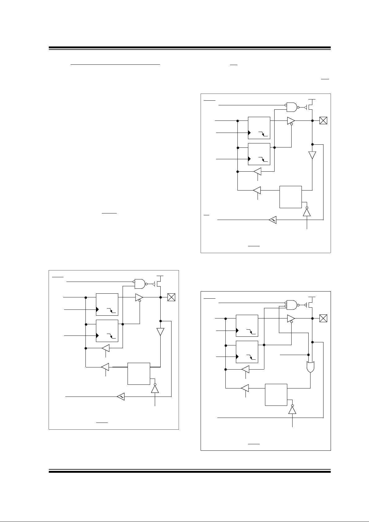
The RB3 pin is multiplexed with analog channel 9 and
the low voltage detect input (RB3/AN9/LVDIN)
FIGURE 3-7: BLOCK DIAGRAM OF
RB3/AN9/LVDIN PIN
Four of PORTB’s pins, RB7:RB4, have an interrupt on
change feature. Only pins configured as inputs can
cause this interrupt to oc cur (i.e . any RB7:RB4 pin configured as an output is excluded from the interrupt on
change comparison). The input pins (of RB7:RB4) are
compared with the old va lue latc hed on the la st read of
PORTB. The “mismatch” outputs of RB7:RB4 are
OR’ed together to generate the RB Port Change Interrupt with flag bit RBIF (INTCON<0>).
This interrupt can wake the device from SLEEP. The
user, i n the interrupt service routine , can clea r the interrupt in the following manner:
a) Any read or write of PORTB. This will end the
mismatch condition.
b) Clear flag bit RBIF.
A mismatch condition will continue to set flag bit RBIF.
Reading PORTB will end the mismatch condition, and
allow flag bit RBIF to be cleared.
The interrupt on change feature is recommended for
wake-up on key depression operation and opera tions
where PORTB is only used for the interrupt on change
feature. Polling of PORTB is not recommended while
using the interrupt on change feature.
FIGURE 3-8: BLOCK DIAGRAM OF
RB7:RB4 PINS
Data Latch
RBPU
(2)
P
V
DD
QD
CK
QD
CK
QD
EN
Data bus
WR Port
WR TRIS
RD TRIS
RD Port
weak
pull-up
RD Port
To A/D converter and LVD reference input
I/O
pin
(1)
TTL
Input
Buffer
Note 1: I/O pins have diode protection to V
DD and VSS.
2: To enable weak pull-ups, set the appropriate TRIS bit(s)
and clear the RBPU
bit (OPTION_REG<7>).
TRIS Latch
Analog
input mode
or LVD input
mode
Data Latch
From other
RBPU
(2)
P
V
DD
I/O
QD
CK
QD
CK
QD
EN
QD
EN
Data bus
WR Port
WR TRIS
Set RBIF
TRIS Latch
RD TRIS
RD Port
RB7:RB4 pins
weak
pull-up
RD Port
Latch
TTL
Input
Buffer
pin
(1)
Note 1: I/O pins have diode protection to VDD and VSS.
ST
Buffer
RB7:RB6 in serial programming mode
Q3
Q1
2: To enable weak pull-ups, set the appropriate TRIS bit(s)
and clear the RBPU
bit (OPTION_REG<7>).
 Loading...