

Microchip Technology Inc PIC16C745-I-SP, PIC16C745-JW, PIC16C745-I-SO, PIC16C765-I-P, PIC16C765-JW Datasheet

1999 Microchip Technology Inc.
Advanced Information DS41124A-page 1
Devices included in this data sheet:
Microcontroller Core Features:
• High-performance RISC CPU
• Only 35 single word instructions
• All single cycle instructions except for program
branches which are two cycle
• Interrupt capability (up to 12 internal/external
interrupt sources)
• Eight level deep hardware stack
• Direct, indirect and relative addressing modes
• Power-on Reset (POR)
• Power-up Timer (PWRT) and Oscillator Start-up
Timer (OST)
• Watchdog Timer (WDT) with its own on-chip RC
oscillator for reliable operation
• Brown-out detection circuitry for
Brown-out Reset (BOR)
• Programmable code-protection
• Power saving SLEEP mode
• Selectable oscillator options
- EC - External clock (24 MHz)
- E4 - External clock with PLL (6 MHz)
- HS - Crystal/Resonator (24 MHz)
- H4 - Crystal/Resonator with PLL (6 MHz)
• Processor clock of 24MHz derived from 6 MHz
crystal or resonator
• Fully static low-power, high-speed CMOS
• In-Circuit Serial Programming (ICSP)
• Operating voltage range
- 4.35 to 5.25V
• High Sink/Source Current 25/25 mA
• Wide temperature range
- Industrial (-40°C - 85°C)
• Low-power consumption:
- < TBD @ 5V, 6 MHz
- < TBD typical standby current
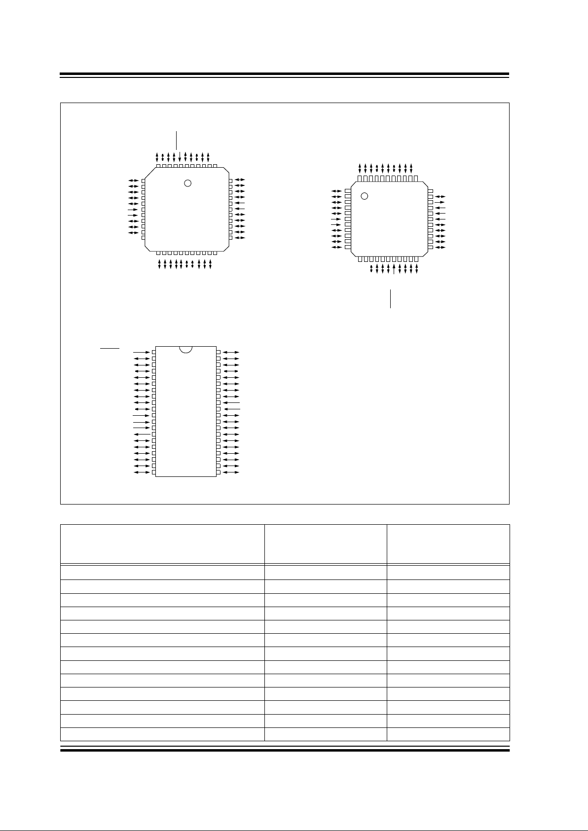
Pin Diagrams
Peripheral Features:
• Universal Serial Bus (USB 1.1)
• 64 bytes of USB dual port RAM
• 22 (PIC16C745) or 33 (PIC16C765) I/O pins
- Individual direction control
- 1 high voltage open drain (RA4)
- 8 PORTB pins with:
- Interrupt on change control (RB<7 :4> only)
- Weak pull up control
- 3 pins dedicated to USB
• Timer0: 8-bit timer/counter with 8-bit prescaler
• Timer1: 16-bit timer/counter with prescaler
can be incremented during sleep via external
crystal/clock
• Timer2: 8-bit timer/counter with 8-bit period
register, prescaler and postscaler
• 2 Capture, Compare and PWM modules
- Capture is 16 bit, max. resolution is 10.4 ns
- Compare is 16 bit, max. resolution is 167 ns
- PWM maximum resolution is 10 bit
• 8-bit multi-channel Analo g-to - Digi tal converter
• Universal Synchronous Asynchronous Receiver
Transmitter (USART/SCI)
• Parallel Slave Port (PSP) 8-bits wide, with external RD
, WR and CS controls (PIC16C765 only)
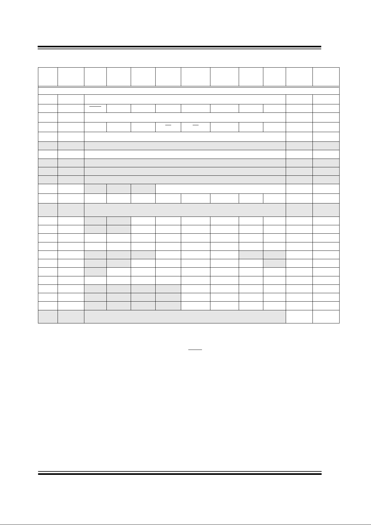
• PIC16C745 • PIC16C765
Device
Memory
Pins
A/D
Resolution
A/D
Channels
Program
x14
Data
x8
PIC16C745 8K 256 28 8 5
PIC16C765 8K 256 40 8 8
MCLR/VPP
RA0/AN0
RA1/AN1
RA2/AN2
RA3/AN3/V
REF
RA4/T0CKI
RA5/AN4
Vss
OSC1/CLKIN
OSC2/CLKOUT
RC0/T1OSO/T1CKI
RC1/T1OSI/CCP2
RC2/CCP1
V
USB
RB7
RB6
RB5
RB4
RB3
RB2
RB1
RB0/INT
V
DD
Vss
RC7/RX/DT
RC6/TX/CK
D+
D-
• 1
2
3
4
5
6
7
8
9
10
11
12
13
14
28
27
26
25
24
23
22
21
20
19
18
17
16
15
PIC16C745
28-Pin DIP, SOIC
PIC16C745/765
8-Bit CMOS Microcontrollers with USB
PIC16C745/765
DS41124A-page 2 Advanced Information
1999 Microchip Technology Inc.
RB3
RB2
RB1
RB0/INT
V
DD
VSS
RD7/PSP7
RD6/PSP6
RD5/PSP5
RD4/PSP4
RC7/RX/DT
RA4/T0CKI
RA5/AN4
RE0/RD/AN5
RE1/WR/AN6
RE2/CS/AN7
V
DD
VSS
OSC1/CLKIN
OSC2/CLKOUT
RC0/T1OSO/T1CKI
NC
RA3/AN3/VREF
RA2/AN2
RA1/AN1
RA0/AN0
MCLR
/VPP
NC
RB7
RB6
RB5
RB4
NC
7
8
9
10
11
12
13
14
15
16
17
39
38
37
36
35
34
33
32
31
30
29
NC
RC6/TX/CK
D+
D-
RD3/PSP3
RD2/PSP2
RD1/PSP1
RD0/PSP0
V
USB
RC2/CCP1
65432
1
4443424140
2827262524232221201918
PIC16C765
44-Pin PLCC
RC1/T1OSI/CCP2
NC
RC0/T1OSO/T1CKI
OSC2/CLKOUT
OSC1/CLKIN
V
SS
VDD
RE2/CS/AN7
RE1/WR/AN6
RE0/RD/AN5
RA5/AN4
RA4/T0CKI
RC7/RX/DT
RD4/PSP4
RD5/PSP5
RD6/PSP6
RD7/PSP7
V
SS
VDD
RB0/INT
RB1
RB2
RB3
RC6/TX/CK
D+D-RD3/PSP3
RD2/PSP2
RD1/PSP1
RD0/PSP0
V
USB
RC2/CCP1
RC1/T1OSI/CCP2
NC
1
2
3
4
5
6
7
8
9
10
11
33
32
31
30
29
28
27
26
25
24
23
RA3/AN3/VREF
RA2/AN2
RA1/AN1
RA0/AN0
MCLR
/VPP
RB7
RB6
RB5
RB4
NC
NC
4443424140393837363534
2221201918171615141312
PIC16C765
44-Pin TQFP
RB7
RB6
RB5
RB4
RB3
RB2
RB1
RB0/INT
V
DD
VSS
RD7/PSP7
RD6/PSP6
RD5/PSP5
RD4/PSP4
RC7/RX/DT
RC6/TX/CK
D+
DRD3/PSP3
RD2/PSP2
MCLR/VPP
RA0/AN0
RA1/AN1
RA2/AN2
RA3/AN3/V
REF
RA4/T0CKI
RA5/AN4
RE0/RD/AN5
RE1/WR/AN6
RE2/CS/AN7
V
DD
VSS
OSC1/CLKIN
OSC2/CLKOUT
RC0/T1OSO/T1CKI
RC1/T1OSI/CCP2
RC2/CCP1
V
USB
RD0/PSP0
RD1/PSP1
1
2
3
4
5
6
7
8
9
10
11
12
13
14
15
16
17
18
19
20
40
39
38
37
36
35
34
33
32
31
30
29
28
27
26
25
24
23
22
21
PIC16C765
40-Pin PDIP
Key Features
PICmicro
TM
Mid-Range Reference Manual
(DS33023)
PIC16C745 PIC16C765
Operating Frequency 6 MHz or 24 MHz 6 MHz or 24 MHz
Resets (and Delays) POR, BOR (PWRT, OST) POR, BOR (PWRT, OST)
Program Memory (14-bit words) 8K 8K
Data Memory (bytes) 256 256
Dual Port Ram 64 64
Interrupt Sources 11 12
I/O Ports 22 (Ports A, B, C) 33 (Ports A, B, C, D, E)
Timers 3 3
Capture/Compare/PWM modules 2 2
Analog-to-Digital Converter Module 5 channel x 8 bit 8 channel x 8 bit
Parallel Slave Port —Yes
Serial Communication USB, USART/SCI USB, USART/SCI
Brown Out Detect Reset Yes Yes

1999 Microchip Technology Inc.
Advanced Information DS41124A-page 3
PIC16C745/765
Table of Contents
1.0 General Description..............................................................................................................................................5
2.0 PIC16C745/765 Device Varieties .........................................................................................................................7
3.0 Architectural Overview .......................................................................................................................................... 9
4.0 Memory Organization..........................................................................................................................................15
5.0 I/O Ports..............................................................................................................................................................31
6.0 Timer0 Module....................................................................................................................................................43
7.0 Timer1 Module....................................................................................................................................................45
8.0 Timer2 Module....................................................................................................................................................49
9.0 Capture/Compare/PWM Modules.......................................................................................................................51
10.0 Universal Serial Bus............................................................................................................................................ 57
11.0 Universal Synchronous Asynchronous Receiver Transmitter (USART) .............................................................75
12.0 Analog-to-Digital Converter (A/D) Module ..........................................................................................................89
13.0 Special Features of the CPU..............................................................................................................................95
14.0 Instruction Set Summary...................................................................................................................................109
15.0 Development Support.......................................................................................................................................117
16.0 Electrical Characteristics.......................... ...... ...... ..... ...... ................................................................... ...... ..... ....123
17.0 DC and AC Characteristics Graphs and Tables ...............................................................................................141
18.0 Packaging Information...................................................................................................................................... 143
Index ..........................................................................................................................................................................151
On-Line Support..........................................................................................................................................................155
Reader Response....................................................................................................................................................... 156
Product Identification System .....................................................................................................................................157
To Our Va lued Customers
Most Current Data Sheet
To obtain the most up-to-date version of this data sheet, please register at our Worldwide Web site at:
http://www.microchip.com
You can determine the version of a data sheet by examining its literature number found on the bottom outside corner of any page.
The last character of the literature number is the ver sion number. e.g., DS30000A is version A of document DS30000.
New Customer Notification System
Register on our web site (www.microchip.com/ cn) to receive the most current information on our products.
Errata
An errata sheet may exist for current devices, describing minor operational differences (from the data sheet) and recommended
workarounds. As device/documentation issues become known to us, w e will pub lish an errata sheet. The errata will specify the re vision of silicon and revision of document to which it applies.
To determine if an errata sheet exists for a particular device, please check with one of the following:
• Microchip’s Worldwide Web site; http://www.microchip.com
• Your local Microchip sales office (see last page)
• The Microchip Corporate Literature Center; U.S. FAX: (480) 786-7277
When contacting a sales office or the literature center, please specify which device, revision of silicon and data sheet (include liter-
ature number) you are using.
Corrections to this Data Sheet
We constantly strive to improve the quality of all our products and documentation. We have spent a great deal of time to ensure
that this document is correct. However , w e realize that we ma y have missed a few things. If y ou find any inf ormation that is missing
or appears in error, please:
• Fill out and mail in the reader response form in the back of this data sheet.
• E-mail us at webmaster@microchip.com.
We appreciate your assistance in making this a better document.

PIC16C745/765
DS41124A-page 4 Advanced Information
1999 Microchip Technology Inc.
NOTES:

1999 Microchip Technology Inc.
Advanced Information DS41124A-page 5
PIC16C745/765
1.0 GENERAL DESCRIPTION
The PIC16C745/765 devices are lo w-cost, high-perf or-
mance, CMOS, fully-static, 8-bit microcontrollers in the
PIC16CXX mid-range family.
All PICmicro
®
microcontrollers employ an advanced
RISC architecture. The PIC16CXX micro controller family has enhanced core features, eight-level deep stack
and multiple internal and external interrupt sources.
The separate instruction and data buses of the Harvard
architecture allow a 14-bit wide instruction word with
the separate 8-bit wide data. The two stage instruction
pipeline allows all instructions to execute in a single
cycle, except for program branches, which require two
cycles. A total of 35 instructions (reduced instruction
set) are avai lable. Ad ditionally, a large register set give s
some of the architectur al inno v ations us ed to achie v e a
very high performance.
The PIC16C745 device has 22 I/O pins. The
PIC16C765 device has 33 I/O pins. Each device has
256 bytes of RAM. In addition, several peripheral features are available including: three timer/counters, two
Capture/Compare/PWM modules and two serial ports.
The Universal Serial Bus (USB 1.1) peripheral provides bus communications. The Universal Synchronous Asynchronous Receiver Transmitter (USART) is
also known as the Serial Communications Interface or
SCI. Also, a 5-channel high-speed 8-bit A/D is provided on the PIC16C745, while the PIC16C765 offers
8 channels. The 8-bit resolution is ideally suited for
applications requiring a low-cost analog interface,
(e.g., thermostat control, pressure sensing, etc).
The PIC16C745/765 devices have special features to
reduce external components, thus reducing cost,
enhancing system reliability and reducing power consumption. There are 4 o scillator options , of whic h EC is
for the external regulated clock source, E4 is for the
external regulated clock source with PLL, HS is for the
high speed crystals/resonators and H4 is for high
speed crystals/resontators with PLL. The SLEEP
(power-down) feature provides a power-saving mode.
The user can wake up the chip from SLEEP through
several external and internal interrupts and resets.
A highly reliable Watchdog Timer (WDT), with a dedicated on-chip RC oscill ator, pr ovides protec tion against
software lock-up, and also provides one way of waking
the device from SLEEP.
A UV erasable CERDIP packaged version is ideal for
code development, while the cost-effective One-Ti meProgrammable (OTP) version is suitable for production
in any volume.
The PIC16C745/765 devices fit nicely in many applications ranging from security and remote sensors to appliance controls and automotives. The EPROM
technology makes customization of application programs (data loggers, industrial controls, UPS) extremely
fast and convenient. The small footprint packages make
this microcontroller series perfect for all applications
with space limitations. Low cost, low power, high performance, ease of use and I/O flexibility make the
PIC16C745/765 devices very versatile, even in areas
where no microcontroller use has been considered
before (e.g., timer functions, serial communication, capture and compare, PWM functions and coprocessor
applications).
1.1 Family and Upward Compatibility
Users familiar with the PIC16C5X microcontroller family will realize that this is an enhanced version of the
PIC16C5X architecture. Code written for the
PIC16C5X can be easil y p orted to the PIC16 CXX family of devices.
1.2 Development Support
PICmicro® devices are supported by the complete line
of Microchip Development tools.
Please refer to Section 15.0 for more details about
Microchip’s development tools.

PIC16C745/765
DS41124A-page 6 Advanced Information
1999 Microchip Technology Inc.
NOTES:

1999 Microchip Technology Inc.
Advanced Information DS41124A-page 7
PIC16C745/765
2.0 PIC16C745/765 DEVICE
VARIETIES
A variety of frequency ranges and packaging options
are avai lable . Dependin g on application an d production
requirements, th e proper de vice option ca n be selected
using the information in the PIC16C745/765 Product
Identification System section at the end of this data
sheet. When placing orders, please use that page of
the data sheet to specify the correct part number.
2.1 UV Erasable Devices
The UV erasable version, offered in windowed CERDIP
packages (600 mil), is optimal for prototype development and pilot programs. This version can be erased
and reprogrammed to any of the supported oscillator
modes.
Microchip’s PICSTART
Plus and PROMATEII
programmers both support programming of the
PIC16C745/765.
2.2 One-Time-Programmable (OTP)
Devices
The availability of OTP devices is especially useful for
customers who need the flexibility for frequent code
updates and small volume applications.
The OTP devices, packaged in plastic packages, permit the user to program them once. In addition to the
program memory, the configuration bits must also be
programmed.
2.3 Quick-Turnaround-Production (QTP)
Devices
Microchip offers a QTP Programming Service for factory production orders. This service is made available
for users who choose not to program a medium to high
quantity of units and whose code patterns have stabilized. The devices are identical to the OTP devices but
with all EPROM locations and configuration options
already programmed by the factory. Certain code and
prototype verification procedures apply before production shipments are available. Please contact your local
Microchip Technology sales office for more details.
2.4 Serialized Quick-Turnaround
Production (SQTPSM) Devices
Microchip offers a unique programming service where
a few user-defined locations in each device are programmed with different serial numbers. The serial numbers may be rando m, ps eud o-random or sequential.
Serial programming allows each device to have a
unique number, which can serve as an entry-code,
password or ID number.

PIC16C745/765
DS41124A-page 8 Advanced Information
1999 Microchip Technology Inc.
NOTES:

1999 Microchip Technology Inc.
Advanced Information DS41124A-page 9
PIC16C745/765
3.0 ARCHITECTURAL OVERVIEW
The high performance of the PIC16CXX family can be
attributed to a number of arch itectural features commonly found in RISC microprocessor s. To begin w ith,
the PIC16CXX uses a Har vard architecture, in which
program and data are accessed from separate memories using separate buses. This improves bandwidth
over tr aditional von Neu mann archi tecture in wh ich program and data are fetched from the same memory
using the same bus. Separating program and data
buses further allows instructions to be sized differently
than the 8-bit wide data word. Instruction opcodes are
14-bits wid e maki ng it po ssible to h ave all singl e word
instructions. A 14-bit wide program memory access
bus fet ches a 14 -bit ins truction in a si ngle cy cle . A tw ostage pipeline overlaps fetch and execution of instructions (Example 3-1). Consequently, most instructions
execute in a single cycle (166.6667 ns @ 24 MHz)
except for program branches.
The PIC16CXX can directly or indirectly address its
register files or data memory. Al l s pec ia l function registers, including the program counter, are mapped in the
data memory . The PIC16CXX has an orthogonal (symmetrical) ins tr ucti on s et th at m akes it po ssible to c arr y
out any operatio n on any reg ister usin g any add ressing
mode. This symmetrical nature and lack of ‘special
optimal situations’ make programming with the
PIC16CXX simple yet e fficient. In addition, the learning
curve is reduced significantly.
PIC16CXX devices contain an 8-bit ALU and working
register. The ALU is a general purpose arithmetic unit.
It performs arithmetic and Boolean functions between
the data in the working register and any register file.
The ALU is 8-bits wide and capable of addition, subtraction, shift and logical operations. Unless otherwise
mentioned, arithmetic operations are two's complement in nature. In two-operand instructions, typically
one operand is the working register (W register). The
other operand is a file register or an immediate constant. In single operand instructions, the operand is
either the W register or a file register.
The W register is an 8-bit working register use d for ALU
operations. It is not an addressable register.
Depending on the instruction executed, the ALU may
affect the v alues of th e Ca rry (C), Digit Carry (DC), an d
Zero (Z) bits in the STATUS register . The C and DC bits
operate as a borrow
bit and a digit borrow out bit,
respectively, in subtra cti on. See the SUBLW and SUBWF
instructions for examples.
Device
Memory
Pins
A/D
Resolution
A/D
Channels
Program
x14
Data
x8
PIC16C745 8K 256 28 8 5
PIC16C765 8K 256 40 8 8
PIC16C745/765
DS41124A-page 10 Advanced Information
1999 Microchip Technology Inc.
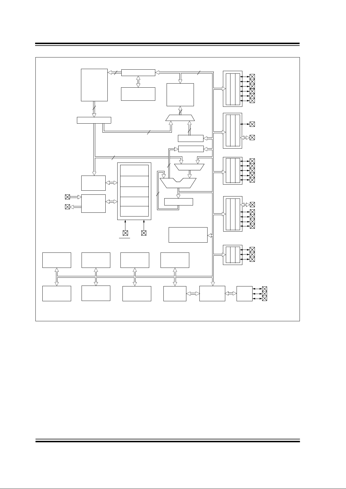
FIGURE 3-1: PIC16C745/765 BLOCK DIAGRAM
13
Data Bus
8
14
Program
Bus
Instruction reg
Program Counter
8 Level Stack
(13 bit)
Direct Addr
7
RAM Addr(1)
9
Addr MUX
Indirect
Addr
FSR reg
STATUS reg
MUX
ALU
W reg
Power-up
Timer
Oscillator
Start-up Timer
Power-on
Reset
Watchdog
Timer
Instruction
Decode &
Control
Timing
Generation
OSC1/
OSC2/
MCLR
VDD, VSS
PORTA
PORTB
PORTC
PORTD
PORTE
RA4/T0CKI
RA5/AN4
RB0/INT
RB<7:1>
RC0/T1OSO/T1CKI
RC1/T1OSI/CCP2
RC2/CCP1
V
USB
DD+
RC6/TX/CK
RC7/RX/DT
RD3:0/PSP3:0
(2)
RE0/AN5/RD
(2)
RE1/AN6/WR
(2)
8
8
Brown-out
Reset
Note 1: Higher order bits are from the STATUS register.
2: Not available on PIC16C745.
USART
CCP1
8-bit A/DTimer0 Timer1 Timer2
RA3/AN3/VREF
RA2/AN2
RA1/AN1
RA0/AN0
Parallel Slave Port
(2)
8
3
RD4/PSP4
(2)
RD5/PSP5
(2)
RD6/PSP6
(2)
RD7/PSP7
(2)
USB
CLKOUT
CLKIN
CCP2
XCVR
RAM
File
Registers
256 x 8
Dual Port
EPROM
Program
Memory
8K x 14
RAM
64 x 8
x4 PLL
RE2/AN7/CS
(2)

1999 Microchip Technology Inc.
Advanced Information DS41124A-page 11
PIC16C745/765
TABLE 3-1: PIC16C745/765 PINOUT DESCRIPTION
Name Function
Input
Type
Output
Type
Description
MCLR
/VPP
MCLR ST — Master Clear
V
PP Power — Programming Voltage
OSC1/CLKIN
OSC1 Xtal — Crystal/Resonator
CLKIN ST — External Clock Input/ER resistor connection.
OSC2/CLKOUT
OSC2 — Xtal Crystal/Resonator
CLKOUT — CMOS Internal Clock (F
INT/4) Output
RA0/AN0
RA0 ST CMOS Bi-directional I/O
AN0 AN — A/D Input
RA1/AN1
RA1 ST CMOS Bi-directional I/O
AN1 AN — A/D Input
RA2/AN2
RA2 ST CMOS Bi-directional I/O
AN2 AN — A/D Input
RA3/AN3/V
REF
RA3 ST CMOS Bi-directional I/O
AN3 AN — A/D Input
V
REF AN — A/D Positive Reference
RA4/T0CKI
RA4 ST OD Bi-directional I/O
T0CKI ST — Timer 0 Clock Input
RA5/AN4
RA5 ST Bi-directional I/O
AN4 AN — A/D Input
RB0/INT
RB0 TTL CMOS Bi-directional I/O
INT ST — Interrupt
RB1 RB1 TTL CMOS Bi-directional I/O
RB2 RB2 TTL CMOS Bi-directional I/O
RB3 RB3 TTL CMOS Bi-directional I/O
RB4 RB4 TTL CMOS Bi-directional I/O with Interrupt on Change
RB5 RB5 TTL CMOS Bi-directional I/O with Interrupt on Change
RB6/ICSPC
RB6 TTL CMOS Bi-directional I/O with Interrupt on Change
ICSPC ST In-Circuit Serial Programming Clock input
RB7/ICSPD
RB7 TTL CMOS Bi-directional I/O with Interrupt on Change
ICSPD ST CMOS In-Circuit Serial Programming Data I/O
RC0/T1OSO/T1CKI
RC0 ST CMOS Bi-directional I/O
T1OSO — Xtal T1 Oscillator Output
T1CKI ST — T1 Clock Input
RC!/T1OSI/CCP2
RC1 ST CMOS Bi-directional I/O
T1OSI Xtal — T1 Oscillator Input
CCP2 Capture In/Compare Out/PWM Out 2
RC2/CCP1/V
USB
RC2 ST CMOS Bi-directional I/O
CCP1 Capture In/Compare Out/PWM Out 1
V
USB VUSB Power 3.3V for pull up resistor
D- D- USB USB USB Differential Bus
D+ D+ USB USB USB Differential Bus
Legend: OD = open drain, ST = Schmitt Trigger
Note 1: Weak pull-ups. PORT B pull-ups are byte wide programmable.
2: PIC16C765 only.

PIC16C745/765
DS41124A-page 12 Advanced Information
1999 Microchip Technology Inc.
RC6/TX/CK
RC6 ST CMOS Bi-directional I/O
TX — CMOS USART Async Transmit
CK ST CMOS USART Master Out/ Slave In Clock
RC7/RX/DT
RC7 ST CMOS Bi-directional I/O
RX ST — USART Async Receive
DT ST CMOS USART Data I/O
RD0/PSP0
RD0 TTL CMOS Bi-directional I/O
(2)
PSP0 TTL — Parallel Slave Port data input
(2)
RD1/PSP1
RD1 TTL CMOS Bi-directional I/O
(2)
PSP1 TTL — Parallel Slave Port data input
(2)
RD2/PSP2
RD2 TTL CMOS Bi-directional I/O
(2)
PSP2 TTL — Parallel Slave Port data input
(2)
RD3/PSP3
RD3 TTL CMOS Bi-directional I/O
(2)
PSP3 TTL — Parallel Slave Port data input
(2)
RD4/PSP4
RD4 TTL CMOS Bi-directional I/O
(2)
PSP4 TTL — Parallel Slave Port data input
(2)
RD5/PSP5
RD5 TTL CMOS Bi-directional I/O
(2)
PSP5 TTL — Parallel Slave Port data input
(2)
RD6/PSP6
RD6 TTL CMOS Bi-directional I/O
(2)
PSP6 TTL — Parallel Slave Port data input
(2)
RD7/PSP7
RD7 TTL CMOS Bi-directional I/O
(2)
PSP7 TTL — Parallel Slave Port data input
(2)
RE0/RD/AN5
RE0 ST CMOS Bi-directional I/O
(2)
RD TTL — Parallel Slave Port control input
(2)
AN5 AN — A/D Input
(2)
RE1/WR/AN6
RE1 ST CMOS Bi-directional I/O
(2)
WR TTL — Parallel Slave Port control input
(2)
AN6 AN — A/D Input
(2)
RE2/CS/AN7
RE2 ST CMOS Bi-directional I/O
(2)
CS TTL — Parallel Slave Port data input
(2)
AN7 AN — A/D Input
(2)
VDD VDD Power — Power
V
SS VSS Power — Ground
AV
DD AVDD Power — Analog Power
AV
SS AVSS Power — Analog Ground
TABLE 3-1: PIC16C745/765 PINOUT DESCRIPTION (CONTINUED)
Name Function
Input
Type
Output
Type
Description
Legend: OD = open drain, ST = Schmitt Trigger
Note 1: Weak pull-ups. PORT B pull-ups are byte wide programmable.
2: PIC16C765 only.
1999 Microchip Technology Inc.
Advanced Information DS41124A-page 13
PIC16C745/765
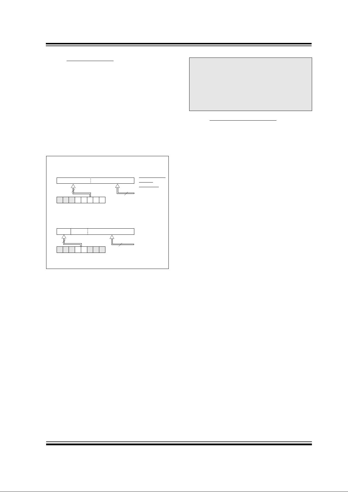
3.1 Clocking Scheme/Instruction Cycle
The clock input feeds an on-chip PLL. The clock output
from the PLL (F
INT) is internally divided by four to gen-
erate four non-overlapping quadrature clocks namely,
Q1, Q2, Q3 and Q4. Internally, the program counter
(PC) is incremented e very Q1, the instruction is f etched
from the program memory and latched into the instruction register in Q4. The ins truction is decod ed and executed during the following Q1 through Q4. The clocks
and instruction execution flow is shown in Figure 3-2.
3.2 Instruction Flow/Pipelining
An “Instruction Cycle” consists of four Q cycles (Q1,
Q2, Q3 and Q4). The instruction fetch and execute are
pipelined such that fetch takes one instruction cycle,
while decode and execute takes another instruction
cycle. However, due to the pipelining, each instruction
effectively executes in one cycle. If an instruction
causes the program counter to change (e.g., GOTO),
then two cycles are required t o complete t he instruction
(Example 3-1).
A fetch cycle begins with the program counter (PC)
incrementing in Q1.
In the ex ecu tion cycle , t he f etched i nstruction i s latche d
into the “Instruction Register" (IR) in cycle Q1. This
instruction is then decoded and executed during the
Q2, Q3 and Q4 cycles . Data mem ory is read during Q2
(operand read) and written during Q4 (destination
write).
FIGURE 3-2: CLOCK/INSTRUCTION CYCLE
EXAMPLE 3-1: INSTRUCTION PIPELINE FLOW
Q1
Q2 Q3 Q4
Q1
Q2 Q3 Q4
Q1
Q2 Q3 Q4
FINT
Q1
Q2
Q3
Q4
PC
OSC2/CLKOUT
(EC mode)
PC PC+1 PC+2
Fetch INST (PC)
Execute INST (PC-1) Fetch INST (PC+1)
Execute INST (PC) Fetch INST (PC+2)
Execute INST (PC+1)
Internal
phase
clock
Note: All instructions are single cycle, except for any program branches. These take two cycles, since the fetch
instruction is “flushed ” from the pipeline, while the new instruction is being fetched and then executed.
TCY0TCY1TCY2TCY3TCY4TCY5
1. MOVLW 55h
Fetch 1 Execute 1
2. MOVWF PORTB
Fetch 2 Execute 2
3. CALL SUB_1
Fetch 3 Execute 3
4. BSF PORTA, BIT3 (Forced NOP)
Fetch 4 Flush
5. Instruction @ address SUB_1
Fetch SUB_1 Execute SUB_1

PIC16C745/765
DS41124A-page 14 Advanced Information
1999 Microchip Technology Inc.
NOTES:
1999 Microchip Technology Inc.
Advanced Information DS41124A-page 15
PIC16C745/765
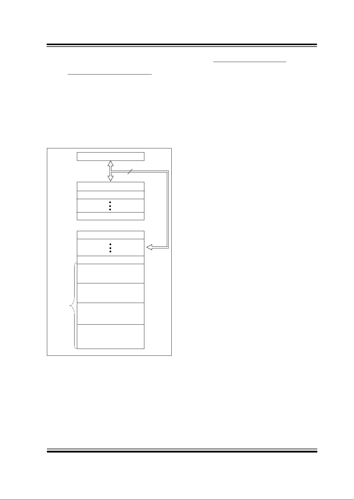
4.0 MEMORY ORGANIZATION
4.1 Program Memory Organization
The PIC16C745/765 has a 13-bit program counter
capable of addressing an 8K x 14 program memory
space. All devices covered by this datasheet have 8K x
14 bits of program memory. The address range is
0000h - 1FFFh for all devices.
The reset vector is at 0000h and the interrupt vector is
at 0004h.
FIGURE 4-1: PIC16C745/765 PROGRAM
MEMORY MAP AND STACK
4.2 Data Memory Organization
The data memory is partitioned into multiple banks
which contain the General Purpose Registers (GPR)
and the Special Function Registers (SFR). Bits RP1
and RP0 are the bank select bits.
RP<1:0> (STATUS<6:5>)
= 00 → Bank0
= 01 → Bank1
= 10 → Bank2
= 11 → Bank3
Each bank extends up to 7Fh (128 bytes). The lower
locations of each bank are reserved for the SFRs.
Above the SFRs are GPRs, implemented as static
RAM.
All implemented ban ks co ntain SF Rs. Some “h igh us e”
SFRs from one bank may be mirrored in another bank
for code reduction and quicker access.
4.2.1 GENERAL PURPOSE REGISTER FILE
The register file can be ac cess ed eithe r dire ctly o r indi-
rectly through the File Select Register (FSR)
(Section 4.5).
PC<12:0>
13
0000h
0004h
0005h
Stack Level 1
Stack Level 8
Reset Vector
Interrupt Vector
On-chip
CALL, RETURN
RETFIE, RETLW
Stack Level 2
Program
Memory
Page 0
Page 1
07FFh
0800h
0FFFh
1000h
Page 2
1800h
17FFh
Page 3
1FFFh
PIC16C745/765
DS41124A-page 16 Advanced Information
1999 Microchip Technology Inc.
FIGURE 4-2: DATA MEMORY MAP FOR PIC16C745/765
Bank 0 File
Address
Bank 1 File
Address
Bank 2 File
Address
Bank 3 File
Address
Indirect addr.(*) 00h Indirect addr.(*) 80h Indirect addr.(*) 100h Indirect addr.(*) 180h
TMR0 01h OPTION_REG 81h TMR0 101h OPTION_REG 181h
PCL 02h PCL 82h PCL 102h PCL 182h
STATUS 03h STATUS 83h STATUS 103h STATUS 183h
FSR 04h FSR 84h FSR 104h FSR 184h
PORTA 05h TRISA 85h
105h 185h
PORTB 06h TRISB 86h PORTB 106h TRISB 186h
PORTC 07h TRISC 87h
107h 187h
PORTD
(2)
08h
TRISD
(2)
88h 108h 188h
PORTE
(2)
09h
TRISE
(2)
89h 109h 189h
PCLATH 0Ah PCLATH 8Ah PCLATH 10Ah PCLATH 18Ah
INTCON 0Bh INTCON 8Bh INTCON 10Bh INTCON 18Bh
PIR1 0Ch PIE1 8Ch
10Ch 18Ch
PIR2 0Dh PIE2 8Dh
10Dh 18Dh
TMR1L 0Eh PCON 8Eh
10Eh 18Eh
TMR1H 0Fh
8Fh 10Fh 18Fh
T1CON 10h
90h 110h UIR 190h
TMR2 11h
91h 111h UIE 191h
T2CON 12h PR2 92h
112h UEIR 192h
13h 93h 113h UEIE 193h
14h 94h 114h USTAT 194h
CCPR1L 15h
95h 115h UCTRL 195h
CCPR1H 16h
96h 116h UADDR 196h
CCP1CON 17h
97h 117h
USWSTAT
(1)
197h
RCSTA 18h TXSTA 98h
118h UEP0 198h
TXREG 19h SPBRG 99h
119h UEP1 199h
RCREG 1Ah
9Ah 11Ah UEP2 19A h
CCPR2L 1Bh
9Bh 11Bh
19Bh
(1)
CCPR2H 1Ch 9Ch 11Ch
19Ch
(1)
CCP2CON 1Dh 9Dh 11Dh
19Dh
(1)
ADRESH 1Eh 9Eh 11Eh
19Eh
(1)
ADCON0 1Fh ADCON1 9Fh 11Fh
19Fh
(1)
General
Purpose
Register
96 Bytes
20h General
Purpose
Register
80 Bytes
A0h General
Purpose
Register
80 Bytes
120h USB Dual Port
Memory
64 Bytes
1A0h
1DFh
1E0h
EFh 16Fh 1EFh
accesses
70h-7Fh
F0h accesses
70h-7Fh
170h accesses
70h-7Fh
1F0h
7Fh FFh 17Fh 1FFh
Unimplemented data memory locations, read as ‘0’.
*Not a physical register.
Note 1: Reserved registers may contain USB state information.
2: Parallel slave ports (PORTD and PORTE) not implemented on PIC16C745; always maintain these bits clear.
1999 Microchip Technology Inc.
Advanced Information DS41124A-page 17
PIC16C745/765
4.2.2 SPECIAL FUNCTION REGISTERS
The Special Function Registers are registers used by
the CPU and Peripheral Modules for controlling the
desired operation of the device. These registers are
implemented as static RAM.
The Special Function Registers can be classified into
two sets (core and periphe ra l). Those registers associ-
ated with the “core” func tions are described i n this section, and those related to the operation of the peripheral
features are described in the section of that peripheral
feature.
TABLE 4-1: SPECIAL FUNCTION REGISTER SUMMARY
Address Name Bit 7 Bit 6 Bit 5 Bit 4 Bit 3 Bit 2 Bit 1 Bit 0
Value on:
POR,
BOR
Value on all
other resets
(2)
Bank 0
00h INDF
(3)
Addressing this location uses contents of FSR to address data memory (not a physical register) 0000 0000 0000 0000
01h TMR0 Timer0 module’s register xxxx xxxx uuuu uuuu
02h PCL
(3)
Program Counter's (PC) Least Significant Byte 0000 0000 0000 0000
03h STATUS
(3)
IRP
(2)
RP1
(2)
RP0 TO PD ZDCC0001 1xxx 000q quuu
04h FSR
(3)
Indirect data memory address pointer xxxx xxxx uuuu uuuu
05h PORTA
— — PORTA Data Latch when written: PORTA pins when read --0x 0000 --0u 0000
06h PORTB PORTB Data Latch when written: PORTB pins when read xxxx xxxx uuuu uuuu
07h PORTC
RC7 RC6
— — —
RC2 RC1 RC0
xx-- -xxx uu-- -uuu
08h PORTD
(4)
PORTD Data Latch when written: PORTD pins when read xxxx xxxx uuuu uuuu
09h PORTE
(4)
— — — — — RE2 RE1 RE0 ---- -xxx ---- -uuu
0Ah PCLATH
(1,3)
— — — Write Buffer for the upper 5 bits of the Program Counter ---0 0000 ---0 0000
0Bh INTCON
(3)
GIE PEIE T0IE INTE RBIE T0IF INTF RBIF 0000 000x 0000 000u
0Ch PIR1 PSPIF
(4)
ADIF RCIF TXIF USBIF CCP1IF TMR2IF TMR1IF 0000 0000 0000 0000
0Dh PIR2
— — — – — — — CCP2IF ---- ---0 ---- ---0
0Eh TMR1L Holding register for the Least Significant Byte of the 16-bit TMR1 register xxxx xxxx uuuu uuuu
0Fh TMR1H Holding register for the Most Significant Byte of the 16-bit TMR1 register xxxx xxxx uuuu uuuu
10h T1CON
— — T1CKPS1 T1CKPS0 T1OSCEN T1SYNC TMR1CS TMR1ON --00 0000 --uu uuuu
11h TMR2 Timer2 module’s register 0000 0000 0000 0000
12h T2CON
— TOUTPS3 TOUTPS2 TOUTPS1 TOUTPS0 TMR2ON T2CKPS1 T2CKPS0 -000 0000 -000 0000
13h — Unimplemented — —
14h — Unimplemented — —
15h CCPR1L Capture/Compare/PWM Register1 (LSB) xxxx xxxx uuuu uuuu
16h CCPR1H Capture/Compare/PWM Register1 (MSB) xxxx xxxx uuuu uuuu
17h CCP1CON
— — DC1B1 DC1B0 CCP1M3 CCP1M2 CCP1M1 CCP1M0 --00 0000 --00 0000
18h RCSTA SPEN RX9 SREN CREN
— FERR OERR RX9D 0000 -00x 0000 -00x
19h TXREG USART T r ansmit Data Register 0000 0000 0000 0000
1Ah RCREG USART Receive Data Register 0000 0000 0000 0000
1Bh CCPR2L Capture/Compare/PWM Register2 (LSB) xxxx xxxx uuuu uuuu
1Ch CCPR2H Capture/Compare/PWM Register2 (MSB) xxxx xxxx uuuu uuuu
1Dh CCP2CON
— — DC2B1 DC2B1 CCP2M3 CCP2M2 CCP2M1 CCP2M0 --00 0000 --00 0000
1Eh ADRES A/D Result Register xxxx xxxx uuuu uuuu
1Fh ADCON0 ADCS1 ADCS0 CHS2 CHS1 CHS0 GO/DONE
—ADON0000 00-0 0000 00-0
Legend:x = unknown, u = unchanged, q = value depends on condition, - = unimplemented read as ’0’.
Shaded locations are unimplemented, read as ‘0’.
Note 1: The upper byte of the program counter is not directly accessible. PCLATH is a holding register for the PC<12:8> whose contents
are transferred to the upper byte of the program counter.
2: Other (non power-up) resets include external reset through MCLR
and Watchdog Timer Reset.
3: These registers can be addressed from either bank.
4: The Parallel Slave Port (PORTD and PORTE) is not implemented on the PIC16C745, always maintain these bits clear.
PIC16C745/765
DS41124A-page 18 Advanced Information
1999 Microchip Technology Inc.
Bank 1
80h INDF
(3)
Addressing this location uses contents of FSR to address data memory (not a physical register) 0000 0000 0000 0000
81h OPTION RBPU
INTEDG T0CS T0SE PSA PS2 PS1 PS0 1111 1111 1111 1111
82h PCL
(3)
Program Counter’s (PC) Least Significant Byte 0000 0000 0000 0000
83h STATUS
(3)
IRP RP1 RP0 TO PD ZDCC0001 1xxx 000q quuu
84h FSR
(3)
Indirect data memory address pointer xxxx xxxx uuuu uuuu
85h TRISA
— — PORTA Data Direction Register --11 1111 --11 1111
86h TRISB PORTB Data Direction Register 1111 1111 1111 1111
87h TRISC
TRISC7 TRISC8
— — —
TRISC2 TRI SC1 TRISC0
11-- -111 11-- -111
88h TRISD
(4)
PORTD Data Direction Register 1111 1111 1111 1111
89h TRISE
(4)
IBF OBF IBOV PSPMODE — PORTE Data Direction Bits 0000 -111 0000 -111
8Ah PCLATH
(1,3)
— — — Write Buffer for the upper 5 bits of the Program Counter ---0 0000 ---0 0000
8Bh INTCON
(3)
GIE PEIE T0IE INTE RBIE T0IF INTF RBIF 0000 000x 0000 000u
8Ch PIE1 PSPIE
(4)
ADIE RCIE TXIE USBIE CCP1IE TMR2IE TMR1IE 0000 0000 0000 0000
8Dh PIE2
— — — — — — —CCP2IE---- ---0 ---- ---0
8Eh PCON
— — — — — —PORBOR ---- --qq ---- --uu
8Fh — Unimplemented — —
90h — Unimplemented — —
91h — Unimplemented — —
92h PR2 Timer2 Period Register 1111 1111 1111 1111
93h — Unimplemented — —
94h — Unimplemented — —
95h — Unimplemented — —
96h — Unimplemented — —
97h — Unimplemented — —
98h TXSTA CSRC TX9 T XEN SYNC
— BRGH TRMT TX9D 0000 -010 0000 -010
99h SPBRG Baud Rate Generator Register 0000 0000 0000 0000
9Ah — Unimplemented — —
9Bh — Unimplemented — —
9Ch — Unimplemented — —
9Dh — Unimplemented — —
9Eh — Unimplemented — —
9Fh ADCON1
— — — — — PCFG2 PCFG1 PCFG0 ---- -000 ---- -000
TABLE 4-1: SPECIAL FUNCTION REGISTER SUMMARY (CONTINUED)
Address Name Bit 7 Bit 6 Bit 5 Bit 4 Bit 3 Bit 2 Bit 1 Bit 0
Value on:
POR,
BOR
Value on all
other resets
(2)
Legend:x = unknown, u = unchanged, q = value depends on condition, - = unimplemented read as ’0’.
Shaded locations are unimplemented, read as ‘0’.
Note 1: The upper byte of the program counter is not directly accessible. PCLATH is a holding register for the PC<12:8> whose contents
are transferred to the upper byte of the program counter.
2: Other (non power-up) resets include external reset through MCLR
and Watchdog Timer Reset.
3: These registers can be addressed from either bank.
4: The Parallel Slave Port (PORTD and PORTE) is not implemented on the PIC16C745, always maintain these bits clear.
1999 Microchip Technology Inc.
Advanced Information DS41124A-page 19
PIC16C745/765
Bank 2
100h
INDF
(3)
Addressing this location uses contents of FSR to address data memory (not a physical register) 0000 0000 0000 0000
101h TMR0 Timer0 module’s register xxxx xxxx uuuu uuuu
102h
PCL
(3)
Program Counter's (PC) Least Significant Byte 0000 0000 0000 0000
103h
ST ATUS
(3)
IRP RP1 RP0 TO PD ZDCC0001 1xxx 000q quuu
104h
FSR
(3)
Indirect data memory address pointer xxxx xxxx uuuu uuuu
105h — Unimplemented — —
106h PORTB PORTB Data Latch when written: PORTB pins when read xxxx xxxx uuuu uuuu
107h — Unimplemented — —
108h — Unimplemented — —
109h — Unimplemented — —
10Ah
PCLATH
(1,3)
— — — Write Buffer for the upper 5 bits of the Program Counter ---0 0000 ---0 0000
10Bh
INTCON
(3)
GIE PEIE T0IE INTE RBIE T0IF INTF RBIF 0000 000x 0000 000u
10Ch11Fh
— Unimplemented — —
TABLE 4-1: SPECIAL FUNCTION REGISTER SUMMARY (CONTINUED)
Address Name Bit 7 Bit 6 Bit 5 Bit 4 Bit 3 Bit 2 Bit 1 Bit 0
Value on:
POR,
BOR
Value on all
other resets
(2)
Legend:x = unknown, u = unchanged, q = value depends on condition, - = unimplemented read as ’0’.
Shaded locations are unimplemented, read as ‘0’.
Note 1: The upper byte of the program counter is not directly accessible. PCLATH is a holding register for the PC<12:8> whose contents
are transferred to the upper byte of the program counter.
2: Other (non power-up) resets include external reset through MCLR
and Watchdog Timer Reset.
3: These registers can be addressed from either bank.
4: The Parallel Slave Port (PORTD and PORTE) is not implemented on the PIC16C745, always maintain these bits clear.
PIC16C745/765
DS41124A-page 20 Advanced Information
1999 Microchip Technology Inc.
Bank 3
180h
INDF
(3)
Addressing this location uses contents of FSR to address data memory (not a physical register) 0000 0000 0000 0000
181h OPTION_REG RBPU
INTEDG T0CS T0SE PSA PS2 PS1 PS0 1111 1111 1111 1111
182h
PCL
(3)
Program Counter’s (PC) Least Significant Byte 0000 0000 0000 0000
183h
ST ATUS
(3)
IRP RP1 RP0 TO PD ZDCC0001 1xxx 000q quuu
184h
FSR
(3)
Indirect data memory address pointer xxxx xxxx uuuu uuuu
185h — Unimplemented — —
186h TRISB PORTB Data Direction Register 1111 1111 1111 1111
187h — Unimplemented — —
188h — Unimplemented — —
189h — Unimplemented — —
18Ah
PCLATH
(1,3)
— — —
Write Buffer for the upper 5 bits of the Program Counter
---0 0000 ---0 0000
18Bh
INTCON
(3)
GIE PEIE T0IE INTE RBIE T0IF INTF RBIF 0000 000x 0000 000u
18Ch18Fh
— Unimplemented — —
190h UIR
— — STALL UIDLE TOK_DNE ACTIVITY UERR USB_RST --00 0000 --00 0000
191h UIE
— — STALL UIDLE TOK_DNE ACTIVITY UERR USB_RST --00 0000 --00 0000
192h UEIR BTS_ERR OWN_ERR WRT_ERR BTO_ERR DFN8 CRC16 CRC5 PID_ERR 0000 0000 0000 0000
193h UEIE BTS_ERR OWN_ERR WRT_ERR BTO_ERR DFN8 CRC16 CRC5 PID_ERR 0000 0000 0000 0000
194h USTAT
— — — ENDP1 ENDP0 IN — — ---x xx-- ---u uu--
195h UCTRL
— — SEO PKT_DIS DEV_ATT RESUME SUSPND — --x0 000- --xq qqq-
196h UADDR
— ADDR6 ADDR5 ADDR4 ADDR3 ADDR2 ADDR1 ADDR0 -000 0000 -000 0000
197h USWSTAT SWSTAT7 SWSTAT6 SWSTAT5 SWSTAT4 SWSTAT3 SWSTAT2 SWSTAT1 SWSTAT0 0000 0000 0000 0000
198h UEP0
— — — — EP_CTL_DIS EP_OUT_EN EP_IN_EN EP_STALL ---- 0000 ---- 0000
199h UEP1
— — — — EP_CTL_DIS EP_OUT_EN EP_IN_EN EP_STALL ---- 0000 ---- 0000
19Ah UEP2
— — — — EP_CTL_DIS EP_OUT_EN EP_IN_EN EP_STALL ---- 0000 ---- 0000
19Bh-
19Fh
Reserved Reserved, do not use. 0000 0000 0000 0000
TABLE 4-1: SPECIAL FUNCTION REGISTER SUMMARY (CONTINUED)
Address Name Bit 7 Bit 6 Bit 5 Bit 4 Bit 3 Bit 2 Bit 1 Bit 0
Value on:
POR,
BOR
Value on all
other resets
(2)
Legend:x = unknown, u = unchanged, q = value depends on condition, - = unimplemented read as ’0’.
Shaded locations are unimplemented, read as ‘0’.
Note 1: The upper byte of the program counter is not directly accessible. PCLATH is a holding register for the PC<12:8> whose contents
are transferred to the upper byte of the program counter.
2: Other (non power-up) resets include external reset through MCLR
and Watchdog Timer Reset.
3: These registers can be addressed from either bank.
4: The Parallel Slave Port (PORTD and PORTE) is not implemented on the PIC16C745, always maintain these bits clear.

1999 Microchip Technology Inc.
Advanced Information DS41124A-page 21
PIC16C745/765
TABLE 4-2: USB DUAL PORT RAM
Address Name Bit 7 Bit 6 Bit 5 Bit 4 Bit 3 Bit 2 Bit 1 Bit 0
Value on:
POR,
BOR
Value on all
other resets
(2)
1A0h BD0OST
UOWN
UOWN
DATA0/1
DATA0/1
PID3
—
PID2
—
PID1
DTS
PID0
BSTALL
—
—
—
—
xxxx xxxx uuuu uuuu
1A1h BD0OBC
— — — —
Byte Count
xxxx xxxx uuuu uuuu
1A2h BD0OAL Buffer Address Low xxxx xxxx uuuu uuuu
1A3h
— Reserved — —
1A4h BD0IST
UOWN
UOWN
DATA0/1
DATA0/1
PID3
—
PID2
—
PID1
DTS
PID0
BSTALL
—
—
—
—
xxxx xxxx uuuu uuuu
1A5h BD0IBC
— — — —
Byte Count
xxxx xxxx uuuu uuuu
1A6h BD0IAL Buffer Address Low xxxx xxxx uuuu uuuu
1A7h
— Reserved — —
1A8h BD1OST
UOWN
UOWN
DATA0/1
DATA0/1
PID3
—
PID2
—
PID1
DTS
PID0
BSTALL
—
—
—
—
xxxx xxxx uuuu uuuu
1A9h BD1OBC
— — — —
Byte Count
xxxx xxxx uuuu uuuu
1AAh BD1OAL Buffer Address Low xxxx xxxx uuuu uuuu
1ABh
— Reserved — —
1ACh BD1IST
UOWN
UOWN
DATA0/1
DATA0/1
PID3
—
PID2
—
PID1
DTS
PID0
BSTALL
—
—
—
—
xxxx xxxx uuuu uuuu
1ADh BD1IBC
— — — —
Byte Count
xxxx xxxx uuuu uuuu
1AEh BD1IAL Buffer Address Low xxxx xxxx uuuu uuuu
1AFh
— Reserved — —
1B0h BD2OST
UOWN
UOWN
DATA0/1
DATA0/1
PID3
—
PID2
—
PID1
DTS
PID0
BSTALL
—
—
—
—
xxxx xxxx uuuu uuuu
1B1h BD2OBC
— — — —
Byte Count
xxxx xxxx uuuu uuuu
1B2h BD2OAL Buffer Address Low xxxx xxxx uuuu uuuu
1B3h
— Reserved — —
1B4h BD2IST
UOWN
UOWN
DATA0/1
DATA0/1
PID3
—
PID2
—
PID1
DTS
PID0
BSTALL
—
—
—
—
xxxx xxxx uuuu uuuu
1B5h BD2IBC
— — — —
Byte Count
xxxx xxxx uuuu uuuu
1B6h BD2IAL Buffer Address Low xxxx xxxx uuuu uuuu
1B7h
— Reserved — —
1B8h1DFh
40 byte USB Buffer xxxx xxxx uuuu uuuu
Legend:x = unknown, u = unchanged, q = value depends on condition, - = unimplemented read as ’0’.
Shaded locations are unimplemented, read as ‘0’.

PIC16C745/765
DS41124A-page 22 Advanced Information
1999 Microchip Technology Inc.
4.2.2.1 STATUS REGISTER
The STATUS register, shown in Register 4-1, contains
the arithmetic status of th e ALU , the RE SET status an d
the bank select bits for data memory.
The STATUS register can be the destination for any
instruction, as with any other register. If the STATUS
register is the destination for an instruction that affects
the Z, DC or C bits, then the write to these three bits is
disabled. The se bi ts ar e set or c leared a ccordi ng to the
device logic. Fur th erm ore, the TO
and PD bits are not
writable. Therefore, the result of an instruction with the
STATUS register as destina tion may be different th an
intended.
For example, CLRF STATUS wil l cl ea r t h e upp er -t h r ee
bits and set the Z bi t. T his l ea v es the STATUS register
as 000u u1uu (where u = unchanged).
It is recommended that only BCF, BSF, SWAPF and
MOVWF instruct ion s be us ed to al t er t he S TATUS register. Thes e in structi on s do n ot affect the Z, C or DC bits
in the STATUS register. For other instructions which do
not affect status bits, see the "Instruction Set Summary."
REGISTER 4-1: STATUS REGISTER (STATUS: 03h, 83h, 103h, 183h)
Note 1: The C and DC bits operate as b orrow and
digit borrow
bits, respectively, in subtraction. See the SUBLW and SUBWF instructions for examples.
R/W-0 R/W-0 R/W-0 R-1 R-1 R/W-x R/W-x R/W-x
IRP RP1 RP0 TO
PD ZDC
C
(1)
R = Readable bit
W = Writable bit
U = Unimplemented bit,
read as ‘0’
- n = Value at POR reset
bit7 bit0
bit 7: IRP: Register Bank Select bit (used for indirect addressing)
1 = Bank 2, 3 (100h - 1FFh)
0 = Bank 0, 1 (00h - FFh)
bit 6-5: RP<1:0>: Register Bank Select bits (used for direct addressing)
00 = Bank 0 (00h - 7Fh)
01 = Bank 1 (80h - FFh)
10 = Bank 2 (100h - 17Fh)
11 = Bank 3 (180h - 1FFh)
bit 4: TO
: Time-out bit
1 = After power-up, CLRWDT instruction, or SLEEP instruction
0 = A WDT time-out occurred
bit 3: PD
: Power-down bit
1 = After power-up or by the CLRWDT instruction
0 = By execution of the SLEEP instruction
bit 2: Z: Zero bit
1 = The result of an arithmetic or logic operation is zero
0 = The result of an arithmetic or logic operation is not zero
bit 1: DC: Digit carry/borrow
bit (ADDWF, ADDLW,SUBLW,SUBWF instructions)
(1)
1 = A carry-out from the 4th low order bit of the resul t occurred
0 = No carry-out from the 4th low order bit of the result
bit 0: C: Carry/borrow
bit (ADDWF, ADDLW,SUBLW,SUBWF instructions)
(1)
1 = A carry-out from the most significant bit of the result occurred
0 = No carry-out from the most significant bit of the result occurred
Note1: For borrow
the polarity is reversed. A subtraction is executed by adding the two’s complement of the second operand. F or rotate (RRF, RLF) instructions, thi s bit is lo aded with ei ther the hig h or lo w order bit of t he
source register.

1999 Microchip Technology Inc.
Advanced Information DS41124A-page 23
PIC16C745/765
4.2.2.2 OPTION REGISTER
The OPTION_REG register is a readable and writable
register , which contai ns various c ontrol bits to c onfigure
the TMR0/WDT prescaler, the external INT Interrupt,
TMR0 and the weak pull-ups on PORTB.
REGISTER 4-2: OPTION REGISTER (OPTION_REG: 81h, 181h)
Note: To achieve a 1:1 prescaler assignmen t for
the TMR0 register, assign the prescaler to
the watchdog timer.
R/W-1 R/W-1 R/W-1 R/W-1 R/W-1 R/W-1 R/W-1 R/W-1
RBPU
INTEDG T0CS T0SE PSA PS2 PS1 PS0 R = Readable bit
W = Writable bit
U = Unimplemented bit,
read as ‘0’
-n = Value at POR reset
bit7 bit0
bit 7: RBPU : PORTB Pull-up Enable bit
1 = PORTB pull-ups are disabled
0 = PORTB pull-ups are enabled by individual port latch values
bit 6: INTEDG: Interrupt Edge Select bit
1 = Interrupt on rising edge of RB0/INT pin
0 = Interrupt on falling edge of RB0/INT pin
bit 5: T0CS: TMR0 Clock Source Select b it
1 = Transition on RA4/T0CKI pin
0 = Interna l instruction cycle clock (CLKOUT)
bit 4: T0SE: TMR0 Source Edge Select bit
1 = Increment on high-to -low transition on RA4/T0CKI pin
0 = Increment on low-to-high transition on RA4/T0CK I pin
bit 3: PSA: Prescaler Assignment bit
1 = Prescaler is assigned to the WDT
0 = Prescaler is assigned to the Timer0 module
bit 2-0: PS<2:0>: Prescaler Rate Select bits
000
001
010
011
100
101
110
111
1 : 2
1 : 4
1 : 8
1 : 16
1 : 32
1 : 64
1 : 128
1 : 256
1 : 1
1 : 2
1 : 4
1 : 8
1 : 16
1 : 32
1 : 64
1 : 128
Bit Value TMR0 Rate WDT Rate

PIC16C745/765
DS41124A-page 24 Advanced Information
1999 Microchip Technology Inc.
4.2.2.3 INTCON REGISTER
The INTCON register is a readable and writable regis-
ter, which contains various enable and flag bits for the
TMR0 register overflow, RB Port change and external
RB0/INT pin interrupts.
REGISTER 4-3: INTERRUPT CONTROL REGISTER (INTCON: 10Bh, 18Bh)
Note: Interrupt flag bits are set when an in terrupt
condition occurs , regardless of the state of
its corresponding enable bit or the global
enable bit, GIE (INTCON<7>). User software should ensure the appropriate interrupt flag bits are clear prior to enabling an
interrup t
.
R/W-0 R/W-0 R/W-0 R/W-0 R/W-0 R/W-0 R/W-0 R/W-x
GIE PEIE T0IE INTE R BIE T0IF INTF RBIF
R = Readable bit
W = Writable bit
U = Unimplemented bit,
read as ‘0’
-n = Value at POR reset
bit7 bit0
bit 7: GIE: Global Interrupt Enable bit
1 = Enables all un-masked interrupts
0 = Disables all interrupts
bit 6: PEIE: Per ipheral Interrupt Enable bit
1 = Enables all un-masked peripheral interrupts
0 = Disables all peripheral interrupts
bit 5: T0IE: TMR0 Overflow Interrupt Enable bit
1 = Enables the TMR0 interrupt
0 = Disables the TMR0 interrupt
bit 4: INTE: RB0/INT External Interrupt Enable bit
1 = Enables the RB0/INT external interrupt
0 = Disables the RB0/INT external interrupt
bit 3: RBIE: RB Port Change Interrupt Enable bit
1 = Enables the RB port change interrupt
0 = Disables the RB port change interrupt
bit 2: T0IF: TMR0 Overflow Interrupt Flag bit
1 = TMR0 register has overflowed (must be cleared in software)
0 = TMR0 register did not overflow
bit 1: INTF: RB0/INT External Interrupt Flag bit
1 = The RB0/INT external interrupt occurred (must be cleared in software)
0 = The RB0/INT external interrupt did not occur
bit 0: RBIF: RB Port Change Interrupt Flag bit
1 = At least one of the RB<7:4> pins changed state (must be cleared in software)
0 = None of the RB<7:4> pins have changed state

1999 Microchip Technology Inc.
Advanced Information DS41124A-page 25
PIC16C745/765
4.2.2.4 PIE1 REGISTER
This register contains the individual enable bits for the
peripheral interrupts.
REGISTER 4-4: PERIPHERAL INTERRUPT ENABLE1 REGISTER (PIE1: 8Ch)
Note: Bit PEIE (INTCON<6>) must be set to
enable any peripheral interrupt.
R/W-0 R/W-0 R/W-0 R/W-0 R/W-0 R/W-0 R/W-0 R/W-0
PSPIE
(1)
ADIE RCIE TXIE USBIE CCP1IE TMR2IE TMR1IE
R = Readable bit
W = Writable bit
U = Unimplemented bit,
read as ‘0’
-n = Value at POR reset
bit7 bit0
bit 7: PSPIE
(1)
: Parallel Slave Port Read/Write Interrupt Enable bit
1 = Enables the PSP read/write interrupt
0 = Disables the PSP read/write interrupt
bit 6: ADIE: A/D Converter Interrupt Enable bit
1 = Enables the A/D interrupt
0 = Disables the A/D interrupt
bit 5: RCIE: USART Receive Interrupt Enable bit
1 = Enables the USART receive interrupt
0 = Disables the USART receive interrupt
bit 4: TXIE: USART Transmit Interrupt Enable bit
1 = Enables the USART transmit interrupt
0 = Disables the USART transmit interrupt
bit 3: USBIE: Universal Serial Bus Interrupt Enable bit
1 = Enables the USB interrupt
0 = Disables the USB interrupt
bit 2: CCP1I E: CCP1 Interrupt Enable bit
1 = Enables the CCP1 interrupt
0 = Disables the CCP1 interrupt
bit 1: TMR2IE: TMR2 to PR2 Match Interrupt Enable bit
1 = Enables the TMR2 to PR2 match interrupt
0 = Disables the TMR2 to PR2 match interrupt
bit 0: TMR1IE: TMR1 Overflow Interrupt Enable bit
1 = Enables the TMR1 overflow interrupt
0 = Disables the TMR1 overflow interrupt
Note 1: PIC16C745 device does not have a parallel slave port implemented; al ways maintain this bit clear.

PIC16C745/765
DS41124A-page 26 Advanced Information
1999 Microchip Technology Inc.
4.2.2.5 PIR1 REGISTER
This register contains the individual flag bits for the
peripheral interrupts.
REGISTER 4-5: PERIPHERAL INTERRUPT REGISTER1 (PIR1: 0Ch)
Note: Interrupt flag bits are set when an in terrupt
condition occurs , regardless of the state of
its corresponding enable bit or the global
enable bit, GIE (INTCON<7>). User software should ensure the appropriate interrupt flag bits are clear prior to enabling an
interrupt.
R/W-0 R/W-0 R-0 R-0 R/W-0 R/W-0 R/W-0 R/W-0
PSPIF
(1)
ADIF
RCIF T XIF USBIF CCP1IF TMR2IF TMR1IF
R = Readable bit
W = Writable bit
U = Unimplemented bit,
read as ‘0’
-n = Value at POR reset
bit7 bit0
bit 7: PSPIF
(1)
: Parallel Slave Port Read/Write Interrupt Flag bit
1 = A read or a write operation has taken place (must be cleared in software)
0 = No read or write has occurred
bit 6: ADIF: A/D Converter Interrupt Flag bit
1 = An A/D conversion completed (must be cleared in software)
0 = The A/D conversion is not complete
bit 5: RCIF: USART Receive Interrupt Flag bit
1 = The USART receive buffer is full (clear by reading RCREG)
0 = The USART receive buffer is empty
bit 4: TXIF: USART Transmit Interrupt Flag bit
1 = The USART transmit buffer is empty (clear by writing to TXREG)
0 = The USART transmit buffer is full
bit 3: USBIF: Universal Serial Bus (USB) Interrupt Flag
1 = A USB interrupt condition has oc cu rred . The s pec ific cause can be found by ex am ini ng th e co nte nts
of the UIR and UIE registers.
0 = No USB interrupt conditions that are enabled have occurred.
bit 2: CCP1I F: CCP1 Interrupt Flag bit
Capture Mode
1 = A TMR1 register capture occurred (must be cleared in software)
0 = No TMR1 register capture occurred
Compare Mode
1 = A TMR1 register compare match occurred (must be cleared in software)
0 = No TMR1 register compare match occurred
PWM Mode
Unused in this mode
bit 1: TMR2IF: TMR2 to PR2 Match Interrupt Flag bit
1 = TMR2 to PR2 match occurr ed (must be cleared in software)
0 = No TMR2 to PR2 match occurred
bit 0: TMR1IF: TMR1 Overflow Interrupt Flag bit
1 = TMR1 register overflowed (must be cleared in software)
0 = TMR1 register did not overflow
Note 1: PIC16C745 device does not hav e a par allel sla v e port implement ed. This bit locati on is reserve d on this
device. Always maintain this bit clear.

1999 Microchip Technology Inc.
Advanced Information DS41124A-page 27
PIC16C745/765
4.2.2.6 PIE2 REGISTER
This register contains the individual enable bit for the
CCP2 peripheral interrupt.
REGISTER 4-6: PERIPHERAL INTERRUPT ENABLE 2 REGISTER (PIE2: 8Dh)
4.2.2.7 PIR2 REGISTER
This register contains the CCP2 interrupt flag bit. .
REGISTER 4-7: PERIPHERAL INTERRUPT REGISTER 2 (PIR2: 0Dh)
U-0 U-0 U-0 U-0 U-0 U-0 U-0 R/W-0
— — — — — — — CCP2IE
R = Readable bit
W = Writable bit
U = Unimplemented bit,
read as ‘0’
-n = Value at POR reset
bit7 bit0
bit 7-1: Unimplemented: Read as ’0’
bit 0: CCP2I E: CCP2 Interrupt Enable bit
1 = Enables the CCP2 interrupt
0 = Disables the CCP2 interrupt
Note: Interrupt flag bits are set when an in terrupt
condition occur s , rega rdle ss of the state of
its corresponding enable bit or the global
enable bit, GIE (INTCON<7>). User software should ensure the appropriate interrupt flag bits are clear prior to enabling an
interrupt.
U-0 U-0 U-0 U-0 U-0 U-0 U-0 R/W-0
— — — — — — — CCP2IF
R = Readable bit
W = Writable bit
U = Unimplemented bit,
read as ‘0’
-n = Value at POR reset
bit7 bit0
bit 7-1: Unimplemented: Read as ’0’
bit 0: CCP2I F: CCP2 Interrupt Flag bit
Capture Mode
1 = A TMR1 register capture occurred (must be cleared in software)
0 = No TMR1 register capture occurred
Compare Mode
1 = A TMR1 register compare match occurred (must be cleared in software)
0 = No TMR1 register compare match occurred
PWM Mode
Unused

PIC16C745/765
DS41124A-page 28 Advanced Information
1999 Microchip Technology Inc.
4.2.2.8 PCON REGISTER
The Po wer Control (PCO N) register contains flag bits to
allow diff erentia tion be tween a Power-on Reset (POR),
a Brown-out Reset (BOR), a Watch-dog Reset (WDT)
and an external MCLR
Reset.
REGISTER 4-8: POWER CONTROL REGISTER REGSTER (PCON: 8Eh)
Note: BOR is unknown on POR. It must be set by
the user and checked on subsequent
resets to se e if BOR
is clear, indicating a
brown-out has o ccurred. The BOR
status
bit is a “don't care” and is not predictable if
the brown-out ci rcuit is disabled (by clea ring the BODEN bit in the configuration
word).
U-0 U-0 U-0 U-0 U-0 U-0 R/W-0 R/W-q
— — — — — —
POR
BOR
R = Readable bit
W = Writable bit
U = Unimplemented bit,
read as ‘0’
-n = Value at POR reset
bit7 bit0
bit 7-2: Unimplemented: Read as ’0’
bit 1: POR
: Power-on Reset Status bit
1 = No power-on reset occurred
0 = A power-on reset occurred (must be set in software after a power-on reset occurs)
bit 0: BO
R: Brown-out Reset Status bit
1 = No brown-out rese t occurred
0 = A brown-out reset occurred (must be set in software after a brown-out reset occurs)
1999 Microchip Technology Inc.
Advanced Information DS41124A-page 29
PIC16C745/765
4.3 PCL and PCLATH
The program counter (PC ) is 13-bits wide . The low b yte
comes from the PCL register, which is a readable and
writable register. The upper bits (PC<12:8>) are not
readable, but are indirectly writable through the
PCLA TH register . On an y reset, the upp er bits of the PC
will be cleared. Figure4-3 shows the two situations for
the loading of the PC. The upper example in the figure
shows how the PC is loaded on a write to PCL
(PCLATH<4:0> → PCH). The lower example in the fig-
ure shows ho w the PC is loaded during a CALL or GOTO
instruction (PCLATH<4:3> → PCH).
FIGURE 4-3: LOADING OF PC IN
DIFFERENT SITUATIONS
4.3.1 COMPUTED GOTO
A computed GOTO is accompli shed by adding an offset
to the program counter (ADDWF PCL). When doing a
table read using a computed GOTO method, care
should be exercised if the tabl e loc ati on c r os se s a PC L
memory boundary (each 256 byte block). Refer to the
application note
“Implementing a Table Read"
(AN556).
4.3.2 STACK
The PIC16CXX f amily ha s an 8-le ve l deep x 13 -bit wide
hardware stack. T he stack space is not part of either
program or data space and the stack pointer is not
readable or writab le. The PC is PUSHed onto the stac k
when a CALL instruction is executed or an interrupt
causes a branch. The stack is POPed in the event of a
RETURN,RETLW or a RETFIE instruction execution.
PCLATH is not affected by a PUSH or POP operation.
The stack oper ates as a circular b uffer . This means that
after the stack has been PUSHed e ight ti mes , th e nin th
push overw rites th e value that was stored from the firs t
push. The tenth push overwrites the second push (and
so on).
4.4 Program Memory Paging
PIC16CXX devices are capabl e of addressing a co ntinuous 8K word bl ock of p rogram me mory . The CALL and
GOTO instructions provide only 11 bits of address to
allow branching within any 2K program memory page.
When doing a CALL or GOTO instruction, the upper 2
bits of the address are provided by PCLATH<4:3>.
When doing a CALL or GOTO instruction, the user must
ensure that the page select bits are programmed so
that the desired prog ram memory page is ad dressed. If
a return from a CALL instruction (or interrupt) is executed, the entire 13-bit PC is pushed onto the stack.
Therefore , manipulation of the PC LA TH <4:3> bits is not
required for the return instructions (which POPs the
address from the stack).
Example 4-1 shows the calling of a subroutine in
page 1 of the program m emory . Th is e xample assu mes
that PCLATH is saved and restored b y the interrupt service routine
(if interrupts are us ed).
EXAMPLE 4-1: CALL OF A SUBROUTINE IN
PAGE 1 FROM PAGE 0
ORG 0x500
BSF PCLATH,3 ;Select page 1 (800h-FFFh)
CALL SUB1_P1 ;Call subroutine in
: ;page 1 (800h-FFFh)
:
ORG 0x900 ;page 1 (800h-FFFh)
SUB1_P1
: ;called subroutine
: ;page 1 (800h-FFFh)
:
RETURN ;return to Call subroutine
;in page 0 (000h-7FFh)
PC
12 8 7 0
5
PCLATH<4:0>
PCLATH
Instruction with
ALU
GOTO,CALL
Opcode <10:0>
8
PC
12 11 10 0
11
PCLATH<4:3>
PCH PCL
87
2
PCLATH
PCH PCL
PCL as
Destination
Note 1: There are no status bits to indicate stack
overflow or stack underflow conditions.
2: There are no instructions/mnemonics
called PUSH or POP. These are acti ons that
occur from the execution of the CALL,
RETURN, RETLW, and RETFIE instructions, or the vectoring to an interrupt
address.
PIC16C745/765
DS41124A-page 30 Advanced Information
1999 Microchip Technology Inc.
4.5 Indirect Addressing, INDF and FSR
Registers
The INDF register is not a ph ysi cal register . Add ressing
the INDF register will cause indirect addressing.
Indirect addressing is possible by using the INDF register. Any instruction using the INDF register actually
accesses the register pointed to by the File Select Register, FSR. Reading the INDF register itself indirectly
(FSR = ’0’) will read 00h. Writing to the INDF register
indirectly results in a no-o pera tio n (althou gh statu s bits
may be affected). An effectiv e 9-b it ad dress is o btaine d
by concatena tin g the 8 -bit FSR register and the IRP bit
(STATUS<7>), as shown in Figure 4-4.
A simple program to clear RAM locations 20h-2Fh
using indirect addressing is shown in Example 4-2.
EXAMPLE 4-2: INDIRECT ADDRESSING
movlw 0x20 ;initialize pointer
movwf FSR ;to RAM
NEXT clrf INDF ;clear INDF register
incf FSR,F ;inc pointer
btfss FSR,4 ;all done?
goto NEXT ;no clear next
CONTINUE
: ;yes continue
FIGURE 4-4: DIRECT/INDIRECT ADDRESSING
Note: For register file map detail see Figure 4-2.
Data
Memory
Indirect AddressingDirect Addressing
bank select location select
RP<1:0> 6
0
from opcode
IRP FSR register
7
0
bank select
location select
00 01 10 11
Bank 0 Bank 1 Bank 2 Bank 3
FFh
80h
7Fh
00h
17Fh
100h
1FFh
180h
1999 Microchip Technology Inc.
Advanced Information DS41124A-page 31
PIC16C745/765
5.0 I/O PORTS
Some pins for these I/O ports are multiplexed with an
alternate function for the peripheral features on the
device. In general, when a peripheral is enabled, that
pin may not be used as a general purpose I/O pin.
5.1 PORTA and TRISA Registers
PORTA is a 6-bit latch.
The RA4/T0CKI pin is a Schmitt Trigger input and an
open drain outp ut. All other RA po rt pins have T TL input
levels and full CMOS output drivers. All pins have data
direction bits (TRIS registers), which can configure
these pins as output or input.
Setting a TRISA registe r bit puts the cor responding output driver in a hi- imped ance m ode . Cleari ng a bit in the
TRISA register puts the contents of the output latch on
the selected pin(s).
Reading the PORTA register reads the status of the
pins, whereas writin g to it w i ll write t o th e p ort latch. All
write operations are read-modify-write operations.
Therefore , a write to a port implies that the port pins are
read, the value is modified, and then written to the port
data latch.
Pin RA4 is multiplexed with the Timer0 module clock
input to become the RA4/T0CKI pin.
On the PIC16C745/765, PORTA pins are multiplexed
with analog inputs and analog V
REF input. The opera-
tion of each pin is selected by clearing/setting the control bits in the ADCON1 register (A/D Control
Register1).
The TRISA register controls the direction of the RA
pins, even when they are being used as analog inputs.
The user must ensure the bits in the TRISA register are
maintained set when using t hem as analog inputs.
EXAMPLE 5-1: INITIALIZING PORTA
(PIC16C745/765)
BCF STATUS, RP1 ;
BCF STATUS, RP0 ;
CLRF PORTA ; Initialize PORTA by
; clearing output
; data latches
BSF STATUS, RP0 ; Select Bank 1
MOVLW 0x06 ; Configure all pins
MOVWF ADCON1 ; as digital inputs
MOVLW 0xCF ; Value used to
; initialize data
; direction
MOVWF TRISA ; Set RA<3:0> as inputs
; RA<5:4> as outputs
; TRISA<7:6> are always
; read as ’0’.
FIGURE 5-1: BLOCK DIAGRAM OF RA<3:0>
AND RA5 PINS
FIGURE 5-2: BLOCK DIAGRAM OF
RA4/T0CKI PIN
Note: On all resets, pins with analog and digital
functions are configured as analog inputs.
Data
Bus
QD
Q
CK
QD
Q
CK
QD
EN
P
N
WR
Port
WR
TRIS
Data Latch
TRIS Latch
RD TRIS
RD PORT
V
SS
VDD
I/O Pin
Analog
Input
Mode
To A/D Converter
VDD
Schmitt
Trigger
Input
Buffer
Data
Bus
WR
PORT
WR
TRIS
RD PORT
Data Latch
TRIS Latch
RD TRIS
Schmitt
Trigger
Input
Buffer
N
V
SS
I/O pin
TMR0 Clock Input
QD
Q
CK
QD
Q
CK
EN
QD
EN
VDD

PIC16C745/765
DS41124A-page 32 Advanced Information
1999 Microchip Technology Inc.
TABLE 5-1: PORTA FUNCTIONS
TABLE 5-2: SUMMARY OF REGISTERS ASSOCIATED WITH PORTA
Name Function
Input
Type
Output
Type
Description
RA0/AN0
RA0 ST CMOS Bi-directional I/O
AN0 AN — A/D Input
RA1/AN1
RA1 ST CMOS Bi-directional I/O
AN1 AN — A/D Input
RA2/AN2
RA2 ST CMOS Bi-directional I/O
AN2 AN — A/D Input
RA3/AN3/V
REF
RA3 ST CMOS Bi-directional I/O
AN3 AN — A/D Input
V
REF AN — A/D Positive Reference
RA4/T0CKI
RA4 ST OD Bi-directional I/O
T0CKI ST — Timer 0 Clock Input
RA5/AN4
RA5 ST Bi-directional I/O
AN4 AN — A/D Input
Legend: OD = open drain, ST = Schmitt Trigger
Address Name Bit 7 Bit 6 Bit 5 Bit 4 Bit 3 Bit 2 Bit 1 Bit 0
Value on:
POR,
BOR
Value on all
other resets
05h PO RTA
— — RA5 RA4 RA3 RA2 RA1 RA0 --0x 0000 --0u 0000
85h TRISA
— — PORTA Data Direction Register --11 1111 --11 1111
9Fh
ADCON1
— — — — — PCFG2 PCFG1 PCFG0 ---- -000 ---- -000
Legend: x = unknown, u = unchanged, - = unimplemented locations read as '0'. Shaded cells are not used by PORTA.

1999 Microchip Technology Inc.
Advanced Information DS41124A-page 33
PIC16C745/765
5.2 PORTB and TRISB Registers
PORTB is an 8-bit wide bi-directional port. The corresponding data direction register is TRISB. Setting a bit
in the TRISB register puts the corresponding output
driver in a hi-impedance input mode. Clearing a bit in
the TRISB register puts the cont ents of the out put latch
on the selec ted pin(s).
Each of the PORTB pins has a weak internal p ull -up. A
single control bit ca n turn on all the pull-ups . This is performed by clea ring bit R BPU
(OPTION_REG<7>). The
weak pull-up i s automa tically tur ned off wh en the po rt
pin is configured as an output. The pull-ups are disabled on a power-on reset.
FIGURE 5-3: BLOCK DIAGRAM OF RB<3:0>
PINS
Four of PORTB’s pins, RB<7:4>, have an interrupt on
change feature. Only pins configured as inputs can
cause this interrupt to occ ur (i.e. any RB<7:4> pin configured as an output is excluded from the interrupt-onchange comparison). The input pins (of RB<7:4>) are
compared with the value latched on the last read of
PORTB. The “mismatch” outputs of RB<7:4> are
OR’ed together to generate the RB Port Change Interrupt with flag bit RBIF (INTCON<0>).
This interrupt can wake the device from SLEEP. The
user, in th e interrupt service routine , can clear the interrupt in the following manner:
a) Any read or write of PORTB. This will end the
mismatch condition.
b) Clear flag bit RBIF.
A mismatch condition will continue to set flag bit RBIF.
Reading PORTB will end the mismatch condition, and
allow flag bit RBIF to be cleared.
This interrupt-on-mismatch feature, together with software configureable pull-ups on these four pins, allow
easy interface to a keypad and make it possible for
wake-up on key-depression. Refer to the Embedded
Control Handbook,
“Implementing Wake-Up on Key
Stroke”
(AN552).
The interrupt-on-change feature is recommended for
wake-up on key depression operation and opera tions
where PORTB is only used for the interrupt-on-change
feature. Polling of PORTB is not recommended while
using the interrupt-on-change feature.
RB0/INT is an external interrupt inp ut pin and is confi gured using the INTEDG bit (OPTION_REG<6>).
RB0/INT is discussed in detail in Section 13.5.1.
FIGURE 5-4: BLOCK DIAGRAM OF
RB<7:4> PINS
RBPU
(1)
Data Bus
WR Port
WR TRIS
RB0/INT
Note 1: To enable weak pull-ups, set the appropriate TRIS bit(s)
Data Latch
P
V
DD
QD
CK
QD
CK
QD
EN
RD TRIS
RD Port
weak
pull-up
RD Port
I/O
pin
TTL
Input
Buffer
Schmitt Trigger
Buffer
TRIS Latch
and clear the RBPU
bit (OPTION_REG<7>).
VDD
Data Latch
From other
RBPU
(1)
P
V
DD
I/O
QD
CK
QD
CK
QD
EN
QD
EN
Data Bus
WR Port
WR TRIS
Set RBIF
TRIS Latch
RD TRIS
RD Port
RB<7:4> pins
weak
pull-up
RD Port
Latch
TTL
Input
Buffer
pin
Note 1: To enable weak pull-ups, set the appropriate TRIS bit(s)
ST
Buffer
RB<7:6> in serial programming mode
Q3
Q1
and clear the RBPU
bit (OPTION_REG<7>).
VDD

PIC16C745/765
DS41124A-page 34 Advanced Information
1999 Microchip Technology Inc.
TABLE 5-3: PORTB FUNCTIONS
TABLE 5-4: SUMMARY OF REGISTERS ASSOCIATED WITH PORTB
Name Function
Input
Type
Output
Type
Description
RB0/INT
RB0 TTL CMOS Bi-directional I/O
INT ST — Interrupt
RB1 RB1 TTL CMOS Bi-directional I/O
RB2 RB2 TTL CMOS Bi-directional I/O
RB3 RB3 TTL CMOS Bi-directional I/O
RB4 RB4 TTL CMOS Bi-directional I/O with Interrupt on Change
RB5 RB5 TTL CMOS Bi-directional I/O with Interrupt on Change
RB6/ICSPC
RB6 TTL CMOS Bi-directional I/O with Interrupt on Change
ICSPC ST In-Circuit Serial Programming Clock input
RB7/ICSPD
RB7 TTL CMOS Bi-directional I/O with Interrupt on Change
ICSPD ST CMOS In-Circuit Serial Programming Data I/O
Legend: OD = open drain, ST = Schmitt Trigger
Address Name Bit 7 Bit 6 Bit 5 Bit 4 Bit 3 Bit 2 Bit 1 Bit 0
Valu e on:
POR,
BOR
Value on all
other resets
06h, 106h PORTB RB7 RB6 RB5 RB4 RB3 RB2 RB1 RB0 xxxx xxxx
uuuu uuuu
86h, 186h TRISB PORTB Data Direction Register 1111 1111 1111 1111
81h, 181h OPTION_REG RB PU
INTEDG T0CS T0SE PSA PS2 PS1 PS0 1111 1111 1111 1111
Legend: x = unknown, u = unchanged. Shaded cells are not used by PORTB.

1999 Microchip Technology Inc.
Advanced Information DS41124A-page 35
PIC16C745/765
5.3 PORTC and TRISC Registers
PORTC is a 5 -bit bi-di rectional port. Each pin is i ndividually configureable as an input or output through the
TRISC register. PORTC is multiplexed with several
peripheral functions (Table 5-5). PORTC pins have
Schmitt Trigger input buffers.
When enabling peripheral functions, care should be
taken in defining TRIS bits for each PORTC pi n. Some
peripherals override the TRIS bit to make a pin an output, while other peripherals override the TRIS bit to
make a pin an input. Since the TRIS bit override is in
effect while the peripheral is enabled, read-modifywrite instructions (BS F, BCF, XORWF) with TRISC as
destination shou ld be a voi ded. The us er should refe r to
the corresponding peripheral section for the correct
TRIS bit settings.
FIGURE 5-5: PORTC BLOCK DIAGRAM
PORT/PERIPHERAL Select
(1)
Data Bus
WR
PORT
WR
TRIS
RD
Data Latch
TRIS Latch
RD TRIS
Schmitt
Trigge r
QD
Q
CK
QD
EN
Peripheral Data Out
0
1
QD
Q
CK
P
N
V
DD
VSS
PORT
Peripheral
OE
(2)
Peripheral Input
I/O
pin
Note 1: Port/Peripheral select signal selects between port
data and peripheral output.
2: Peripheral OE (output enable) is only activat ed if
peripheral select is active.
VDD

PIC16C745/765
DS41124A-page 36 Advanced Information
1999 Microchip Technology Inc.
TABLE 5-5: PORTC FUNCTIONS
TABLE 5-6: SUMMARY OF REGISTERS ASSOCIATED WITH PORTC
Name Function
Input
Type
Output
Type
Description
RC0/T1OSO/T1CKI
RC0 ST CMOS Bi-directional I/O
T1OSO — Xtal T1 Oscillator Output
T1CKI ST — T1 Clock Input
RC!/T1OSI/CCP2
RC1 ST CMOS Bi-directional I/O
T1OSI Xtal — T1 Oscillator Input
CCP2 — — Capt ure In/Compare O ut/PWM Out 2
RC2/CCP1/V
USB
RC2 ST CMOS Bi-directional I/O
CCP1 — — Capt ure In/Compare O ut/PWM Out 1
RC6/TX/CK
RC6 ST CMOS Bi-directional I/O
TX — CMOS USART Async T ransmit
CK ST CMOS USART Master Out/ Slave In Clock
RC7/RX/DT
RC7 ST CMOS Bi-directional I/O
RX ST — USART Async Receive
DT ST CMOS USART Data I/O
Legend: OD = open drain, ST = Schmitt Trigger
Address N a m e Bit 7 Bi t 6 B i t 5 Bit 4 Bit 3 Bit 2 Bit 1 Bit 0
Val ue on:
POR,
BOR
Value on all
other resets
07h PORTC RC7 RC6
— — — RC2 RC1 RC0 xx-- -xxx
uu-- -uuu
87h TRISC TRISC7
TRISC6
— — —
TRISC2 TRISC1 TRISC0
11-- -111
11-- -111
Legend: x = unknown, u = unchanged.

1999 Microchip Technology Inc.
Advanced Information DS41124A-page 37
PIC16C745/765
5.4 PORTD and TRISD Registers
PORTD is an 8-bit port with Schmitt Trigger input buffers. Each pin is individually configured as an input or
output.
PORTD can be configured as an 8-bit wide microprocessor por t (parallel slave port) by sett ing control bit
PSPMODE (TRISE<4>). In this mode, the input buff ers
are TTL.
FIGURE 5-6: PORTD BLOCK DIAGRAM
TABLE 5-7: PORTD
FUNCTIONS
TABLE 5-8: SUMMARY OF REGISTERS ASSOCIATED WITH PORTD
Note: The PIC16C745 does not provide PORTD.
The PORTD and TRISD registers are
reserved. Always maintain these bits clear.
Data
Bus
WR
PORT
WR
TRIS
RD PORT
Data Latch
TRIS Latch
RD TRIS
Schmitt
Trigger
Input
Buffer
I/O pin
QD
CK
QD
CK
EN
QD
EN
VDD
Name Function
Input
Type
Output
Type
Description
RD0/PSP0
RD0 TTL CMOS Bi-directional I/O
(1)
PSP0 TTL — Parallel Slave P ort data input
(1)
RD1/PSP1
RD1 TTL CMOS Bi-directional I/O
(1)
PSP1 TTL — Parallel Slave Port data input
(1)
RD2/PSP2
RD2 TTL CMOS Bi-directional I/O
(1)
PSP2 TTL — Parallel Slave Port data input
(1)
RD3/PSP3
RD3 TTL CMOS Bi-directional I/O
(1)
PSP3 TTL — Parallel Slave Port data input
(1)
RD4/PSP4
RD4 TTL CMOS Bi-directional I/O
(1)
PSP4 TTL — Parallel Slave Port data input
(1)
RD5/PSP5
RD5 TTL CMOS Bi-directional I/O
(1)
PSP5 TTL — Parallel Slave Port data input
(1)
RD6/PSP6
RD6 TTL CMOS Bi-directional I/O
(1)
PSP6 TTL — Parallel Slave Port data input
(1)
RD7/PSP7
RD7 TTL CMOS Bi-directional I/O
(1)
PSP7 TTL — Parallel Slave Port data input
(1)
Legend: OD = open drain, ST = Schmitt Trigger
Note 1: PIC16C765 only.
Address Name Bit 7 Bit 6 Bit 5 Bit 4 Bit 3 Bit 2 Bit 1 Bit 0
Val ue on:
POR,
BOR
Value on all
other resets
08h
PORTD
(1)
RD7 RD6 RD5 RD4 RD3 RD2 RD1 RD0 xxxx xxxx uuuu uuuu
88h
TRISD
(1)
PORTD Data Direction Register 1111 1111 1111 1111
Legend: x = unknown, u = unchanged, - = unimplemented read as '0'. Shaded cells are not used by PORTD.
Note 1: PIC16C765 only.

PIC16C745/765
DS41124A-page 38 Advanced Information
1999 Microchip Technology Inc.
5.5 PORTE and TRISE Registers
PORTE has three pins, RE0/RD/AN5, RE1/WR/AN6
and RE2/CS
/AN7, which are individually configured as
inputs or outputs. These pins have Schmitt Trigger
input buffers.
I/O PORTE becomes control input s for the microprocessor port when bit PSPMODE (TRISE<4>) is set. In
this mode, the user must make sure that the
TRISE<2:0> bits are set (pins are configured as digital
inputs) and that register ADCON1 is configured for digital I/O. In this mode, the input buffers are TTL.
Register5-1 shows the TRISE register, which also controls the parallel slave port operation.
PORTE pins may be multiplexed with analog inputs
(PIC16C765 only). The operation of these pins is
selected by control bits in the ADCON1 register. When
selected as an analog input, these pins will read as ’0’s.
TRISE controls the direction of the RE pins, even when
they are being used as analog inputs. The user must
make sure to keep the pins configured as inputs when
using them as analog inputs.
TRISE bits are used to control the parallel slave port.
FIGURE 5-7: PORTE BLOCK DIAGRAM
TABLE 5-9: PORTE
(1)
FUNCTIONS
Note 1:The PIC16C745 does not provide
PORTE. The PORTE and TRISE registers
are reserved. Always maintain these bits
clear.
Note: On a Power-on Reset, these pins are con-
figured as analog inputs.
Data
Bus
WR
PORT
WR
TRIS
RD PORT
Data Latch
TRIS Latch
RD TRIS
Schmitt
Trigger
Input
Buffer
QD
CK
QD
CK
EN
QD
EN
I/O pin
To A/D Converter
VDD
Name Function
Input
Type
Output
Type
Description
RE0/RD
/AN5
RE0 ST CMOS Bi-directional I/O
(1)
RD TTL — Parallel Slave Port control input
(1)
AN5 AN — A/D Input
(1)
RE1/WR/AN6
RE1 ST CMOS Bi-directional I/O
(1)
WR TTL — Parallel Slave Port control input
(1)
AN6 AN — A/D Input
(1)
RE2/CS/AN7
RE2 ST CMOS Bi-directional I/O
(1)
CS TTL — Parallel Slave Port data input
(1)
AN7 AN — A/D Input
(1)
Legend: OD = open drain, ST = Schmitt Trigger
Note 1: PIC16C765 only.

1999 Microchip Technology Inc.
Advanced Information DS41124A-page 39
PIC16C745/765
REGISTER 5-1: PORTE DATA DIRECTION CONTROL REGISTER
(1)
(TRISE: 89h)
TABLE 5-10: SUMMARY OF REGISTERS ASSOCIATED WITH PORTE
R-0 R-0 R/W-0 R/W-0 U-0 R/W-1 R/W-1 R/W-1
IBF OBF IBOV PSPMODE
— TRISE2 TRISE1 TRISE0 R = Readable bit
W = Writable bit
U = Unimplemented bit,
read as ‘0’
- n = Value at POR reset
bit7 bit0
bit 7 : IBF: Input Buffer Full Status bit
1 = A word has been received and is waiting to be read by the CPU
0 = No word has been received
bit 6: OBF: Output Buffer Full Status bit
1 = The output buffer still holds a previously written word
0 = The output buffer has been read
bit 5: IBOV: Input Buffer Overflow Detect bit (in microprocessor mode)
1 = A write occurred when a previously input word has not been read (must be cleared in software)
0 = No overf low occurred
bit 4: PSPMODE: Parallel Slave Port Mode Select bit
1 = Parallel slave port mode
0 = General purpose I/O mode
bit 3: Unimplemented: Read as '0'
PORTE Data Direction Bits
bit 2: TRISE2: Direction Control bit for pin RE2/CS/AN7
1 = Input
0 = Output
bit 1: TRISE1: Direction Control bit for pin RE1/WR
/AN6
1 = Input
0 = Output
bit 0: TRISE0: Direction Control bit for pin RE0/RD
/AN5
1 = Input
0 = Output
Note 1: PIC16C765 only.
Address Name Bit 7 Bit 6 Bit 5 Bit 4 Bit 3 Bit 2 Bit 1 Bit 0
Val ue on:
POR,
BOR
Value on all
other resets
09h
PORTE
(1)
— — — — —RE2 RE1 RE0---- -xxx ---- -uuu
89h
TRISE
(1)
IBF OBF IBOV PSPMODE — PORTE Data Direction Bits 0000 -111 0000 -111
9Fh ADCON1
— — — — — PCFG2 PCFG1 PCFG0 ---- -000 ---- -000
Legend: x = unknown, u = unchanged, - = unimplemented read as '0'. Shaded cells are not used by PORTE.
Note 1: PIC16C765 only.

PIC16C745/765
DS41124A-page 40 Advanced Information
1999 Microchip Technology Inc.
5.6 Parallel Slave Port (PSP)
PORTD operates as an 8-bit wide Parallel Slave Por t
(PSP), or microprocessor port when control bit PSPMODE (TRISE<4>) is set. In slave mode, it is asynchronously readable and writable by the external world
through RD control input pin RE0/RD/AN5 and WR
control input pin RE1/WR/AN6.
It can directly interface to an 8-bit microprocessor data
bus. The external microprocessor can read or write the
PORTD latch as an 8-bit latch. Setting bit PSPMODE
enables port pin RE0/RD
/AN5 to be the RD input,
RE1/WR
/AN6 to be the WR input and RE2/CS/AN7 to
be the CS
(chip select) input. For this functionality, the
corresponding data direction bits of the TRISE register
(TRISE<2:0>) must be configured as inputs (set) and
the A/D port configuration bits PCFG<2:0>
(ADCON1<2:0>) must be set, which will configure pins
RE<2:0> as digital I/O.
There are actually two 8-bit latches; one for data-out
(from the PICmicro
®
microcontroller) and one for data
input. The us er writes 8-bit data to PORTD data latch
and reads data from the port pin latch (note that they
have the same address). In this mode, the TRISD register is ignored, since the microprocessor is controlling
the direction of data flow.
A write to the PSP occurs when both the CS
and WR
lines are f irs t de t ec ted l ow. When eith er th e C S or WR
lines become high (level triggered), then the Input
Buffer Full (IBF) s tatus flag bit (TRISE<7>) is set o n the
Q4 clock cy cle, f ollow ing the ne xt Q2 cycl e, to signa l the
write is complete (Figure 5-9). The interrupt flag bit
PSPIF (PIR1<7>) is also set on the same Q4 clock
cycle. IBF can only be cleared by reading the PORTD
input latch. The Input Buffer Ov erflow (IBO V) status flag
bit (TRISE<5>) is set if a second write to the PSP is
attempted when the previous byte has not been read
out of the buffer.
A read from the PSP occurs when both the CS
and RD
lines are first detected low. The Output Buffer Full
(OBF) status flag bit (TRISE<6>) is cleared immediately (Figu re 5-10) indicati ng that the PORTD latch is
waiting to be rea d by the external bus. When eith er th e
CS or RD pin becomes high (level triggered), the interrupt flag bit PSPIF is set on the Q4 clock cycle, following the next Q2 cycle, indicating that the read is
complete. OBF remains low until data is written to
PORTD by the user firmware.
When not in PSP mode , the IBF an d O BF b its are hel d
clear. However, if flag bit IBOV was previously set, it
must be cleared in firmware.
An interrupt is generated and latched into flag bit
PSPIF when a read or write operation is completed.
PSPIF must be cleared b y the u ser in firmware a nd the
interrupt can be disabled by clearing the interrupt
enable bit PSPIE (PIE1<7>).
FIGURE 5-8: PORTD AND PORTE BLOCK
DIAGRAM (PARALLEL SLAVE
PORT)
Note: The PIC16C745 does not provide a paral-
lel slav e port. The PORTD , PO RTE, TRISD
and TRISE registers are reserved. Always
maintain these bits clear.
Data Bus
WR
PORT
RD
RDx
QD
CK
EN
QD
EN
PORT
pin
One bit of PORTD
Set interrupt flag
PSPIF (PIR1<7>)
Read
Chip Select
Write
RD
CS
WR
TTL
TTL
TTL
TTL
VDD

1999 Microchip Technology Inc.
Advanced Information DS41124A-page 41
PIC16C745/765
FIGURE 5-9: PARALLEL SLAVE PORT WRITE WAVEFORMS
FIGURE 5-10: PARALLEL SLAVE PORT READ WAVEFORMS
TABLE 5-11: REGISTERS ASSOCIATED WITH PARALLEL SLAVE PORT
Address Name Bit 7 Bit 6 Bit 5 Bit 4 Bit 3 Bit 2 Bit 1 Bit 0
Val ue on:
POR,
BOR
Value on all
other resets
08h PORTD
(2)
Port data latch when written: Port pins when read xxxx xxxx uuuu uuuu
09h PORTE
(2)
— — — — — RE2 RE1 RE0 ---- -xxx ---- -uuu
89h T RISE
(2)
IBF OBF IBOV PSPMODE — PORTE Data Direction Bits 0000 -111 0000 -111
0Ch PIR1 PSPIF
(1)
ADIF RCIF TXIF USBIF CCP1IF TMR2IF TMR1IF 0000 0000 0000 0000
8Ch PIE1 PSPIE
(1)
ADIE RCIE TXIE USBIE CCP1IE TMR2IE TMR1IE 0000 0000 0000 0000
9Fh ADCON1
— — — — — PCFG2 PCFG1 P CFG0 ---- -000 ---- -000
0Bh INTCON GIE PEIE T0IE INTE RBIE T0IF INTF RBIF 0000 000x 0000 000u
Legend: x = unknown, u = unchanged, - = unimplemented read as '0'. Shaded cells are not used by the Parallel Slave Port.
Note 1: Bits PSPIE and PSPIF are reserved on the PIC16C745. Always maintain these bits clear.
2: PIC16C765 only.
Q1 Q2 Q3 Q4CSQ1 Q2 Q3 Q4 Q1 Q2 Q3 Q4
WR
RD
IBF
OBF
PSPIF
PORTD<7:0>
Q1 Q2 Q3 Q4CSQ1 Q2 Q3 Q4 Q1 Q2 Q3 Q4
WR
IBF
PSPIF
RD
OBF
PORTD<7:0>

PIC16C745/765
DS41124A-page 42 Advanced Information
1999 Microchip Technology Inc.
NOTES:

1999 Microchip Technology Inc.
Advanced Information DS41124A-page 43
PIC16C745/765
6.0 TIMER0 MODULE
The Timer0 module timer/co unter has th e fol lowing f eatures:
• 8-bit timer/counter
• Readable and writable
• 8-bit sof tware programmable prescaler
• Internal or external clock select
• Interrupt on overflow from FFh to 00h
• Edge select for external clock
Figure 6-1 is a bloc k di ag ra m o f th e Ti me r0 m od ule a nd
the prescal e r s ha r ed w i th th e W D T.
Additional information on the Timer0 module is available
in the PICmicro™ Mid-Range MCU Family Reference
Manual (DS33023).
Timer mode is selected by clearing bit T0CS
(OPTION_REG<5>). In timer mode, the Timer0 module will increment every instruction cycle (withou t pre scaler). If the TMR0 register is written, the increment is
inhibited for the following two instruction cycles. The
user can work around this by writing an adjusted value
to the TMR0 register.
Counter mode is selected by setting bit T0CS
(OPTION_REG<5>). In counter mode, Timer0 will
increment either on every ri sing or falling edge of pin
RA4/T0CKI. The incrementing edge is determined by
the Timer0 Source Edge Select bit T0SE
(OPTION_REG<4>). Clearing bit T0SE selects the rising edge. Restr ictions on the external clock input are
discussed in detail in Section 6.2.
The prescaler is mu tually exclus ively shared between
the Timer0 module and the watchdog timer. The prescaler is not readab le o r writab le . Sec tion6.3 details the
operation of the prescale r.
6.1 Timer0 Interrupt
The TMR0 interrupt is generated when the TMR0 register overflows from FFh to 00 h. This overflow sets bit
T0IF (INTCON<2>). The interrupt can be masked by
clearing bit T0IE (INTCON<5>). Bit T0IF must be
cleared in softwa re b y th e Tim er0 mo dule interrupt s ervice routine before re-enabling this interrupt. The
TMR0 interrupt cannot awaken the processor from
SLEEP, since the timer is shut off during SLEEP.
FIGURE 6-1: BLOCK DIAGRAM OF THE TIMER0/WDT PRESCALER
RA4/T0CKI
T0SE
Pin
M
U
X
F
INT
SYNC
2
Cycles
TMR0 reg
8-bit Prescaler
8 - to - 1MUX
M
U
X
M U X
Watchdog
Timer
PSA
0
1
0
1
WDT
Time-out
PS<2:0>
8
Note: T0CS, T0SE, PSA, PS<2:0> are (OPTION_REG<5:0>).
PSA
WDT Enable bit
M
U
X
0
1
0
1
Data Bus
Set flag bit T0IF
on Overflow
8
PSA
TOCS
PRESCALER

PIC16C745/765
DS41124A-page 44 Advanced Information
1999 Microchip Technology Inc.
6.2 Using Timer0 with an External Clock
When no prescaler is used, the external clock input is
the same as the prescaler output. The synchronization
of T0CKI with the internal phase clocks is accomplished by sam pling the presca ler output on th e Q2 and
Q4 cycles of the inter nal phase clocks. Therefore, it is
necessary for T0CKI to be high for at least 2Tosc (and
a small RC delay of 20 ns) and low for at least 2Tosc
(and a small RC delay of 20 ns). Refer to the elec trical
specification of the desired device.
6.3 Prescaler
There is only one prescaler available which is mutually
exclusively shared between the Timer0 module and the
watchdog timer. A prescaler assignment for the Timer0
module means that there is no prescaler for the watchdog timer, and vice-v ersa. This prescaler is not readab le
or writable (see Figure 6-1).
The PSA and PS<2:0> bits (OPTION_REG<3:0>) determine the prescaler assignment and prescale ratio.
When assigned to the Timer0 module, all instructions
writing to the TMR0 register (e.g. CLRF
1, MOVWF 1,
BSF
1,x.. ..etc.) will clear th e prescaler . When assigned
to WDT, a CLRWDT instructi on will clear the prescaler
along with the watchdog timer. The prescaler is not
readable or writable.
To avoid an unintended device RESET, the following
instruction sequence (shown in Example 6-1) must be
executed when changing the prescaler assignment
from Timer0 to the WDT. This sequence must be followed even if the WDT is disabled.
EXAMPLE 6-1: CHANGING PRESCALER (TIMER0→WDT)
TABLE 6-1: REGISTERS ASSOCIATED WITH TIMER0
Note: Writing to TMR0, when the prescaler is
assigned to Timer0, will clear the prescaler
count, but will not change the prescaler
assignment.
1) BSF STATUS, RP0 ;Bank1
Lines 2 and 3 do
NOT have to be
included if the final
desired prescale
value is other than
1:1. If 1:1 is the final
desired va lue, then a
temporary prescale
value is set i n lines 2
and 3 and the final
prescale value will
be set in lines 10
and 11.
2) MOVLW b’xx0x0xxx’ ;Select clock source and prescale value of
3) MOVWF OPTION_REG ;other than 1:1
4) BCF STATUS, RP0 ;Bank0
5) CLRF TMR0 ;Clear TMR0 and prescaler
6) BSF STATUS, RP1 ;Bank1
7) MOVLW b’xxxx1xxx’ ;Select WDT, do not change prescale value
8) MOVWF OPTION_REG ;
9) CLRWDT ;Clears WDT and prescaler
10) MOVLW b’xxxx1xxx’ ;Select new prescale value and WDT
11) MOVWF OPTION_REG ;
12) BCF STATUS, RP0 ;Bank0
Address Name Bit 7 Bit 6 Bit 5 Bit 4 Bit 3 Bit 2 Bit 1 Bit 0
Valu e on:
POR,
BOR
Value on all
other resets
01h,101h TMR0 Timer0 module’s register xxxx xxxx uuuu uuuu
0Bh,8Bh,
10Bh,18Bh
INTCON GIE
PEIE T0IE INTE RBIE T0IF INTF RBIF 0000 000x 0000 000u
81h,181h OPTION_REG
RBPU INTEDG T0CS T0SE PSA PS2 PS1 PS0 1111 1111 1111 1111
Legend: x = unknown, u = unchanged, - = unimplemented locations read as '0'. Shaded cells are not used by Timer0.

1999 Microchip Technology Inc.
Advanced Information DS41124A-page 45
PIC16C745/765
7.0 TIMER1 MODULE
The Timer1 module is a 1 6-bi t ti me r/co unter consisting
of two 8-bit registers (TMR1H and TMR1L), which are
readable and writable. The TMR1 Register pair
(TMR1H:TMR1L) increments from 0000h to FFFFh
and rolls ov er to 00 00h. The TMR1 i nterrupt, if enab led,
is generated on overflow, which is latched in interr upt
flag bit TMR1IF (PIR1<0>). This interrupt can be
enabled/disabled by setting/clearing TMR1 interrupt
enable bit TMR1IE (PIE1<0>).
Timer1 can operate in one of two modes:
•As a timer
•As a counter
The operating mode is determined by the clock select
bit, TMR1CS (T1CON<1>).
In timer mode, Timer1 increments every instruction
cycle. In coun ter mo de, it in crement s on every risi ng
edge of the external clock input.
Timer1 can be enabled/disabled by setting/clearing
control bit TMR1ON (T1CON<0> ) .
Timer1 also has an in ternal “reset input ”. This reset can
be generated by either of the two CCP modules
(Section 9.0). Register 7-1 shows the Timer1 control
register.
When the Timer1 oscillator is enabled (T1OSCEN is
set), the RC1/T1OSI/CCP2 and RC0/T1OSO/T1CKI
pins become inputs. That is, the TRISC<1:0> value is
ignored.
Additional infor mation on timer modules is available in
the PICmicro™ Mid-range MCU Family Reference
Manual (DS33023).
REGISTER 7-1: TIMER1 CONTROL REGISTER (T1CON: 10h)
U-0 U-0 R/W-0 R/W-0 R/W-0 R/W-0 R/W-0 R/W-0
— — T1CKPS1 T1CKPS0 T1OSCEN T1SYNC TMR1CS TMR1ON
R = Readable bit
W = Writable bit
U = Unimplemented bit,
read as ‘0’
- n = Value at POR reset
bit7 bit0
bit 7-6: Unimplemented: Read as ’0’
bit 5-4: T1CKPS<1:0>: Timer1 Input Clock Prescale Select bits
11 = 1:8 Prescale val ue
10 = 1:4 Prescale val ue
01 = 1:2 Prescale val ue
00 = 1:1 Prescale val ue
bit 3: T1OSCEN: Timer1 Oscillator Enable Control bit
1 = Oscillator is enabled
0 = Oscillator is shut off (The oscillator inverter is turned off to eliminate power drain)
bit 2: T1SYNC
: Timer1 External Clock Input Synchronization Control bit
TMR1CS = 1
1 = Do not synchronize external clock input
0 = Synchronize external clock input
TMR1CS = 0
This bit is ignored. Timer1 uses the internal clock when TMR1CS = 0.
bit 1: TMR1CS: Timer1 Clock Source Select bit
1 = External clock from pin RC0/T1OSO/T1CKI
(1)
or RC1/T1OSI/CCP2
0 = Internal clock (F
INT)
bit 0: TMR1ON: Timer1 On bit
1 = Enables Timer1
0 = Stops Timer1
Note 1: On the rising edge after the first falling edge.

PIC16C745/765
DS41124A-page 46 Advanced Information
1999 Microchip Technology Inc.
7.1 Timer1 Operation in Timer Mode
Timer mode is selected by clearing the TMR1CS
(T1CON<1>) bit. In this mode, the input clock to the
timer is FINT. The synchronize control bit T1SYNC
(T1CON<2>) has no effect since the internal clock is
always in sync.
7.2 Timer1 Operation in Synchronized
Counter Mode
Counter mode is selected by setting bit TMR1CS. In
this mode, the timer inc rements on e v ery rising edge of
clock input on pin RC1/T1OSI/CCP2, when bit
T1OSCEN is set, or on pin RC0/T1OSO/T1CKI, when
bit T1OSCEN is cleared.
If T1SYNC
is cleared, then the external clock input is
synchronized with internal phase clocks. The synchronization is done after the prescaler stage. The prescaler stage is an asynchronous ripple-counter.
In this configuration, during SLEEP mode, Timer1 will
not increment even if the external clock is present,
since the synchronization circuit is shut off. The prescaler however will conti nue to increment.
FIGURE 7-1: TIMER1 BLOCK DIAGRAM
TMR1H
TMR1L
T1OSC
T1SYNC
TMR1CS
T1CKPS<1:0>
SLEEP input
T1OSCEN
Enable
Oscillator
(1)
FINT
Internal
Clock
TMR1ON
on/off
Prescaler
1, 2, 4, 8
Synchronize
det
1
0
0
1
Synchronized
clock input
2
RC0/T1OSO/T1CKI
RC1/T1OSI/CCP2
Note 1: When the T1OSCEN bit is cleared, the inverter is turned off. This eliminates power drain.
Set flag bit
TMR1IF on
Overflow
TMR1

1999 Microchip Technology Inc.
Advanced Information DS41124A-page 47
PIC16C745/765
7.3 Timer1 Operation in Asynchronous
Counter Mode
If control bit T1SYNC (T1CON<2>) is set, the external
clock input is not synchronized. The timer continues to
increment asynchronous to the internal phase clocks.
The timer will continue to run during SLEEP and can
generate an i nterrupt on overflow, which will wake-up
the processor. However, special precautions in software are needed to read/write the time r (Section 7.3.1).
In asynchronous counter mode, Timer1 can not be used
as a time-base for capture or compare operations.
7.3.1 READING AND WRITING TIMER1 IN
ASYNCHRONOUS COUNTER MODE
Reading TMR1H or TMR1L while the timer is running
from an external asynchronous clock will guarantee a
valid read (taken care of in hardware). However, the
user should keep in mind that reading the 16-bit timer
in two 8-bit values itself poses certain problems, since
the timer may overflow between the reads.
For writes, it is recommended that the use r s im pl y sto p
the timer and write the desired values. A write contention may occur by writing to the timer registers, while
the register is incrementing. This may produce an
unpredictable value in the timer register.
Reading the 16-bit value requires some care . Exam ples
12-2 and 12-3 in the PICmicro™ Mid-Range MCU F am-
ily Reference Manual (DS33023) show how to read and
write Timer1 when it is running in asynchronous mode.
7.4 Timer1 Oscillator
A crystal oscillator circuit is bu ilt-in between pins T1OSI
(input) and T1OSO (amplifier output). It is enabled by
setting control bit T1OSCEN (T 1CON<3>). The oscill ator is a low power oscillator rated up to 200 kHz. It will
continue to run during SLEEP. It is primarily intended
for use with a 32 kHz crystal. Table 7-1 shows the
capacitor selection for the Timer1 oscillator.
TABLE 7-1: CAPACITOR SELECTION FOR
THE TIMER1 OSCILLATOR
7.5 R
esetting Timer1 using a CCP Trigger
Output
If the CCP1 or CCP2 module is configured in compare
mode to generate a “special event trigger”
(CCP1M<3:0> = 1011), this signal will reset Timer1.
Timer1 must be configured for either timer or synchronized counter mode to tak e advan tage of this fea ture. If
Timer1 is running in asynchronous counter mode, this
reset operation may not work.
In the ev ent that a write t o Timer1 coinc ides with a sp ecial event trigger from CCP1 or CCP2, the write will
take precedence.
In this mode of operation, the CCPRxH:CCPRxL register pair effectively becomes the period register for
Timer1.
7.6 Resetting of Timer1 Register Pair
(TMR1H, TMR1L)
TMR1H and TMR1 L reg ist ers a r e not re set to 00h on a
POR or any other reset e xce pt b y the CCP 1 and CCP2
special event triggers.
T1CON register is reset t o 00h on a Power-on Reset or
a Brown-out Reset, which shuts off the timer and
leaves a 1:1 prescale. In all other resets, the register is
unaffected.
7.7 Timer1 Prescaler
The prescaler counter is cleared on writes to the
TMR1H or TMR1L registers.
Osc Type Freq C1 C2
LP 32 kHz 33 pF 33 pF
100 kHz 15 pF 15 pF
200 kHz 15 pF 15 pF
These values are for design guidance only.
Crystals Tested:
32.768 kHz Epson C-001R32.768K-A ± 20 PPM
100 kHz Epson C-2 1 00.00 KC-P ± 20 PPM
200 kHz STD XTL 200.000 kHz ± 20 PPM
Note 1: Higher capacitance increases the stability of
oscillator but also increases the start-up time.
2: Since each resonator/crystal has its own charac-
teristics, the user should consult the resonator/
crystal manufacturer for appropriate values of
external components.
Note: The special event triggers from the CCP1
and CCP2 modules will not set interrupt
flag bit TMR1IF (PIR1<0>).

PIC16C745/765
DS41124A-page 48 Advanced Information
1999 Microchip Technology Inc.
TABLE 7-2: REGISTERS ASSOCIATED WITH TIMER1 AS A TIMER/COUNTER
Address Name B it 7 Bit 6 Bit 5 Bit 4 Bit 3 Bit 2 Bit 1 Bit 0
Value on:
POR,
BOR
Value on
all other
resets
0Bh,8Bh,
10Bh,
18Bh
INTCON GIE PEIE
T0IE INTE RBIE T0IF INTF RBIF 0000 000x 0000 000u
0Ch PIR1
PSPIF
(1)
ADIF RCIF TXIF USBIF CCP1IF TMR2IF TMR1IF 0000 0000 0000 0000
8Ch PIE1
PSPIE
(1)
ADIE RCIE TXIE USBIE CCP1IE TMR2IE TMR1IE 0000 0000 0000 0000
0Eh TMR1L Holding register for the Least Significant Byte of the 16-bit TMR1 register xxxx xxxx uuuu uuuu
0Fh TMR1H Holding register for the Most Significant Byte of the 16-bit TMR1 register xxxx xxxx uuuu uuuu
10h T1CON
— — T1CKPS1 T1CKPS0 T1OSCEN T1SYNC TMR1CS TMR1ON --00 0000 --uu uuuu
Legend: x = unknown, u = unchanged, - = unimplemented read as '0'. Shaded cells are not used by the Timer1 module.
Note 1: Bits PSPIE and PSPIF are reserved on the PIC16C745; always maintain these bits clear.

1999 Microchip Technology Inc.
Advanced Information DS41124A-page 49
PIC16C745/765
8.0 TIMER2 MODULE
Timer2 is an 8-bit timer with a prescaler and a
postscaler. It can be used as the PWM time-base for
the PWM mode of the CCP module (s). The TMR2 register is readable and writable, and is cleared on any
device reset.
The input clock (F
INT/4) has a prescale option of 1:1,
1:4 or 1:16, selected by control bits T2CKPS<1:0>
(T2CON<1:0>).
The Timer2 module has an 8-bit period register PR2.
Timer2 increments from 00h until it matches PR2 and
then resets to 00h on the next increment cycle. PR2 is
a readable and writable regi ster . The PR2 register is initialized to FFh upon reset.
The match output of TMR2 goes through a 4-bit
postscaler (which gives a 1:1 to 1:16 scaling inclusive)
to generate a TMR2 interrupt (latched in flag bit
TMR2IF, (PIR1<1>)).
Timer2 can be s hut off by clearing control bit TMR2ON
(T2CON<2>) to minimize power consumption.
Register 8-1 shows the Timer2 control register.
Additional infor mation on timer modules is available in
the PICmicro™ Mid-Range MCU Family Reference
Manual (DS33023).
8.1 Timer2 Prescaler and Postscaler
The prescaler and postscaler counters are cleared
when any of the following occurs:
• a write to the TMR2 register
• a write to the T2CON register
• any device reset (POR, MCLR
reset, WDT reset
or BOR)
TMR2 is not cleared when T2CON is written.
8.2 Output of TMR2
The output of TMR2 (bef ore th e postscaler) i s fed t o the
SSPort module, which optionally uses it to generate
shift clock.
FIGURE 8-1: TIMER2 BLOCK DIAGRAM
REGISTER 8-1: TIMER2 CONTROL REGISTER (T2CON: 12h)
Comparator
TMR2
Sets flag
TMR2 reg
output (1)
Reset
Postscaler
Prescaler
PR2 reg
2
F
INT
1:1 1:16
1:1, 1:4, 1:16
EQ
4
bit TMR2IF
Note 1: TMR2 register output can be software selected by the
SSP module as a baud clock.
to
T2OUTPS<3:0>
T2CKPS<1:0>
U-0 R/W-0 R/W-0 R/W-0 R/W-0 R/W-0 R/W-0 R/W-0
— TOUTPS3 TOUTPS2 TOUTPS1 TOUTPS0 TMR2ON T2CKPS1 T2CKPS0 R = Readable bit
W = Writable bit
U = Unimplemented bit,
read as ‘0’
- n = Value at POR reset
bit7 bit0
bit 7: Unimplemented: Read as '0'
bit 6-3: TOUTPS<3:0>: Timer2 Output Postscale Select bits
0000 = 1:1 Postscale
0001 = 1:2 Postscale
0010 = 1:3 Postscale
•
•
•
1111 = 1:16 Postscale
bit 2: TMR2ON: Timer2 On bit
1 = Timer2 is on
0 = Timer2 is off
bit 1-0: T2CKPS<1:0>: Timer2 Clock Prescale Select bits
00 = Prescaler is 1
01 = Prescaler is 4
1x = Prescaler is 16

PIC16C745/765
DS41124A-page 50 Advanced Information
1999 Microchip Technology Inc.
TABLE 8-1: REGISTERS ASSOCIATED WITH TIMER2 AS A TIMER/COUNTER
Address Name Bit 7 Bit 6 Bit 5 Bit 4 Bit 3 Bit 2 Bit 1 Bit 0
Value on:
POR,
BOR
Value on
all other
resets
0Bh,8Bh,
10Bh,18Bh
INTCON GIE PEIE
T0IE INTE RBIE T0IF INTF RBIF
0000 000x 0000 000u
0Ch PIR1
PSPIF
(1)
ADIF RCIF TXIF USBIF CCP1IF TMR2IF TMR1IF
0000 0000 0000 0000
8Ch PIE1
PSPIE
(1)
ADIE RCIE TXIE USBIE CCP1IE TMR2IE TMR1IE
0000 0000 0000 0000
11h TMR2 Timer2 module’s register
0000 0000 0000 0000
12h T2CON
— TOUTPS3 TOUTPS2 TOUTPS1 TOUTPS0 TMR2ON T2CKPS1 T2CKPS0
-000 0000 -000 0000
92h PR2 Timer2 Period Register
1111 1111 1111 1111
Legend: x = unknown, u = unchanged, - = unimplemented read as '0'. Shaded cells are not used by the Timer2 module.
Note 1: Bits PSPIE and PSPIF are reserved on the PIC16C745; always maintain these bits clear.

1999 Microchip Technology Inc.
Advanced Information DS41124A-page 51
PIC16C745/765
9.0 CAPTURE/COMPARE/PWM
MODULES
Each Capture/Compare/PWM (CCP) module contains
a 16-bit register which can operate as a:
• 16-bit capture register
• 16-bit compare register
• PWM master/slave Duty Cycle register
Both the CCP1 and CCP2 modules are identical in
operation, with th e ex ception be ing the operati on of the
special event trigger. Table 9-1 and Table 9-2 show the
resources and interactions of the CCP module(s). In
the following sections, the operation of a CCP module
is described with respect to CCP1. CCP2 operates the
same as CCP1, except where noted.
CCP1
Module:
Capture/Compare/PWM Register1 (CCPR1) is comprised o f two 8-bit regis ters: CCPR1L (l ow byte) and
CCPR1H (high byte). The CCP1CON register controls
the operation of CCP1. The special e ve nt trigger is generated by a compare match and will reset Timer1.
CCP2 Module:
Capture/Compare/PWM Register1 (CCPR2) is comprised of two 8-bit registers: CCPR2L (low byte) and
CCPR2H (high byte). The CCP2CON register controls
the operation of CC P2. The specia l ev ent trigger is generated by a compare match and will reset Timer1 and
start an A/D conversion (if the A/D module is enabled).
Additional infor mation on CCP modules is available in
the PICmicro™ Mid-Range MCU Family Reference
Manual (DS33023) and in “Using the CCP Modules”
(AN594).
TABLE 9-1: CCP MODE - TIMER
RESOURCES REQUIRED
TABLE 9-2: INTERACTION OF TWO CCP MODULES
CCP Mode Timer Resource
Capture
Compare
PWM
Timer1
Timer1
Timer2
CCPx Mode CCPy Mode Interaction
Capture Capture Same TMR1 time-base.
Capture Compare The compare should be configure d for the special event trigger, which clears TMR1.
Compare Compare The compare(s) should be confi gur ed for the special event trigger , whi ch clears TMR 1.
PWM PWM The PWMs will have t he same frequency and update rate (TMR2 interrupt).
PWM Capture None.
PWM Compare None.

PIC16C745/765
DS41124A-page 52 Advanced Information
1999 Microchip Technology Inc.
REGISTER 9-1: CAPTURE/COMPARE/PWMN CONTROL REGISTER
(CCP1CON: 17H, CCP2CON: 1Dh)
U U R/W-0 R/W-0 R/W-0 R/W-0 R/W-0 R/W-0
— — DCnB1 DCnB0 CCPnM3 CCPnM2 CCPnM1 CCPnM0
R = Readable bit
W = Writa ble bit
U = Unimplemented bit,
read as ‘0’
- n = Value at POR reset
bit7 bit0
bit 7-6: Unim plement ed: Read as ’0’
bit 5-4: DCnB<1:0>: PWM Least Significant bits
Capture Mode: Unuse d
Compare Mode: Unused
PWM Mode: These bits are the two LSbs of the PWM duty cycle. The eight MSbs are found in CCPRnL.
bit 3-0: CCPnM<3:0>: CCPx Mode Select bits
0000 = Capture/Compare/PWM off (re set s C CPn module)
0100 = Capture mode, every falling edge
0101 = Capture mode, every rising edge
0110 = Capture mode, every 4th rising edge
0111 = Capture mode, every 16th rising edge
1000 = Compare mode, set output on match (CC PnIF bit is set)
1001 = Compare mode, clear output on match (CCPnIF bit is set)
1010 = Compare mode, generate software interrupt on match (CCPnIF bit is set, CC Pn pi n i s un af fected)
1011 = Compare mode, trigger specia l event (CCPnIF bit is set; CC P n r es et s TM R 1o r TM R3)
11xx = PWM mode

1999 Microchip Technology Inc.
Advanced Information DS41124A-page 53
PIC16C745/765
9.1 Capture Mode
In Capture mode, CCPR1H:CCPR1L captures the
16-bit value of the TM R1 register when a n ev ent occu rs
on pin RC2/CCP1. An event is defined as:
• Every falling edge
• Every rising edge
• Every 4th rising edge
• Every 16th rising edge
An event is selected by control bits CCP1M<3:0>
(CCP1CON<3:0>). When a capture is made, the interrupt request flag bit CCP1IF (PIR1<2>) is set. The
interrupt flag must be cleared in software. If another
capture occurs before the value in register CCPR1 is
read, the old captured value will be lost.
9.1.1 CCP PIN CONFIGURATION
In Capture mode, the RC2/CCP1 pin should be configured as an input by setting the TRISC<2> bit.
FIGURE 9-1: CAPTURE MODE OP ERATION
BLOCK DIAGRAM
9.1.2 TIMER1 MODE SELECTION
Timer1 must be running in timer mode or synchronized
counter mode for the CCP modul e to use the c apture
feature. In asynchronous counter mode, the capture
operation may not work.
9.1.3 SOFTWARE INTERRUPT
When the capture mode is changed, a false capture
interrupt may be generated. The user should keep bit
CCP1IE (PIE1<2>) clear to avoid false interrupts and
should clear the flag bit CCP1IF following any such
change in operating mode.
9.1.4 CCP PRESCALER
There are four prescaler settings, specified by bits
CCP1M<3:0>. Whene ve r the CCP module is turned off,
or the CCP module is not in capture mode, the prescaler counter is cleared. Any reset will clear the prescaler counter.
Switching from one capture prescaler to another may
generate an interrupt. Also, the prescaler counter will
not be cleared, therefore, the first capture may be from
a non-zero prescaler. Example 9-1 shows the recommended method for switching between capture prescalers. This example also clears the prescaler counter
and will not generate the “false” interrupt.
EXAMPLE 9-1: CHANGING BETWEEN
CAPTURE PRESCALERS
CLRF CCP1CON ;Turn CCP module off
MOVLW NEW_CAPT_PS ;Load the W reg with
; the new precscaler
; move value and CCP ON
MOVWF CCP1CON ;Load CCP1CON with this
; value
Note: If the RC2/CCP1 pin is configured as an
output, a write to the port can cause a ca pture condition.
CCPR1H CCPR1L
TMR1H TMR1L
Set flag bit CCP1IF
(PIR1<2>)
Capture
Enable
Q’s
CCP1CON<3:0>
RC2/CCP1
Prescaler
÷
1, 4, 16
and
edge detect
Pin
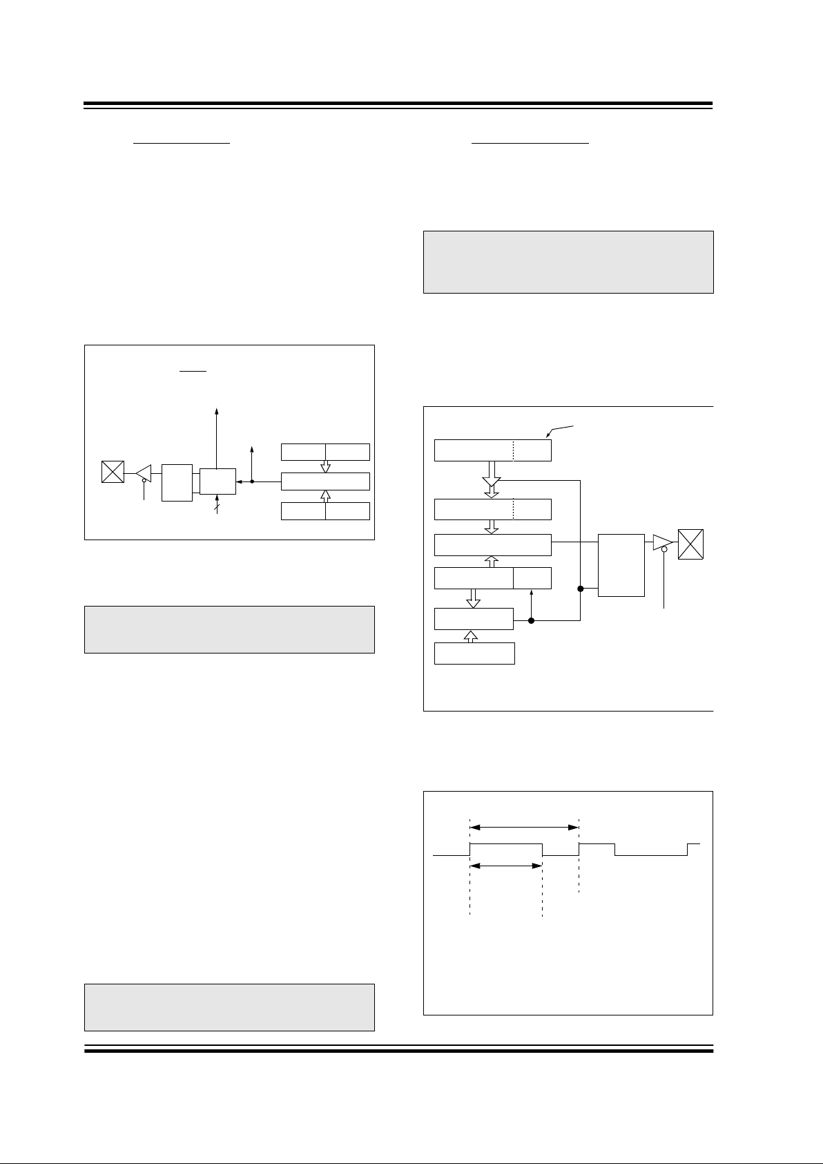
PIC16C745/765
DS41124A-page 54 Advanced Information
1999 Microchip Technology Inc.
9.2 Compare Mode
In Compare mode, the 16-bit CCPR1 register value is
constantly compared against the TMR1 register pair
value. When a match occurs, the RC2/CCP1 pi n is:
• Driven high
•Driven low
• Remains unchanged
The action on the pin is based on the value of control
bits CCP1M<3:0> (CCP1CON<3:0>). At the same
time, interrupt flag bit CCP1IF is set.
FIGURE 9-2: COMPARE MODE OPERATION
BLOCK DIAGRAM
9.2.1 CCP PIN CONFIGURATION
The user must configure the RC2/CCP1 pin as an out-
put by clearing the TRISC<2> bit.
9.2.2 TIMER1 MODE SELECTION
Timer1 must be running in Timer mode or Synchro-
nized Counter mode if the CCP module is using the
compare feature. In Asynchronous Counter mode, the
compare operation may not work.
9.2.3 SOFTWARE INTERRUPT MODE
When Generate Softw are Interrupt mode is c hosen, the
CCP1 pin is not affected. The CCPIF bit is set causing
a CCP interrupt (if enabled).
9.2.4 SPECIAL EVENT TRIGGER
In this mode, an i nternal hardw a re trigger is g ener ated,
which may be used to initiate an action.
The special event trigger output of CCP1 resets the TMR1
register pair. This allows the CCPR1 register to effectively
be a 16-bit programmable period register for Timer1.
The special event trigger output of CCP2 resets the
TMR1 register pair and st arts an A/D co nversion (if the
A/D module is enabled).
9.3 PWM Mode (PWM)
In pulse width modulation mode, the CCPx pin produces up to a 10-bit reso lution PWM output. Since the
CCP1 pin is multiple xe d with the PORTC data latch, the
TRISC<2> bit must be cleared to make the CCP1 pin
an output.
Figure 9-3 shows a simp lified bloc k diagr am of the CCP
module in PWM mode.
For a step b y st ep pro cedure on ho w to set up the CCP
module for PWM operation, see Section 9.3.3.
FIGURE 9-3: SIMPLIFIED PWM BLOCK
DIAGRAM
A PWM output (Fig ure9-4) has a time ba se ( period) and
a time that the outpu t stays high (duty cycle). The frequency of the PWM is the inverse of the period (1/period).
FIGURE 9-4: PWM OUTPUT
Note: Clearing the CCP1CON register will force
the RC2/CCP1 compare output lat ch to the
default low level. This is not the data latch.
Note: The special event trigger from the
CCP1and CCP2 modul es will not se t interrupt flag bit TMR1IF (PIR1<0>).
CCPR1H CCPR1L
TMR1H TMR1L
Comparator
QS
R
Output
Logic
Special Event Trigger
Set flag bit CCP1IF
(PIR1<2>)
match
RC2/CCP1
TRISC<2>
CCP1CON<3:0>
Mode Select
Output Enable
Pin
Special event trigger will:
reset Timer1, but not set interrupt flag bit TMR1IF (PIR1<0>),
and set bit GO/DONE
(ADCON0<2>).
Note: Clear ing the CCP1CON re gister wi ll force
the CCP1 PWM output latch to the default
low level. This is not the PORTC I/O data
latch.
CCPR1L
CCPR1H (Slave)
Comparator
TMR2
Comparator
PR2
(Note 1)
R
Q
S
Duty Cycle Registers
CCP1CON<5:4>
Clear Timer,
CCP1 pin and
latch D.C.
TRISC
<2>
RC2/CCP1
Note 1: 8-bit timer is concatenated with 2-bit internal Q clock
or 2 bits of the prescaler to create 10-bit time-base.
Period
Duty Cycle
(1)
(1)
Note 1: At this time, the TMR2 register is equal to the PR2 register.
CCP1
(2)
2: Output signal is shown as asserted high.

1999 Microchip Technology Inc.
Advanced Information DS41124A-page 55
PIC16C745/765
9.3.1 PWM PERIOD
The PWM period is specified by writing to the PR2 register. The PWM period can be calculated using the following formula:
PWM period = [(PR2) + 1] • 4 • T
OSC •
(TMR2 prescale value)
PWM frequency is defined as 1 / [PWM period].
When TMR2 is equal to PR2, th e follo wing three e v ents
occur on the next increment cycle:
• TMR2 is cleared
• The CCP1 pin is set (exception: if PWM duty
cycle = 0%, the CCP1 pin will not be set)
• The PWM duty cycle is latched from CCPR1L into
CCPR1H
9.3.2 PWM DUTY CYCLE
The PWM duty cycle is specified by writing to the
CCPR1L register and to the CCP1CON<5:4> bits. Up
to 10-bit res olu tio n is available. Th e CCPR 1L co ntai ns
the eight MSbs and the CC P1CON<5: 4> contai ns the
two LSbs. This 10-bit value is represented by
CCPR1L:CCP1CON<5:4>. The following equation is
used to calculate the PWM duty cycle in time:
PWM duty cycle = (CCPR1L:CCP1CON<5:4>) •
Tosc • (TMR2 prescale value)
CCPR1L and CCP1CO N<5:4> c an be writ ten to a t an y
time, but the duty cycle value is not latched into
CCPR1H until af ter a match bet ween PR2 and TMR 2
occurs (i.e., the period is complete). In PWM mode,
CCPR1H is a read-only register.
The CCPR1H register and a 2-bit internal latch are
used to double buffer the PWM duty cycle. This dou b l e
buffering is essential for glitchless PWM operation.
When the CCPR1H and 2-bit latch match TMR2 concatenated with an internal 2-bit Q clock or 2 bits of the
TMR2 prescaler, the CCP1 pin is cleared.
Maximum PWM resolution (bits) for a given PWM
frequency:
9.3.3 SET-UP FOR PWM OPERATION
The following step s should be ta ken when co nfigur ing
the CCP module for PWM operation:
1. Set the PWM period by writing to the PR2 register.
2. Set the PWM duty cycle by writing to the
CCPR1L register and CCP1CON<5:4> bits.
3. Make the CCP1 pin an outp ut by clearing the
TRISC<2> bit.
4. Set the TM R2 prescale v alue and enab le Timer2
by writing to T2CON.
5. Con figure the CC P1 module f or PWM o peratio n.
Note: The Timer2 postscaler (see Se cti on8.1) is
not used in th e deter mi nati on of the PWM
frequency. The postscaler could be used to
have a servo update rate at a different frequency than the PWM output.
Note: If the PWM duty cycle value is longer than
the PWM period, the CCP1 pin will not be
cleared.
log(
FPWM
log(2)
F
INT
)
bits
=
Resolution

PIC16C745/765
DS41124A-page 56 Advanced Information
1999 Microchip Technology Inc.
TABLE 9-3: REGISTERS ASSOCIATED WITH CAPTURE, COMPARE, AND TIMER1
TABLE 9-4: REGISTERS ASSOCIATED WITH PWM AND TIMER2
Address Name Bit 7 Bit 6 Bit 5 Bit 4 Bit 3 Bit 2 Bit 1 Bit 0
Val ue on:
POR,
BOR
Val ue on
all othe r
resets
0Bh,8Bh,
10Bh,18Bh
INTCON GIE PEIE T0IE INTE RBIE T0IF INTF RBIF 0000 000x 0000 000u
0Ch PIR1
PSPIF
(1)
ADIF RCIF TXIF USBIF CCP1IF TMR2IF TMR1IF 0000 0000 0000 0000
0Dh PIR2
— — — — — — —CCP2IF---- ---0 ---- ---0
8Ch PIE1
PSPIE
(1)
ADIE RCIE TXIE USBIE CCP1IE TMR2IE TMR1IE 0000 0000 0000 0000
8Dh PIE2
— — — — — — —CCP2IE---- ---0 ---- ---0
87h TRISC PORTC Data Direction Register 1111 1111 1111 1111
0Eh TMR1L Holding register for the Least Significant Byte of th e 16-bit TMR 1 register xxxx xxxx uuuu uuuu
0Fh TMR1H Holding register for the Most Significan t Byte o f the 16-bit T MR 1 register xxxx xxxx uuuu uuuu
10h T1CON
— — T1CKPS1 T1CKPS0 T1OSCEN T1SYNC TMR1CS TMR1ON --00 0000 --uu uuuu
15h CCPR1L Capture/Compare/PWM register1 (LSB) xxxx xxxx uuuu uuuu
16h CCPR1H Capture/Compare/PWM register1 (MSB) xxxx xxxx uuuu uuuu
17h CCP1CON
— — DCnB1 DCnB0 CCP1M3 CCP1M2 CCP1M1 CCP1M0 --00 0000 --00 0000
1Bh CCPR2L Capture/Compare/PWM register2 (LSB) xxxx xxxx uuuu uuuu
1Ch CCPR2H Capture/Compare/PWM register2 (MSB) xxxx xxxx uuuu uuuu
1Dh CCP2CON
— — DCnB1 DCnB0 CCP2M3 CCP2M2 CCP2M1 CCP2M0 --00 0000 --00 0000
Legend: x = unknown, u = unchanged, - = unimplemented read as ’0’. Shaded cells are not used by Capture and Timer1.
Note 1: The PSP is not implemented on the PIC16C745; always maintain these bits clear.
Address Name Bit 7 Bit 6 Bit 5 Bit 4 Bit 3 Bit 2 Bit 1 Bit 0
Value on:
POR,
BOR
Value on
all other
resets
0Bh,8Bh,
10Bh,18B h
INTCON GIE PEIE
T0IE INTE RBIE T0IF INTF RBIF
0000 000x 0000 000u
0Ch PIR1 PSPIF
(1)
ADIF RCIF TXIF USBIF CCP1IF TMR2IF TMR1IF
0000 0000 0000 0000
0Dh PIR2 — — — — — — — CCP2IF
---- ---0 ---- ---0
8Ch PIE1 PSPIE
(1)
ADIE RCIE TXIE USBIE CCP1IE TMR2IE TMR1IE
0000 0000 0000 0000
8Dh PIE2 — — — — — — — CCP2IE
---- ---0 ---- ---0
87h TRISC PORTC Data Direction Regi ster 1111 1111 1111 1111
11h TMR2 Timer2 module’s regist er
0000 0000 0000 0000
92h PR2 Timer2 module’s period register
1111 1111 1111 1111
12h T2CON — TOUTPS3 TOUTPS2 TOUTPS1 TOUTPS0 TMR2ON T2CKPS1 T2CKPS0
-000 0000 -000 0000
15h CCPR1L Capture/Compare/PWM register1 (LSB)
xxxx xxxx uuuu uuuu
16h CCPR1H Capture/Co mpare/PWM registe r1 (MSB)
xxxx xxxx uuuu uuuu
17h CCP1CON — —
DCnB1 DCnB0
CCP1M3 CCP1M2 CCP1M1 CCP1M0
--00 0000 --00 0000
1Bh CCPR2L Capture/Compare/PWM register2 (LSB)
xxxx xxxx uuuu uuuu
1Ch CCPR2H Capture/Compare/PWM register2 (MSB)
xxxx xxxx uuuu uuuu
1Dh CCP2CON — —
DCnB1 DCnB0
CCP2M3 CCP2M2 CCP2M1 CCP2M0
--00 0000 --00 0000
Legend: x = unknown, u = unchanged, - = unimplemented read as '0'. Shaded cells are not used by PWM and Timer2.
Note 1: Bits PSPIE and PSPIF are reserved on the PIC16C745; always maintain these bits clear.

1999 Microchip Technology Inc.
Advanced Information DS41124A-page 57
PIC16C745/765
10.0 UNIVERSAL SERIAL BUS
10.1 Overview
This section introduces a minimum amount of information on USB. If you already have basic knowledge of
USB, you can safely skip this section. If terms like
Enumeration, Endpoint, IN/OUT Transactions, Transfers and Low Speed/Full Speed are foreign to you,
read on.
USB was developed to address the increased connec-
tivity needs of PC’s in the PC 2000 specification.
There was a base requirement to increase the bandwidth and number of de v ices , whic h cou ld be a ttache d.
Also desired were the ability for hot swapping, user
friendly operation, robust communications and low
cost. The primary promoters of USB are Intel, Compaq, Microsoft and NEC.
USB is implemented as a Tiered Star topology, with
the host at the top, hubs in the middle, spreading out
to the individual devices at the end. USB is limited to
127 devices on the bus, and the tree cannot be more
than 6 levels deep.
USB is a host centric architecture. The host is always
the master. Devices are not allowed to “speak” unless
“spoken to” by the host.
Transfers take place at one of two speeds. Full Speed
is 12 Mb/s and Low Speed is 1.5 Mb/s. Full Speed
covers the middle ground of data intensive audio and
compressed video applications, while low speed supports less data intensive applications.
10.1.1 TRANSFER PROTOCOLS
Four transfer protocols are defined, each with
attributes:
- Isochronous Transfers, meaning equal time,
guarantee a fixed amount of data at a fixed
rate. This mode trades off guaranteed data
accuracy for guaranteed timeliness. Data
validity is no t checked because t here isn’t
time to re-send bad packets anyway and the
consequences of bad data are not catastrophic.
- Bulk Transfers are the converse of Isochonous. Data accuracy is guaranteed, but timeliness is not.
- Interrupt Transfers are designed to communicate with devices which have a moderate
data rate requirement. Human Interface
Devices like keyboards are but one example.
For Interrupt Transfers, the key is the desire
to transfer data at regular intervals. USB periodically polls thes e devices at a fixed rate to
see if there is data to transfer.
- Control Transfers are used for configuration
purposes.
10.1.2 FRAMES
Information communicated on the bus is grouped in a
format called Frames. Each Frame is 1 ms in duration
and is composed of multiple transfers. Each transfer
type can be repeated more than once within a frame.
10.1.3 POWER
Power has always been a concern with any device.
With USB, 5 volt power is now available directly from
the bus. Devices may be self-powered or bus-powered. Self-powered devices will draw power from a
wall adapter or power brick. On the other hand, buspowered devices will draw power directly from the
USB bus itself. There are limits to how much power
can be drawn from the USB bus. Power is expressed
in terms of “unit loads” (≤100 mA). All devices, including Hubs, are guaranteed at least 1 unit load (low
power), but must negotiate with the host for up to 5
unit loads (high power). If the host determines that the
bus as currently configured cannot support a device’s
request for more unit loads, the device will be denied
the extra unit loads and must remain in a low power
configuration.
10.1.4 END POINTS
At the lowest level, each device controls one or more
endpoints. An endpoint can be thought of as a virtual
port. Endpoints are used to communicate with a
device’s functions. Each endpo in t i s a so u r ce o r s ink of
data. Endpoints have both an In and Out direction
associated with it. Each device must implement endpoint 0 to support Control Transfers for configuration.
There are a maximum of 15 endpoints available for
use by each full speed device and 6 endpoints for
each slow speed device. Remember that the bus is
host centric, so In/Out is with respect to the host and
not the device.
10.1.5 ENUMERATION
Prior to communicating on the bus, the host must see
that a new device has been connected and then go
through an “enumeration process”. This process
allows the host to ask the device to introduce itself,
and negotiate performance parameters, such as
power consumption, transfer protocol and polling rate.
The enumeration process is initiated by the host when
it detects that a new device has attached itself to the
bus. This takes place completely in the background
from the application process.
10.1.6 DESCRIPTORS
The USB specification requires a number of di fferent
descriptors to provide information necessary to identify a devi ce , spec ify it s endp oints , and ea ch end point’s
function. The fiv e general categories of descriptors are
Device, Configuration, Interface, End Point and String.

PIC16C745/765
DS41124A-page 58 Advanced Information
1999 Microchip Technology Inc.
The Device descriptor provides general information
such as manufacture r, product num ber, seria l num ber,
USB device cla ss the p rodu ct f al ls un der, and the number of different configurations supported. There can
only be one Device descriptor for any given application.
The Configuration descriptor provides information on
the power requirements of the device and how many
different interfaces are supported when in this configuration. There may be more than one configuration for
each device, (i.e., a hig h power device may also support a low power configuration).
The Interface descriptor details the number of endpoints used in this interface, as well as the class driver
to use should the device support functions in more
than just one device class. There can only be one
Interface descriptor for each co nfiguration.
The Endpoint descriptor details the actual registers for
a given function. Information is stored about the transfer types supported, direction (In/Out), bandwidth
requirements and polling inter val. There may be more
than one endpoint in a device, and endpoints may be
shared between different interfaces.
Many of the four descriptors listed above will reference
or index different Str ing descriptors. String descriptors
are used to provide vendor specific or application specific information. They may be optional and are
encoded in “Unicode” format.
10.1.7 DEVICE CLASSES/CLASS DRIVERS
Operating systems provide drivers which group func-
tions together by common device types called classes.
Examples of device classes include, but are not limited
to, storage, audio, communications and HID (H um an
Interface). Class drivers for a given application are referenced in both the Device descriptor and Interface
descriptor. Most applications can find a Class Driver
which supports the majority of their function/command
needs. Vendors who have a requirement for specific
commands which are not supported by any of the
standard class drivers may provide a vendor specific
“.inf” file or driver for extra support.
10.1.8 SUMMARY
While a complete USB over view is beyond the scope
of this document, a few key concepts must be noted.
Low speed communication is designed for devices,
which in the past, used an interrupt to communicate
with the host. In the USB scheme, devices do not
directly interrupt the processor when they have data.
Instead the host perio dic al ly poll s e ach device to see if
they have any data. This polling rate is negotiated
between the device and host, giving the system a
guaranteed latency.
For more details on USB, see the USB V1.1 spec,
available from the USB website at www.usb.org.
10.2 Application Isolation
Microchip provides a comprehensive support library of
standard chapter 9 USB commands. These libraries
provide a software layer to insulate the application
software from having to handle the complexities of the
USB protocol. A simple Put/Get interface is implemented to allow most of the USB processing to take
place in the background within the USB interrupt service routine. Applications are encouraged to use the
provided librar ies during both enumeration and configured operation.
10.3 Introduction
The USB peripheral module supports Low Speed control and interrupt (IN and OUT) transfers. The implementation supports 3 endpoint numbers (0, 1, 2) for a
total of 6 endpoints.
The following terms are used in the description of the
USB module:
• MCU - The core processor and corresponding
firmware
• SIE - Serial Interface Engine: That part of the
USB that performs functions such as CRC generation and clocking of the D+ and D- signals.
• USB - The USB module including SIE and registers
• Bit Stuffing - forces insertion of a transition on D+
and D- to maintain clock synchronization
• BD - Buffer Descriptor
• BDT - Buffer Descriptor Table
• EP - Endpoint (combination of endpoint number
and direction)
• IN - Packet transfer into the host
• OUT - Packet transfer out of the host
10.4 USB Transaction
When the USB transmits or receives data the SIE will
first check that the corresponding endpoint and direction Buffer Description UOWN bit equals 1. The USB
will move the data to or from the corresponding buffer.
When the TOKEN is comp lete , the USB will update th e
BD status and change the UOWN bit to 0. The USTAT
register is updated and the TOK_DNE interrupt is set.
When the MCU processes the TOK_DNE interrupt it
reads the USTAT register, which gives the MCU the
information it needs to process the endpoint. At this
point the MCU will process the data and set the corresponding UOWN bit. Figure 10-1 shows a time line of
how a typical USB token would be processed.

1999 Microchip Technology Inc.
Advanced Information DS41124A-page 59
PIC16C745/765
FIGURE 10-1: USB TOKENS
USB RESET
ACKSETUP TOKEN DA TA
USB_RST
Interrupt Generated
TOK_DNE
Interrupt Generated
ACKIN TOKEN DATA
TOK_DNE
Interrupt Generated
ACKOUT TOKEN DA TA
TOK_DNE
Interrupt Generated
= Host
= Device

PIC16C745/765
DS41124A-page 60 Advanced Information
1999 Microchip Technology Inc.
10.5 US B Register Map
The USB Control Registers, Buffer Descriptors and
Buffers are located in Bank 3.
10.5.1 CONTROL AND STATUS REGISTERS
The USB module is controlled by 7 registers, plus
those that control each endpoint and endpoint/direction buffer.
10.5.1.1 USB Interrupt Register (UIR)
The USB Interrupt Status Register (UIR) contains flag
bits for each of the interrupt sources within the USB.
Each of these bits are qualified with their respective
interrupt enable bits (see the Interrupt Enable Register
UIE). All bits of the register are logically OR’ed
together to f orm a si ngl e i nterrupt source for the microprocessor interrupt found in PIR1 (USBIF). Once an
interrup t bit has been set, it must be cleared by writing
a 0.
REGISTER 10-1: USB INTERRUPT FLAGS REGISTER (UIR: 190h)
U-0 U-0 R/C-0 R/C-0 R/C-0 R/C-0 R/C-0 R/C-0
— — STALL UIDLE TOK_DNE ACTIVITY UERR USB_RST R = Rea dable bit
C = Clearable bit
U = Unimplemented bit,
read as ‘0’
-n = Value at POR reset
bit7 bit0
bit 7-6: Unimplemented: Read as '0'.
bit 5: STALL: A STALL handshake was sent by the SIE.
bit 4: UIDLE: This bit is set if the USB has detected a constant idle on the USB bus signals for 3 ms. The idle
timer is reset by activity on the USB bus. Once a IDLE condition has been detected, the user may wish
to place the USB module in SUSPEND by setting the SUSPEND bit in the UCTRL register.
bit 3: T O K_DNE: This bit is set when the current token being processed is complete. The microprocessor
should immediately read the USTAT register to determine the Endpoint number and direction used for
this token. Clearing this bit causes the USTAT register to be cleared or the USTAT holding register to be
loaded into the STAT register if another token has been processed.
bit 2: ACTIVITY: Activity on the D+/D- lines will cause the SIE to set this bit. Typically this bit is unmasked
following detection of SLEEP. Users must enable the activity interrupt in the USB Interrupt Register
(UIE: 191h) prior to entering suspend.
bit 1: UERR: This bit is set when any of the error conditions within the ERR_STAT register has occurred. The
MCU must then read the ERR_STAT register to determine the source of the error.
bit 0: USB_RST: Thi s bit is set when the USB has decod ed a valid USB reset. This wil l inform the MCU to write
00h into the address register and enable endpoint 0. USB_RST is set once a USB reset has been
detected for 2.5 microseconds. It will not be asserted again until the USB reset condition has been
removed, and then reasserted.
Note1: Bits can only be modified when UCTRL.SUSPND = 0.

1999 Microchip Technology Inc.
Advanced Information DS41124A-page 61
PIC16C745/765
10.5.1.2 USB Interrupt Enable Register (UIE)
The USB Interrupt Enable Register (UIE) contains
enable bits for each of the interrupt sources within the
USB. Setting any of t hese bits w ill enable the respective interrupt source in the UIR register. The values in
the UIE register only affect the propagation of an interrupt condition to the PIE1 register. Interrupt conditions
can still be polled and serviced.
REGISTER 10-2: USB INTERRUPT ENABLE REGISTER (UIE: 191h)
U-0 U-0 R/W-0 R/W-0 R/W-0 R/W-0 R/W-0 R/W-0
— — STALL UIDLE TOK_DNE ACTIVITY UERR USB_ RST R = Readable bit
W = Writable bit
U = Unimplemented bit,
read as ‘0’
-n = Value at POR reset
bit7 bit0
bit 7-6: Unimplemented: Read as '0'.
bit 5: ST ALL: Set to enable STALL interrupts.
1 = STALL interrupt enabled
0 = STALL interrupt disabled
bit 4: UIDLE: Set to enable IDLE interrupts.
1 = IDLE interrupt enabled
0 = IDLE interrupt disabled
bit 3: TOK_DNE: Set to enable TOK_DNE interrupts.
1 = TOK_DNE interrupt enabled
0 = TOK_DNE interrupt disabled
bit 2
(1)
: ACTIVITY: Set to enable ACTIVITY interrupts.
1 = ACTIVITY interrupt enabled
0 = ACTIVITY interrupt disabled
bit 1: UERR: Set to enable ERROR interrupts.
1 = ERROR interrupt enabled
0 = ERROR interrupt disabled
bit 0: USB_RST : Set to enable USB_RST interrupts.
1 = USB_RST interrupt enabled
0 = USB_RST interrupt di sabled
Note 1: This interrupt is the only interrupt active during UCTRL suspend = 1.

PIC16C745/765
DS41124A-page 62 Advanced Information
1999 Microchip Technology Inc.
10.5.1.3 USB Error Interrupt Status Register (UEIR)
The USB Error Interrupt Status Register (UEIR) con-
tains bits for each of the error sources within the USB.
Each of these bits are enab le d b y their respe ctiv e error
enable bits (UEIE). The result is OR’ed together and
sent to the ERROR bi t of the UIR register. Once an
interrupt bit has been set it must be cleared by writing
a zero to the respective interr upt bit. Each bit is set as
soon as the error condition is de tected . Thus, th e interrupt will typically not correspond with the end of a
token being processe d.
REGISTER 10-3: USB ERROR INTERRUPT FLAGS STATUS REGISTER (UEIR: 192h)
R/C-0 R/C-0 R/C-0 R/C-0 R/C-0 R/C-0 R/C-0 R/C-0
BTS_ERR OWN_ERR WRT_ERR BTO_ERR DFN8 CRC16 CRC5 PID_ERR R = Readable bit
C = Clearable bit
U = Unimplemented
bit, read as ‘0’
-n = Value at POR
reset
bit7 bit0
bit 7: BTS_ERR: A bit stuff error has been detected.
bit 6: OWN_ERR: This bit is set if the USB is processing a token and the OWN bit within the BD T is equal to 0
(signifying that the micro processor owns the BDT an d the SIE does not ha v e acce ss to the BDT). If processing an IN TOKEN this would cause a transmit data und erflow condition. Pr ocessing an OUT o r SETUP
TOKEN would cause a receive data overflow condition.
bit 5: WRT_ERR: Write Error. A write by the MCU to the USB Buffer Descriptor Table or Buffer area was unsuc-
cessful.
bit 4: BTO_ERR: This bit is set if a bus turnaround time-out error has occurred. This USB uses a bus turnaround
timer to keep track of the amount of time elapsed between the token and data phases of a SETUP or OUT
TOKEN or the data and handshake phases of a IN TOKEN. If more than 17-bit times are counted from the
previous EOP before a transition from IDLE, a bus turnaround time-out error will occur.
bit 3: DFN8: The data field received was not 8 bits. The USB Specific ation 1 .1 specifi es tha t data fie ld m ust be a n
integral number of bytes. If the data field was not an integral number of bytes this bit will be set.
bit 2: CRC16: The CRC16 failed.
bit 1: CRC5: This interrupt will detect CRC5 error in the token packets generated by the host. If set the token
packet was rejected due to a CRC5 error.
bit 0: PID_ERR: The PID check field failed.
Note1: Bits can only be modified when UCTRL.SUSPND = 0.

1999 Microchip Technology Inc.
Advanced Information DS41124A-page 63
PIC16C745/765
10.5.1.4 Error Interrupt Enable Register (UEIE)
The USB Error Interrupt Enable Register (UEIE) con-
tains enable bits for each of the error interrupt sources
within the USB. Setting any of these bits will enable
the respective error interrupt source in the UEIR register.
REGISTER 10-4: USB ERROR INTERRUPT ENABLE REGISTER (UEIE: 193h)
R/W-0 R/W-0 R/W-0 R/W-0 R/W-0 R/W-0 R/W-0 R/W-0
BTS_ERR OWN_ERR WRT_ERR BTO_ERR DFN8 CRC16 CRC5 PID_ERR
R = Readable bit
W = Writable bit
U = Unimplemented bit,
read as ‘0’
-n = Value at POR reset
bit7 bit0
bit 7: BTS_ERR: Set this bit to enable BTS_ERR interrupts.
1 = BTS_ERR interrupt enabled
0 = BTS_ERR interrupt disabled
bit 6: OWN_ERR: Set this bit to enable OWN_ERR interrupts.
1 = OWN_ERR interrupt enabled
0 = OWN_ERR interrupt disabled
bit 5: WRT_ERR: Set this bit to enable WRT_ERR interrupts.
1 = WRT_ERR interrupt enabled
0 = WRT_ERR interrupt disabled
bit 4: BTO_ERR: Set this bit to enable BTO_ERR interrupts.
1 = BTO_ERR interrupt enabled
0 = BTO_ERR interrupt disabled
bit 3: DFN8: Set this bit to enable DFN8 interrupts.
1 = DFN8 interrupt enabled
0 = DFN8 interrupt disabled
bit 2: CRC16: Set this bit to enable CRC16 interrupts.
1 = CRC16 interrupt enabled
0 = CRC16 interrupt disabled
bit 1: CRC5: Set this bit to enable CRC5 interrupts.
1 = CRC5 interrupt enabled
0 = CRC5 interrupt disabled
bit 0: PID_ERR: Set this bit to enable PID_ERR interrupts.
1 = PID_ERR interrupt enabled
0 = PID_ERR interrupt disabled

PIC16C745/765
DS41124A-page 64 Advanced Information
1999 Microchip Technology Inc.
10.5.1.5 St atus Register (USTAT)
The USB Status Register reports the transaction sta-
tus within the USB. When the MCU recognizes a
TOK_DNE interrupt, this register should be read to
determine the status of the previous endpoint communication. The data in the status register is valid when
the TOK_DNE interrupt bit is asserted.
The USTAT register is actually a read window into a
status FIFO maintained by the USB. When the USB
uses a BD, it updates the status register. If another
USB transaction is performed before the TOK_DNE
interrupt is serviced the USB will store the sta tus of the
next transac tion in the STAT FIFO. Thus , the STAT register is actually a four byte FIFO which allo ws the MC U
to process one transaction while the SIE is processing
the next. Clearing the TOK_DNE bit in the INT_STAT
register causes the SIE to update the STAT register
with the contents of the next STAT value. If the data in
the STAT holding register is valid, the SIE will immediately reassert the TOK_DNE interrupt.
REGISTER 10-5: USB STATUS REGISTER (USTAT: 194h)
U-0 U-0 U-0 R-X R-X R-X U-0 U-0
— — —
ENDP1 ENDP0 IN
— — R = Readable bit
W = Writable bit
U = Unimplemented bit ,
read as ‘0’
-n = Value at POR reset
X = Don’t care
bit7 bit0
bit 7-5: Unimplemented: Read as ’0’.
bit 4-3: ENDP<1:0>: These bits encode the endpoint address that received or transmitted the previous token.
This allows the mi croprocessor to determine which BDT entry was updated by the last USB transaction.
bit 2: IN: This bit indicates the direction of the last BD that was updated.
1 = The last transaction was an IN TOKEN
0 = The last transaction was an OUT or SETUP TOKEN
bit 1-0: Unimplemented: Read as ’0’.

1999 Microchip Technology Inc.
Advanced Information DS41124A-page 65
PIC16C745/765
10.5.1.6 USB Control Register (UCTRL)
The control register provides various control and con-
figuration inform ation for the USB.
REGISTER 10-6: USB CONTROL REGISTER (UCTRL: 195h)
U-0 U-0 R-X R/C-0 R/W-0 R/W-0 R/W-0 U-0
— —
SE0 PKT_DIS Config_Bit RESUME SUSPND
— R = Readable bit
W = Writable bit
C = Clearable bit
U = Unimplemented bit,
read as ‘0’
-n = Value at POR reset
X = Don’t care
bit7 bit0
bit 7-6: Unimplemented: Read as ’0’.
bit 5: SE0: Live Single Ended Zero. This status bit indicates that the D+ and D- lines are both pulled to low.
1 = single ended zero being received
0 = single ended zero not being received
bit 4 PKT_DIS: The PKT_DIS bit informs the MCU that the SIE has disabled packet transmission and recep-
tion. Clearing this bit all o ws the SIE to continue token processing. This bit is se t by the SIE when a Setup
Token is received a llowing s oftware to deq ueue any pending pac ket t ransactio ns in the BDT bef ore resu ming token processing. The PKT_DIS bit is set under certain conditions such as back to back SETUP
tokens. This bit is not set on every SETUP token and can be modified only when UCTRL.SUSPND = 0.
bit 3: Config_Bit: Configuration bit used by firmware during e numeration.
bit 2: RESUME: Setting this bit will allow the USB to execute resume signaling. This will allow the USB to per-
form remote wake-up. Software must set RESUME to 1 for 10 mS then clear i t to 0 to ena ble remote wake-
up. For more information on RESUME signaling, see Section 7.1.7.5, 11.9 and 11.4.4 in the USB 1.1 spec-
ification.
1 = perform Resume signaling
0 = normal operation
bit 1: SUSPND: Suspends USB operation and clocks and places the module in low power mode. This bit will
generally be set in response to a UIDLE interrupt. It will generally be reset after an ACTIVITY interrupt.
The V
USB pin will still be driven, however the transceiver outputs are disabled.
1 = USB module in power conserve mode
0 = USB module normal operation
bit 0: Unimplemented: Read as ’0’.

PIC16C745/765
DS41124A-page 66 Advanced Information
1999 Microchip Technology Inc.
10.5.1.7 USB Address Register (UADDR)
The Address Register (UADDR) contains the unique
USB address that the USB will decode. The register is
reset to 00h after the reset inp ut has go ne acti v e or the
USB has decoded a USB reset signaling. That will initialize the address register to decode address 00h as
required by the USB specification. The USB address
must be wri tten by the MCU du ring the US B SETUP
phase.
REGISTER 10-7: USB ADDRESS REGISTER (UADDR: 196h)
10.5.1.8 USB Software Status Register
This register is used by the USB firmware libraries for
USB status.
REGISTER 10-8: RESERVED SOFTWARE LIBRARY REGISTER (USWSTAT: 197H):.
10.5.1.9 Endpoint Registers
Each endpoint is controlled by an Endpoint Control
Register. The PIC16C745/765 supports Buffer
Descriptors (BD) for the following endpoints:
- EP0 Out
- EP0 In
- EP1 Out
- EP1 In
- EP2 Out
- EP2 In
The user will be required to disable unused Endpoints
and directions using the Endpoint Control Registers.
U-0 R/W-0 R/W-0 R/W-0 R/W-0 R/W-0 R/W-0 R/W-0
—
ADDR6 ADDR5 ADDR4 ADDR3 ADDR2 ADDR1 ADDR0
R = Readable bit
W = Writable bit
U = Unimplemented bit,
read as ‘0’
-n = Value at POR reset
bit7 bit0
bit 7: Unimplemented : Read as ’0’.
bit 6-0: ADDR<6:0>: This 7-bit value defines the USB address that the USB will decode.
R/W-0 R/W-0 R/W-0 R/W-0 R/W-0 R/W-0 R/W-0 R/W-0 R = Readable bit
W = Writable bit
U = Unimplemented bit,
read as ‘0’
-n = Value at POR reset
7
65 432 1 0
Function IDs Configuration Status

1999 Microchip Technology Inc.
Advanced Information DS41124A-page 67
PIC16C745/765
10.5.1.10 USB Endpoint Control Register (EPCn)
The Endpoint Control Registers contains the endpoint
control bits for each of the 6 endpoints available on
USB for a decoded address. These four bits define the
control necessary for any one endpoint. Endpoint 0
(ENDP0) is associated with control pipe 0 which is
required by USB for all functions (IN, OUT, and
SETUP). Therefore, after a USB_RST interrupt has
been received the microprocessor should set ENDPT0
to contain 06h.
REGISTER 10-9: USB ENDPOINT CONTROL REGISTER (UEPn: 198H-19Ah)
U-0 U-0 U-0 U-0 R/W-0 R/W-0 R/W-0 R/W-0
— — — —
EP_CTL_DIS EP_OUT_EN EP_IN_EN EP_STALL
R = Readable bit
W = Writable bit
U = Unimplemented bit,
read as ‘0’
-n = Value at POR reset
bit7 bit0
bit 7-4: Unimplemented: Read as ’0’.
bit 3-1: EP_CTL_DIS, EP_OUT_EN, EP_IN_EN: These three bits define if an endpoint is enabled and the direc-
tion of the endpoint. The endpoint enable/direction control is defined as follows:
bit 0: EP_STALL: When this bit is set it indicates that the endpoint is stalled. This bit has priority over all other
control bits in the Endpo int Enable re gister , but is on ly valid if EP_I N_EN=1 or EP_OUT_EN=1. A ny access
to this endpoint will cau se the USB to retu rn a STALL handshake . The EP_STALL bit can be se t or cleared
by the SIE. Refer to the USB 1.1 Specification, Sections 4.4.4 and 8.5.2 for more details on the STALL
protocol.
EP_CTL_DIS EP_OUT_EN EP_IN_EN Endpoint Enable/Direction Control
X 0 0 Disable Endp oi nt
X 0 1 Enable Endpoint for IN tokens only
X 1 0 Enable Endpoint for OUT tokens only
1 1 1 Enable Endpoint for IN and OUT tokens
0 1 1 Enable Endpoint for IN, OUT, and SETUP tokens

PIC16C745/765
DS41124A-page 68 Advanced Information
1999 Microchip Technology Inc.
10.6 Buffer Descriptor Table (BDT)
To efficiently manage USB endpoint communications
the USB implements a Buffer Descriptor Table (BDT)
in register space. Every endpoint requires a 4 byte
Buffer Descriptor (BD) entry. Because the buffers are
shared between the MCU and the USB, a simple
semaphore mechanism is used to distinguish which is
allowed to update the BD and buffers in system memory. The UOWN bit is cleared when the BD entry is
“owned” by the MCU. When the UOWN bit is set to 1,
the BD entry and the buffer in system memory is
owned by the USB. The MCU should not modify the
BD or its corresponding data buffer.
The Buffer Descriptors provide endpoint buffer control
information for the USB and MCU. The Buffer Descriptors have different meaning based on the value of the
UOWN bit.
The USB Controller uses the data stored in the BDs
when UOWN = 1 to de termine:
• Data0 or Data1 PID
• Data toggle synchronization enable
• Number of bytes to be transmitted or received
• Starting location of the buffer
The MCU uses the data stored in the BDs when
UOWN = 0 to determine:
• Data0 or Data1 PID
• The received TOKEN PID
• Number of bytes transmitted or received
Each endpoint has a 4 byte Buffer Descriptor and
points to a data buffer in the USB dua l port registe r
space. Control of the BD and buffer would typically be
handled in the following fashion:
• The MCU verifies UOWN = 0, sets the BDndAL to
point to the start of a buffer, if necessary fills the
buffer, then sets the BDndST byte to the desired
value with UOWN = 1.
• When the host commands an in or out transaction, the Serial Interface Engine (SIE) performs
the following:
- Get the buffer address
- Read or write the buffer
- Update the USTAT register
- Update the buffer descriptors with the packet
ID (PID) value
- Set the data 0/1 bit
- Update the byte count
- Clear the UOWN bit
• The MCU is interrupted and reads the USTAT,
translates that value to a BD, where the UOWN,
PID , D ata 0/1 , an d byte count values are chec ked.

1999 Microchip Technology Inc.
Advanced Information DS41124A-page 69
PIC16C745/765
REGISTER 10-10: BUFFER DESCRIPTOR STATUS REGISTER. BITS WRITTEN BY THE MCU
(BDndST: 1A0h, 1A4h, 1A8h, 1ACh, 1B0h, 1B4h)
REGISTER 10-11: BUFFER DESCRIPTOR STATUS. BITS READ BY THE MCU.
(BDndST: 1A0h, 1A4h, 1A8h, 1ACh, 1B0h, 1B4h)
W-X W-X U-X U-X W-X W-X U-X U-X
UOWN DATA0/1 — — DTS BSTALL — — R = Readable bit
W = Writable bit
U = Unimplemented bit,
read as ‘0’
-n = Value at POR reset
X = Don’t care
bit7 bit0
bit 7: UOWN: USB Own. This UOWN bit determ ines who currently owns the buffer. The SIE writes a 0 to this
bit when it has completed a token. This byte of the BD should always be the last byte the MCU updates
when it initializ es a BD. Once the BD has been assig ned t o the USB , the MC U should not c hange it in an y
way .
1 = USB has exclusive access to the BD. The MCU should not modify the BD or buffer.
0 = The MCU has exclusive access to the BD. The USB ignores all other fields in the BD.
bit 6: DA T A0/1: This bit defines the type of data toggle packet that was transmitted or received.
1 = Data 1 packet
0 = Data 0 packet
bit 5-4: Reserved: Read as ’X’.
bit 3: DTS: Setting this b it will e nable the USB to perform Data Toggle Synchronization. If a pack et arrives with
an incorrect DTS, it will be ignored and the buffer will remain unchanged.
1 = Data Toggle Synchronization is performed
0 = No Data Toggle Synchronization is performed
bit 2: BSTALL: Buffer Stall. Setting this bit will cause the USB to issue a STALL handshak e if a token is received
by the SIE that w ould u se the BD i n this loca tion. The BD is no t consumed by the SIE (the o wn bit remains
and the rest of the BD are unchanged) when a BSTALL bit is set.
bit 1-0: Reserved: Read as ’X’.
Note: Recommend that users not use BSF, BCF due to the dual functionality of this register.
R/W-0 R/W-X R/W-X R/W-X R/W-X R/W-X U-X U-X
UOWN DATA0/1 PID3 PID2 PID1 PID0
— — R = Readable bit
W = Writable bit
U = Unimplemented bit,
read as ‘0’
-n = Value at POR reset
X = Don’t care
bit7 bit0
bit 7: UOWN: USB Own. This UOWN bit determines who currently owns the buffer. The SIE writes a 0 to this
bit when it has completed a token. This byte of the BD should always be the last byte the MCU updates
when it initializ es a BD. Once the BD has been assig ned t o the USB , the MC U should not c hange it in an y
way .
1 = USB has exclus ive access to the BD. The MCU should not modify the BD or buffer.
0 = The MCU has exclusive access to the BD. The USB ignores all other fields in the BD.
bit 6: DA T A0/1: This bit defines the type of data toggle packet that was transmitted or received.
1 = Data 1 packet
0 = Data 0 packet
bit 5-2: PID<3:0>: Packet Identifier. The received token PID value
bit 1-0: Reserved: Read as 'X'.
Note: Recommend that users not use BSF, BCF due to the dual functionality of this register.

PIC16C745/765
DS41124A-page 70 Advanced Information
1999 Microchip Technology Inc.
REGISTER 10-12: BUFFER DESCRIPTOR BYTE COUNT (BDndBC: 1A1h, 1A5h, 1A9h, 1ADh, 1B1h,
1B5h))
REGISTER 10-13: BUFFER DESCRIPTOR ADDRESS LOW (BDndAL: 1A2h, 1A6h, 1AAh, 1AEh,
1B2h, 1B6h)
10.6.1 ENDPOINT BUFFERS
Endpoint buffers are located in the Dual Port RAM
area. The starting location of an endpoint buffer is
determined by the Buffer Descriptor.
10.7 TRANSCEIVER
An on-chip integrated transceiver is included to drive
the D+/D- physical layer of the USB.
10.7.1 REGULATOR
A 3.3V regulator provides the D+/D- drives with power.
A +
20% 10nF capacitor is req uir ed on VUSB for regula-
tor stability.
10.7.1.1 VUSB Output
The V
USB provides a 3.3V nominal output. This drive
current is sufficient for a pull-up only.
10.8 USB Software Libraries
Microchip Technology provides a comprehensive set
of Chapter 9 Standard requests functions to aid developers in implementing their designs. See Microchip
Technology’s website for the latest version of the software libraries.
TABLE 10-1: USB PORT FUNCTIONS
U-X U-X U-X U-X R/W-X R/W-X R/W-X R/W-X
— — — — BC3 BC2 BC1 BC0 R = Readable bit
W = Writable bit
U = Unimplemented bit,
read as ‘0’
-n = Value at POR reset
X = Don’t care
bit7 bit0
bit 7-4: Reserved: Read as ’X’.
bit 3-0: BC<3:0>: The Byte Count bits re pres en t th e n u mber o f bytes that will be transmitted for an IN TOKEN or
received during an OUT TOKEN. Valid b yte cou nts are 0 - 8. The SIE wi ll chan ge this fie ld upon the co mpletion of an OUT or SETUP token with the actual byte count of the data received.
R/W-X R/W-X R/W-X R/W-X R/W-X R/W-X R/W-X R/W-X
BA7 BA6 BA5 BA4 BA3 BA2 BA1 BA0 R = Readable bit
W = Writable bit
U = Unimplemented bit,
read as ‘0’
-n = Value at POR reset
X = Don’t care
bit7 bit0
bit 7-0: BA<7:0>: Buff er Addre ss . The base ad dress o f the b uffer controlled by this endpoint. The uppe r orde r bit
address (BA8) of the 9-bit a ddress is assumed to be 1h. Thi s v alue must point t o a location w ithin the du al
port memory space (1B8h - 1DFh). The upper order bits of the address are assumed to point to Bank 3.
Note1: This register should always contain a value between B8h-DFh.
Name Function
Input
Type
Output
Type
Description
V
USB VUSB — Power 3.3V for pull up resistor
D- D- USB USB USB Differential Bus
D+ D+ USB USB USB Differential Bus
Legend: OD = open drain, ST = Schmitt Trigger

1999 Microchip Technology Inc.
Advanced Information DS41124A-page 71
PIC16C745/765
10.9 USB Firmware Users Guide
10.9.1 INTRODUCING THE USB SOFTWARE
INTERFACE
Microchip provid es a layer of software that handles the
lowest level interface so y ou r app lic ati on won’t have to.
This provides a simple Put/Get interface for communication. Mos t of th e USB pr ocessi ng ta kes place in the
background through the Interrupt Service Routine.
From the application viewpoint, the enumeration process and data communication takes place without further interaction.
FIGURE 10-2: USB SOFTWARE INTERFACE
10.9.2 INTEGRATING USB INTO YOUR
APPLICATION
The latest version of the USB interface software is
available on Microchip Technology’s website. See
http://www.microchip.com/
Communicating on USB is similar to communicating
via a hardware USART. The main difference is that a
USART typically works on a single byte at a time,
where USB operates on a buffer of up to 8 bytes at a
time.
There is one function defined to start the enumeration
process and two additional functions are defined for
moving buffers between the main application and the
USB peripheral. InitUSB initializ e s the USB periphera l
allowing the host to enumerate the device. Then for
normal data communications, function PutUSB sends
data to the host and function GetUSB receives data
from the host.
There's a lot that happens behind the scenes to make
the communication work, but these calls are all an
application needs to communicate on the bus. The
rest is handled on an interrupt basis.
InitUSB initializes the Buffer Descriptor table, and
enables the USB interrupt so enumeration can begin.
The actual enumeration process occurs automatically,
driven by the host and interrupt service routine. The
macro ConfiguredUSB waits until the device is in the
CONFIGURED mode and ready to go. The time
required to enumerate is completely dependent on the
host and bus loading.
10.9.3 INTERRUPT STRUCTURE CONCERNS
10.9.3.1 Processor Resources
Most of the USB proc essing occurs via the interr upt
and thus is invisib l e to appli cat ion. How ever it still consumes processor resources. These include ROM,
RAM, Common RAM, Stack Levels and processor
cycles. This section atte mpts to q uantify the impact on
each of these resources, and shows ways to avoid
conflicts.
These are the considerations you'll need to take into
account if you write your own Interrupt Service Routine: Save W, Status, FSR and PCLATH which are the
file registers that may be corrupted by servicing the
USB interrupt.
We provide a skeleton ISR which will do this for you,
and includes tests for each of the possible ISR bits.
This provides a good place to star t from if you haven't
already written your own. See file USB_INT.ASM.
10.9.3.2 Stack Levels
The hardware stack on the device is only 8 levels
deep. So the worst case call between the application
and ISR can only be 8 levels. The enumeration process requires 6 levels, so it's best if the main application holds off on any processing until enumeration is
complete. ConfiguredUSB is a macro that waits until
the enumeratio n process is complete for exactly this
purpose.
10.9.3.3 ROM
The code required to support the USB interrupt,
including the chapte r 9 interface calls, but not inclu ding
the descriptor tables is about 1kW. The descriptor and
string descriptor tables can each take up to an additional 256W. The location of these parts is not
restricted, and the lin k er script may be edited to control
the placement of each part. See the Strings and
Descriptors sections in the linker script
10.9.3.4 RAM
With the exception of Common RAM disc ussed below,
servicing the USB interrupt costs ~40 b y tes of RAM in
Bank 2. That leaves all the General Purpose RAM in
banks zero and one, plus half of bank two available for
your application to use.
10.9.3.5 Common RAM usage
The PIC16C 745/765 has 16 bytes o f common RAM.
These are the last 16 addresses in each bank and all
refer to the same 16 bytes of memory without regard
to which register bank is currently addressed by the
RP0 and RP1 bits.
These are particularly useful when resp onding to interrupts. When an interrupt occurs, the ISR doesn't
immediately know which bank is addressed. With
devices that don't support common RAM, the W regis-
Main Application
Put
Get Init
USB Peripheral
USB

PIC16C745/765
DS41124A-page 72 Advanced Information
1999 Microchip Technology Inc.
ter must be provided for in each bank. The 16C745/
765 can save the appropriate registers in Common
RAM and not have to waste a byte in each bank for W
register.
10.9.3.6 Buffer allocation
The PIC16C745/765 has 64 bytes of Dual Port RAM.
24 are used for t he Bu ffer Descriptor Table (BDT) leaving 40 bytes for buffers.
Endpoint 0 IN and OUT need de dicate d b uff ers sinc e a
setup transac tion can never be NAKed. That leaves
three buffers for four possible Endpoints. But the USB
spec requires that low speed devices are only allowed
2 endpoints (USB 1.1 paragraph 5.3.1.2), where an
endpoint is a simplex connection that defined by the
combination of Endpoint number and direction.
The default configuration allocates individual buffers to
EP0 OUT, EP0 In, EP1 Out, and EP1 In. The last
buffer is shared between EP2 In and EP2 Out. Again,
the spec says low speed devices can only use 2 endpoints beyond EP0. This configuration supports most
of the possible combinations of endpoints (EP1 OUT
and EP1 IN, EP1OUT and EP2IN, EP1 OUT and EP2
OUT, EP1 IN and EP2 OUT, EP1 IN and EP2 IN). The
only combination that is not supported by this configuration is Endpoint 2 IN and Endpoint 2 OUT. If your
application needs both EP2 IN a nd EP2 OU T, the function USBReset will need to be edited to give each of
these dedicated buffers at the expense of EP1.
10.9.4 FUNCTION CALL REFERENCE
Interface between the Application and Protocol layer
takes place in three main functions: InitUSB, PutUSB
and GetUSB.
InitUSB should be called by the main program imme-
diately upon power-up. It sets up the Buffer Descriptor
Table, transitions the part to the Powered state, and
prepares the device for enumeration. At this point the
USB Reset is the only USB interrupt allowed, preventing the part from responding to anything on the bus
until it’s been r eset. The USB Rese t interrupt tr ansitions the part to the default state where it responds to
commands on address zero. When it receives a SET
ADDRESS command, the device transitions to the
addressed state and now responds to commands on
the new address.
PutUSB (Buffer pointer, Buffer size, Endpoint) sends
data up to the host. The pointer to the block of data to
transmit, is in the FSR/IRP, and the block size and
endpoint is passed in W register. If the IN buffer is
available for that endpoint, the block of data is copied
to the buffer, then the Data 0/1 bit is flipped and the
owns bit is set. A buffer not available would occur
when it has been previously loaded and the host has
not requested that the USB peripheral transmit it. In
this case, a failure code would be returned so the
application can try again later.
GetUSB (Buffer Pointer, Endpoint) returns data sent
from the host. If there is a buffer ready (i.e., data has
been received from the host) it is copied to the destination pointed to by FSR/IRP (A buffer pointer in FSF/
IRP and the endpoint n u mb er i n W m us t be provided.).
If no data is available, it returns a failure code. Thus,
the functions of pollin g f o r bu ff er read y and c op yi ng the
data are combined into the one function.
ServiceUSBInt handles all interrupts gener ated b y th e
USB peripheral. First it copies the active buffer to
common RAM which provides a quick turn around on
the buffer in dual port RAM and also to avoids having
to switch banks during processing of the buffer.
StallUSBEP/UnstallUSBEP sets or clears the stall bit
in the endpoint control register. The stall bit indicates
to the host that user inter vention is required and until
such intervention is made, further attempts to communicate with the endpoint will not be successful. Once
the user intervention has been made, UnstallUSBEP
will clear the bit allowing communications to take
place. These calls are useful to signal to the host that
user intervention is requir ed. An example of this might
be a printer out of paper.
CheckSleep Tests the UCTRL.UIDLE bit if set, indicating that there has been no activity on the bus for 3
mS, puts the device to sleep. This puts the part into a
low power standby mode until awakened by bus activity. This has to be handled outside the ISR beca use w e
need the interrupt to wake us from sleep, and also
because the application may not be ready to sleep
when the interrupt occurs. Instead, the application
should periodically ca ll t his fun ction t o poll t he bit w hen
the device is in a good place to sleep.
Prior to putting the device to sleep, it ena bles the activity interrupt so the device will be awakened by the first
transition on the bus. The device will immediately
jump to the ISR, recognizing the activity interrupt,
which then disables the interrupt and resumes processing with the instruction following the CheckSleep
call.
ConfiguredUSB (Macro) Continuously polls the enumeration status bits and waits until the device has
been configured by the host.
10.9.5 BEHIND THE SCENES
The ISR calls ServiceUSBInt, which then further has
to mask the USB Interrupt register with the USB Interrupt Enable bits, then see what caused the interrupt.
InitUSB only enables the Reset interrupt (USB_RST).
This prevents the device from responding to anything
on the bus until it’s been reset by the host. When the
reset is received, the Buffer D escriptors are initialized,
most of the rest of the interrupts are unmasked and
the device transitions from the POWERED to
DEFAULT state. Now it can respond to commands on
address zero. From there the rest of the enumeration
process takes plac e, inc ludin g assig ning an add ress to
the device through the SET _ADDRESS co mman d an d
selecting a configuration through the

1999 Microchip Technology Inc.
Advanced Information DS41124A-page 73
PIC16C745/765
SET_CONFIGURAT ION command. Once the device
is configured, the application can communicate with
the host using the GetUSB and PutUSB calls.
The USB peripheral detects several different errors
and handles most internally. The USB_ERR interrupt
notifies t he mic rocon troll er th at an er ror h as occu rred .
No action is required by the device when an error
occurs. Inste ad the errors are s imply acknowledged
and counted. There is no mechanism to pull the
device off the bus if there are too many errors. If this
behavior is desired it must be implemented in the
application.
The Activity interrupt is left disabled until the USB
peripheral detects no bus activity for 3 mS. Then it
suspends the USB peripheral and enables the activity
interrupt. The activity interrupt then reactivates the
USB peripheral when bus activity resumes so processing may continue.
CheckSleep is a separate call tha t takes the bus idle
one step further and puts the device to sleep if the
USB peripheral has detected no activity on the bus.
This powers down most of the device to minimal current draw. This call should be made at a point in the
main loop where all other processi ng is comp let e.
10.9.6 EXAMPLES
This example shows how the USB functions are used.
This example first initializes the USB peripheral which
allows the host to enumerate the device. The enumeration process occurs in the background, via an Interrupt service routine. This function waits until
enumeration is complete, and then polls EP1 OUT to
see if there is any data available. When a buffer is
available, it is copied to the IN buffer. Presu mably your
application would do something more interesting with
the data than this example.
; ******************************************************************
; Demo program that initializes the USB peripheral, allows the Host
; to Enumerate, then copies buffers from EP1OUT to EP1IN.
; ******************************************************************
main
call InitUSB ; Set up everything so we can enumerate
ConfiguredUSB ; wait here until we have enumerated.
idleloop
call CheckSleep ; Ok, here’s a good point to put part to sleep if no activity on the bus.
CheckEP1 ; Check Endpoint 1 for an OUT transaction
bcf STATUS,IRP ; point to lower banks
movlw buffer
movwf FSR ; point FSR to our buffer
movlw 1 ; check end point 1
call GetUSB ; If data is ready, it will be copied.
btfss STATUS,C ; was there any data for us?
goto idleloop ; Nope, check again.
PutBuffer
bcf STATUS,IRP ; point to lower banks
movwf bufferlen ; save buffer length
movlw buffer
movwf FSR ; point FSR to our buffer
swapf bufferlen,w ; upper nybble of W is buffer length
iorlw 1 ; lower nybble of W is EndPoint number
call PutUSB
btfss STATUS,C ; was it successful?
goto PutBuffer ; No: try again until successful
goto idleloop ; Yes: restart loop
end

PIC16C745/765
DS41124A-page 74 Advanced Information
1999 Microchip Technology Inc.
10.9.7 ASSEMBLING THE CODE
The code is designed to be used w ith the lin ker. There
is no provision for include-able files. The code comes
packaged as several different files:
• USB_CH9.ASM - handles all the Chapter 9 com-
mand processing.
• USB_INTF.ASM - Provides the inte rf ace functi ons
PutUSB, GetUSB
• USBMACRO.INC - Macros used by
• USB_DEFS.INC - #Defines use d throu gho ut the
code.
• USB_INT.ASM - Sample interrupt service routine.
• 16C765.LKR - Linker script (provided with
MPLAB)
10.9.7.1 Assembly Options:
There are two #defines at the top of the code that control assembly options.
10.9.7.2 #define ERRORCOUNTERS
This define includes code to count the number of
errors that occur, by type of error. This requires extra
code and RAM locations to implement the counters.
10.9.7.3 #define FUNCTIONIDS
This is useful for debug. It encodes the upper 6 bits of
USWSTAT (0x197) to indicate which function is executing.

1999 Microchip Technology Inc.
Advanced Information DS41124A-page 75
PIC16C745/765
11.0 UNIVERSAL SYNCHRONOUS
ASYNCHRONOUS RECEIVER
TRANSMITTER (USART)
The Universal Synchronous Asynchronous Receiver
Transmitter (USART) module is one of the two serial I/
O modules. (USAR T is also kno wn as a Serial Comm unications Interface or SCI). The USART can be configured as a full duplex asynchronous system that can
communicate with peripheral devices, such as CRT terminals and personal computers , or it can be co nfigured
as a half duple x sy nc hro nou s sy stem that can communicate with peripher al de vices , such as A/D or D/A int egrated circuits, Serial EEPROMs etc.
The USART can be configured in the following modes:
• Asynchronous (full duplex)
• Synchronous - Master (half duplex)
• Synchronous - Slave (half duplex)
Bits SPEN (RCSTA<7>) and TRISC<7:6> have to be
set in order to configure pins RC6/TX/CK an d RC7/RX/
DT as the universal synchronous asynchronous
receiver transmitter.
REGISTER 11-1: TRANSMIT STATUS AND CONTROL REGISTER (TXSTA: 98h)
R/W-0 R/W-0 R/W-0 R/W-0 U-0 R/W-0 R-1 R/W-0
CSRC TX9 TXEN SYNC — BRGH TRMT TX9D
R = Readable bit
W = Writable bit
U = Unimplemented bit,
read as ‘0’
- n = Value at POR reset
bit7 bit0
bit 7: CSRC : Clock Source Select bit
Asynchronous mode
Don’t care
Synchronous mode
1 = Master mode (Clock generated internally from BRG)
0 = Slave mode (Clock from external so urce)
bit 6: TX9: 9-bit Transmit Enable bit
1 = Selects 9-bit transmission
0 = Selects 8-bit transmission
bit 5: TXEN: Transmit Enable bit
1 = Transmit enabled
0 = Transmit disabled
Note: SREN/CREN overrides TXEN in SYNC mode.
bit 4: SYNC: USART Mode Select bit
1 = Synchronous mode
0 = Asynchronous mode
bit 3: Unimplemented: Read as '0'
bit 2: BRGH: High Baud Rate Select bit
Asynchronous mode
1 = High speed
0 = Low speed
Synchronous mode
Unused in this mode
bit 1: TRMT: Transmit Shift Register Status bit
1 = TSR empty
0 = TSR full
bit 0: TX9D: 9th bit of transmit data. (Can be used for parity.)

PIC16C745/765
DS41124A-page 76 Advanced Information
1999 Microchip Technology Inc.
REGISTER 11-2: RECEIVE STATUS AND CONTROL REGISTER (RCSTA: 18h)
R/W-0 R/W-0 R/W-0 R/W-0 U-0 R-0 R-0 R-x
SPEN RX9 SREN CREN — FERR OERR RX9D
R = Readable bit
W = Writable bit
U = Unimplemented bit,
read as ‘0’
- n = Value at POR reset
bit7 bit0
bit 7: SPEN: Serial P o rt Enable bit
1 = Serial port enabled (Configures RC7/RX/DT and RC6/TX/CK pins as serial por t pins)
0 = Serial port disabled
bit 6: RX9: 9-bit Receive Enable bit
1 = Selects 9-bit reception
0 = Selects 8-bit reception
bit 5: SREN: Single Receive Enable bit
Asynchronous mode
Don’t care
Synchronous mode - master
1 = Enables single receive
0 = Disables single receive
This bit is cleared after reception is complete.
Synchronous mode - slave
Unused in this mode
bit 4: CREN: Continuous Receive Enable bit
Asynchronous mode
1 = Enables continuous receive
0 = Disables continuous receive
Synchronous mode
1 = Enables continuous receive until enable bit CREN is cleared (CREN overrides SREN)
0 = Disables continuous receive
bit 3: Unimplemented: Read as '0'
bit 2: FERR: Framing Error bit
1 = Framing error (Can be updated by reading RCREG register and receive next valid byte)
0 = No framing error
bit 1: OERR: Overrun Error bit
1 = Overrun error (Can be cleared by clearing bit CREN)
0 = No overrun er ror
bit 0: RX9D: 9th bit of received data. (Can be used for parity.)

1999 Microchip Technology Inc.
Advanced Information DS41124A-page 77
PIC16C745/765
11.1 USART Baud Rate Generator (BRG)
The BRG supports both the asynchronous and synchronous modes of the USART. It is a dedicated 8-bit
baud rate generator. The SPBRG register controls the
period of a free running 8-bit timer. In asynchronous
mode, bit BRGH ( TXSTA<2>) als o controls the baud
rate. In synchronous mode, bit BRGH is ignored.
Table 11-1 shows the formula for computation of the
baud rate for different USART modes which only apply
in master mode (internal clock).
Given the desire d baud r ate and F
INT, the nearest in te-
ger value for the SPBRG register can be calculated
using the formula in Table 11-1. From this, the error in
baud rate can be determined.
It may be advantageous to use the high baud rate
(BRGH = 1) even for slower baud clocks. This is
because the F
INT/(16(X + 1)) equation can reduce the
baud rate error in some cases.
Writing a new value to the SPBRG register causes the
BRG timer to be reset (or cleared). This ensures the
BRG does no t wait for a ti mer overflow b efore outp utting the new baud rate.
11.1.1 SAMPLING
The data on the RC7/RX/DT pi n is sampled three ti mes
near the center of each bit time b y a majority dete ct circuit to determine if a high or a low level is present at the
RX pin.
TABLE 11-1: BAUD RATE FORMULA
SYNC BRGH = 0 (Low Speed) BRGH = 1 (High Speed)
0
1
(Asynchronous) Baud Rate = FINT/(64(SPBRG+1))
(Synchronous) Baud Rate = F
INT/(4(SPBRG+1))
Baud Rate= F
INT/(16(SPBRG+1))
NA
TABLE 11-2: BAUD RATES FOR SYNCHRONOUS MODE
Desired
Baud
4 MHz 6 MHz 24 MHz
Actual
Baud
% of
Error
SPBRG
Actual
Baud
% of
Error
SPBRG
Actual
Baud
% of
Error
SPBRG
300
1200
2400
4800 4807.69 0.16 207
9600 9615.38 0.16 103 9615.38 0.16 155
19200 19230.77 0.16 51 19230.77 0.16 77
38400 38461.54 0.16 25 38461.54 0.16 38 38461.54 0.16 155
57600 58823.53 2.12 16 57692.31 0.16 25 57692.31 0.16 103
115200 125000.00 8.51 7 115384.62 0.16 12 115384.62 0.16 51
230400 250000.00 8.51 3 250000.00 8.51 5 230769.23 0.16 25
460800 500000.00 8.51 1 500000.00 8.51 2 461538.46 0.16 12
921600
1000000.00 8.51 5

PIC16C745/765
DS41124A-page 78 Advanced Information
1999 Microchip Technology Inc.
TABLE 11-5: REGISTERS ASSOCIATED WITH BAUD RATE GENERATOR
TABLE 11-3: BAUD RATES FOR ASYNCHRONOUS MODE (BRGH = 0)
Desired
Baud
4 MHz 6 MHz 24 MHz
Actual
Baud
% of
Error
SPBRG
Actual
Baud
% of
Error
SPBRG
Actual
Baud
% of
Error
SPBRG
300 300.48 0.16 207
1200 1201.92 0.16 51 1201.92 0.16 77
2400 2403.85 0.16 25 2403.85 0.16 38 2403.85 0.16 155
4800 4807.69 0.16 12 4934.21 2.80 18 4807.69 0.16 77
9600 10416.67 8.51 5 10416.67 8.51 8 9615.38 0.16 38
19200 20833.33 8.51 2 23437.50 22.07 3 19736.84 2.80 18
38400
46875.00 22.07 1 41666.67 8.51 8
57600
62500.00 8.51 5
115200
125000.00 8.51 2
230400
460800
921600
TABLE 11-4: BAUD RATES FOR ASYNCHRONOUS MODE (BRGH = 1)
Desired
Baud
4 MHz 6 MHz 24 MHz
Actual
Baud
% of
Error
SPBRG
Actual
Baud
% of
Error
SPBRG
Actual
Baud
% of
Error
SPBRG
300
1200 1201.92 0.16 207
2400 2403.85 0.16 103 2403.85 0.16 155
4800 4807.69 0.16 51 4807.69 0.16 77
9600 9615.38 0.16 25 9615.38 0.16 38 9615.38 0.16 155
19200 19230.77 0.16 12 19736.84 2.80 18 19230.77 0.16 77
38400 41666.67 8.51 5 41666.67 8.51 8 38461.54 0.16 38
57600 62500.00 8.51 3 62500.00 8.51 5 57692.31 0.16 25
115200 12500.00 8.51 1 12500.00 8.51 2 115384.62 0.16 12
230400
250000.00 8.51 5
460800
500000.00 8.51 2
921600
Address Name Bit 7 Bit 6 Bit 5 Bit 4 Bit 3 Bit 2 Bit 1 Bit 0
Value on:
POR,
BOR
Value on all
other resets
98h TXSTA
CSRC TX9 TXEN SYNC —BRGHTRMT TX9D
0000 -010 0000 -010
18h RCSTA SPEN RX9 SREN CREN — FERR OERR RX9D
0000 -00x 0000 -00x
99h SPBRG Baud Rate Generator Register
0000 0000 0000 0000
Legend: x = unknown, - = unimplemented read as '0'. Shaded cells are not used by the BRG.

1999 Microchip Technology Inc.
Advanced Information DS41124A-page 79
PIC16C745/765
11.2 USART Asynchronous Mode
In this mode, the USART uses standard nonreturn-tozero (NRZ) f ormat (one sta rt bit, eight or nine da ta bits ,
and one stop bit). The most common data format is 8
bits. An on-chip, dedicated, 8-bit baud rate generator
can be used to derive standard baud rate frequencies
from the oscillator. The USART transmits and receives
the LSb first. The USAR T’ s transmit ter and receive r are
functionally indep endent, b ut us e the sam e data f ormat
and baud rate. The baud rate generator produces a
clock either x16 or x64 of the bit shift rate, depending
on bit BRGH (TXSTA<2>). Par ity is not supported by
the hardware , bu t can be implemen ted in sof tware (and
stored as the ninth data bit). Asynchronous mode is
stopped during SLEEP.
Asynchronous mode is selected by clearing bit SYNC
(TXSTA<4>).
The USART Asynchronous module consists of the following important elements:
• Baud Rate Generator
• Sampling Circuit
• Asynchronous Transmitter
• Asynchronous Receiver
11.2.1 USART ASYNCHRONOUS TRANSMITTER
The USART transmitter block diagram is shown in
Figure 11-1. The heart of the transmitter i s the trans mit
(serial) shift register (TSR). The shi ft register obtains it s
data from the read/write transmit buffer, TXREG. The
TXREG register is loaded with data in software. The
TSR register is not loaded until the STOP bit has been
transmitted from the previous load. As soon as the
STOP bit is transmitted, the TSR is loaded with new
data from the TXREG register (if available). Once the
TXREG regis ter tran sfers th e dat a t o th e T SR re gist er
(occurs in one T
CY), the TXREG register is empty and
flag bit TXIF (PIR1<4>) is set. This interrupt can be
enabled/disabled by setting/clearing enable bit TXIE
( PIE1<4>). Flag bit TXIF will be set regardless of the
state of enable bit TXIE and cannot be cleared in software. It will reset onl y when ne w data is load ed into the
TXREG register. While flag bit TXIF indicated the status of the TXREG register, another bit TRMT
(TXSTA<1>) shows the status of the T SR regis ter. Status bit TRMT is a read only bit, which is set when the
TSR register is empty. No interrupt logic is tied to this
bit, so the user has to poll this bit in order to determine
if the TSR register is empty.
Transmission is enabled by setting enable bit TXEN
(TXSTA<5>). The actual transmission will not occur
until the TXREG register has been loaded with data
and the baud rate generator (BRG) has produced a
shift clock (Figure 11-2). The transmission can also be
started by first loading the TXREG register and then
setting enable bit TXEN. Normally, when transmission
is first started, the TSR register is empty. At that point,
transfer to the TXR EG regi st er w il l resul t in an immediate transfer to TSR, resulting in an empty TXREG. A
back-to-back transfer is thus possible (Figure 11-3).
Clearing enable bit TXEN during a transmission will
cause the transmissio n to be aborted and will res et the
transmitter. As a result, the RC6/TX/CK pin will revert
to hi-impedance.
In order to select 9-bit transmission, transmit bit TX9
(TXSTA<6>) should be set and the ninth bit should be
written to TX9D (TXSTA<0>). The ninth bit must be
written before writing the 8-bit data to the TXREG register. This is because a data write to the TXREG register can result in an immediate tr ansf er of the data to the
TSR register (if the TSR is empty). In such a case, an
incorrect ninth data bit may be loaded in the TSR
register.
FIGURE 11-1: USART TRANSMIT BLOCK DIAGRAM
Note 1: The TSR register is not mapped in data
memory, so it is not available to the user.
2: Flag bit TXIF is set when enable bit TXEN
is set. TXIF is cleared by loading TXREG.
TXIF
TXIE
Interrupt
TXEN
Baud Rate CLK
SPBRG
Baud Rate Generator
TX9D
MSb
LSb
Data Bus
TXREG Register
TSR Register
(8)
0
TX9
TRMT
SPEN
RC6/TX/CK pin
Pin Buffer
and Control
8
• • •

PIC16C745/765
DS41124A-page 80 Advanced Information
1999 Microchip Technology Inc.
Steps to follow when setting up an Asynchronous
Transmission:
1. Initi ali z e the SPBRG regis te r for the appropriate
baud rate. If a high speed baud rate is desired,
set bit BRGH. (Section 11.1)
2. Enable the asynchronous serial port by clearing
bit SYNC and setting bit SPEN.
3. If interrupts are desired, then set enable bit
TXIE.
4. If 9-bit transmission is desired, th en s et tr ans m it
bit TX9.
5. Enable the transmission by setting bit TXEN,
which will also set bit TXIF.
6. If 9-bit transmission is selected, the ninth bit
should be loaded in bit TX9D.
7. Load data to the TXREG register (starts transmission).
FIGURE 11-2: ASYNCHRONOUS MASTER TRANSMISSION
FIGURE 11-3: ASYNCHRONOUS MASTER TRANSMISSION (BACK TO BACK)
TABLE 11-6: REGISTERS ASSOCIATED WITH ASYNCHRONOUS TRANSMISSION
Address Name
Bit 7
Bit 6 Bit 5 Bit 4 Bit 3 Bit 2 Bit 1 Bit 0
Valu e on:
POR,
BOR
Valu e on
all other
Resets
0Ch PIR1
PSPIF
(1)
ADIF RCIF TXIF USBIF CCP1IF TMR2IF TMR1IF 0000 0000 0000 0000
18h RCSTA
SPEN RX9 SREN CREN — FERR OERR RX9D 0000 -00x 0000 -00x
19h TXREG
USART Transmit Register 0000 0000 0000 0000
8Ch PIE1
PSPIE
(1)
ADIE RCIE TXIE USBIE CCP1IE TMR2IE TMR1IE 0000 0000 0000 0000
98h TXSTA
CSRC TX9 TXEN SYNC — BRGH TRMT TX9D 0000 -010 0000 -010
99h SPBRG Baud Rate Generator Register 0000 0000 0000 0000
Legend: x = unknown, - = unimplemented locations read as '0'. Shaded cells are not used for asynchronous transmission.
Note 1: Bits PSPIE and PSPIF are reserved on the PIC16C745; always maintain these bits clear.
WORD 1
Stop Bit
WORD 1
Transmit Shift Reg
Start Bit Bit 0 Bit 1 Bit 7/8
Write to TXREG
Word 1
BRG output
(shift clock)
RC6/TX/CK (pin)
TXIF bit
(Transmit buffer
reg. empty flag)
TRMT bit
(Transmit shift
reg. empty flag)
Transmit Shift Reg.
Write to TXREG
BRG output
(shift clock)
RC6/TX/CK (pin)
TXIF bit
(interrupt reg. flag)
TRMT bit
(Transmit shift
reg. empty flag)
Word 1
Word 2
WORD 1
WORD 2
Start Bit
Stop Bit
Start Bit
Transmit Shift Reg.
WORD 1
WORD 2
Bit 0 Bit 1
Bit 7/8 Bit 0
Note: This timing diagram shows two consecutive transmissions.

1999 Microchip Technology Inc.
Advanced Information DS41124A-page 81
PIC16C745/765
11.2.2 USART ASYNCHRONOUS RECEIVER
The receiver block diagram is shown in Figure 11-4.
The data is received on the RC7/RX/DT pin and drives
the data recovery block. The data recovery block is
actually a high s pee d s hi fter ope r atin g a t x 16 tim es th e
baud rate, wherea s the main recei ve serial s hifter operates at the bit rate or at F
INT.
Once asynchronous mode is selected, reception is
enabled by setting bit CREN (RCSTA<4>).
The heart of the receiver i s the receiv e (serial) shi ft register (RSR). After sampling the STOP bit, the received
data in the RSR is transferred to the RCREG register (if
it is empty). If the transfer is complete, flag bit RCIF
(PIR1<5>) is set. The actual interrupt can be enabled/
disabled b y setting/clearing enab le bit RCIE (PIE1<5 >).
Flag bit RCIF is a read only bit which is cleared by the
hardware. It is cleared when the RCREG reg ister has
been read and is empty. The RCREG is a double buffered register, i.e. it is a two deep FIFO. It is possible for
two bytes of data to be received and transferred to the
RCREG FIFO and a third byte to begin shifting to the
RSR register. On the detection of the STOP bit of the
third byte, i f the RCREG register is still full, then o verrun
error bit OERR (RCST A<1>) will be set. The word in the
RSR will be lost. The RCREG register can be read
twice to retrieve the two bytes in the FIFO. Overrun bit
OERR has to be cleared in software. This is done by
resetting the receive logic (CREN is cleared and then
set). If bit OERR is set, transf ers from the RSR regist er
to the RCREG register are inhibited, so it is essential to
clear error bit OERR if it is set. Framing error bit FERR
(RCSTA<2>) is set if a stop bit is detec t ed as cl ea r. Bit
FERR and the 9th receive bit are buffered the same
way as t he receiv e da ta. Read ing the RCREG, w ill loa d
bits RX9D and FERR with n ew values, therefore it is
essential f or the user to read the RCSTA register bef ore
reading RCREG register in order not to lose the old
FERR and RX9 D information.
FIGURE 11-4: USART RECEIVE BLOCK DIAGRAM
FIGURE 11-5: ASYNCHRONOUS RECEPTION
SPBRG
Baud Rate Generator
RC7/RX/DT
Pin Buffer
and Control
SPEN
Data
Recovery
CREN
OERR
FERR
RSR Register
MSb
LSb
RX9D
RCREG Register
FIFO
Interrupt
RCIF
RCIE
Data Bus
8
Stop Start(8) 7 1 0
RX9
• • •
Start
bit
bit7/8
bit1bit0
bit7/8 bit0Stop
bit
Start
bit
Start
bit
bit7/8
Stop
bit
RX (pin)
reg
Rcv buffer reg
Rcv shift
Read Rcv
buffer reg
RCREG
RCIF
(interrupt flag)
OERR bit
CREN
WORD 1
RCREG
WORD 2
RCREG
Stop
bit
Note: This timing diagram shows three words appearing on the RX input. The RCREG (receive buffer) is read after the third word,
causing the OERR (overrun) bit to be set.

PIC16C745/765
DS41124A-page 82 Advanced Information
1999 Microchip Technology Inc.
Steps to follow when setting up an Asynchronous
Reception:
1. Initi ali z e the SPBRG regis te r for the appropriate
baud rate. If a high speed baud rate is desired,
set bit BRGH. (Section 11.1).
2. Enable the asynchronous serial port by clearing
bit SYNC, and setting bit SPEN.
3. If interrupts are desired, then set enable bit
RCIE.
4. If 9-bit reception is desired, then set bit RX9.
5. Enable the reception by setting bit CREN.
6. Flag bit RCIF will be set when reception is complete and an interrupt will be gener ated if e nabl e
bit RCIE was set.
7. Read the RCSTA register to get the ninth bit (if
enabled) and determine if any error occurred
during reception.
8. Read the 8-bit received data by reading the
RCREG register.
9. If any error occurred, clear the error by clearing
enable bit CREN.
TABLE 11-7: REGISTERS ASSOCIATED WITH ASYNCHRONOUS RECEPTION
Address Name B it 7 Bit 6 Bit 5 Bit 4 Bi t 3 B it 2 Bit 1 Bit 0
Value on:
POR,
BOR
Value on
all other
Resets
0Ch PIR1
PSPIF
(1)
ADIF RCIF TXIF USBIF CCP1IF TMR2IF TMR1 I F 0000 0000 0000 0000
18h RCSTA SPEN RX9
SREN CREN — FERR OERR RX9D 0000 -00x 0000 -00x
1Ah RCREG USART Receive Register 0000 0000 0000 0000
8Ch PIE1
PSPIE
(1)
ADIE RCIE TXIE USBIE CCP1IE TMR2IE TMR1IE 0000 0000 0000 0000
98h TXSTA
CSRC TX9 TXEN SYNC —BRGHTRMT TX9D 0000 -010 0000 -010
99h SPBRG Baud Rate Generator Register 0000 0000 0000 0000
Legend: x = unknown, - = unimplemented locations read as '0'. Shaded cells are not used for asynchronous reception.
Note 1: Bits PSPIE and PSPIF are reserved on the PIC16C745; always maintain these bits clear.

1999 Microchip Technology Inc.
Advanced Information DS41124A-page 83
PIC16C745/765
11.3 USART Synchronous Master Mode
In Synchronous Mas ter mode , the data i s transmitte d in
a half-duplex manner, i.e., transmission and reception
do not occur at the same time . Whe n tran smitt ing data,
the reception is inhibited and vice versa. Synchronous
mode is entered by setting bit SYNC (TXSTA<4>). In
addition, enable bit SPEN (RCSTA<7>) is set in order
to configure the RC6/TX/CK and RC7/RX/DT I/O pins
to CK (clock) and DT (data) lines respectively. The
Master mode in dicates tha t the p rocessor transm its the
master clock on the CK line. The Master mode is
entered by setting bit CSRC (TXSTA<7>).
11.3.1 USART SYNCHRONOUS MASTER
TRANSMISSION
The USART transmitter block diagram is shown in
Figure 11-1. The heart of the transmitter i s the trans mit
(serial) shift register (TSR). The shi ft register obtains it s
data from the read/write transmit buffer register
TXREG. The TXREG register is loaded with data in
software. The TSR register is not loaded until the last
bit has been transmitted from the previous load. As
soon as the last bit is transmitted, the TSR is loaded
with new data from the TXREG (if available). Once the
TXREG regis ter tran sfers th e dat a t o th e T SR re gist er
(occurs in one Tcycle), the TXREG is empty and interrupt bit TXIF (PIR1<4>) is set. The interrupt can be
enabled/disabled by setting/clearing enable bit TXIE
(PIE1<4>). Flag bit TXIF will be set regardless of the
state of enable bit TXIE and cannot be cleared in software. It will reset only when ne w data is l oaded into th e
TXREG register. While flag bit TXIF indicates the status
of the TXREG register, another bit TRMT (TXSTA<1>)
shows the status of the TSR register. TRMT is a read
only bit which is set when the TSR is empty. No interrupt logic is tied to this bit, so the user has to poll this
bit in order to determ ine if the TSR re gister is empt y.
The TSR is not mapped in data memory, so it is not
available to the user.
Transmission is enabled by setting enable bit TXEN
(TXSTA<5>). The actual transmission will not occur
until the TXREG register has been loaded with data.
The first data bit wi ll be shifted out on the ne xt a v ailab le
rising edge of the clock on the CK line. Data out is stable around the falling edge of the synchronous clock
(Figure 11-6). The transmission can also be started by
first loading the TXREG register and then setting bit
TXEN (Figure 11-7). This is advantageous when slow
baud rates are selec ted , s inc e th e BR G is kept in reset
when bits TXEN, CREN and SREN are clear. Setting
enable bit TXEN will start the BRG, creating a shift
clock immediately. Normally, when transmission is first
started, the TSR register is empty, so a transfer to the
TXREG register will result in an immediate transfer to
TSR resulting in an empty TXREG. Back-to-back transfers are possible.
Clearing enable bit TXEN, during a transmission, will
cause the transmiss ion to be ab orted and will reset the
transmitter. The DT and CK pins will revert to hi-impedance. If either bit CREN or bit SREN is set during a
transmission, the transmission is aborted and the DT
pin reverts to a hi-impedance state (for a reception).
The CK pin will remain an output if bit CSRC is set
(internal clock). The transmitter logic, however, is not
reset, although it is di sconnected from the pins. In ord er
to reset the transmitter, the user has to clear bit TXEN.
If bit SREN is set (to i nterrupt an on -going tr ansmissio n
and receive a s ingle word ), then after t he single word is
received, bit SREN will be cleared and the serial port
will revert back to transmitting, since bit TXEN is still
set. The DT line will immediately switch from hi-impedance receive mode to transmit and start driving. To
avoid this, bit TXEN should be cleared.
In order to select 9-bit transmission, the TX9
(TXSTA<6>) bit should be set and the ninth bit should
be written to bit TX9D (TXSTA<0>). The ninth bit must
be written before writing the 8-bit data to the TXREG
register . This is because a dat a write to the TXREG can
result in an immediate transfer of the data to the TSR
register (if the TSR is empty). If the TSR was empty and
the TXREG was written before writing the “new” TX9D,
the “present” value of bit TX9D is loaded.
Steps to follow when setting up a Synchronous Master
Transmission:
1. Initialize the SPBRG register for the appropriate
baud rate (Section11.1).
2. Enable the synchronous master serial port by
setting bits SYNC, SPEN and CSRC.
3. If interrupts are desired, set enable bit TXIE.
4. If 9-bit transmission is desired, set bit TX9.
5. Enable the transmission by setting bit TXEN.
6. If 9-bit transmission is selected, the ninth bit
should be loaded in bit TX9D.
7. Start transmission by loading data to the
TXREG register.
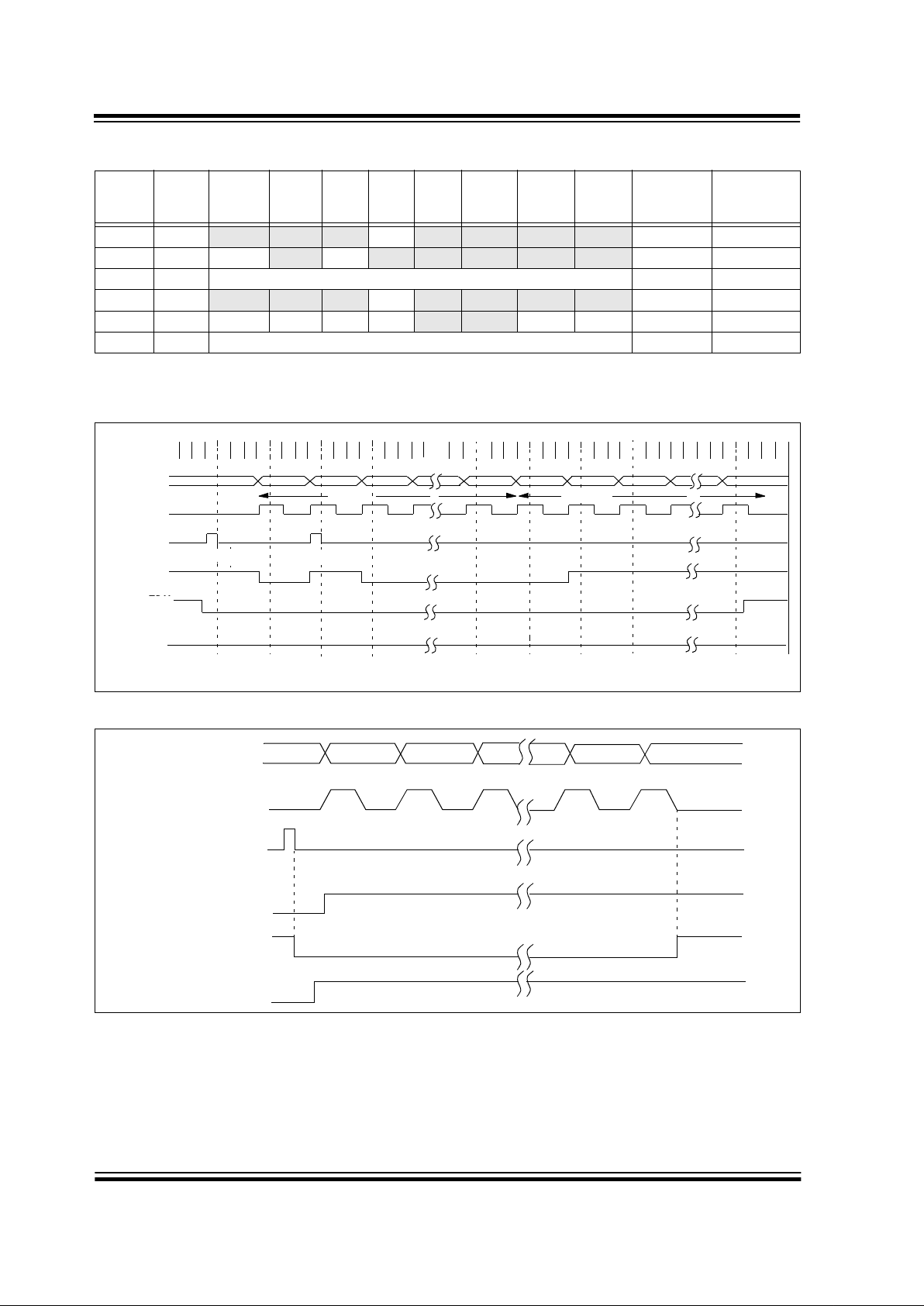
PIC16C745/765
DS41124A-page 84 Advanced Information
1999 Microchip Technology Inc.
TABLE 11-8: REGISTERS ASSOCIATED WITH SYNCHRONOUS MASTER TRANSMISSION
FIGURE 11-6: SYNCHRONOUS TRANSMISSION
FIGURE 11-7: SYNCHRONOUS TRANSMISSION (THROUGH TXEN)
Address Name Bit 7 Bit 6 Bit 5 Bit 4 Bit 3 Bit 2 Bit 1 Bi t 0
Val ue on:
POR,
BOR
Value on all
other Resets
0Ch PIR1
PSPIF
(1)
ADIF RCIF TXIF USBIF CCP1IF TMR2IF TMR1IF 0000 0000 0000 0000
18h RCSTA SPEN
RX9 SREN CREN — FERR OERR RX9D 0000 -00x 0000 -00x
19h TXREG USART Transmit Register 0000 0000 0000 0000
8Ch PIE1
PSPIE
(1)
ADIE RCIE TXIE USBIE CCP1IE TMR2IE TMR1IE 0000 0000 0000 0000
98h TXSTA CSRC TX9 TXEN SYNC
— BRGH TRMT TX9D 0000 -010 0000 -010
99h SPBRG Baud Rate Generator Register 0000 0000 0000 0000
Legend: x = unknown, - = unimplemented, read as '0'. Shaded cells are not used for synchronous master transmission.
Note 1: Bits PSPIE and PSPIF are reserved on the PIC16C745; always maintain these bits clear.
bit 0 bit 1 bit 7
WORD 1
Q1Q2Q3Q4Q1Q2Q3 Q4Q1 Q2Q3Q4Q1Q2Q3Q4Q1 Q2 Q3Q4 Q3Q4 Q1Q2 Q3Q4 Q1Q2 Q3Q4Q1Q2Q3Q4Q1 Q2Q3 Q4Q1Q2Q3Q4Q1 Q2Q3Q4
bit 2 bit 0 bit 1 bit 7
RC7/RX/DT pin
RC6/TX/CK pin
Write to
TXREG reg
TXIF bit
(Interrupt flag)
TRMT
TXEN bit
’1’ ’1’
Note: Sync master mode; SPBRG = ’0’. Continuous transmission of two 8-bit words
WORD 2
TRMT bit
Write word1
Write word2
RC7/RX/DT pin
RC6/TX/CK pin
Write to
TXREG reg
TXIF bit
TRMT bit
bit0
bit1
bit2
bit6 bit7
TXEN bit

1999 Microchip Technology Inc.
Advanced Information DS41124A-page 85
PIC16C745/765
11.3.2 USART SYNCHRONOUS MASTER
RECEPTION
Once synchronous mode is selected, reception is
enabled b y setting either enab le bit SREN (RCSTA<5>)
or enable bit CREN (RCSTA<4>). Data is sampled on
the RC7/RX/DT pin on the falling edge of the clock. If
enable bit SREN is set, then only a single word is
received. If enable bit CREN is set, the reception is
continuous until CREN is cleared. If both bits are set,
CREN takes preced ence. After cloc king the las t bit, the
received data in the Receive Shif t Register (RSR) is
transferred to the RCREG register (if it is empty). When
the transfer is complete, interrupt flag bit RCIF
(PIR1<5>) is set. The actual interrupt can be enabled/
disabled b y setting/clearing enab le bit RCIE (PIE1<5 >).
Flag bit RCIF is a read only bit, which is reset by the
hardware. In t his case, it is reset when t he RCREG register has been read and is empty. The RCREG is a double buffered register, i.e., it is a two deep FIFO. It is
possible for two bytes of data to be received and transferred to the RCREG FIFO and a third byte to begin
shifting into the R SR register . On th e clocking of the last
bit of the third byte, if the RCREG register is still full,
then overrun error bi t OERR (RCS TA<1> ) is set. The
word in the RSR will be lost. The RCREG register can
be read twice to retrieve the two bytes in the FIFO. Bit
OERR has to be cl eared in software (by clear ing bit
CREN). If bit OERR is set, transfers from the RSR to
the RCREG are inhibited, so it is essential to clear bit
OERR if it is set. The ninth receive bit is buffered the
same way as the receive data. Reading the RCREG
register will load bit RX9D wi th a new v alue , theref or e it
is essential for the user to read the RCSTA register
before reading RCREG in order not to lose the old
RX9D information.
Steps to follow when setting up a Synchronous Master
Reception:
1. Initialize the SPBRG register for the appropriate
baud rate. (Section 11.1)
2. Enable the synchronous master serial port by
setting bits SYNC, SPEN, and CSRC.
3. Ensure bits CREN and SREN are clear.
4. If interrupts are desired, then set enable bit RCIE.
5. If 9-bit reception is desired, then set bit RX9.
6. If a single reception is required, set bit SREN.
For continuous reception set bit CREN.
7. Interrupt fla g bit RCIF will be set when re ception
is complete and an interrupt will be generated if
enable bit RCIE was set.
8. Read the RCSTA register to get the ninth bit (if
enabled) and determine if any error occurred
during reception.
9. Read the 8-bit received data by reading the
RCREG register.
10. If any error occurred, clear the error by clearing
bit CREN.
TABLE 11-9: REGISTERS ASSOCIATED WITH SYNCHRONOUS MASTER RECEPTION
Address Name Bit 7 Bit 6 Bit 5 Bit 4 Bit 3 Bit 2 Bit 1 Bit 0
Value on:
POR,
BOR
Value on all
other Resets
0Ch PIR1
PSPIF
(1)
ADIF RCIF TXIF USBIF CCP1IF TMR2IF TMR1IF 0000 0000 0000 0000
18h RCSTA SPEN RX9
SREN CREN — FERR OERR RX9D 0000 -00x 0000 -00x
1Ah RCREG USART Receive Register 0000 0000 0000 0000
8Ch PIE1
PSPIE
(1)
ADIE RCIE TXIE USBIE CCP1IE TMR2IE TMR1IE 0000 0000 0000 0000
98h TXSTA CSRC
TX9 TXEN SYNC — BRGH TRMT TX9D 0000 -010 0000 -010
99h SPBR G Baud Rate Generator Register 0000 0000 0000 0000
Legend: x = unknown, - = unimplemented read as '0'. Shaded cells are not used for synchronous master reception.
Note 1: Bits PSPIE and PSPIF are reserved on the PIC16C745; always maintain these bits clear.

PIC16C745/765
DS41124A-page 86 Advanced Information
1999 Microchip Technology Inc.
FIGURE 11-8: SYNCHRONOUS RECEPTION (MASTER MODE, SREN)
CREN bit
RC7/RX/DT pin
RC6/TX/CK pin
Write to
bit SREN
SREN bit
RCIF bit
(interrupt)
Read
RXREG
Note: Timing diagram demonstrates SYNC master mode with bit SREN = ’1’ and bit BRG = ’0’.
Q3Q4Q1 Q2 Q3Q4 Q1 Q2Q3Q4Q2 Q1 Q2 Q3Q4Q1 Q2Q3 Q4 Q1Q2 Q3 Q4Q1 Q2 Q3Q4 Q1Q2 Q3 Q4Q1 Q2Q3Q4 Q1Q2 Q3 Q4
’0’
bit0 bit1 bit2 bit3 bit4 bit5 bit6 bit7
’0’
Q1Q2Q3 Q4

1999 Microchip Technology Inc.
Advanced Information DS41124A-page 87
PIC16C745/765
11.4 USART Synchronous Slave Mode
Synchronous sla v e mo de dif f ers fro m the M aster mod e
in the fact that the shift clock is supplied exter nally at
the RC6/TX/CK pin (inste ad of being suppl ied internally
in master mode). This allows the device to transfer or
receive data while in SLEEP mode. Slave mode is
entered by clearing bit CSRC (TXSTA<7>).
11.4.1 USART SYNCHRONOUS SLAVE
TRANSMIT
The operation of the synchronous master and slave
modes are identical, except in the case of the SLEEP
mode.
If two words are written to the TXREG and then the
SLEEP instruction is executed, the following will occur:
a) The first word will immediately transfer to the
TSR register and tran smit.
b) The second word will remain in TXREG register .
c) Flag bit TXIF will not be set.
d) When the first word has been shi fted out of TSR,
the TXREG register will transfer the second
word to the TSR and flag bit TXIF will now be
set.
e) If enable bit TXIE is set, the interrupt will wake
the chip from SLEEP and if the global interrupt
is enabled, the program will branch to the inter-
rupt vector (0004h).
Steps to follow when setting up a synchr onous slave
transmission:
1. En able the synchronou s sla v e serial port by set-
ting bits SYNC and SPEN and clearing bit
CSRC.
2. Clear bits CREN and SREN.
3. If interrupts are desired, then set enable bit
TXIE.
4. If 9-bit transmission is desired, set bit TX9.
5. Enable the transmission by setting enable bit
TXEN.
6. If 9-bit transmission is selected, the ninth bit
should be loaded in bit TX9D.
7. Start transmission by loading data to the
TXREG register.
11.4.2 USART SYNCHRONOUS SLAVE
RECEPTION
The operation of the synchronous master and slave
modes is identical, except in the case of the SLEEP
mode. Also, bit SREN is a don’t care in slave mode.
If receive is enabled by setting bit CREN prior to the
SLEEP instruction, a word may be received during
SLEEP. On completely receiving the word, the RSR
register will transfer the data to the RCREG register
and if enable bit RCIE bit is set, the interrupt generate d
will wake the chip from SLEEP. If the gl obal interrupt is
enabled, the p rog ram will branch to the interrupt vector
(0004h).
Steps to follow when setting up a Synchronous Slave
Reception:
1. Enable the synchronous master serial port by
setting bits SYNC and SPEN and clearing bit
CSRC.
2. If interrupts are desired, set enable bit RCIE.
3. If 9-bit reception is desired, set bit RX9.
4. To enable reception, set enable bit CREN.
5. Flag bit RCIF will be set when reception is com-
plete and an interrupt will be generated, if
enable bit RCIE was set.
6. Read the RCSTA register to get the ninth bit (if
enabled) and determine if any error occurred
during reception.
7. Read the 8-bit received data by reading the
RCREG register.
8. If any error occurred, clear the error by clearing
bit CREN.

PIC16C745/765
DS41124A-page 88 Advanced Information
1999 Microchip Technology Inc.
TABLE 11-10: REGISTERS ASSOCIATED WITH SYNCHRONOUS SLAVE TRANSMISSION
TABLE 11-11: REGISTERS ASSOCIATED WITH SYNCHRONOUS SLAVE RECEPTION
Address Name Bit 7 Bit 6 Bit 5 Bit 4 Bit 3 Bit 2 Bit 1 Bit 0
Val ue on:
POR,
BOR
Value on all
other Resets
0Ch PIR1
PSPIF
(1)
ADIF RCIF TXIF USBIF CCP1IF TMR2IF TMR1IF 0000 0000 0000 0000
18h RCSTA SPEN
RX9 SREN CREN — FERR OERR RX9D 0000 -00x 0000 -00x
19h TXREG USART Transmit Register 0000 0000 0000 0000
8Ch PIE1
PSPIE
(1)
ADIE RCIE TXIE USB IE CCP1IE TMR2IE TMR1IE 0000 0000 0000 0000
98h TXSTA CSRC TX9 TXEN SYNC
— BRGH TRM T TX9D 0000 -010 0000 -010
99h SPBRG Baud Rate Generator Register 0000 0000 0000 0000
Legend: x = unknown, - = unimplemented read as '0'. Shaded cells are not used for synchronous slave transmission.
Note 1: Bits PSPIE and PSPIF are reserved on the PIC16C745; always maintain these bits clear.
Address Name Bit 7 Bit 6 Bit 5 Bit 4 Bit 3 Bit 2 Bit 1 Bit 0
Val ue on:
POR,
BOR
Value on all
other Resets
0Ch PIR1
PSPIF
(1)
ADIF RCIF TXIF USBIF CCP1IF TMR2IF TMR1IF 0000 0000 0000 0000
18h RCSTA SPEN RX9
SREN CREN — FERR OERR RX9D 0000 -00x 0000 -00x
1Ah RCREG USART Receive Register 0000 0000 0000 0000
8Ch PIE1
PSPIE
(1)
ADIE RCIE TXIE USBIE CCP1IE TMR2IE TMR1IE 0000 0000 0000 0000
98h TXSTA CSRC
TX9 TXEN SYNC — BRGH TRMT TX9D 0000 -010 0000 -010
99h SPBRG Baud Rate Generator Register 0000 0000 0000 0000
Legend: x = unknown, - = unimplemented read as '0'. Shaded cells are not used for synchronous slave reception.
Note 1: Bits PSPIE and PSPIF are reserved on the PIC16C745; always maintain these bits clear.

1999 Microchip Technology Inc.
Advanced Information DS41124A-page 89
PIC16C745/765
12.0 ANALOG-TO-DIGITAL
CONVERTER (A/D) MODULE
The 8-bit Analog-To-Digital (A/D) con verter module ha s
five inputs for the PIC16C745 and eight for the
PIC16C765.
The A/D allows conversion of an analog input signal to
a corresponding 8-bit digital value. The output of the
sample and hold is the input into the conver ter, which
generates the result via succes sive a pproxi mation. The
analog reference voltage is software selectable to
either the device’s positive supply voltage (V
DD) or the
voltage level on the RA3/AN3/V
REF pin.
The A/D conv erter has a unique f eature of being ab le to
operate while the de vice is in SLEEP mode. To operate
in sleep, the A/D conversion clock must be derived from
the A/D’s dedicated internal RC oscillator.
The A/D module has three registers. These registers
are:
• A/D Result Register (ADRES)
• A/D Control Register 0 (ADCON0)
• A/D Control Register 1 (ADCON1)
The ADCON0 register, shown in Register 12-1, controls the operation of the A/D module. The ADCON1
register, shown in Register 12-2, configures the functions of the port pins. The port pins can be configured
as analog inputs (RA3 can al so be a v oltage re f erence)
or as digital I/O.
Additional inf o rmation on us ing the A/D mo dul e c an b e
found in the PICmicro™ Mid-Range MCU Family Reference Manual (DS33023) and in Application Note,
AN546.
REGISTER 12-1: A/D CONTROL REGISTER (ADCON0: 1Fh)
R/W-0 R/W-0 R/W-0 R/W-0 R/W-0 R/W-0 U-0 R/W-0
ADCS1 ADCS0 CHS2 CHS1 CHS0 GO/DONE — ADON R =Readable bit
W =Writable bit
U =Unimplemented bit,
read as ‘0’
- n = Value at POR reset
bit7 bit0
bit 7-6: ADCS<1:0>: A/D Conversion Clock Select bits
00 = F
INT/2
01 = F
INT/8
10 = F
INT/32
11 = F
RC (clock derived from dedicated internal oscillator)
bit 5-3: CHS<2:0>: Analog Channel Select bits
000 = channel 0, (RA0/AN0)
001 = channel 1, (RA1/AN1)
010 = channel 2, (RA2/AN2)
011 = channel 3, (RA3/AN3)
100 = channel 4, (RA5/AN4)
101 = channel 5, (RE0/AN5)
(1)
110 = channel 6, (RE1/AN6)
(1)
111 = channel 7, (RE2/AN7)
(1)
bit 2: GO/DONE: A/D Conversion Status bit
If ADON = 1
1 = A/D conversion in progress (setting this bit starts the A/D conversion)
0 = A/D conversion not in progress (This bit is automatically cleared by hardware when the A/D conver-
sion is comp lete)
bit 1: Unimplemented: Read as '0'
bit 0: ADON: A/D On bit
1 = A/D converter module is operating
0 = A/D converter module is shutoff and consumes no operating current
Note 1: A/D channels 5, 6 and 7 are implemented on the PIC16C765 only.

PIC16C745/765
DS41124A-page 90 Advanced Information
1999 Microchip Technology Inc.
REGISTER 12-2: A/D CONTROL REGISTER 1 (ADCON1: 9Fh)
U-0 U-0 U-0 U-0 U-0 R/W-0 R/W-0 R/W-0
— — — — — PCFG2 PCFG1 PCFG0 R = Readable bit
W =Writable bit
U = Unimplemented bit ,
read as ‘0’
- n = Value at POR
reset
bit7 bit0
bit 7-3: Unimplemented: Read as '0'
bit 2-0: PCFG<2:0>: A/D Port Configuration Control bits
A = Analog input
D = Digital I/O
PCFG<2:0> AN7 AN6 AN5 AN4 AN3 AN2 AN1 AN0 VREF
000 A AAAAAAAVDD
001 AAAAVREF AAARA3
010 D DDAAAAAVDD
011 DDDAVREF AAAAN3
100 D DDDADAAVDD
101 AAAAVREF AAAAN3
11x D DDDDDDDV
DD

1999 Microchip Technology Inc.
Advanced Information DS41124A-page 91
PIC16C745/765
The following steps should be followed for doing an A/D
conversion:
1. Configure the A/D module:
• Configure analog pins / voltage reference /
and digital I/O (ADCON1)
• Select A/D input channel (ADCON0)
• Select A/D conversion clock (ADCON0)
• Turn on A/D module (ADCON0)
2. Configure A/D interrupt ( i f desired):
• Clear ADIF bit
• Set ADIE bit
• Set GIE bit
3. Wait the required acquisition time.
4. Start conversion:
• Set GO/DONE
bit (ADCON0)
5. Wait for A/D conversion to complete, by either:
• Polling for the GO/DONE bit to be cleared
OR
• Waiting for the A/D interrupt
6. Read A/D result register (ADRES), clear bit
ADIF if required.
7. For next conversion, go to step 1 or step 2 as
required. The A/D conversion time per bit is
defined as T
AD. A minimum wait of 2TAD is
required before next acquisition starts.
FIGURE 12-1: A/D BLOCK DIAGRAM
(Input voltage)
V
IN
VREF
(Reference
voltage)
V
DD
PCFG<2:0>
CHS<2:0>
000 or
010 or
100 or
001 or
011 or
101
RE2/AN7(1)
RE1/AN6(1)
RE0/AN5(1)
RA5/AN4
RA3/AN3/V
REF
RA2/AN2
RA1/AN1
RA0/AN0
111
110
101
100
011
010
001
000
A/D
Conver ter
Note 1: Not available on PIC16C745.
11x

PIC16C745/765
DS41124A-page 92 Advanced Information
1999 Microchip Technology Inc.
12.1 A/D Acquisition Requirements
For the A/D converter to meet its specified accuracy,
the charge holding capacitor (CHOLD) must be allowed
to fully charge to the input channel voltage level. The
analog input model is shown in Figure 12-2. The
source impedance (R
S) and the internal sampling
switch (RSS) impedance directly affect the time
required to charge the capacitor C
HOLD. The sampling
switch (RSS) impedance varies over the de vic e voltage
(V
DD), Figure 12-2. The source impedance affects the
offset voltage at the analog input (due to pin leak age
current).
The maximum recommended impedance for analog sources is 10 kΩ. After the analog input channel is
selected (changed), the acquisition must pass before
the conversion can be started.
To calculate the minimum acquisition time,
Equation 12-1 may be used. This equation assumes
that 1/2 LSb error is used (512 steps for the A/D). The
1/2 LSb error is the max im um erro r all o wed for the A/D
to meet its specified resolution.
To calculate the minimum acquisition time, T
ACQ, see
the PICmicro™ Mid-Range MCU Family Reference
Manual (DS33023). In general, however, given a max
of 10kΩ and a worst case temperature of 100°C, T
ACQ
will be no more than 16µsec.
FIGURE 12-2: ANALOG INPUT MODEL
EQUATION 12-1: ACQUISITION TIME
CPIN
VA
Rs
ANx
5 pF
V
DD
VT = 0.6V
V
T = 0.6V
I leakage
R
IC ≤
1k
Sampling
Switch
SS
R
SS
CHOLD
= DAC capacitance
V
SS
6V
Sampling Switch
5V
4V
3V
2V
5 6 7 8 9 10 11
(kΩ)
VDD
= 51.2 pF
± 500 nA
Legend CPIN
VT
I leakage
R
IC
SS
C
HOLD
= input capacitance
= threshold voltage
= leakage current at the pin due to
= interconnect resistance
= sampling switch
= sample/hold capacitance (from DAC)
various junctions
TACQ ==Amplifier Settling Time +
Hold Capacitor Charging Tim e +
Temperature Coefficient
TAMP + TC + TCOFF
TAMP = 5µS
T
C = - (51.2pF)(1kΩ + RSS + RS) In(1/511)
T
COFF = (Temp -25°C)(0.05µS/°C)

1999 Microchip Technology Inc.
Advanced Information DS41124A-page 93
PIC16C745/765
12.2 Selecting the A/D Conversion Clock
The A/D conversion time per bit is defined as TAD. The
A/D conversion re quires 9.5T
AD per 8-bit conversion .
The source of the A/D conversion clock is software
selectable. The four possible options for TAD are:
•2T
OSC
•8TOSC
•32TOSC
• Dedicated Internal RC oscillator
For correct A/D conversions, the A /D co nversion clock
(T
AD) must be select ed to ens ure a min imum TAD time
of 1.6 µs.
TABLE 12-1: TAD vs. DEVICE OPERATING FREQUENCIES
12.3 C
onfiguring Analog Port Pins
The ADCON1, TRISA and TRISE registers control the
operation of the A/D por t pins. The port pins that are
desired as analog inputs must have their correspon ding
TRIS bits set (input). If the TRIS bit is cleared (output),
the digital output level (VOH or VOL) will be converted.
The A/D operation is independent of the state of the
CHS<2:0> bits and the TRIS bits.
12.4 A/D Conversions
Clearing the GO/DONE bit during a conversion will
abort the current conversion. The ADRES register will
NOT be updated with the partially completed A/D conversion sample. That is, the ADRES register will continue to contain the value of the last completed
conversi on (or the l ast v alue w ritten to the ADRES register). After the A/D conversion is aborted, a 2T
AD wait
is required before the next acquisition is star ted. After
this 2T
AD wait, an acqu isition is aut omatically s tarted on
the selected channel.
AD Clock Source (T
AD) Device Frequency
Operation ADCS1:ADCS0 20 MHz 5 MHz 1.25 MHz 333.33 kHz
2TOSC 00 100 ns
(2)
400 ns
(2)
1.6 µs6 µs
8TOSC 01 400 ns
(2)
1.6 µs6.4 µs 24 µs
(3)
32TOSC 10 1.6 µs6.4 µs 25.6 µs
(3)
96 µs
(3)
RC 11 2 - 6 µs
(1,4)
2 - 6 µs
(1,4)
2 - 6 µs
(1,4)
2 - 6 µs
(1)
Note1: The RC source has a typical TAD time of 4 µs.
2: Th ese values violat e the minimum required T
AD time.
3: For faster conversion times, the selection of another clock source is recommended.
4: For device frequencies above 1 MHz, the device must be in SLEEP for the entire conversion, or the A/D
accuracy may be out of specification.
Note 1: When reading the port register, all pins
configured as analog input channels will
read as cleared (a low level). Pins configured as dig ital in puts w ill c onver t an ana log input. Analog levels on a digitally
configured input will not affect the conversion accuracy.
2: Analog levels on any pin that is defined as
a digital input, but not as an analog input,
may cause the input buffer to consume
current that is out of specification.
3: The TRISE register is not provided on the
PIC16C745.
Note: The GO/DONE bit should NOT be set in
the same instruction that turns on the A/D.

PIC16C745/765
DS41124A-page 94 Advanced Information
1999 Microchip Technology Inc.
12.5 A/D Operation During Sleep
The A/D module can operate during SLEEP mode.
This requires that the A/D clock source be set to RC
(ADCS<1:0> = 11). When the RC clock source is
selected, the A/ D module waits one i nstruction c ycle
before starting the conversion. This allows the SLEEP
instruction to be executed, whi ch eli min at es all di gi tal
switching noise from the conversion. When the conversion is completed, the GO/DONE
bit will be
cleared, and the result loaded into the ADRES register. If the A/D interrupt is enabled, the device will
wake-up from SLEEP. If the A/D interrupt is not
enabled, the A/D module will then be turned off,
although the ADON bit will r ema in se t.
When the A/D cloc k sou rce is ano ther clo c k opti on (not
RC), a SLEEP instruction will cause the present con v ersion to be aborted and the A/D modul e to be turned off ,
though the ADON bit will remain set.
Turning off the A/D places the A/D module in its lowest
current consumption state.
12.6 Effects of a RESET
A device reset forces all registers to their reset state.
The A/D module is disabled and any conversion in
progress is aborted. All pins with analog functions are
configured as available inputs.
The ADRES reg ist er wi ll co nta in unk nown d ata af te r a
power-on reset.
12.7 Use of the CCP Trigg e r
An A/D conversion can be started by the “special event
trigger” of the CCP2 module. This requires that the
CCP2M<3:0> bits (CCP2CON<3:0>) be programmed as
1011 and that the A/D module is enabled (ADON bit is
set). When the trigger occurs, the GO/D ONE
bit will be
set, starting the A/D conversion, and the Timer1 counter
will be reset to zero. Timer1 is reset to automatically
repeat the A/D acquisition period with minimal soft ware
overhead (moving the ADRES to the desired location).
The appropriate analog input channel must be selected
and the minimum acquisition done before the “special
event trigger” sets the GO/DONE
bit (starts a conversion).
If the A/D module i s not enabled (ADON is cle ared),
then the “spe cial event tr igger” w ill be ignore d by the
A/D module, but will still reset th e Tim er 1 cou nt er.
TABLE 12-2: SUMMARY OF A/D REGISTERS
Note: For the A/D module to operate in SLEEP,
the A/D clock source must be set to RC
(ADCS<1:0> = 11). To perform an A/D
conversion in SLEEP, ensure the SLEEP
instruction immediately follows the instruction that sets the GO/DONE
bit.
Address Name Bit 7 Bit 6 Bit 5 Bit 4 Bit 3 Bit 2 Bit 1 Bit 0
Value on:
POR,
BOR
Value on all
other
Resets
0Bh,8Bh,
10Bh,18Bh
INTCON GIE PEIE
T0IE INTE RBIE T0IF INTF RBIF 0000 000x 0000 000u
0Ch
PIR1
PSPIF
(1)
ADIF RCIF TXIF USBIF CC P1IF TMR2IF TMR1IF 0000 0000 0000 0000
8Ch
PIE1
PSPIE
(1)
ADIE RCIE TXIE USBIE CCP1IE TMR2IE TMR1IE 0000 0000 0000 0000
1Eh
ADRES A/D Result Register xxxx xxxx uuuu uuuu
1Fh
ADCON0 ADCS1 ADCS0 CHS2 CHS1 CHS0 GO/
DONE
—ADON0000 00-0 0000 00-0
9Fh
ADCON1
— — — — — PCFG2 PCFG1 PCFG0 ---- -000 ---- -000
05h PORTA
— — RA5 RA4 RA3 RA2 RA1 RA0
--0x 0000 --0u 0000
85h TRISA
— — PORTA Data Direction Register
--11 1111 --11 1111
09h PORTE
— — — — —
RE2
(1)
RE1
(1)
RE0
(1)
---- -xxx ---- -uuu
89h TRISE
IBF
(1)
OBF
(1)
IBOV
(1)
PSP-MODE
(1)
—
PORTE
(1)
Data Direction Bits
0000 -111 0000 -111
Legend: x = unknown, u = unchanged, - = unimplemented read as '0'. Shaded cells are not used for A/D conversion.
Note 1: These bits are reserved on the PIC6C745; always maintain these bits clear.

1999 Microchip Technology Inc.
Advanced Information DS41124A-page 95
PIC16C745/765
13.0 SPECIAL FEATURES OF THE
CPU
What sets a microcontroller apar t from other processors are special circuits to deal with the needs of realtime applications. The PIC16C745/765 family has a
host of such f eature s intende d to maxi mize system reliability, minimize cost through elimination of external
components, provide power saving operating modes
and offer code protection. These are:
• Oscillator selection
• Reset
- Power-on Reset (POR)
- Powe r-up Timer (PWRT)
- Oscillator Start-up Timer (OST)
- Brown-out Reset (BOR)
• Interrupts
• Watchdog Timer (WDT)
• SLEEP
• Code protection
• ID locations
• In-Circuit Serial Programming™ (ICSP)
The PIC16C745/765 has a Watchdog Timer, which can
be shut off only through configuration bits. It runs off its
own dedicated RC oscillator for added reliabili ty. There
are two timers that offer necessary delays on power-up.
One is the Oscillator Start-up Timer (OST), intended to
keep the chip in reset until the crystal oscillator is stable.
The other is the Power-up Timer (PWRT), which provides a fixed delay of 72 ms (nominal) on power-up only
and is designed to keep the part in reset, while the
power supply stabilizes. With these t wo timer s on -ch ip,
most applications need no external reset circuitry.
SLEEP mode is designed to offer a very low current
power-down m ode. The user can wake-up from SLEEP
through external reset, WDT wake-up or through an
interrupt. Several oscillator options are also made
available to allow the part to fit the application. The EC
oscillator allow s the user to directl y driv e the mi croco ntroller, while the HS oscillator allows the use of a high
speed crystal/resonator. A set of configuration bits a re
used to select various options.
13.1 Configuration Bits
The configurati on bits can be prog ra mmed (read as '0')
or left unprogrammed (read as '1') to select various
device configurations. These bits are mapped in program memory location 2007h.
The user will note that address 2007h is beyond the user
program memory space. In fact, it belongs to the special
test/configuration memory space (2000h - 3FFFh),
which can be accessed only during programming.
REGISTER 13-1: CONFIGURATION WORD
CP1 CP0 CP1 CP0 CP1 CP0 — —CP1CP0PWRTEWDTE FOSC1 FOSC0
Register: CONFIG
Address 2007h
bit13 bit0
bit 13-12: CP<1:0>: Code Protection bits
(1)
11-10:00 = All memory is code protected
9-8: 01 = Upper 3/4th of program memory code protected
5-4: 10 = Uppe r half of program memory code protected
11 = Code protection off
bit 7-6: Unimplemented: Read as ’1’
bit 3: PWRTE
: Power-up Timer Enable bit
1 = PWRT disabled • No delay after Power-up reset or Brown-out reset
0 = PWRT enabled • A delay of 4x WDT (72 ms) is present after Power-up and Brown-out
bit 2: WDTE: Watchdog Timer Enable bit
1 = WDT enabled
0 = WDT disabled
bit 1-0: FOSC<1:0>: Oscillator Selection
00 - HS- HS osc
01 - EC- External clock. CLKOUT on OSC2 pin
10 - H4- HS osc with 4x PLL enabled
11 - E4- External clock with 4x PLL enabled. CLKOUT on OSC2 pin
Note1: All of the CP<1:0> pairs have to be given the same value to enable the code protection scheme listed.

PIC16C745/765
DS41124A-page 96 Advanced Information
1999 Microchip Technology Inc.
13.2 Oscillator Configurations
13.2.1 OSCILLATOR TYPES
The PIC16C745/765 can be operated in four different
oscillator modes . The user c an progra m a configu ration
bit (FOSC0) to select one of these four modes:
•EC External Clock
•E4 External Clock with PLL
•HS High Speed Crystal/Resonator
•H4 High Speed Crystal/Resonator with PLL
13.2.2 CRYSTAL OSCILLATOR/CERAMIC
RESONATORS
In HS mode, a crystal or ceramic resonator is connected to the OSC1/CLKIN and OSC2/CLKOUT pins to
establish oscillation (Figure 13-1). The PIC16C745/
765 oscillator design requires the use of a parallel cut
crystal. Use of a series cut crystal may giv e a frequenc y
out of the crystal manuf acturers s pecifications . When in
HS mode, the de vice can ha ve an e xternal clock so urce
to drive the OSC1/CLKIN pin (Figure 13-2). In this
mode, the oscillator start-up timer is active for a period
of 1024*T
OSC. See the PICmicro™ Mid-Range MCU
Reference Man ual (DS3 3023) f or deta ils on b uilding a n
external oscillator.
FIGURE 13-1: CRYSTAL/CERAMIC
RESONATOR OPERATION
(HS OSC CONFIGURATION)
TABLE 13-1: CERAMIC RESONATORS
TABLE 13-2: CAPACITOR SELECTION FOR
CRYSTAL OSCILLATOR
13.2.3 H4 MODE
In H4 mode, a PLL module is switched on in-line with
the clock prov ided across OSC1 and OCS2. The output
of the PLL drives F
INT.
C1
C2
XTAL
OSC2
Note1
OSC1
Rf
SLEEP
To inter nal
logic
PIC16C745/765
Rs
Note 1: A series resistor may be required for AT strip cut
crystals.
Ranges Tested:
Mode Freq OSC1 OSC2
HS 6.0 MHz TBD TBD
These values are for design guidance only. See notes at
bottom of page.
Osc Type Crystal
Freq
Cap. Range C1Cap. Range
C2
HS 6.0 MHz
TBD TBD
These values are for design guidance only. See notes at
bottom of page.
Note 1: Higher capacitance increases the stability
of the oscillator, but also increases the startup time.
2: Since each resonator/crys tal has its own
characteristics, the user should consult the
resonator/crystal manufacturer for appro priate values of external components.
3: Rs may be required in HS mode to avoid
overdriving crystals with low drive level
specification.
4: When migrating from other PICmicro
devices, oscillator performance should be
verified.
5: Users should consult the USB Specificatio n
1.0 to ensure their resonator/crystal oscillator meets the required jitter limits for USB
operation.

1999 Microchip Technology Inc.
Advanced Information DS41124A-page 97
PIC16C745/765
13.2.4 EXTERNAL CLOCK IN
In EC mode, users may directly drive the PIC16C745/
765 provided that this external clock source meets the
AC/DC timing requirements listed in Section 17.4.
Figure 13-2 below shows how an external clock circuit
should be configured.
FIGURE 13-2: EXTERNAL CLOCK INPUT
OPERATION (EC OSC
CONFIGURATION)
13.2.5 E4 MODE
In E4 mode, a PLL m odule is switch ed on in-l ine with
the clock provided to OSC1. The output of the PLL
drives FINT.
FIGURE 13-3: OSCILLATOR/PLL CLOCK CONTROL
13.3 Reset
The PIC16CXX differentiates between various kinds of
reset:
• Power-on Reset (POR)
•MCLR
reset during normal operation
•MCLR reset during SLEEP
• WDT Reset (normal operation)
• Brown-out Reset (BOR)
Some registers are not affected in any reset condition;
their status is unkno w n on POR and unc han ged in any
other reset. Most other registers are reset to a “reset
state” on POR, on the MCLR
and WDT Reset, on
MCLR
reset during SLEEP, and on BOR. The TO and
PD
bits are set or cleared differently in different reset
situations as indicated in Table 13-4. These bits are
used in software to determine the nature of the reset.
See Table 13-7 for a full d escription of reset states of al l
registers.
A simplified bloc k diag ram of the on-ch ip res et circui t is
shown in Figure 13-4.
The PICmicro
®
devices h ave a MCLR noise filter in the
MCLR
reset path. The fil ter will detec t and ignore smal l
pulses.
It should be noted that a WDT reset does not drive
MCLR
pin low.
Clock from
ext. system
PIC16C745/765
OSC1
OSC2/CLKOUT
CLKOUT
Note: CLKOUT is the same frequency as OSC1 if
in E4 mode, otherwise CLKOUT = OSC1/4.
OSC2
OSC1
EC
E4
HS
H4
4x PLL
6 MHz
Q Clock
Generator
To Circuits
24 MHz
F
INT
EC
E4
HS
H4

PIC16C745/765
DS41124A-page 98 Advanced Information
1999 Microchip Technology Inc.
FIGURE 13-4: SIMPLIFIED BLOCK DIAGRAM OF ON-CHIP RESET CIRCUIT
S
R
Q
External
Reset
MCLR
VDD
OSC1
WDT
Module
V
DD rise
detect
OST/PWRT
Dedicated
RC OSC
Time-out
Power-on Reset
OST
10-bit Ripple counter
PWRT
Chip Reset
10-bit Ripple counter
Reset
Enable OST
Enable PWRT
SLEEP
Brown-out
Reset
On-chip

1999 Microchip Technology Inc.
Advanced Information DS41124A-page 99
PIC16C745/765
13.4 Resets
13.4.1 POWER-ON RESET (POR)
A Power-on Reset pulse is generated on-chip when
V
DD rise is detected (in the range of 1.5V - 2.1V). To
take advantage of the POR, just tie the MCLR
pin
directly (or through a resistor) to V
DD. This will elimi-
nate external RC components usu ally needed to create
a POR. A maximum rise time for V
DD is specified. See
Electrical Specifications for details.
When the device starts normal operation (exits the
reset condition), device operating parameters (v ol tage,
frequency, temperature) must be met to ensure operation. If these cond itions are not m et, the d ev ice mus t be
held in reset until the operating conditions are met.
Brown-out re set may be used to meet th e s t artup con ditions.
For additional information, refer to Application Note
AN607, “
Power-up Trouble Shooting
.”
13.4.2 POWER-UP TIMER (PWRT)
The Power-up Timer provides a fixed 72 ms nominal
time-out on power-up from the POR. The PWRT operates on an internal RC oscillator. The device is kept in
reset as long as the PWRT is active. The PWRT’s time
delay allows V
DD to rise to an acceptable level. A con-
figuration bit is provided to enable/disable the PWRT.
The power-up time de la y will v ary from chip to chip due
to V
DD, temperature and process variation. See DC
parameters for details (T
PWRT, parameter #33).
13.4.3 OSCILLATOR START-UP TIMER (OST)
The Oscillator Start-up Timer provides a delay of 1024
oscillator cycles (from OSC1 input) after the PWRT
delay. This ensures that the crystal oscilla tor or resonator has started and stabilized.
The OST time-out is in voked on ly for HS mod e and only
on power-on reset or wake-up from SLEEP.
13.4.4 BROWN-OUT RESET (BOR)
If V
DD falls below VBOR (parameter D005) for longer
than T
BOR (parameter #35), the brown-out situation
will reset the device. If V
DD fall s b el ow VBOR fo r l es s
than T
BOR, a reset may not occur.
Once the brown-out occ urs, the device wil l remain i n
brown-out reset until VDD rises above VBOR. The
power-up timer then keeps the device in reset for
T
PWRT (parameter #33). If VDD should fall below VBOR
during TPWRT, the brown-out reset process will restart
when V
DD rises above VBOR with the power-up timer
reset. Since the device is intended to operat e at 5V
nominal only, the brown-out detect is always enabled
and the device will reset when Vdd falls below the
brown-out threshol d. This device is uniqu e in th at the
4•WDT timer will not activate after a brown-out if
PWRTE
= 1 (inactive).
13.4.5 TIME-OUT SEQUENCE
On power-up, the time-out sequence is as follow s: The
PWRT delay starts (if enabled) when a POR reset
occurs. Then OST starts counting 1024 oscillator
cycles when PWRT ends (HS). When the OST ends,
the device comes out of RESET.
If MCLR
is kept low long enough, the time-outs will
expire. Bringing MCLR
high will begin execution immediately . This is useful f or testing pu rposes or to synchronize more than one PIC16CXX device operating in
parallel.
Table 13-5 shows the reset conditions for the STATUS,
PCON and PC registers, while Table 13-7 shows the
reset conditions for all the registers.
13.4.6 POW ER CONTROL/STATUS REGISTER
(PCON)
The Brown-out Reset Status bit, BOR
, is unknown on a
POR. It must be set b y the u ser and c hec ked on subs equent resets to see if bit BO R was c leare d, indi cating a
BOR occurred. The BOR
bit is not predictable if the
brown-out reset circuitry is disabled.
The Power-on Reset Status bit, POR, is cleared on a
POR and unaffected otherwise. The user must set this
bit following a POR and check it on subsequent resets
to see if it has been cleared.

PIC16C745/765
DS41124A-page 100 Advanced Information
1999 Microchip Technology Inc.
13.5 Time-out in Various Situations
TABLE 13-3: RESET TIME-OUTS
TABLE 13-4: STATUS BITS AND THEIR SIGNIFICANCE
TABLE 13-5: RESET CONDITION FOR SPECIAL REGISTERS
Oscillator
Configuration
POR BORt
Wake-up
from SLEEP
PWRTE
= 0 PWRTE = 1 PWRTE = 0 PWRTE = 1
HS TPWRT + 1024•TOSC 1024•TOSC TPWRT + 1024•TOSC 1024•TOSC 1024•TOSC
H4 TPWRT + TPLLRT +
1024•T
OSC
TPLLRT + 1024•TOSC TPWRT + TPLLRT +
1024•T
OSC
TPLLRT + 1024•TOSC TPLLRT +
1024•T
OSC
EC TPWRT 0TPWRT 00
E4 T
PWRT + TPLLRT TPLLRT TPWRT + TPLLRT TPLLRT TPLLRT
POR BOR TO PD
0x11Power-on Reset
0x0xIllegal, TO
is set on POR
0xx0Illegal, PD is set on POR
1011Brown-out R eset
1101WDT Reset
1100WDT Wake-up
11uuMCLR
Reset during normal operation
1110MCLR
Reset during SLEEP or interrupt wake-up from SLEEP
Condition
Program
Counter
STATUS
Register
PCON
Register
Power-on Reset 000h 0001 1xxx ---- --0x
MCLR Reset during normal operation 000h 000u uuuu ---- --uu
MCLR
Reset during SLEEP 000h 0001 0uuu ---- --uu
WDT Reset 000h 0000 1uuu ---- --uu
WDT Wake-up PC + 1 uuu0 0uuu ---- --uu
Brown-out Reset 000h 000x xuuu ---- --u0
Interrupt wake-up from SLEEP PC + 1
(1)
uuu1 0uuu ---- --uu
Legend: u = unchanged, x = unknown, - = unimplemented bit read as ’0’.
Note 1: When the wake-up is due to an interrupt and the GIE bit is set, the PC is loaded with the interrupt vector
(0004h).
TABLE 13-6: REGISTERS ASSOCIATED WITH RESETS
Address NameBit 7Bit 6Bit 5Bit 4Bit 3Bit 2Bit 1Bit 0
Valu e on:
POR, BOR
Value on all
other resets
03h, 83h,
103h, 183h
Status IRP RP1 RP0 TO
PD ZDCC0001 1xxx 000q quuu
8Eh PCON
— — — — — —
POR
BOR
---- --qq ---- --uu
Legend: x = unknown, u = unchanged, - = unimplemented locations read as '0'.
 Loading...