

Page 1
MCP3421
1 8 - Bi t A na l o g -t o - D ig i t a l C o n v er t e r
with I2C Interface and On-Board Reference
Features
• 18-bit ΔΣ ADC in a SOT-23-6 package
• Differential input operation
• Self calibration of Internal Offset and Gain per
each conversion
• On-board Voltage Reference:
- Accuracy: 2.048V ± 0.05%
- Drift: 5 ppm/°C
• On-board Programmable Gain Amplifier (PGA):
- Gains of 1,2,4 or 8
• On-board Oscillator
• INL: 10 ppm of FSR (FSR = 4.096V/PGA)
• Programmable Data Rate Options:
- 3.75 SPS (18 bits)
- 15 SPS (16 bits)
- 60 SPS (14 bits)
- 240 SPS (12 bits)
• One-Shot or Continuous Conversion Options
• Low current consumption:
- 145 µA typical
= 3V, Continuous Conversion)
(V
DD
- 39 µA typical
= 3V, One-Shot Conversion with 1 SPS)
(V
DD
• Supports I2C Serial Interface:
- Standard, Fast and High Speed Modes
• Single Supply Operation: 2.7V to 5.5V
• Extended Temperature Range: -40°C to 125°C
Typical Applications
Description
The MCP3421 is a single channel low-noise, high
accuracy ΔΣ A/D converter with differential inputs and
up to 18 bits of resolution in a small SOT-23-6 package.
The on-board precision 2.048V reference voltage
enables an input range of ±2.048V differentially
(Δ voltage = 4.096V). The device uses a two-wire I
compatible serial interface and operates from a single
2.7V to 5.5V power supply.
The MCP3421 device performs conversion at rates of
3.75, 15, 60, or 240 samples per second (SPS)
depending on the user controllable configuration bit
settings using the two-wire I
device has an on-board programmable gain amplifier
(PGA). The user can select the PGA gain of x1, x2, x4,
or x8 before the analog-to-digital conversion takes
place. This allows the MCP3421 device to convert a
smaller input signal with high resolution. The device
has two conversion modes: (a) Continuous mode and
(b) One-Shot mode. In One-Shot mode, the device
enters a low current standby mode automatically after
one conversion. This reduces current consumption
greatly during idle periods.
The MCP3421 device can be used for various high
accuracy analog-to-digital data conversion applications
where design simplicity, low power, and small footprint
are major considerations.
2
C serial interface. This
2
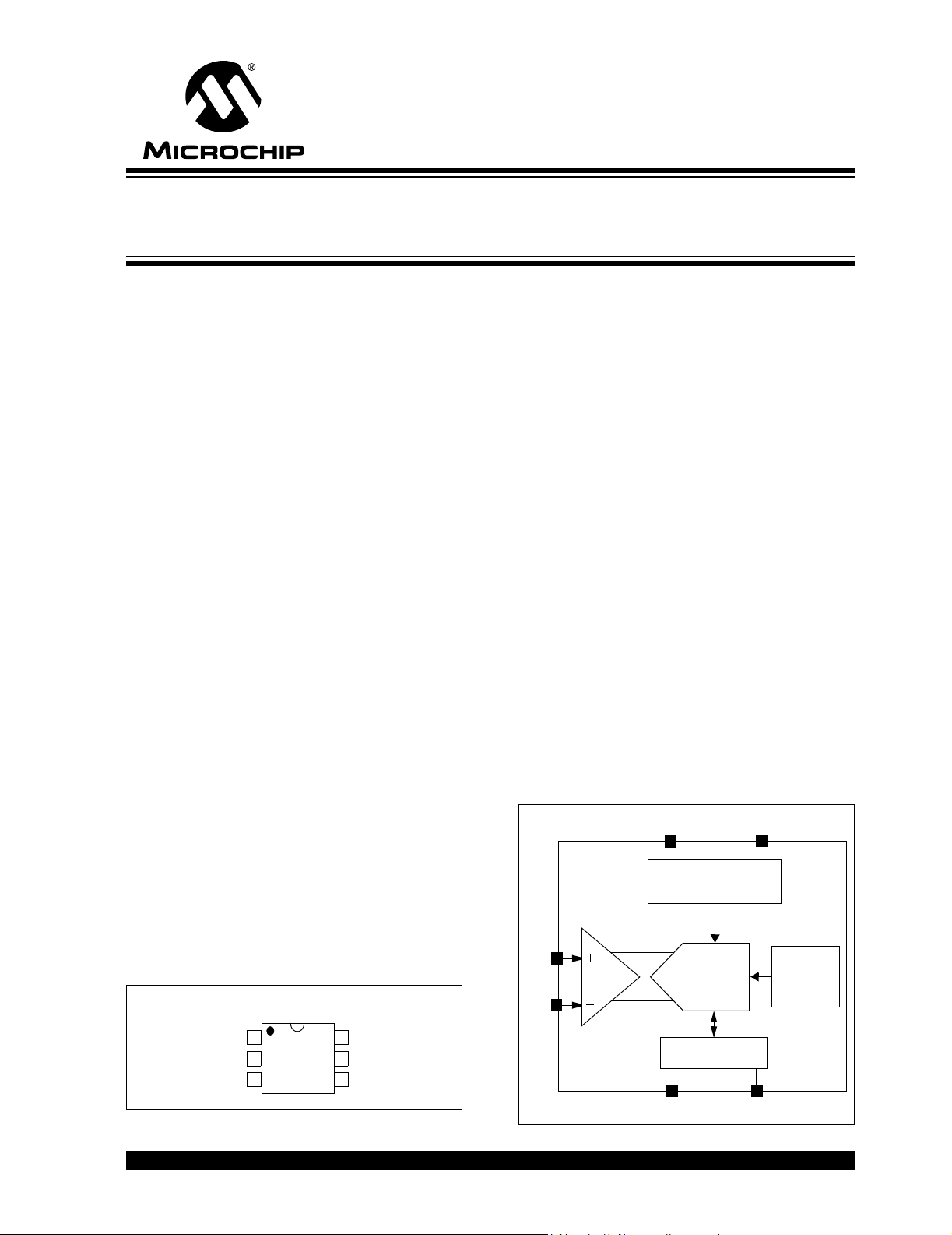
Block Diagram
V
SS
V
DD
C
• Portable Instrumentation
• Weigh Scales and Fuel Gauges
• Temperature Sensing with RTD, Thermistor, and
Thermocouple
• Bridge Sensing for Pressure, Strain, and Force.
Package Types
SS
Top View
1
2
3
6
5
4
V
IN
V
DD
SDA
-
SOT-23-6
VIN+
V
SCL
© 2006 Microchip Technology Inc. DS22003B-page 1
Gain = 1, 2, 4, or 8
VIN+
PGA
VIN-
Voltage Reference
(2.048V)
V
REF
ΔΣ ADC
Converter
2
C Interface
I
SCL
SDA
Clock
Oscillator
Page 2
MCP3421
1.0 ELECTRICAL CHARACTERISTICS
Absolute Maximum Ratings†
VDD...................................................................................7.0V
All inputs and outputs w.r.t V
Differential Input Voltage ...................................... |V
Output Short Circuit Current ................................. Continuous
Current at Input Pins ....................................................±2 mA
Current at Output and Supply Pins ............................±10 mA
Storage Temperature.....................................-65°C to +150°C
Ambient Temp. with power applied ...............-55°C to +125°C
ESD protection on all pins ................ ≥ 6kV HBM, ≥ 400V MM
Maximum Junction Temperature (T
............... –0.3V to VDD+0.3V
SS
) ..........................+150°C
J
DD
- VSS|
†Notice: Stresses above those listed under “Maximum Ratings” may cause permanent damage to the device. This is a
stress rating only and functional operation of the device at
those or any other conditions above those indicated in the
operational listings of this specification is not implied.
Exposure to maximum rating conditions for extended periods
may affect device reliability
.
ELECTRICAL CHARACTERISTICS
Electrical Specifications: Unless otherwise specified, all parameters apply for TA = -40°C to +85°C, VDD = +5.0V, VSS = 0V,
V
+ = VIN- = V
IN
Parameters Sym Min Typ Max Units Conditions
Analog Inputs
Differential Input Range — ±2.048/PGA — V V
Common-Mode Voltage Range
(absolute)
Differential Input Impedance
(Note 2)
Common Mode input
Impedance
System Performance
Resolution and No Missing
(Note 8)
Codes
Data Rate
Output Noise — 1.5 — µV
Note 1: Any input voltage below or greater than this voltage causes leakage current through the ESD diodes at the input pins.
2: This input impedance is due to 3.2 pF internal input sampling capacitor.
3: The total conversion speed includes auto-calibration of offset and gain.
4: INL is the difference between the endpoints line and the measured code at the center of the quantization band.
5: Includes all errors from on-board PGA and V
6: Full Scale Range (FSR) = 2 x 2.048/PGA = 4.096/PGA.
7: This parameter is ensured by characterization and not 100% tested.
8: This parameter is ensured by design and not 100% tested.
/2. All ppm units use 2*V
REF
(Note 1)
Z
IND
Z
INC
(Note 3)
This parameter is ensured by characterization and not 100% tested.
DR 176 240 328 SPS S1,S0 = ‘00’, (12 bits mode)
as full-scale range.
REF
VSS-0.3 — VDD+0.3 V
(f) — 2.25/PGA — MΩ During normal mode operation
(f) — 25 — MΩ PGA = 1, 2, 4, 8
12 — — Bits DR = 240 SPS
14 — — Bits DR = 60 SPS
16 — — Bits DR = 15 SPS
18 — — Bits DR = 3.75 SPS
44 60 82 SPS S1,S0 = ‘01’, (14 bits mode)
11 15 20.5 SPS S1,S0 = ‘10’, (16 bits mode)
2.75 3.75 5.1 SPS S1,S0 = ‘11’, (18 bits mode)
.
REF
RMSTA
PGA = 1, V
= VIN+ - VIN-
IN
= 25°C, DR = 3.75 SPS,
IN
= 0
DS22003B-page 2 © 2006 Microchip Technology Inc.
Page 3
MCP3421
ELECTRICAL CHARACTERISTICS (CONTINUED)
Electrical Specifications: Unless otherwise specified, all parameters apply for TA = -40°C to +85°C, VDD = +5.0V, VSS = 0V,
V
+ = VIN- = V
IN
Parameters Sym Min Typ Max Units Conditions
Integral Nonlinearity
Internal Reference Voltage V
Gain Error
PGA Gain Error Match
Gain Error Drift
Offset Error V
Offset Drift vs. Temperature — 50 — nV/°C V
Common-Mode Rejection — 105 — dB at DC and PGA =1,
Gain vs. V
DD
Power Supply Rejection at DC — 100 — dB T
Power Requirements
Voltage Range V
Supply Current during
Conversion
Supply Current during Standby
Mode
2
C Digital Inputs and Digital Outputs
I
High level input voltage V
Low level input voltage V
Low level output voltage V
Hysteresis of Schmitt Trigger
for inputs
(Note 7)
Supply Current when I
line is active
Input Leakage Current I
Pin Capacitance and I
Pin capacitance C
2
C Bus Capacitance C
I
Thermal Characteristics
Specified Temperature Range T
Operating Temperature Range T
Storage Temperature Range T
Note 1: Any input voltage below or greater than this voltage causes leakage current through the ESD diodes at the input pins.
2: This input impedance is due to 3.2 pF internal input sampling capacitor.
3: The total conversion speed includes auto-calibration of offset and gain.
4: INL is the difference between the endpoints line and the measured code at the center of the quantization band.
5: Includes all errors from on-board PGA and V
6: Full Scale Range (FSR) = 2 x 2.048/PGA = 4.096/PGA.
7: This parameter is ensured by characterization and not 100% tested.
8: This parameter is ensured by design and not 100% tested.
/2. All ppm units use 2*V
REF
(Note 4)
(Note 5)
(Note 5)
(Note 5)
INL — 10 35
REF
OS
as full-scale range.
REF
— 2.048 — V
— 0.05 0.35 % PGA = 1, DR = 3.75 SPS
— 0.1 — % Between any 2 PGA gains
— 5 40 ppm/°C PGA=1, DR=3.75 SPS
— 15 40 µV Tested at PGA = 1
— 110 — dB at DC and PGA =8,
— 5 — ppm/V TA = +25°C, VDD = 2.7V to 5.5V,
2.7 — 5.5 V
— 155 190 µA V
I
DDA
DD
— 145 — µA V
I
DDS
IH
OL
V
HYST
2
C bus
2
C Bus Capacitance
I
DDB
I
ILH
ILL
PIN
IL
b
A
A
A
—0.1 0.5µA
0.7 V
DD
—VDDV
— — 0.3V
—— 0.4VI
0.05V
DD
——Vf
—— 10µA
—— 1 µAV
-1 — — µA VIL = GND
— — 10 pF
— — 400 pF
-40 — +85 °C
-40 — +125 °C
-65 — +150 °C
This parameter is ensured by characterization and not 100% tested.
.
REF
ppm of
FSR
DR = 3.75 SPS
(Note 6)
V
= 5.0V and DR = 3.75 SPS
DD
DD = 5.0V
= +25°C
T
A
PGA = 1
= +25°C, VDD = 2.7V to 5.5V,
A
PGA = 1
= 5.0V
DD
= 3.0V
DD
DD
V
= 3 mA, VDD = +5.0V
OL
= 100 kHz
SCL
= 5.5V
IH
© 2006 Microchip Technology Inc. DS22003B-page 3
Page 4
MCP3421
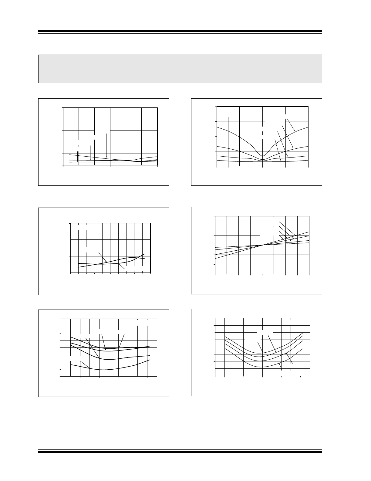
2.0 TYPICAL PERFORMANCE CURVES
Note: The graphs and tables provided following this note are a statistical summary based on a limited number of
samples and are provided for informational purposes only. The performance characteristics listed herein
are not tested or guaranteed. In some graphs or tables, the data presented may be outside the specified
operating range (e.g., outside specified power supply range) and therefore outside the warranted range.
Note: Unless otherwise indicated, TA = -40°C to +85°C, VDD = +5.0V, VSS = 0V, VIN+ = VIN- = V
.005
.004
.003
.002
.001
.000
Integral Nonlinearity (% of FSR)
PGA = 4
PGA = 1
2.5 3 3.5 4 4.5 5 5.5
PGA = 8
PGA = 2
V
(V)
DD
FIGURE 2-1: INL vs. Supply Voltage
(V
).
DD
0.003
PGA = 1
0.002
VDD = 5 V
0.001
(% of FSR)
Integral Nonlinearity
0
-60 -40 -20 0 20 40 60 80 100 120 140
Temperature (oC)
VDD = 2.7V
10.0
TA = +25°C
V
= 5V
DD
7.5
5.0
Noise (µV, rms)
2.5
0.0
-100 -75 -50 -25 0 25 50 75 100
Input Voltage (% of Full-Scale)
PGA = 8
FIGURE 2-4: Noise vs. Input Voltage.
3.0
2.0
1.0
0.0
-1.0
Total Error (mV)
-2.0
-3.0
-100 -75 -50 -25 0 25 50 75 100
Input Voltage (% of Full-Scale)
PGA = 1
PGA = 2
PGA = 4
PGA = 8
REF
PGA = 2
PGA = 4
/2.
PGA = 1
FIGURE 2-2: INL vs. Temperature.
20
15
10
5
0
-5
PGA = 1
-10
Offset Error (µV)
-15
-20
-60 -40 -20 0 20 40 60 80 100 120 140
PGA = 4
PGA = 2
Temperature (°C)
PGA = 8
VDD = 5V
FIGURE 2-3: Offset Error vs. Temperature.
FIGURE 2-5: Total Error vs. Input Voltage.
0.4
0.3
0.2
0.1
0
-0.1
-0.2
Gain Error (% of FSR)
-0.3
-0.4
-60 -40 -20 0 20 40 60 80 100 120 140
PGA = 1
PGA = 2
Temperature (°C)
VDD = 5.0V
PGA = 4
PGA = 8
FIGURE 2-6: Gain Error vs. Temperature.
DS22003B-page 4 © 2006 Microchip Technology Inc.
Page 5
MCP3421
P
Note: Unless otherwise indicated, TA = -40°C to +85°C, VDD = +5.0V, VSS = 0V, VIN+ = VIN- = V
220
200
180
(µA)
160
DDA
I
140
120
100
-60 -40 -20 0 20 40 60 80 100 120 140
FIGURE 2-7: I
600
500
400
(nA)
300
DDS
I
200
100
0
-60 -40 -20 0 20 40 60 80 100 120 140
VDD = 5V
Temperature (oC)
vs. Temperature.
DDA
VDD = 5V
Temperature (
o
VDD = 2.7V
VDD= 2.7V
C)
5
4
3
2
VDD = 2.7V
1
Oscillator Drift (%)
VDD = 5.0V
0
-1
-60 -40 -20 0 20 40 60 80 100 120 140
Temperature (°C)
FIGURE 2-10: OSC Drift vs. Temperature.
0
-10
-20
-30
-40
-50
-60
-70
-80
Magnitude (dB)
-90
-100
-110
-120
0.1 1 10 100 1000 10000
0.1 1 10 100 1k 10k
Input Signal Frequency (Hz)
/2.
REF
Data Rate = 3.75 SPS
FIGURE 2-8: I
9
8
VDD = 5V
7
VDD = 4.5V
6
A)
5
VDD = 3.3V
(
4
DDB
I
3
VDD = 2.7V
2
1
0
-60 -40 -20 0 20 40 60 80 100 120 140
FIGURE 2-9: I
vs. Temperature.
DDS
Temperature (
vs. Temperature.
DDB
FIGURE 2-11: Frequency Response.
o
C)
© 2006 Microchip Technology Inc. DS22003B-page 5
Page 6
MCP3421
3.0 PIN DESCRIPTIONS
TABLE 3-1: PIN FUNCTION TABLE
Pin No Sym Function
1V
2VSSGround Pin
3SCL
4SDA
5V
6V
+ Non-Inverting Analog Input Pin
IN
Serial Clock Input Pin of the I2C Interface
Bidirectional Serial Data Pin of the I2C Interface
DD
IN
Positive Supply Voltage Pin
- Inverting Analog Input Pin
3.1 Analog Inputs (VIN+, VIN-)
VIN+ and VIN- are differential signal input pins. The
MCP3421 device accepts a fully differential analog
input signal which is connected on the V
+ and VIN-
IN
input pins. The differential voltage that is converted is
defined by V
= (VIN+ - VIN-) where VIN+ is the voltage
IN
applied at the VIN+ pin and VIN- is the voltage applied
at the V
- pin. The input signal level is amplified by the
IN
programmable gain amplifier (PGA) before the
conversion. The differential input voltage should not
exceed an absolute of (2* V
measurement, where V
REF
/PGA) for accurate
REF
is the internal reference
voltage (2.048V) and PGA is the PGA gain setting. The
converter output code will saturate if the input range
exceeds (2* V
REF
/PGA).
The absolute voltage range on each of the differential
input pins is from V
-0.3V to VDD+0.3V. Any voltage
SS
above or below this range will cause leakage currents
through the Electrostatic Discharge (ESD) diodes at
the input pins. This ESD current can cause unexpected
performance of the device. The common mode of the
analog inputs should be chosen such that both the
differential analog input range and the absolute voltage
range on each pin are within the specified operating
range defined in Section 1.0 “Electrical
Characteristics” and Section 4.0 “Description of
Device Operation”.
3.2 Supply Voltage (VDD, VSS)
VDD is the power supply pin for the device. This pin
requires an appropriate bypass capacitor of about
0.1 µF (ceramic) to ground. An additional 10 µF
capacitor (tantalum) in parallel is also recommended
to further attenuate high frequency noise present in
some application boards. The supply voltage (V
must be maintained in the 2.7V to 5.5V range for specified operation.
is the ground pin and the current return path of the
V
SS
device. The user must connect the V
pin to a ground
SS
plane through a low impedance connection. If an
analog ground path is available in the application PCB
(printed circuit board), it is highly recommended that
DD
the V
pin be tied to the analog ground path or
SS
isolated within an analog ground plane of the circuit
board.
3.3 Serial Clock Pin (SCL)
SCL is the serial clock pin of the I2C interface. The
MCP3421 acts only as a slave and the SCL pin
accepts only external serial clocks. The input data
from the Master device is shifted into the SDA pin on
the rising edges of the SCL clock and output from the
MCP3421 occurs at the falling edges of the SCL clock.
The SCL pin is an open-drain N-channel driver.
Therefore, it needs a pull-up resistor from the V
to the SCL pin. Refer to Section 5.3 “I2C Serial Communications” for more details of I
2
C Serial Interface
DD
line
communication.
3.4 Serial Data Pin (SDA)
SDA is the serial data pin of the I2C interface. The SDA
pin is used for input and output data. In read mode, the
conversion result is read from the SDA pin (output). In
write mode, the device configuration bits are written
(input) though the SDA pin. The SDA pin is an opendrain N-channel driver. Therefore, it needs a pull-up
resistor from the V
start and stop conditions, the data on the SDA pin must
be stable during the high period of the clock. The high
or low state of the SDA pin can only change when the
clock signal on the SCL pin is low. Refer to Section 5.3
2
C Serial Communications” for more details of I2C
“I
Serial Interface communication.
)
line to the SDA pin. Except for
DD
DS22003B-page 6 © 2006 Microchip Technology Inc.
Page 7
MCP3421
4.0 DESCRIPTION OF DEVICE OPERATION
4.1 General Overview
The MCP3421 is a low-power, 18-Bit Delta-Sigma A/D
converter with an I2C serial interface. The device
contains an on-board voltage reference (2.048V),
programmable gain amplifier (PGA), and internal
oscillator. The user can select 12, 14, 16, or 18 bit
conversion by setting the configuration register bits.
The device can be operated in Continuous Conversion
or One-Shot Conversion mode. In the Continuous Conversion mode, the device converts the inputs
continuously. While in the One-Shot Conversion mode,
the device converts the input one time and stays in the
low-power standby mode until it receives another
command for a new conversion. During the standby
mode, the device consumes less than 0.1 µA typical.
4.2 Power-On-Reset (POR)
The device contains an internal Power-On-Reset
(POR) circuit that monitors power supply voltage (VDD)
during operation. This circuit ensures correct device
start-up at system power-up and power-down events.
The POR has built-in hysteresis and a timer to give a
high degree of immunity to potential ripples and noises
on the power supply. A 0.1 µF decoupling capacitor
should be mounted as close as possible to the V
for additional transient immunity.
The threshold voltage is set at 2.2V with a tolerance of
approximately ±5%. If the supply voltage falls below
this threshold, the device will be held in a reset
condition. The typical hysteresis value is approximately
200 mV.
The POR circuit is shut-down during the low-power
standby mode. Once a power-up event has occurred,
the device requires additional delay time (approximately 300 µs) before a conversion can take place.
During this time, all internal analog circuitries are
settled before the first conversion occurs. Figure 4-1
illustrates the conditions for power-up and power-down
events under typical start-up conditions.
When the device powers up, it automatically resets
and sets the configuration bits to default settings. The
default configuration bit conditions are a PGA gain of
1 V/V and a conversion speed of 240 SPS in
Continuous Conversion mode. When the device
receives an I
2
C General Call Reset command, it
performs an internal reset similar to a Power-On-Reset
event.
DD
pin
V
DD
2.2V
2.0V
300 µS
Reset
Start-up
Normal Operation
Reset
Time
FIGURE 4-1: POR Operation.
4.3 Internal Voltage Reference
The device contains an on-board 2.048V voltage
reference. This reference voltage is for internal use
only and not directly measurable. The specifications of
the reference voltage are part of the device’s gain and
drift specifications. Therefore, there is no separate
specification for the on-board reference.
4.4 Analog Input Channel
The differential analog input channel has a switched
capacitor structure. The internal sampling capacitor
(3.2 pF) is charged and discharged to process a
conversion. The charging and discharging of the input
sampling capacitor creates dynamic input currents at
the V
+ and VIN- input pins, which is inversely
IN
proportional to the internal sampling capacitor and
internal frequency. The current is also a function of the
differential input voltages. Care must be taken in setting
the common-mode voltage and input voltage ranges so
that the input limits do not exceed the ranges specified
in Section 1.0 “Electrical Characteristics”.
4.5 Digital Output Code
The digital output code produced by the MCP3421 is a
function of PGA gain, input signal, and internal
reference voltage. In a fixed setting, the digital output
code is proportional to the voltage difference between
the two analog inputs.
The output data format is a binary two’s complement.
With this code scheme, the MSB can be considered a
sign indicator. When the MSB is a logic ‘0’, it indicates
a positive value. When the MSB is a logic ‘1’, it
indicates a negative value. The following is an example
of the output code:
(a) for a negative full-scale input voltage: 100...000
(b) for a zero differential input voltage: 000...000
(c) for a positive full-scale input voltage: 011...111.
The MSB is always transmitted first through the serial
port. The number of data bits for each conversion is 18,
16, 14, or 12 bits depending on the conversion mode
selection.
© 2006 Microchip Technology Inc. DS22003B-page 7
Page 8
MCP3421
The output codes will not roll-over if the input voltage
exceeds the maximum input range. In this case, the
code will be locked at 0111...11 for all voltages
greater than +(V
voltages less than -V
of output codes of various input levels using 18 bit
conversion mode. Ta bl e 4 -3 shows an example of
minimum and maximum codes for each data rate
option.
The output code is given by:
- 1 LSB) and 1000...00 for
REF
. Ta ble 4 - 2 shows an example
REF
EQUATION 4-1:
VIN+VIN-–()
Output Code Max Code 1+()
The LSB of the code is given by:
---------------------------------------
×=
2.048V
EQUATION 4-2:
×
LSB
Where:
N = the number of bits
2 2.048V
--------------------------=
N
2
TABLE 4-1: LSB SIZE OF VARIOUS BIT
CONVERSION MODES
Bit Resolutions LSB (V)
12 bits 1 mV
14 bits 250 µV
16 bits 62.5 µV
18 bits 15.625 µV
TABLE 4-2: EXAMPLE OF OUTPUT CODE
FOR 18 BITS
Input Voltage (V) Digital Code
≥ V
REF
V
- 1 LSB 011111111111111111
REF
2LSB 000000000000000010
1LSB 000000000000000001
0 000000000000000000
-1 LSB 111111111111111111
-2 LSB 111111111111111110
- V
REF
< -V
REF
011111111111111111
100000000000000000
100000000000000000
TABLE 4-3: MINIMUM AND MAXIMUM
CODES
Number
of Bits
12 240 SPS -2048 2047
14 60 SPS -8192 8191
16 15 SPS -32768 32767
18 3.75 SPS -131072 131071
Note: Maximum n-bit code = 2
Data Rate
Minimum n-bit code = -1 x 2
Minimum
Code
n-1
- 1
Maximum
Code
n-1
4.6 Self-Calibration
The device performs a self-calibration of offset and
gain for each conversion. This provides reliable
conversion results from conversion-to-conversion over
variations in temperature as well as power supply
fluctuations.
4.7 Input Impedance
The MCP3421 uses a switched-capacitor input stage
using a 3.2 pF sampling capacitor. This capacitor is
switched (charged and discharged) at a rate of the
sampling frequency that is generated by the on-board
clock. The differential mode impedance varies with the
PGA settings. The typical differential input impedance
during a normal mode operation is given by:
ZIN(f) = 2.25 MΩ/PGA
Since the sampling capacitor is only switching to the
input pins during a conversion process, the above input
impedance is only valid during conversion periods. In a
low power standby mode, the above impedance is not
presented at the input pins. Therefore, only a leakage
current due to ESD diode is presented at the input pins.
The conversion accuracy can be affected by the input
signal source impedance when any external circuit is
connected to the input pins. The source impedance
adds to the internal impedance and directly affects the
time required to charge the internal sampling capacitor.
Therefore, a large input source impedance connected
to the input pins can increase the system performance
errors such as offset, gain, and integral nonlinearity
(INL) errors. Ideally, the input source impedance
should be zero. This can be achievable by using an
operational amplifier with a closed-loop output
impedance of tens of ohms.
DS22003B-page 8 © 2006 Microchip Technology Inc.
Page 9

4.8 Aliasing and Anti-aliasing Filter
Aliasing occurs when the input signal contains timevarying signal components with frequency greater than
half the sample rate. In the aliasing conditions, the
device can output unexpected output codes. For
applications that are operating in electrical noise
environments, the time-varying signal noise or high
frequency interference components can be easily
added to the input signals and cause aliasing. Although
the MCP3421 device has an internal first order sinc
filter, its’ filter response may not give enough
attenuation to all aliasing signal components. To avoid
the aliasing, an external anti-aliasing filter, which can
be accomplished with a simple RC low-pass filter, is
typically used at the input pins. The low-pass filter cuts
off the high frequency noise components and provides
a band-limited input signal to the MCP3421 input pins.
MCP3421
© 2006 Microchip Technology Inc. DS22003B-page 9
Page 10

MCP3421
5.0 USING THE MCP3421 DEVICE
5.1 Operating Modes
The user operates the device by setting up the device
configuration register and reads the conversion data
using serial I2C interface commands. The MCP3421
operates in two modes: (a) Continuous Conversion
Mode or (b) One-Shot Conversion Mode (single
conversion). The selection is made by setting the O
bit in the Configuration Register. Refer to Section 5.2
“Configuration Register” for more information.
5.1.1 CONTINUOUS CONVERSION
MODE (O
The MCP3421 device performs a Continuous
Conversion if the O
conversion is completed, the result is placed at the
output data register. The device immediately begins
another conversion and overwrites the output data
register with the most recent data.
The device also clears the data ready flag (RDY
when the conversion is completed. The device sets the
ready flag bit (RDY
result has been read by the Master.
/C BIT = 1)
/C bit is set to logic “high”. Once the
bit = 1), if the latest conversion
/C
bit = 0)
5.1.2 ONE-SHOT CONVERSION MODE
(O
/C BIT = 0)
Once the One-Shot Conversion (single conversion)
Mode is selected, the device performs a conversion,
updates the Output Data register, clears the data ready
flag (RDY
mode. A new One-Shot Conversion is started again
when the device receives a new write command with
RDY
This One-Shot Conversion Mode is recommended for
low power operating applications. During the low
current standby mode, the device consumes less than
1 µA typical. For example, if user collects 18 bit
conversion data once a second in One-Shot Conversion mode, the device draws only about one fourth of
its total operating current. In this example, the device
consumes approximately 39 µA (= ~145 µA/3.75 SPS),
if the device performs only one conversion per second
(1 SPS) in 18-bit conversion mode with 3V power
supply.
= 0), and then enters a low power standby
= 1.
DS22003B-page 10 © 2006 Microchip Technology Inc.
Page 11

MCP3421
5.2 Configuration Register
The MCP3421 has an 8-bit wide configuration register
to select for: PGA gain, conversion rate, and conversion mode. This register allows the user to change the
operating condition of the device and check the status
of the device operation. The user can rewrite the
configuration byte any time during the device
operation. Register 5-1 shows the configuration
register bits.
REGISTER 5-1: CONFIGURATION REGISTER
R/W-1 R/W-0 R/W-0 R/W-1 R/W-0 R/W-0 R/W-0 R/W-0
RDY C1 C0 O/C S1 S0 G1 G0
1 * 0 * 0 * 1 * 0 * 0 * 0 * 0 *
bit 7 bit 0
* Default Configuration after Power-On Reset
Legend:
R = Readable bit W = Writable bit U = Unimplemented bit, read as ‘0’
-n = Value at POR ‘1’ = Bit is set ‘0’ = Bit is cleared x = Bit is unknown
bit 7 RDY
bit 6-5 C1-C0: Channel Selection Bits
bit 4 O
bit 3-2 S1-S0: Sample Rate Selection Bit
bit 1-0 G1-G0: PGA Gain Selector Bits
: Ready Bit
This bit is the data ready flag. In read mode, this bit indicates if the output register has been updated
with a new conversion. In One-Shot Conversion mode, writing this bit to “1” initiates a new conversion.
Reading RDY bit with the read command:
1 = Output register has not been updated.
0 = Output register has been updated with the latest conversion data.
Writing
Continuous Conversion mode: No effect
One-Shot Conversion mode:
1 = Initiate a new conversion.
0 = No effect.
These are the Channel Selection bits, but not used in the MCP3421 device.
1 = Continuous Conversion Mode. Once this bit is selected, the device performs data conversions
0 = One-Shot Conversion Mode. The device performs a single conversion and enters a low power
00 = 240 SPS (12 bits),
01 = 60 SPS (14 bits),
10 = 15 SPS (16 bits),
11 = 3.75 SPS (18 bits)
00 = 1 V/V,
01 = 2 V/V,
10 = 4 V/V,
11 = 8 V/V
RDY bit with the write command:
/C: Conversion Mode Bit
continuously.
standby mode until it receives another write/read command.
© 2006 Microchip Technology Inc. DS22003B-page 11
Page 12

MCP3421
In read mode, the RDY bit in the configuration byte
indicates the state of the conversion: (a) RDY = 1
indicates that the data bytes that have just been read
were not updated from the previous conversion. (b)
= 0 indicates that the data bytes that have just
RDY
been read were updated.
If the configuration byte is read repeatedly by clocking
continuously after the first read (i.e., after the 5th byte
in the 18-bit conversion mode), the state of the RDY
indicates whether the device is ready with new
conversion data. See Figure 5-2. For example,
= 0 means new conversion data is ready for read-
RDY
ing. In this case, the user can send a stop bit to exit the
current read operation and send a new read command
to read out updated conversion data. See Figures 5-2
and 5-3 for reading conversion data. The user can
rewrite the configuration byte any time for a new
setting. Tables 5-1 and 5-2 show the examples of the
configuration bit operation.
TABLE 5-1: CONFIGURATION BITS FOR
bit
WRITING
R/W O/C RDY Operation
0 0 0 No effect if all other bits remain
the same - operation continues
with the previous settings
0 0 1 Initiate One-Shot Conversion
0 1 0 Initiate Continuous Conversion
0 1 1 Initiate Continuous Conversion
TABLE 5-2: CONFIGURATION BITS FOR
READING
R/W O/C RDY Operation
1 0 0 New conversion data in One-
Shot conversion mode has been
just read. The RDY
low until set by a new write
command.
1 0 1 One-Shot Conversion is in
progress, The conversion data is
not updated yet. The RDY
stays high.
1 1 0 New conversion data in Continu-
ous Conversion mode has been
just read. The RDY
to high after this read.
1 1 1 The conversion data in Continu-
ous Conversion mode was
already read. The latest conver-
sion data is not ready. The RDY
bit stays high until a new
conversion is completed.
bit remains
bit
bit changes
5.3 I2C Serial Communications
The MCP3421 device communicates with Master
(microcontroller) through a serial I
Circuit) interface and supports standard
(100 kbits/sec), fast (400 kbits/sec) and high-speed
(3.4 Mbits/sec) modes. The serial I
2-wire data bus communication protocol using opendrain SCL and SDA lines.
The MCP3421 can only be addressed as a slave. Once
addressed, it can receive configuration bits or transmit
the latest conversion results. The serial clock pin (SCL)
is an input only and the serial data pin (SDA) is
bidirectional. An example of a hardware connection
diagram is shown in Figure 6-1.
The Master starts communication by sending a START
bit and terminates the communication by sending a
STOP bit. The first byte after the START bit is always
the address byte of the device, which includes the
device code, the address bits, and the R/W
device code for the MCP3421 device is 1101. The
address bits (A2, A1, A0) are pre-programmed at the
factory. In general, the address bits are specified by the
customer when they order the device. The three
address bits are programmed to “000” at the factory, if
they are not specified by the customer. Figure 5-1
shows the details of the MCP3421 address byte.
During a low power standby mode, SDA and SCL pins
remain at a floating condition.
2
More details of the I
in Section 5.6 “I
C bus characteristic is described
2
C Bus Characteristics”.
5.3.1 DEVICE ADDRESSING
The address byte is the first byte received following the
START condition from the Master device. The
MCP3421 device code is 1101. The device code is
followed by three address bits (A2, A1, A0) which are
programmed at the factory. The three address bits
allow up to eight MCP3421 devices on the same data
bus line. The (R/W
wants to read the conversion data or write to the
Configuration register. If the (R/W
mode), the MCP3421 outputs the conversion data in
the following clocks. If the (R/W
mode), the MCP3421 expects a configuration byte in
the following clocks. When the MCP3421 receives the
correct address byte, it outputs an acknowledge bit
after the R/W
address byte. See Figures 5-2 and 5-3 for the read and
write operations of the device.
) bit determines if the Master device
bit. Figure 5-1 shows the MCP3421
2
C (Inter-Integrated
2
C is a bidirectional
bit. The
) bit is set (read
) bit is cleared (write
DS22003B-page 12 © 2006 Microchip Technology Inc.
Page 13

MCP3421
Acknowledge bit
Start bit
Address
Address Byte
Address
Device Code Address Bits
1
Note 1: Specified by customer and programmed at the
0
1
factory. If not specified by the customer,
programmed to ‘
1
X
000’.
Read/Write
X
bit
(Note 1)
X
R/W
ACK
FIGURE 5-1: MCP3421 Address Byte.
5.3.2 READING DATA FROM THE DEVICE
When the Master sends a read command (R/W = 1),
the MCP3421 outputs the conversion data bytes and
configuration byte. Each byte consists of 8 bits with
one acknowledge (ACK) bit. The ACK bit after the
address byte is issued by the MCP3421 and the ACK
bits after each conversion data bytes are issued by the
Master.
When the device is configured for 18-bit conversion
mode, the device outputs three data bytes followed by
a configuration byte. The first 7 data bits in the first
data byte are the MSB of the conversion data. The
user can ignore the first 6 data bits, and take the 7th
data bit (D17) as the MSB of the conversion data. The
LSB of the 3rd data byte is the LSB of the conversion
data (D0).
If the device is configured for 12, 14, or 16 bit-mode, the
device outputs two data bytes followed by a
configuration byte. In 16 bit-conversion mode, the MSB
of the first data byte is the MSB (D15) of the conversion
data. In 14-bit conversion mode, the first two bits in the
first data byte can be ignored (they are the MSB of the
conversion data), and the 3rd bit (D13) is the MSB of
the conversion data. In 12-bit conversion mode, the
first four bits can be ignored (they are the MSB of the
conversion data), and the 5th bit (D11) of the byte
represents the MSB of the conversion data. Table 5-3
shows an example of the conversion data output of
each conversion mode.
The configuration byte follows the output data byte.
The device outputs the configuration byte as long as
the SCL pulses are received. The device terminates
the current outputs when it receives a Not-Acknowledge (NAK), a repeated start or a stop bit at any time
during the output bit stream. It is not required to read
the configuration byte. However, the user may read the
configuration byte to check the RDY
bit condition to
confirm whether the just received data bytes are
updated conversion data. The user may continuously
send clock (SCL) to repeatedly read the configuration
bytes to check the RDY
bit status.
Figures 5-2 and 5-3 show the timing diagrams of the
reading.
5.3.3 WRITING A CONFIGURATION BYTE
TO THE DEVICE
When the Master sends an address byte with the R/W
bit low (R/W = 0), the MCP3421 expects one
configuration byte following the address. Any byte sent
after this second byte will be ignored. The user can
change the operating mode of the device by writing the
configuration register bits.
If the device receives a write command with a new
configuration setting, the device immediately begins a
new conversion and updates the conversion data.
TABLE 5-3: EXAMPLE OF CONVERSION DATA OUTPUT OF EACH CONVERSION MODE
Conversion
Mode
18-bits MMMMMMMD16 (1st data byte) - D15 ~ D8 (2nd data byte) - D7 ~ D0 (3rd data byte) - Configuration
byte
16-bits MD14~D8 (1st data byte) - D7 ~ D0 (2nd data byte) - Configuration byte
14-bits MMMD12~D8 (1st data byte) - D7 ~ D0 (2nd data byte) - Configuration byte
12-bits MMMMMD10D9D8 (1st data byte) - D7 ~ D0 (2nd data byte) - Configuration byte
Note: M is MSB of the data byte.
© 2006 Microchip Technology Inc. DS22003B-page 13
Conversion Data Output
Page 14

MCP3421
9
G
G
S
S
C
C
1
D
D
D
D
D
D
D
D
9
D
D
D
D
D
D
D
191
9
7
D
D
D
Master
ACK by
0
1
0
1
O/C
5th Byte
0
1
RDY
Master
ACK by
0
1
2
3
4
5
6
7
Master
ACK by
8
9
10
11
12
13
14
15
Master
ACK by
16
17
Configuration Byte
4th Byte
Lower Data Byte
3rd Byte
Middle Data Byte
(Optional)
Master
9
1
Stop Bit by
0
G
G
S
S
C
C
Master
NAK by
1
0
1
O/C
0
1
RDY
(Optional)
Configuration Byte
Nth Repeated Byte:
2nd Byte
can be ignored)
Upper Data Byte
(Data on Clocks 1-6th
1
9
1
SCL
Repeat of D17 (MSB)
ACK by
MCP3421
R/W
1st Byte
Start Bit by
MCP3421 Address Byte
– Address Bits A2- A0 = 000 are programmed at the factory unless customer requests specific codes.
– Stop bit or NAK bit can be issued any time during reading.
– Data bits on clocks 1 - 6th in 2nd byte are repeated MSB and can be ignored.
Master
Note: – MCP3421 device code is 1101.
1 1 0 1 A2 A1 A0
SDA
FIGURE 5-2: Timing Diagram For Reading From The MCP3421 With 18-Bit Mode.
DS22003B-page 14 © 2006 Microchip Technology Inc.
Page 15

MCP3421
9
G
G
S
S
C
C
1
9
D
D
D
D
D
D
D
1
1
99
9
D
D
D
D
D
D
D
D
D
Master
ACK by
0
1
0
1
0
1
0
1
2
3
4
5
6
7
8
9
10
11
12
13
14
15
O/C
RDY
Master
ACK by
Master
ACK by
ACK by
MCP3421
4th Byte
(Optional)
Configuration Byte
9
G
G
S
S
3rd Byte
Lower Data Byte
1
2nd Byte
Middle Data Byte
C
C
Master
Stop Bit by
0
Master
NAK by
1
0
1
O/C
0
1
RDY
(Optional)
Configuration Byte
Nth Repeated Byte:
R/W
1st Byte
MCP3421 Address Byte
1
SCL
1101A2A1A0
SDA
Start Bit by
– Address Bits A2- A0 = 000 are programmed at the factory unless customer requests specific codes.
– Stop bit or NAK bit can be issued any time during reading.
– In 14 - bit mode: D15 and D14 are repeated MSB and can be ignored.
– In 12 - bit mode: D15 - D12 are repeated MSB and can be ignored.
Master
Note: – MCP3421 device code is 1101.
FIGURE 5-3: Timing Diagram For Reading From The MCP3421 With 12-Bit to 16-Bit Modes.
© 2006 Microchip Technology Inc. DS22003B-page 15
Page 16

MCP3421
1
SCL
1
9
9
SDA
Start Bit by
Master
1101A2A1
R/W
A0
ACK by
MCP3421
C1 C0
RDY
O/C
1st Byte:
MCP3421 Address Byte
with Write command
2nd Byte:
Configuration Byte
Note: – Stop bit can be issued any time during writing.
– MCP3421 device code is 1101.
– Address Bits A2- A0 = 000 are programmed at factory unless customer requests different codes.
FIGURE 5-4: Timing Diagram For Writing To The MCP3421.
5.4 General Call
The MCP3421 acknowledges the general call address
(0x00 in the first byte). The meaning of the general call
address is always specified in the second byte. Refer
0
to Figure 5-5. The MCP3421 supports the following
general calls:
5.4.1 GENERAL CALL RESET
The general call reset occurs if the second byte is
‘00000110’ (06h). At the acknowledgement of this
byte, the device will abort current conversion and
perform an internal reset similar to a power-on-reset
(POR).
5.4.2 GENERAL CALL CONVERSION
The general call conversion occurs if the second byte
is ‘00001000’ (08h). All devices on the bus initiate a
conversion simultaneously. For the MCP3421 device,
the configuration will be set to the One-Shot Conversion mode and a single conversion will be performed.
The PGA and data rate settings are unchanged with
this general call.
Note: The I2C specification does not allow to use
“00000000” (00h) in the second byte.
0 0 0 0 0 0 0
(General Call Address)
FIGURE 5-5: General Call Address Format.
For more information on the general call, or other I2C
modes, please refer to the Phillips I
S1 S0 G1 G0
ACK by
MCP3421
First Byte
Stop Bit by
Master
ACK
x
A Axxxxxx x
Second Byte
2
C specification.
ACK
LSB
DS22003B-page 16 © 2006 Microchip Technology Inc.
Page 17

MCP3421
5.5 High-Speed (HS) Mode
The I2C specification requires that a high-speed mode
device must be ‘activated’ to operate in high-speed
mode. This is done by sending a special address byte
of 00001XXX following the START bit. The XXX bits are
unique to the High-Speed (HS) mode Master. This byte
is referred to as the High-Speed (HS) Master Mode
Code (HSMMC). The MCP3421 device does not
acknowledge this byte. However, upon receiving this
code, the MCP3421 switches on its HS mode filters
and communicates up to 3.4 MHz on SDA and SCL.
The device will switch out of the HS mode on the next
STOP condition.
For more information on the HS mode, or other I
modes, please refer to the Phillips I
2
C specification.
2
5.6 I2C Bus Characteristics
The I2C specification defines the following bus
protocol:
• Data transfer may be initiated only when the bus
is not busy.
• During data transfer, the data line must remain
stable whenever the clock line is HIGH. Changes
in the data line while the clock line is HIGH will be
interpreted as a START or STOP condition.
Accordingly, the following bus conditions have been
defined using Figure 5-6.
5.6.1 BUS NOT BUSY (A)
Both data and clock lines remain HIGH.
5.6.2 START DATA TRANSFER (B)
A HIGH to LOW transition of the SDA line while the
clock (SCL) is HIGH determines a START condition. All
commands must be preceded by a START condition.
5.6.3 STOP DATA TRANSFER (C)
A LOW to HIGH transition of the SDA line while the
clock (SCL) is HIGH determines a STOP condition. All
operations can be ended with a STOP condition.
5.6.4 DATA VALID (D)
The state of the data line represents valid data when,
after a START condition, the data line is stable for the
duration of the HIGH period of the clock signal.
The data on the line must be changed during the LOW
period of the clock signal. There is one clock pulse per
bit of data.
Each data transfer is initiated with a START condition
and terminated with a STOP condition.
5.6.5 ACKNOWLEDGE
The Master (microcontroller) and the slave (MCP3421)
C
use an acknowledge pulse as a hand shake of
communication for each byte. The ninth clock pulse of
each byte is used for the acknowledgement. The
acknowledgement is achieved by pulling-down the
SDA line “LOW” during the 9th clock pulse. The clock
pulse is always provided by the Master (microcontroller) and the acknowledgement is issued by the
receiving device of the byte (Note: The transmitting
device must release the SDA line (“HIGH”) during the
acknowledge pulse.). For example, the slave
(MCP3421) issues the acknowledgement (bring down
the SDA line “LOW”) after the end of each receiving
byte, and the master (microcontroller) issues the
acknowledgement when it reads data from the Slave
(MCP3421).
When the MCP3421 is addressed, it generates an
acknowledge after receiving each byte successfully.
The Master device (microcontroller) must provide an
extra clock pulse (9th pulse of each byte) for the
acknowledgement from the MCP3421 (slave).
The MCP3421 (slave) pulls-down the SDA line during
the acknowledge clock pulse in such a way that the
SDA line is stable low during the high period of the
acknowledge clock pulse.
During reads, the Master (microcontroller) can
terminate the current read operation by not providing
an acknowledge bit on the last byte that has been
clocked out from the MCP3421. In this case, the
MCP3421 releases the SDA line to allow the master
(microcontroller) to generate a STOP or repeated
START condition.
(A) (B) (D) (D) (A)(C)
SCL
SDA
START
CONDITION
ADDRESS OR
ACKNOWLEDGE
VAL ID
DATA
ALLOWED
TO CHANGE
STOP
CONDITION
FIGURE 5-6: Data Transfer Sequence on the Serial Bus.
© 2006 Microchip Technology Inc. DS22003B-page 17
Page 18

MCP3421
TABLE 5-4: I2C SERIAL TIMING SPECIFICATIONS
Electrical Specifications: Unless otherwise specified, all limits are specified for TA = -40 to +85°C, VDD = +2.7V, +3.3V or +5.0V,
V
= 0V, VIN+ = VIN- = V
SS
Parameters Sym Min Typ Max Units Conditions
Standard Mode
Clock frequency f
Clock high time
Clock low time
SDA and SCL rise time
SDA and SCL fall time
START condition hold time T
Repeated START condition
setup time
Data hold time
(Note 3)
Data input setup time
STOP condition setup time
STOP condition hold time
Output valid from clock
(Notes 2 and 3)
Bus free time
Fast Mode
Clock frequency
Clock high time
Clock low time
SDA and SCL rise time
SDA and SCL fall time
START condition hold time T
Repeated START condition
setup time
Data hold time
(Note 4)
Data input setup time
STOP condition setup time
STOP condition hold time
Output valid from clock
(Notes 2 and 3)
Bus free time
Input filter spike suppression
(Note 5)
Note 1: This parameter is ensured by characterization and not 100% tested.
2: This specification is not a part of the I
plus SDA Fall (or rise) time:
3: If this parameter is too short, it can create an unintended Start or Stop condition to other devices on the bus line. If this
parameter is too long, Clock Low time (T
4: For Data Input: This parameter must be longer than t
Clock Low time (T
For Data Output: This parameter is characterized, and tested indirectly by testing T
5: This parameter is ensured by characterization and not 100% tested. This parameter is not available for Standard Mode.
REF
(Note 1)
(Note 1)
(Note 1)
(Note 1)
/2.
SCL
T
HIGH
T
LOW
T
R
T
F
HD:STA
T
SU:STA
T
HD:DAT
T
SU:DAT
T
SU:STO
T
HD:STD
T
AA
T
BUF
T
SCL
T
HIGH
T
LOW
T
R
T
F
HD:STA
T
SU:STA
T
HD:DAT
T
SU:DAT
T
SU:STO
T
HD:STD
T
AA
T
BUF
T
SP
T
) can be affected.
LOW
0 — 100 kHz
4000 — — ns
4700 — — ns
— — 1000 ns From VIL to V
— — 300 ns From VIH to V
4000 — — ns After this period, the first clock
pulse is generated.
4700 — — ns Only relevant for repeated Start
condition
0 — 3450 ns
250 — — ns
4000 — — ns
4000 — — ns
0 — 3750 ns
4700 — — ns Time between START and STOP
conditions.
0 — 400 kHz
600 — — ns
1300 — — ns
20 + 0.1Cb — 300 ns From VIL to V
20 + 0.1Cb — 300 ns From VIH to V
600 — — ns After this period, the first clock
pulse is generated
600 — — ns Only relevant for repeated Start
condition
0 — 900 ns
100 — — ns
600 — — ns
600 — — ns
0 — 1200 ns
1300 — — ns Time between START and STOP
conditions.
0 — 50 ns SDA and SCL pins
2
C specification. This specification is equivalent to the Data Hold Time (T
AA
= T
HD:DAT
LOW
+ TF (OR TR).
) can be affected.
. If this parameter is too long, the Data Input Setup (T
SP
parameter.
AA
IH
IL
IH
IL
HD:DAT
SU:DAT
)
) or
DS22003B-page 18 © 2006 Microchip Technology Inc.
Page 19

MCP3421
TABLE 5-4: I2C SERIAL TIMING SPECIFICATIONS (CONTINUED)
Electrical Specifications: Unless otherwise specified, all limits are specified for TA = -40 to +85°C, VDD = +2.7V, +3.3V or +5.0V,
V
= 0V, VIN+ = VIN- = V
SS
Parameters Sym Min Typ Max Units Conditions
High Speed Mode
Clock frequency f
Clock high time
Clock low time
SCL rise time
SCL fall time
SDA rise time
SDA fall time
(Note 1)
(Note 1)
(Note 1)
(Note 1)
START condition hold time
Repeated START condition
setup time
Data hold time
(Note 4)
Data input setup time
STOP condition setup time
STOP condition hold time
Output valid from clock
(Notes 2 and 3)
Bus free time
Input filter spike suppression
(Note 5)
Note 1: This parameter is ensured by characterization and not 100% tested.
2: This specification is not a part of the I
plus SDA Fall (or rise) time:
3: If this parameter is too short, it can create an unintended Start or Stop condition to other devices on the bus line. If this
parameter is too long, Clock Low time (T
4: For Data Input: This parameter must be longer than t
Clock Low time (T
For Data Output: This parameter is characterized, and tested indirectly by testing T
5: This parameter is ensured by characterization and not 100% tested. This parameter is not available for Standard Mode.
/2.
REF
) can be affected.
LOW
SCL
T
HIGH
T
LOW
T
T
T
R: DAT
T
F: DATA
T
HD:STA
T
SU:STA
T
HD:DAT
T
SU:DAT
T
SU:STO
T
HD:STD
T
T
BUF
T
AA
SP
0—3.4
1.7
60
——ns
120
160
——nsC
320
R
F
——4080ns From VIL to VIH,Cb = 100 pF
——4080ns From VIH to VIL,Cb = 100 pF
——80
160
——80
160
MHz
Cb = 100 pF
MHz
C
= 400 pF
b
Cb = 100 pF
ns
C
= 400 pF
b
= 100 pF
b
C
= 400 pF
b
C
= 400 pF
b
C
= 400 pF
b
ns From VIL to VIH,Cb = 100 pF
C
= 400 pF
b
ns From VIH to VIL,Cb = 100 pF
C
= 400 pF
b
160 — — ns After this period, the first clock
pulse is generated
160 — — ns Only relevant for repeated Start
condition
0
0
—70
150
ns Cb = 100 pF
C
= 400 pF
b
10 — — ns
160 — — ns
160 — — ns
— — 150
310
ns Cb = 100 pF
C
= 400 pF
b
160 — — ns Time between START and STOP
conditions.
0 — 10 ns SDA and SCL pins
2
C specification. This specification is equivalent to the Data Hold Time (T
T
AA
= T
HD:DAT
LOW
+ TF (OR TR).
) can be affected.
. If this parameter is too long, the Data Input Setup (T
SP
parameter.
AA
HD:DAT
SU:DAT
)
) or
© 2006 Microchip Technology Inc. DS22003B-page 19
Page 20

MCP3421
T
F
T
T
SU:STA
SP
T
HD:STA
T
LOW
SCL
SDA
FIGURE 5-7: I2C Bus Timing Data.
T
HIGH
T
HD:DAT
T
R
T
T
SU:DAT
T
AA
SU:STO
T
BUF
DS22003B-page 20 © 2006 Microchip Technology Inc.
Page 21

MCP3421
6.0 BASIC APPLICATION
CONFIGURATION
The MCP3421 device can be used for various precision
analog-to-digital converter applications. The device
operates with very simple connections to the
application circuit. The following sections discuss the
examples of the device connections and applications.
6.1 Connecting to the Application
Circuits
6.1.1 INPUT VOLTAGE RANGE
The fully differential input signals can be connected to
+ and VIN- input pins. The input range should be
the V
IN
within absolute common mode input voltage range:
VSS- 0.3V to VDD + 0.3V. Outside this limit, the ESD
protection diode at the input pin begins to conduct and
the error due to input leakage current increases rapidly.
Within this limit, the differential input V
is boosted by the PGA before a conversion takes place.
The MCP3421 can not accept negative input voltages
on the input pins. Figures 6-1 and 6-2 show typical connection examples for differential inputs and a singleended input, respectively. For the single-ended input,
the input signal is applied
(typically connected to the V
to one of the input pins
+ pin) while the other
IN
input pin (typically VIN- pin) is grounded. The input
signal range of the single-ended configuration is from
0V to 2.048V. All device characteristics hold for the
single-ended configuration, but this configuration loses
one bit resolution because the input can only stand in
positive half scale.
Characteristics”
.
Refer to
Section 1.0 “Electrical
6.1.2 BYPASS CAPACITORS ON VDD PIN
For accurate measurement, the application circuit
needs a clean supply voltage and must block any noise
signal to the MCP3421 device. Figure 6-1 shows an
example of using two bypass capacitors (a 10 µF
tantalum capacitor and a 0.1 µF ceramic capacitor) in
parallel on the V
line. These capacitors are helpful to
DD
filter out any high frequency noises on the V
also provide the momentary bursts of extra currents
when the device needs from the supply. These
capacitors should be placed as close to the V
possible (within one inch). If the application circuit has
separate digital and analog power supplies, the V
and VSS of the MCP3421 should reside on the analog
plane.
6.1.3 CONNECTING TO I2C BUS USING
PULL-UP RESISTORS
The SCL and SDA pins of the MCP3421 are open-drain
configurations. These pins require a pull-up resistor as
shown in Figure 6-1. The value of these pull-up resistors depends on the operating speed (standard, fast,
and high speed) and loading capacitance of the I
(= VIN+-VIN-)
IN
line and
DD
DD
pin as
DD
2
C bus
line. Higher value of pull-up resistor consumes less
power, but increases the signal transition time (higher
RC time constant) on the bus. Therefore, it can limit the
bus operating speed. The lower value of resistor, on the
other hand, consumes higher power, but allows higher
operating speed. If the bus line has higher capacitance
due to long bus line or high number of devices
connected to the bus, a smaller pull-up resistor is
needed to compensate the long RC time constant. The
pull-up resistor is typically chosen between 1 kΩ and
10 kΩ ranges for standard and fast modes, and less
than 1 kΩ for high speed mode in high loading
capacitance environments.
V
Input Signals
MCP3421
-
V
V
SDL
IN
DD
6
5
4
V
+
1
IN
V
2
SS
3
SCL
Note: R is the pull-up resistor.
DD
V
DD
R
10 µF0.1 µF
R
TO MCU
(MASTER)
FIGURE 6-1: Typical Connection Example for Differential Inputs.
V
Input Signals
MCP3421
-
V
V
SDL
IN
DD
6
5
4
+
V
1
IN
V
2
SS
3
SCL
Note: R is the pull-up resistor.
DD
V
DD
R
10 µF0.1 µF
R
TO MCU
(MASTER)
FIGURE 6-2: Typical Connection Example for Single-Ended Input.
The number of devices connected to the bus is limited
only by the maximum bus capacitance of 400 pF. The
bus loading capacitance affects on the bus operating
speed. For example, the highest bus operating speed
for the 400 pF bus capacitance is 1.7 MHz, and
3.4 MHz for 100 pF. Figure 6-3 shows an example of
multiple device connections.
© 2006 Microchip Technology Inc. DS22003B-page 21
Page 22

MCP3421
Microcontroller
(PIC16F876)
MCP3421
SDA SCL
EEPROM
(24LC01)
NPP301
V
DD
V
DD
V
DD
Temperature
Sensor
(TC74)
FIGURE 6-3: Example of Multiple Device
Connection on I
2
C Bus.
6.2 Device Connection Test
The user can test the presence of the MCP3421 on the
I2C bus line without performing an input data conversion. This test can be achieved by checking an
acknowledge response from the MCP3421 after sending a read or write command. Here is an example using
Figure 6-4:
(a) Set the R/W
(b) The MCP3421 will then acknowledge by pulling
SDA bus LOW during the ACK clock and then release
the bus back to the I
(c) A STOP or repeated START bit can then be issued
from the Master and I
bit “HIGH” in the address byte.
2
C Master.
2
C communication can continue.
Address Byte
MCP3421
-
V
V
+
1
IN
V
2
SS
3
SCL SDL
6
IN
V
5
DD
4
R
10 µF0.1 µF
R
TO MCU
(MASTER)
FIGURE 6-5: Example of Pressure Measurement.
In this circuit example, the sensor full scale range is
±7.5 mV with a common mode input voltage of V
This configuration will provide a full 14-bit resolution
across the sensor output range. The alternative circuit
for this amount of accuracy would involve an analog
gain stage prior to a 16-bit ADC.
Figure 6-6 shows an example of temperature measure-
ment using a thermistor. This example can achieve a
linear response over a 50°C temperature range. This
can be implemented using a standard resistor with 1%
tolerance in series with the thermistor. The value of the
resistor is selected to be equal to the thermistor value
at the mid-point of the desired temperature range.
DD
/ 2.
SCL
SDA
123456789
1
Start
Bit
1
Device bits
1A2A1A0
0
Address bits
1
R/W
ACK
Start
Bit
10 kΩ
Resistor
10 kΩ
Thermistor
V
DD
V
DD
V
DD
MCP3421
Response
FIGURE 6-4: I2C Bus Connection Test.
6.3 Application Examples
V
1
V
2
3
SCL
MCP3421
+
IN
SS
V
V
SDL
IN
DD
-
6
5
4
R
10 µF0.1 µF
R
The MCP3421 device can be used in a broad range of
sensor and data acquisition applications. Figure 6-5,
shows an example of interfacing with a bridge sensor
for pressure measurement.
TO MCU
(MASTER)
FIGURE 6-6: Example of Temperature Measurement.
DS22003B-page 22 © 2006 Microchip Technology Inc.
Page 23

7.0 PACKAGING INFORMATION
7.1 Package Marking Information
MCP3421
6-Lead SOT-23
5
XXNN
64
Example
2
13
5
CA25
64
2
13
Legend: XX...X Customer-specific information
Y Year code (last digit of calendar year)
YY Year code (last 2 digits of calendar year)
WW Week code (week of January 1 is week ‘01’)
NNN Alphanumeric traceability code
3
e
Pb-free JEDEC designator for Matte Tin (Sn)
* This package is Pb-free. The Pb-free JEDEC designator ( )
can be found on the outer packaging for this package.
Note: In the event the full Microchip part number cannot be marked on one line, it will
be carried over to the next line, thus limiting the number of available
characters for customer-specific information.
© 2006 Microchip Technology Inc. DS22003B-page 23
3
e
Page 24

MCP3421
6-Lead Plastic Small Outline Transistor (OT) (SOT-23)
Note: For the most current package drawings, please see the Microchip Packaging Specification located at
http://www.microchip.com/packaging
E
E1
B
n
c
β
Number of Pins
Pitch
Outside lead pitch
Foot Angle
Lead Thickness
Mold Draft Angle Top
Mold Draft Angle Bottom
*
Controlling Parameter
Notes:
Dimensions D and E1 do not include mold flash or protrusions. Mold flash or protrusions shall not exceed .005" (0.127mm) per side.
BSC: Basic Dimension. Theoretically exact value shown without tolerances.
See ASME Y14.5M
JEITA (formerly EIAJ) equivalent: SC-74A
Drawing No. C04-120
L
Units
n
p
p1
φ
c
α
β
p1
D
1
α
φ
A
A1
A2
*
MILLIMETERSINCHES
MAXNOMMINMAXNOMMINDimension Limits
66
0.95 BSC.038 BSC
1.90 BSC.075 BSC
1.451.180.90.057.046.035AOverall Height
1.301.100.90.051.043.035A2Molded Package Thickness
0.150.080.00.006.003.000A1Standoff
3.002.802.60.118.110.102EOverall Width
1.751.631.50.069.064.059E1Molded Package Width
3.102.952.80.122.116.110DOverall Length
0.550.450.35.022.018.014LFoot Length
10501050
0.200.150.09.008.006.004
0.500.430.35.020.017.014BLead Width
10501050
10501050
Revised 09-12-05
DS22003B-page 24 © 2006 Microchip Technology Inc.
Page 25

APPENDIX A: REVISION HISTORY
Revision B (December 2006)
• Changes to Electrical Characteristics tables
• Added characterization data
• Changes to I
• Change to Figure 5-7.
Revision A (August 2006)
• Original Release of this Document.
2
C Serial Timing Specification table
MCP3421
© 2006 Microchip Technology Inc. DS22003B-page 27
Page 26

MCP3421
NOTES:
DS22003B-page 28 © 2006 Microchip Technology Inc.
Page 27

PRODUCT IDENTIFICATION SYSTEM
To order or obtain information, e.g., on pricing or delivery, refer to the factory or the listed sales office.
PART NO. XXX
Device
Device: MCP3421T: Single Channel ΔΣ A/D Converter
Address Options: XX A2 A1 A0
Address Temperature
Options
Range
(Tape and Reel)
A0 *=000
A1=001
A2=010
A3=011
A4=100
A5=101
A6=110
A7=111
* Default option. Contact Microchip factory for other
address options
/XX
Package
Examples:
a) MCP3421A0T-E/OT: Tape and Reel,
MCP3421
Single Channel ΔΣ A/D
Converter,
package.
SOT-23-6
Temperature Range: E = -40°C to +125°C
Package: OT = Plastic Small Outline Transistor (SOT-23-6),
6-lead
© 2006 Microchip Technology Inc. DS22003B-page 29
Page 28

MCP3421
NOTES:
DS22003B-page 30 © 2006 Microchip Technology Inc.
Page 29

Note the following details of the code protection feature on Microchip devices:
• Microchip products meet the specification contained in their particular Microchip Data Sheet.
• Microchip believes that its family of products is one of the most secure families of its kind on the market today, when used in the
intended manner and under normal conditions.
• There are dishonest and possibly illegal methods used to breach the code protection feature. All of these methods, to our
knowledge, require using the Microchip products in a manner outside the operating specifications contained in Microchip’s Data
Sheets. Most likely, the person doing so is engaged in theft of intellectual property.
• Microchip is willing to work with the customer who is concerned about the integrity of their code.
• Neither Microchip nor any other semiconductor manufacturer can guarantee the security of their code. Code protection does not
mean that we are guaranteeing the product as “unbreakable.”
Code protection is constantly evolving. We at Microchip are committed to continuously improving the code protection features of our
products. Attempts to break Microchip’s code protection feature may be a violation of the Digital Millennium Copyright Act. If such acts
allow unauthorized access to your software or other copyrighted work, you may have a right to sue for relief under that Act.
Information contained in this publication regarding device
applications and the like is provided only for your convenience
and may be superseded by updates. It is your responsibility to
ensure that your application meets with your specifications.
MICROCHIP MAKES NO REPRESENTATIONS OR
WARRANTIES OF ANY KIND WHETHER EXPRESS OR
IMPLIED, WRITTEN OR ORAL, STATUTORY OR
OTHERWISE, RELATED TO THE INFORMATION,
INCLUDING BUT NOT LIMITED TO ITS CONDITION,
QUALITY, PERFORMANCE, MERCHANTABILITY OR
FITNESS FOR PURPOSE. Microchip disclaims all liability
arising from this information and its use. Use of Microchip
devices in life support and/or safety applications is entirely at
the buyer’s risk, and the buyer agrees to defend, indemnify and
hold harmless Microchip from any and all damages, claims,
suits, or expenses resulting from such use. No licenses are
conveyed, implicitly or otherwise, under any Microchip
intellectual property rights.
Trademarks
The Microchip name and logo, the Microchip logo, Accuron,
dsPIC, K
EELOQ, microID, MPLAB, PIC, PICmicro, PICSTART,
PRO MATE, PowerSmart, rfPIC, and SmartShunt are
registered trademarks of Microchip Technology Incorporated
in the U.S.A. and other countries.
AmpLab, FilterLab, Migratable Memory, MXDEV, MXLAB,
SEEVAL, SmartSensor and The Embedded Control Solutions
Company are registered trademarks of Microchip Technology
Incorporated in the U.S.A.
Analog-for-the-Digital Age, Application Maestro, CodeGuard,
dsPICDEM, dsPICDEM.net, dsPICworks, ECAN,
ECONOMONITOR, FanSense, FlexROM, fuzzyLAB,
In-Circuit Serial Programming, ICSP, ICEPIC, Linear Active
Thermistor, Mindi, MiWi, MPASM, MPLIB, MPLINK, PICkit,
PICDEM, PICDEM.net, PICLAB, PICtail, PowerCal,
PowerInfo, PowerMate, PowerTool, REAL ICE, rfLAB,
rfPICDEM, Select Mode, Smart Serial, SmartTel, Total
Endurance, UNI/O, WiperLock and ZENA are trademarks of
Microchip Technology Incorporated in the U.S.A. and other
countries.
SQTP is a service mark of Microchip Technology Incorporated
in the U.S.A.
All other trademarks mentioned herein are property of their
respective companies.
© 2006, Microchip Technology Incorporated, Printed in the
U.S.A., All Rights Reserved.
Printed on recycled paper.
Microchip received ISO/TS-16949:2002 certification for its worldwide
headquarters, design and wafer fabrication facilities in Chandler and
Tempe, Arizona, Gresham, Oregon and Mountain View, California. The
Company’s quality system processes and procedures are for its PIC
8-bit MCUs, KEELOQ
microperipherals, nonvolatile memory and analog products. In addition,
Microchip’s quality system for the design and manufacture of
development systems is ISO 9001:2000 certified.
®
code hopping devices, Serial EEPROMs,
© 2006 Microchip Technology Inc. DS22003B-page 31
®
Page 30

WORLDWIDE SALES AND SERVICE
AMERICAS
Corporate Office
2355 West Chandler Blvd.
Chandler, AZ 85224-6199
Tel: 480-792-7200
Fax: 480-792-7277
Technical Support:
http://support.microchip.com
Web Address:
www.microchip.com
Atlanta
Alpharetta, GA
Tel: 770-640-0034
Fax: 770-640-0307
Boston
Westborough, MA
Tel: 774-760-0087
Fax: 774-760-0088
Chicago
Itasca, IL
Tel: 630-285-0071
Fax: 630-285-0075
Dallas
Addison, TX
Tel: 972-818-7423
Fax: 972-818-2924
Detroit
Farmington Hills, MI
Tel: 248-538-2250
Fax: 248-538-2260
Kokomo
Kokomo, IN
Tel: 765-864-8360
Fax: 765-864-8387
Los Angeles
Mission Viejo, CA
Tel: 949-462-9523
Fax: 949-462-9608
Santa Clara
Santa Clara, CA
Tel: 408-961-6444
Fax: 408-961-6445
Toronto
Mississauga, Ontario,
Canada
Tel: 905-673-0699
Fax: 905-673-6509
ASIA/PACIFIC
Asia Pacific Office
Suites 3707-14, 37th Floor
Tower 6, The Gateway
Habour City, Kowloon
Hong Kong
Tel: 852-2401-1200
Fax: 852-2401-3431
Australia - Sydney
Tel: 61-2-9868-6733
Fax: 61-2-9868-6755
China - Beijing
Tel: 86-10-8528-2100
Fax: 86-10-8528-2104
China - Chengdu
Tel: 86-28-8665-5511
Fax: 86-28-8665-7889
China - Fuzhou
Tel: 86-591-8750-3506
Fax: 86-591-8750-3521
China - Hong Kong SAR
Tel: 852-2401-1200
Fax: 852-2401-3431
China - Qingdao
Tel: 86-532-8502-7355
Fax: 86-532-8502-7205
China - Shanghai
Tel: 86-21-5407-5533
Fax: 86-21-5407-5066
China - Shenyang
Tel: 86-24-2334-2829
Fax: 86-24-2334-2393
China - Shenzhen
Tel: 86-755-8203-2660
Fax: 86-755-8203-1760
China - Shunde
Tel: 86-757-2839-5507
Fax: 86-757-2839-5571
China - Wuhan
Tel: 86-27-5980-5300
Fax: 86-27-5980-5118
China - Xian
Tel: 86-29-8833-7250
Fax: 86-29-8833-7256
ASIA/PACIFIC
India - Bangalore
Tel: 91-80-4182-8400
Fax: 91-80-4182-8422
India - New Delhi
Tel: 91-11-4160-8631
Fax: 91-11-4160-8632
India - Pune
Tel: 91-20-2566-1512
Fax: 91-20-2566-1513
Japan - Yokohama
Tel: 81-45-471- 6166
Fax: 81-45-471-6122
Korea - Gumi
Tel: 82-54-473-4301
Fax: 82-54-473-4302
Korea - Seoul
Tel: 82-2-554-7200
Fax: 82-2-558-5932 or
82-2-558-5934
Malaysia - Penang
Tel: 60-4-646-8870
Fax: 60-4-646-5086
Philippines - Manila
Tel: 63-2-634-9065
Fax: 63-2-634-9069
Singapore
Tel: 65-6334-8870
Fax: 65-6334-8850
Taiwan - Hsin Chu
Tel: 886-3-572-9526
Fax: 886-3-572-6459
Taiwan - Kaohsiung
Tel: 886-7-536-4818
Fax: 886-7-536-4803
Taiwan - Taipei
Tel: 886-2-2500-6610
Fax: 886-2-2508-0102
Thailand - Bangkok
Tel: 66-2-694-1351
Fax: 66-2-694-1350
EUROPE
Austria - Wels
Tel: 43-7242-2244-39
Fax: 43-7242-2244-393
Denmark - Copenhagen
Tel: 45-4450-2828
Fax: 45-4485-2829
France - Paris
Tel: 33-1-69-53-63-20
Fax: 33-1-69-30-90-79
Germany - Munich
Tel: 49-89-627-144-0
Fax: 49-89-627-144-44
Italy - Milan
Tel: 39-0331-742611
Fax: 39-0331-466781
Netherlands - Drunen
Tel: 31-416-690399
Fax: 31-416-690340
Spain - Madrid
Tel: 34-91-708-08-90
Fax: 34-91-708-08-91
UK - Wokingham
Tel: 44-118-921-5869
Fax: 44-118-921-5820
10/19/06
DS22003B-page 32 © 2006 Microchip Technology Inc.
 Loading...