

HCS300
Code Hopping Encoder*
FEATURES
Security
• Programmable 28-bit serial number
• Programmable 64-bit encryption key
• Each transmission is unique
• 66-bit transmission code length
• 32-bit hopping code
• 34-bit fixed code (28-bit serial number,
4-bit button code, 2-bit status)
• Encryption keys are read protected
Operating
• 2.0—6.3V operation
• Four button inputs
- No additional circuitry required
- 15 functions available
• Selectable baud rate
• Automatic code word completion
• Battery low signal transmitted to receiver
• Non-volatile synchronization data
Other
• Easy to use programming interface
• On-chip EEPROM
• On-chip oscillator and timing components
• Button inputs have internal pulldown resistors
• Current limiting on LED
• Minimum component count
• Synchronous transmission mode
output
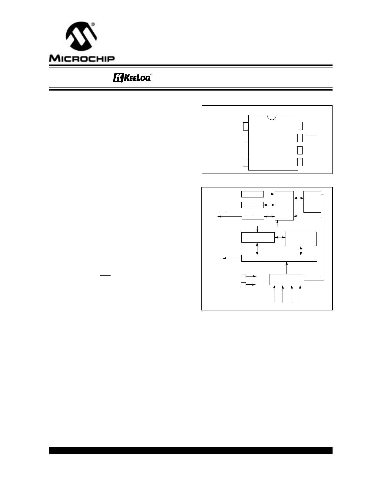
PACKA GE TYPES
PDIP, SOIC
S0
S1
S2
S3
1
2
3
4
HCS300
HCS300 BLOCK DIAGRAM
Oscillator
Controller
32-bit shift register
Button input port
LED
PWM
Reset circuit
LED driver
EEPROM
VSS
VDD
8
7
6
5
Encoder
DD
V
LED
PWM
V
SS
Power
latching
and
switching
Typical Applications
The HCS300 is ideal for Remote Keyless Entry (RKE)
applications. These applications include:
• Automotive RKE systems
• Automotive alarm systems
• Automotive immobilizers
• Gate and garage door openers
• Identity tokens
• Burglar alarm systems
DESCRIPTION
The HCS300, from Microchip Technology Inc., is a code
hopping encoder designed for secure Remote Keyless
Entry (RKE) systems. The HCS300 utilizes the K
code hopping technology , which incorporates high security, a small package outline and low cost, to make this
device a perfect solution for unidirectional remote keyless entry systems and access control systems.
KeeLoq is a trademark of Microchip Technology Inc.
*Code hopping encoder patents allowed and pending.
1996 Microchip Technology Inc.
EE
OQ
L
Preliminary
S
S
S1S
2
3
The HCS300 combines a 32-bit hopping code
generated by a non-linear encryption algorithm, with a
28-bit serial number and six status bits to create a
66-bit transmission stream. The length of the
transmission eliminates the threat of code scanning
and the code hopping mechanism makes each
transmission unique, thus rendering code capture and
resend (code grabbing) schemes useless.
The encryption key, serial number, and configuration
data are stored in EEPROM which is not accessible via
any external connection. This makes the HCS300 a
very secure unit. The HCS300 provides an easy to use
serial interface for programming the necessary security
keys, system parameters, and configuration data.
The encyrption keys and code combinations are programmable but read-protected. The keys can only be
verified after an automatic erase and programming
operation. This protects against attempts to gain
access to keys and manipulate synchronization values .
0
DS21137D-page 1
HCS300
The HCS300 operates over a wide voltage range of
2.0V to 6.3V and has four button inputs in an 8-pin
configuration. This allows the system designer the
freedom to utilize up to 15 functions. The only
components required for device operation are the buttons and RF circuitry, allowing a very low system cost.
1.0 SYSTEM OVERVIEW
ey Terms
K
ufacturer’s code - a 64-bit word, unique to
• Man
each manufacturer, used to produce a unique
encryption key in each transmitter (encoder).
• Encr
yption Key - a unique 64-bit key generated
and programmed into the encoder during the
manufacturing process. The encryption key
controls the encryption algorithm and is stored in
EEPROM on the encoder device.
1.1 Learn
The HCS product family facilitates several learn strategies to be implemented on the decoder. The following
are examples of what can be done. It must be pointed
out that their exists some third-party patents on learning strategies and implementation.
1.1.1 NORMAL LEARN
The receiver uses the same information that is transmit-
ted during normal operation to derive the transmitter’s
secret key, decrypt the discrimination value and the
synchronization counter.
1.1.2 SECURE LEARN*
The transmitter is activated through a special button
combination to transmit a stored 48-bit value (random
seed) that can be used for key generation or be part of
the key. Transmission of the random seed can be disabled after learning is completed.
The HCS300 is a code hopping encoder device that is
designed specifically for keyless entry systems,
primarily for vehicles and home garage door openers. It
is meant to be a cost-effective, yet secure solution to
such systems. The encoder portion of a keyless entry
system is meant to be held by the user and operated to
gain access to a vehicle or restricted area. The
HCS300 requires very few external components
(Figure 2-1).
Most keyless entry systems transmit the same code
from a transmitter every time a button is pushed. The
relative number of code combinations for a lo w end system is also a relatively small number. These
shortcomings provide the means for a sophisticated
thief to create a device that ‘grabs’ a transmission and
re-transmits it later or a device that scans all possible
combinations until the correct one is found.
The HCS300 employs the K
nology and an encryption algorithm to achieve a high
level of security. Code hopping is a method by which
the code transmitted from the transmitter to the receiver
is different every time a button is pushed. This method,
coupled with a transmission length of 66 bits, virtually
eliminates the use of code ‘grabbing’ or code
‘scanning’.
As indicated in the block diagram on page one, the
HCS300 has a small EEPROM array which must be
loaded with several parameters before use. The most
important of these values are:
• A 28-bit serial number which is meant to be
unique for every encoder
• An encryption key that is generated at the time of
production
• A 16-bit synchronization value
The serial number for each transmitter is programmed
by the manufacturer at the time of production. The
generation of the encryption key is done using a key
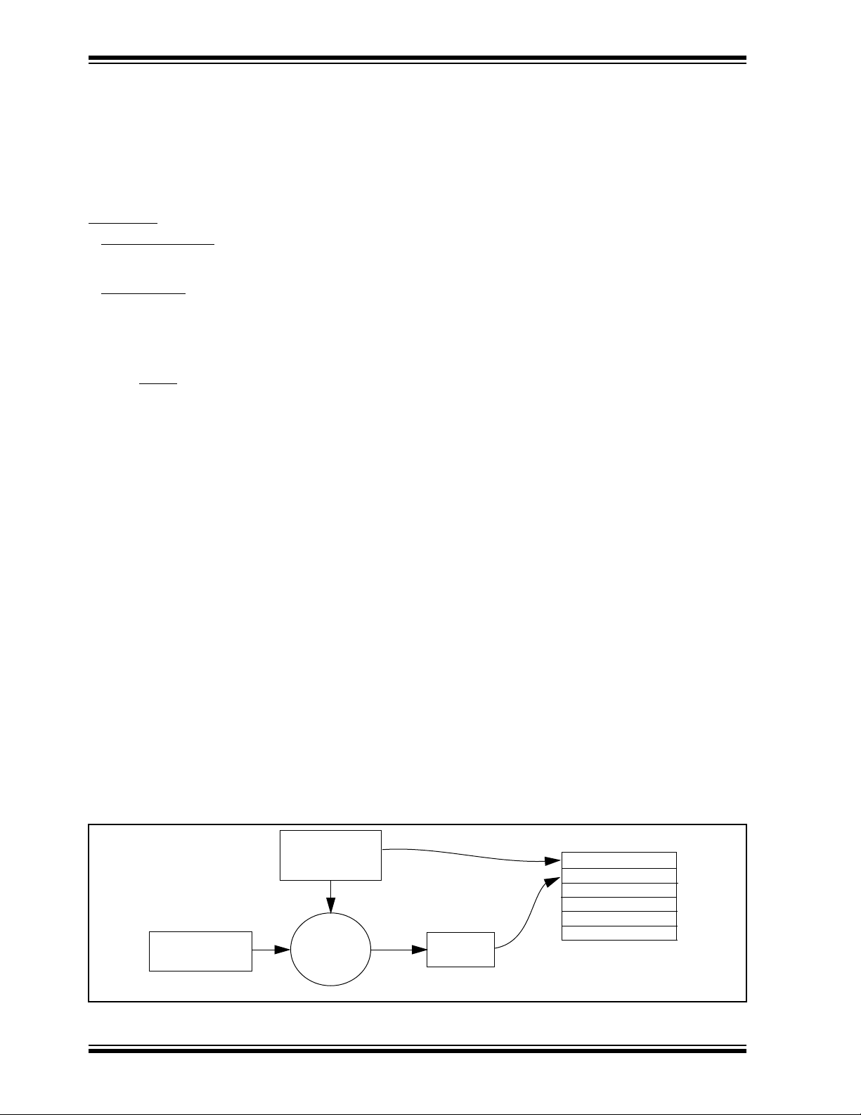
generation algorithm (Figure 1-1). Typically, inputs to
the key generation algorithm are the serial number of
the transmitter and a 64-bit manufacturer’s code. The
manufacturer’s code is chosen by the system
manufacturer and must be carefully controlled. The
manufacturer’s code is a pivotal part of the overall
system security.
EE
OQ
L
code hopping tech-
FIGURE 1-1: CREATION AND STORAGE OF ENCRYPTION KEY DURING PRODUCTION
HCS300 EEPROM Array
Serial Number
Encryption Key
Sync Counter
.
.
.
1996 Microchip Technology Inc.
Manufacturer’s
DS21137D-page 2
Code
Transmitter
Serial Number or
Seed
Key
Generation
Algorithm
Encryption
Key
Preliminary
HCS300
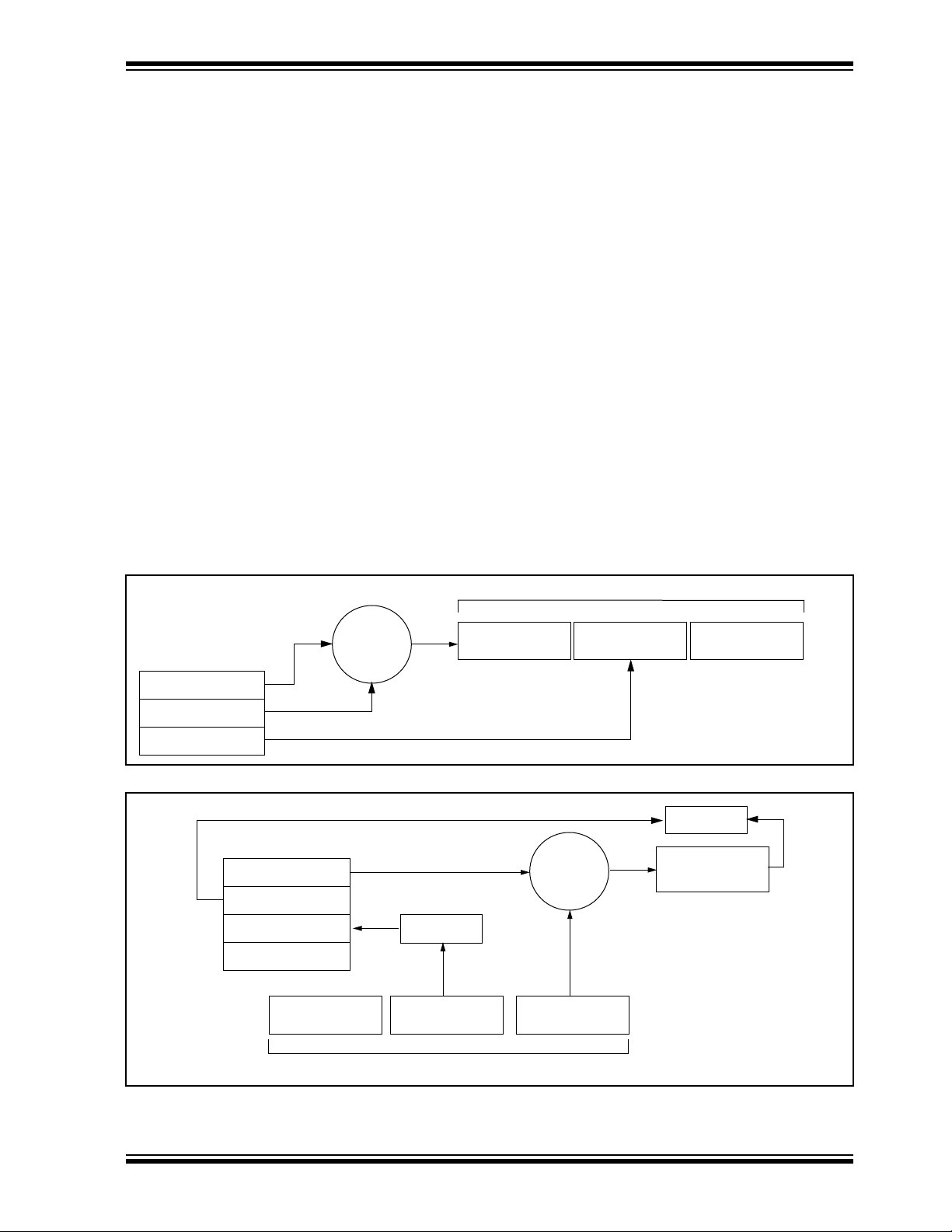
The 16-bit synchronization value is the basis for the
transmitted code changing for each transmission, and
is updated each time a button is pressed. Because of
the complexity of the code hopping encryption algorithm, a change in one bit of the synchronization value
will result in a large change in the actual transmitted
code. There is a relationship (Figure 1-2) between the
key values in EEPROM and how they are used in the
encoder. Once the encoder detects that a button has
been pressed, the encoder reads the button and
updates the synchronization counter. The synchronization value is then combined with the encryption key in
the encryption algorithm and the output is 32 bits of
encrypted information. This data will change with every
button press, hence, it is referred to as the hopping
portion of the code word. The 32-bit hopping code is
combined with the button information and the serial
number to form the code word transmitted to the
receiver. The code word format is explained in detail
in Section 4.2.
Any type of controller may be used as a receiver, but it
is typically a microcontroller with compatible firmware
that allows the receiver to operate in conjunction with a
transmitter, based on the HCS300. Section 7.0
provides more detail on integrating the HCS300 into a
total system.
Before a transmitter can be used with a particular
receiver, the transmitter must be ‘learned’ by the
receiver. Upon learning a transmitter, information is
stored by the receiver so that it may track the
transmitter, including the serial number of the
transmitter, the current synchronization value for that
transmitter and the same encryption key that is used on
the transmitter. If a receiv er receives a message of v alid
format, the serial number is checked and, if it is from a
learned transmitter, the message is decrypted and the
decrypted synchronization counter is checked against
what is stored. If the synchronization value is verified,
then the button status is checked to see what operation
is needed. Figure 1-3 shows the relationship between
some of the values stored by the receiver and the values received from the transmitter.
FIGURE 1-2: BASIC OPERATION OF TRANSMITTER (ENCODER)
Transmitted Information
EEPROM Array
Encryption Key
Sync Counter
Serial Number
KEELOQ
Encryption
Algorithm
32 Bits of
Encrypted Data
Serial Number
FIGURE 1-3: BASIC OPERATION OF RECEIVER (DECODER)
EEPROM Array
Encryption Key
Sync Counter
Serial Number
Manufacturer Code
Button Press
Information
Check for
Match
Serial Number
KEELOQ
Decryption
Algorithm
32 Bits of
Encrypted Data
Button Press
Information
Check for
Match
Decrypted
Synchronization
Counter
1996 Microchip Technology Inc.
Received Information
Preliminary
DS21137D-page 3
HCS300
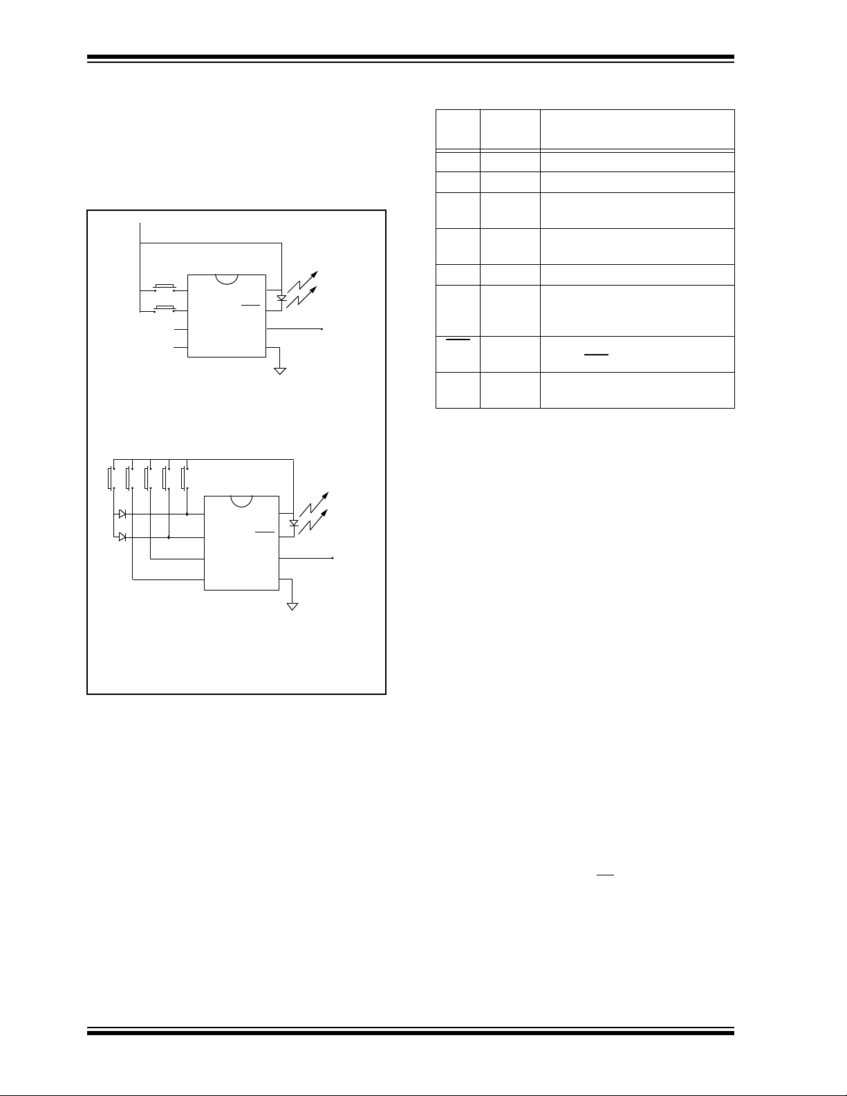
2.0 DEVICE OPERATION
As shown in the typical application circuits (Figure 2-1),
the HCS300 is a simple device to use. It requires only
the addition of buttons and RF circuitry for use as the
transmitter in your security application. A description of
each pin is described in Table 2-1.
FIGURE 2-1: TYPICAL CIRCUITS
VDD
B0
B1
B4 B3 B2 B1 B0
Note: Up to 15 functions can be implemented by
S0
S1
S2
S3
2 button remote control
5 button remote control (Note)
pressing more than one button simultaneously or by using a suitable diode array.
S0
S1
S2
S3
VDD
LED
PWM
V
SS
VDD
LED
PWM
SS
V
Tx out
VDD
Tx out
TABLE 2-1: PIN DESCRIPTIONS
Name
S0 1 Switch input 0
S1 2 Switch input 1
S2 3 Switch input 2/Can also be clock
S3 4 Switch input 3/Clock pin when in
V
SS
PWM 6 Pulse width modulation (PWM)
LED
DD
V
The high security level of the HCS300 is based on the
patented K
encryption algorithm based on a block length of 32 bits
and a key length of 64 bits is used. The algorithm
obscures the information in such a way that even if the
transmission information (before coding) diff ers b y only
one bit from the information in the previous transmission, the next coded transmission will be totally different. Statistically, if only one bit in the 32-bit string of
information changes, approximately 50 percent of the
coded transmission will change. The HCS300 will wake
up upon detecting a switch closure and then delay
approximately 10 ms for switch debounce (Figure 2-2).
The synchronized information, fixed information, and
switch information will be encrypted to form the hopping
code. The encrypted or hopping code portion of the
transmission will change every time a button is
pressed, even if the same button is pushed again.
Keeping a button pressed for a long time will result in
the same code word being transmitted until the button
is released or timeout occurs. A code that has been
transmitted will not occur again for more than 64K
transmissions. This will provide more than 18 years of
typical use before a code is repeated based on 10 operations per day. Overflow information programmed into
the encoder can be used by the decoder to extend the
number of unique transmissions to more than 192K.
If in the transmit process it is detected that a new button(s) has been pressed, a reset will immediately be
forced and the code word will not
note that buttons removed will not have any effect on
the code word unless no buttons remain pressed in
which case the ccurrent code word will be completed
and the power down will occur.
Pin
Number
Description
pin when in programming mode
programming mode
5 Ground reference connection
output pin/Data pin for
programming mode
7 Cathode connection for directly
driving LED
during transmission
8 Positive supply voltage
connection
EE
L
OQ
technology. A block cipher type of
be completed. Please
DS21137D-page 4
Preliminary
1996 Microchip Technology Inc.
HCS300
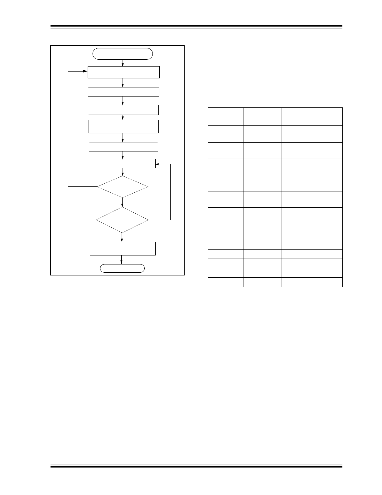
FIGURE 2-2: ENCODER OPERATION
Power Up
(A button has been pressed)
Reset and Debounce Delay
(10 ms)
Sample Inputs
Update Sync Info
Encrypt With
Encryption Key
Load T r ansmit Register
T r ansmit
Yes
Buttons
Added
?
No
All
Buttons
Released
?
Yes
Complete Code
Word Transmission
Stop
No
3.0 EEPROM MEMORY ORGANIZATION
The HCS300 contains 192 bits (12 x 16-bit words) of
EEPROM memory (Table 3-1). This EEPROM array is
used to store the encryption key information,
synchronization value, etc. Fur ther descriptions of the
memory array is given in the following sections.
TABLE 3-1: EEPROM MEMORY MAP
WORD
ADDRESS
0 KEY_0 64-bit encryption key
1 KEY_1 64-bit encryption key
2 KEY_2 64-bit encryption key
3 KEY_3 64-bit encryption key
4 SYNC 16-bit synchronization
5 RESERVED Set to 0000H
6 SER_0 Device Serial Number
7 SER_1(Note) Device Serial Number
8 SEED_0 Seed Value (word 0)
9 SEED_1 Seed Value (word 1)
10 EN_KEY 16-bit Envelope Key
11 CONFIG Config Word
Note: The MSB of the serial number contains a bit
MNEMONIC DESCRIPTION
(word 0)
(word 1)
(word 2)
(word 3)
value
(word 0)
(word 1)
used to select the auto shutoff timer.
1996 Microchip Technology Inc.
3.1 Key_0 - Key_3 (64-Bit Encryption Key)
The 64-bit encryption key is used by the transmitter to
create the encrypted message transmitted to the
receiver. This key is created and programmed at the
time of production using a key generation algorithm.
Inputs to the key generation algorithm are the serial
number for the particular transmitter being used and a
secret manufacturer’s code. While the key generation
algorithm supplied from Microchip is the typical method
used, a user may elect to create their own method of
key generation. This may be done providing that the
decoder is programmed with the same means of creating the key for decryption pur poses. If a seed is used,
the seed will also form part of the input to the key generation algorithm.
Preliminary
DS21137D-page 5

HCS300
3.2 SYNC (Synchronization Counter)
This is the 16-bit synchronization value that is used to
create the hopping code for transmission. This value
will be changed after every transmission.
3.3 SER_0, SER_1 (Encoder Serial Number)
SER_0 and SER_1 are the lower and upper words of
the device serial number, respectively. Although there
are 32 bits allocated for the serial number, only the
lower order 28 bits are transmitted. The serial number
is meant to be unique for every transmitter. The most
significant bit of the serial number (Bit 31) is used to
turn the auto shutoff timer on or off.
3.3.1 AUTO SHUTOFF TIMER SELECT
The most significant bit of the serial number (Bit 31) is
used to turn the Auto shutoff timer on or off. This timer
prevents the transmitter from draining the battery
should a button get stuck in the on position for a long
period of time. The time period is approximately
25 seconds, after which the device will go to the
Time-out mode. When in the Time-out mode, the
device will stop transmitting, although since some
circuits within the device are still active, the current
draw within the Shutoff mode will be more than
Standby mode. If the most significant bit in the serial
number is a one, then the auto shutoff timer is enabled,
and a zero in the most significant bit will disable the
timer. The length of the timer is not selectable.
3.4 SEED_0, SEED_1 (Seed Word)
This is the two word (32 bits) seed code that will be
transmitted when all four buttons are pressed at the same
time. This allows the system designer to implement the
secure learn feature or use this fixed code word as part of
a different key generation/tracking process or purely as a
fixed code transmission.
3.5 EN_Key (Envelope Encryption Key)
Envelope encryption is a selectable option that
encrypts the portion of the transmission that contains
the transmitter serial number. Selecting this option is
done by setting the appropriate bit in the configuration
word (Table 3-2). Normally, the serial number is
transmitted in the clear (un-encrypted), but for an
added level of security, the system designer may elect
to implement this option. The envelope encryption key
is used to encrypt the serial number portion of the
transmission, if the envelope encryption option has
been selected. The envelope encryption algorithm is a
different algorithm than the key generation or transmit
encryption algorithm. The EN_k e y is typically a random
number and the same for all transmitters in a system.
3.6 Configuration Wor d
The configuration word is a 16-bit word stored in
EEPROM array that is used by the device to store
information used during the encryption process, as well
as the status of option configurations. Further
explanations of each of the bits are described in the
following sections.
TABLE 3-2: CONFIGURATION WORD
Bit Number Bit Description
0 Discrimination Bit 0
1 Discrimination Bit 1
2 Discrimination Bit 2
3 Discrimination Bit 3
4 Discrimination Bit 4
5 Discrimination Bit 5
6 Discrimination Bit 6
7 Discrimination Bit 7
8 Discrimination Bit 8
9 Discrimination Bit 9
10 Overflow Bit 0 (OVR0)
11 Overflow Bit 1 (OVR1)
12 Low V oltage Trip Point Select
13 Baudrate Select Bit 0 (BSL0)
14 Baudrate Select Bit 1 (BSL1)
15 Envelope Encryption Select (EENC)
3.6.1 DISCRIMINATION VALUE (DISC0 TO DISC9)
The discrimination value can be programmed with any
value to serve as a post decryption check on the
decoder end. In a typical system, this will be
programmed with the 10 least significant bits of the
serial number, which will also be stored by the receiver
system after a transmitter has been learned. The
discrimination bits are part of the information that is to
form the encrypted portion of the transmission. After
the receiver has decrypted a transmission, the
discrimination bits can be checked against the stored
value to verify that the decryption process was valid.
3.6.2 OVERFLOW BITS (OVR0 AND OVR1)
The overflow bits are used to e xtend the number of possible synchronization values. The synchronization
counter is 16 bits in length, yielding 65,536 values
before the cycle repeats. Under typical use of
10 operations a day, this will provide nearly 18 years of
use before a repeated value will be used. Should the
system designer conclude that is not adequate, then
the overflow bits can be utilized to e xtend the number of
unique values. This can be done by programming
OVR0 and OVR1 to 1s at the time of production. The
encoder will automatically clear OVR0 the first time that
the synchronization value wraps from 0xFFFF to
0x0000 and clear OVR1 the second time the counter
wraps. Once cleared, OVR0 and OVR1 cannot be set
DS21137D-page 6
Preliminary
1996 Microchip Technology Inc.

HCS300
again, thereby creating a permanent record of the
counter overflow. This prevents fast cycling of 64K
counter. If the decoder system is programmed to track
the overflow bits, then the effective number of unique
synchronization values can be extended to 196,608. If
programmed to zero , the system will be compatible with
the NTQ104/5/6 devices (i.e., no overflow with discrimination bits set to zero).
3.6.3 ENVELOPE ENCRYPTION (EENC)
If the EENC bit is set to a 1, the 32-bit fixed code part
of the transmission will also be encrypted so that it will
appear to be random. The 16-bit envelope key and
envelope algorithm will be used for encryption.
3.6.4 BAUDRATE SELECT BITS (BSL0, BSL1)
BSL0 and BSL1 select the speed of transmission and
the code word blanking. Table 3-3 shows how the bits
are used to select the different baud rates and
Section 5.2 provides detailed explanation in code word
blanking.
TABLE 3-3: BAUDRATE SELECT
BSL1 BSL0
Basic Pulse
Element
0 0 400 µ s All
0 1 200 µ s 1 out of 2
1 0 100 µ s 1 out of 2
1 1 100 µ s 1 out of 4
3.6.5 LOW VOLTAGE TRIP POINT SELECT
The low voltage trip point select bit is used to tell the
HCS300 what V
DD
level is being used. This information
will be used by the device to determine when to send
the voltage low signal to the receiver. When this bit is
set to a one, the V
from a 5 volt or 6 volt V
the V
DD
level is assumed to be 3.0 volts. Refer to
level is assumed to be operating
DD
level. If the bit is set low, then
DD
Figure 3-1 for voltage trip point.Vlow is tested at 6.3V at
-25 ° C and +85 ° C and 2.0V at -25 ° C and +85 ° C
Code Wor ds
T ransmitted
4.0 T RANSMITTED W ORD
4.1 Transmission Format (PWM)
The HCS300 transmission is made up of several parts
(Figure 4-1). Each transmission is begun with a
preamble and a header, followed by the encrypted and
then the fixed data. The actual data is 66 bits which
consists of 32 bits of encrypted data and 34 bits of fixed
data. Each transmission is followed by a guard period
before another transmission can begin. Refer to
Table 8-4 for transmission timing requirements. The
encrypted portion provides up to four billion changing
code combinations and includes the button status bits
(based on which buttons were activated) along with the
synchronization counter value and some discrimination
bits. The fixed portion is comprised of the status bits,
the function bits and the 28-bit serial number. The fixed
and encrypted sections combined increase the number
of combinations to 7.38 x 10
4.2 Synchronous T ransmission Mode
Synchronous transmission mode can be used to clock
the code word out using an external clock.
T o enter synchronous transmission mode , the programming mode start-up sequence must be executed as
shown in Figure 4-3. If either S1 or S0 is set on the f alling edge of S2 (or S3), the device enters synchronous
transmission mode. In this mode, it functions as a normal transmitter, with the e xception that the timing of the
PWM data string is controlled externally and that 16
extra bits are transmitted at the end with he code word.
The button code will be the S0, S1 value at the falling
edge S2 or S3. The timing of the PWM data str ing is
controlled by supplying a clock on S2 or S3 and should
not exceed 20 KHz. The code word is the same as in
PWM mode with 16 reserved bits at the end of the
word. The reser ved bits can be ignored. When in synchronous transmission mode S2 or S3 should not be
toggled until all internal processing has been completed as shown in Figure 4-4.
19
.
FIGURE 3-1: TYPICAL VOLTAGE TRIP
POINTS
Volts (V)
1996 Microchip Technology Inc.
4.2
4.0
3.8
3.6
2.6
2.4
2.2
2.0
1.8
1.6
1.4
-40
05085
VLOW sel = 1
VLOW sel = 0
VLOW
Temp (C)
4.3 Code Wor d Organization
The HCS300 transmits a 66-bit code word when a button is pressed. The 66-bit word is constructed from a
Fixed Code portion and an Encrypted Code portion
(Figure 4-2).
The Encrypted Data is generated from four button bits ,
two overflow counter bits, ten discrimination bits, and
the 16-bit synchronization value (Figure 8-4).
The Fixed Code Data is made up from two status bits,
four button bits, and the 28-bit serial number. The four
button bits and the 28-bit serial number may be
encrypted with the Envelope Key if the envelope
encryption is enabled by the user.
Preliminary
DS21137D-page 7

HCS300
FIGURE 4-1: CODE WORD TRANSMISSION FORMAT
LOGIC ‘0’
LOGIC ‘1’
Bit
Period
Preamble
TP
Header
TH
Encrypted Portion
of Transmission
THOP
FIGURE 4-2: CODE WORD ORGANIZATION
Fixed Code Data
VLOW and
Repeat Status
(2 bits)
2 bits
of Status
Button
Status
(4 bits)
Serial Number and Button
+
28-bit Serial Number
Status (32 bits)
Button
Status
(4 bits)
+
FIGURE 4-3: SYNCHRONOUS TRANSMISSION MODE
t = 50 ms
PWM
Fixed Portion of
Transmission
Encrypted Code Data
Overflow
bits
(2 bits)
LOCK CIPHER
B
32 bits of Encrypted Data
TFIX
Discrimination
bits
(10 bits)
Encrypted using
Algorithm
Guard
Time
TG
16-bit
Sync Value
Transmission Direction
S2(S3)
S[1:0]
“01,10,11”
FIGURE 4-4: TRANSMISSION WORD FORMAT DURING SYNCHRONOUS TRANSMISSION MODE
Reserved Padding
Button
Code
Serial Number Data Word Sync Counter
16 2 4 28 16 16
Transmission Direction
DS21137D-page 8
Preliminary
1996 Microchip Technology Inc.

HCS300
5.0 SPECIAL FEATURES
5.1 Code Wor d Completion
Code word completion is an automatic feature that
makes sure that the entire code word is transmitted,
even if the b utton is released bef ore the transmission is
complete. The HCS300 encoder powers itself up when
a button is pushed and powers itself down after the
command is finished, if the user has already released
the button. If the button is held down beyond the time
for one transmission, then multiple transmissions will
result. If another button is activated during a
transmission, the active transmission will be aborted
and the new code will be generated using the new
button information.
5.2 Blank Alternate Code Word
Federal Communications Commission (FCC) part 15
rules specify the limits on fundamental power and
harmonics that can be transmitted. Power is calculated
on the worst case average power transmitted in a
100ms window. It is therefore advantageous to
minimize the duty cycle of the transmitted word. This
can be achieved by minimizing the duty cycle of the
individual bits and by blanking out consecutive words.
Blank Alternate Code Word (BACW) is used for
reducing the average power of a transmission
(Figure 5-1). This is a selectable feature that is
determined in conjunction with the baudrate selection
bits BSL0 and BSL1. Using the BACW allows the user
to transmit a higher amplitude transmission if the
transmission length is shorter. The FCC puts
constraints on the average power that can be
transmitted by a device , and BACW eff ectively pre v ents
continuous transmission by only allowing the transmission of every second or every fourth code word. This
reduces the average power transmitted and hence,
assists in FCC approval of a transmitter device.
5.3 Envelope Encryption Option
Envelope Encryption is a user selectable option which
is meant to offer a higher level of security for a code
hopping system. During a normal transmission with the
envelope encryption turned off, the 28-bit serial number
is transmitted in the clear (unencrypted). If envelope
encryption is selected, then the serial number is also
encrypted before transmission. The encr yption for the
serial number is done using a different algorithm than
the transmission algorithm. The envelope encryption
scheme is not nearly as complex as the KeeLoq algorithm and, hence, not as secure. When the envelope
encryption is used, the serial number must be
decrypted using the envelope key and envelope
decryption. After the serial number is obtained, the normal decryption method can be used to decrypt the hopping code. All transmitters in a system must use the
same envelope key.
5.4 Secure Learn
In order to increase the level of security in a system, it is
possible for the receiver to implement what is known as
a secure learn function. This can be done b y utilizing the
seed value on the HCS300 which is stored in EEPROM
and can only be transmitted when all four button inputs
are pressed at the same time (Table 5-1). Instead of the
normal key generation method being used to create the
encryption key, this seed value is used and there need
not be any mathematical relationship between serial
numbers and seeds.
TABLE 5-1: PIN ACTIVATION TABLE
S3 S2 S1 S0 Notes
100011
200101
300111
401001
501011
601101
701111
810001
910011
10 1 0 1 0 1
11 1 0 1 1 1
12 1 1 0 0 1
13 1 1 0 1 1
14 1 1 1 0 1
15 1 1 1 1 2
Note 1: Transmit generated 32-bit code hopping
word.
2: Transmit 32-bit seed value.
5.5 Auto-shutoff
The Auto-shutoff function automatically stops the
device from transmitting if a button inadvertently gets
pressed for a long period of time. This will prevent the
device from draining the battery if a button gets pressed
while the transmitter is in a pocket or purse. This function can be enabled or disabled and is selected by setting or clearing the Auto-shutoff bit (see Section 3.3.1).
Setting this bit high will enable the function (turn
Auto-shutoff function on) and setting the bit low will disable the function. Time-out period is approximately 25
seconds.
1996 Microchip Technology Inc.
Preliminary DS21137D-page 9

HCS300
FIGURE 5-1: BLANK ALTERNATE CODE WORD (BACW)
Amplitude
One Code Word
100ms
BACW Disabled
(All words transmitted)
BACW Enabled
(1 out of 2 transmitted)
BACW Enabled
(1 out of 4 transmitted)
A
2A
4A
5.6 VLOW: Voltage LOW Indicator
The VLOW bit is transmitted with every transmission
(Figure 8-4) and will be transmitted as a one if the
operating voltage has dropped below the low voltage
trip point. The trip point is selectable between two
values, based on the battery voltage being used. See
Section 3.6.5 for a description of how the low voltage
select option is set. This VLOW signal is transmitted so
the receiver can give an audible signal to the user that
the transmitter battery is low (Section 5.8).
100ms
Time
100ms
100ms
5.7 RPT: Repeat Indicator
This bit will be low for the first transmitted word. If a
button is held down for more than one tr ansmitted code
word, this bit will be set to indicate a repeated code
word and remain set until the button is released
(Figure 8-4).
5.8 LED Output Operation
During normal transmission the LED output is LOW. If
the supply voltage drops below the low voltage trip
point, the LED
5Hz during the transmission (Section 3.6.5).
output will be toggled at approximately
DS21137D-page 10 Preliminary 1996 Microchip Technology Inc.

HCS300
6.0 PROGRAMMING THE HCS300
When using the HCS300 in a system, the user will have
to program some parameters into the device including
the serial number and the secret key before it can be
used. The programming cycle allows the user to input
all 192 bits in a serial data stream, which are then
stored internally in EEPROM. Programming will be
initiated by forcing the PWM line high, after the S3 line
has been held high for the appropriate length of time
line (Table 6-1 and Figure 6-1). After the program mode
is entered, a delay must be provided to the device for
the automatic bulk write cycle to complete. This will
write all locations in the EEPROM to an all zeros pattern. The device can then be programmed by clocking
in 16 bits at a time, using S3 as the clock line and PWM
as the data in line. After each 16-bit word is loaded, a
programming delay is required for the internal program
FIGURE 6-1: PROGRAMMING WAVEFORMS
S3
(Clock)
PWM
(Data)
Enter Program
Mode
TPS
TPH1
T
PBW
TCLKH
TCLKL
Bit 0 Bit 1 Bit 2 Bit 3 Bit 14 Bit 15 Bit 16 Bit 17
TDS
cycle to complete. This delay can take up to Twc. At the
end of the programming cycle, the device can be verified (Figure 6-2) by reading back the EEPROM. Reading is done by clocking the S3 line and reading the data
bits on PWM. For security reasons, it is not possible to
execute a verify function without first programming the
EEPROM. A verify operation can only be done
once, immediately following the program cycle.
Note: To ensure that the device does not acci-
dentally enter programming mode, PWM
should never be pulled high by the circuit
connected to it. Special care should be
taken when driving PNP RF transistors.
TWC
TDH
TPH2
Note 1: Unused button inputs to be held to ground during the entire programming sequence.
Note 2: The VDD pin must be taken to ground after a program/verify cycle.
Data for Word 0 (KEY_0)
Repeat 12 times for each word
FIGURE 6-2: VERIFY WAVEFORMS
End of
Programming Cycle
PWM
(Data)
S3
(Clock)
Note: If a Verify operation is to be done, then it must immediately follow the Program cycle.
Begin Verify Cycle Here
Bit 0Bit191Bit190
TWC
Data in Word 0
Bit 1 Bit 2 Bit 3 Bit 15Bit 14 Bit 16 Bit 17 Bit190 Bit191
TDV
Data for Word 1
1996 Microchip Technology Inc. Preliminary DS21137D-page 11

HCS300
TABLE 6-1: PROGRAMMING/VERIFY TIMING REQUIREMENTS
VDD = 5.0V ± 10%
25° C ± 5 °C
Parameter Symbol Min. Max. Units
Program mode setup time T
Hold time 1 T
Hold time 2 T
Bulk Write time T
Program delay time T
Program cycle time T
Clock low time T
Clock high time T
Data setup time T
Data hold time T
Data out valid time T
PS 3.5 4.5 ms
PH1 3.5 — ms
PH250 — µs
PBW — 2.2 ms
PROG — 2.2 ms
WC —36ms
CLKL 25 — µs
CLKH 25 — µs
DS 0—µs
DH 18 — µs
DV 10 24 µs
DS21137D-page 12 Preliminary 1996 Microchip Technology Inc.

HCS300
7.0 INTEGRATING THE HCS300 INTO A SYSTEM
Use of the HCS300 in a system requires a compatible
decoder. This decoder is typically a microcontroller with
compatible firmware. Microchip will provide (via a
license agreement) firmware routines that accept
transmissions from the HCS300 and decrypt the
hopping code portion of the data stream. These
routines provide system designers the means to
develop their own decoding system.
7.1 Learning a Transmitter to a Receiver
In order for a transmitter to be used with a decoder , the
transmitter must first be ‘learned’. Several learning
strategies can be followed in the decoder implementation. When a transmitter is lear ned to a decoder, it is
suggested that the decoder stores the serial number
and current synchronization value in EEPROM. The
decoder must keep track of these values for every
transmitter that is learned (Figure 7-1). The maximum
number of transmitters that can be learned is only a
function of how much EEPROM memory storage is
available. The decoder must also store the manufacturer’s code in order to learn a transmission transmitter ,
although this value will not change in a typical system
so it is usually stored as part of the microcontroller
ROM code. Storing the manufacturer’s code as part of
the ROM code is also better for security reasons.
It must be stated that some learning strategies have
been patented and care must be taken not to infringe.
FIGURE 7-1: TYPICAL LEARN SEQUENCE
Enter Learn
Mode
Wait for Reception
of a Valid Code
Generate Key
from Serial Number
Use Generated Key
to Decrypt
Compare Discrimination
Value with Fixed Value
Equal
?
Yes
Wait for Reception
of Second Valid Code
Use Generated Key
to Decrypt
Compare Discrimination
Value with Fixed Value
Equal
?
Yes
No
No
Counters
Sequential
?
Yes
Learn successful Store:
Serial number
Encryption key
Synchronization counter
Exit
No
Learn
Unsuccessful
1996 Microchip Technology Inc. Preliminary DS21137D-page 13

HCS300
7.2 Decoder Operation
In a typical decoder operation (Figure 7-2), the key generation on the decoder side is done by taking the serial
number from a transmission and combining that with
the manufacturer’s code to create the same secret key
that was used by the transmitter . Once the secret key is
obtained, the rest of the transmission can be decrypted.
The decoder waits for a transmission and immediately
can check the serial number to determine if it is a
learned transmitter. If it is, it tak es the encrypted portion
of the transmission and decrypts it using the stored key
It uses the discrimination bits to determine if the
decryption was valid. If everything up to this point is
valid, the synchronization value is evaluated.
FIGURE 7-2: TYPICAL DECODER
OPERATION
Start
No
Transmission
Received
?
Yes
No
Decrypt T ransmission
Does
Serial Number
Match
?
Yes
7.3 Synchronization with Decoder
The KEELOQ technology features a sophisticated
synchronization technique (Figure 7-3) which does not
require the calculation and storage of future codes. If
the stored counter value for that particular transmitter
and the counter value that was just decrypted are within
a formatted window of say 16, the counter is stored and
the command is executed. If the counter value was not
within the single operation window, but is within the
double operation window of sa y 32K window , the tr ansmitted synchronization value is stored in temporary
location and it goes back to waiting for another transmission. When the next valid transmission is received,
it will check the new value with the one in temporary
storage. If the two values are sequential, it is assumed
that the counter had just gotten out of the single operation ‘window’, but is now back in sync, so the new synchronization value is stored and the command
executed. If a transmitter has somehow gotten out of
the double operation window, the transmitter will not
work and must be re-learned. Since the entire window
rotates after each valid transmission, codes that have
been used are part of the ‘block ed’ (32K) codes and are
no longer valid. This eliminates the possibility of grabbing a previous code and re-transmitting to gain entry.
Note: The synchronization method described in
this section is only a typical implementation
and because it is usually implemented in
firmware, it can be altered to fit the needs
of a particular system
FIGURE 7-3: SYNCHRONIZATION WINDOW
No
Decryption
Valid
No
No
Counter
Within 16
Counter
Within 32K
Save Counter
in T emp Location
Is
?
Yes
Is
?
No
Is
?
Yes
Yes
Execute
Command
and
Update
Counter
Entire Window
rotates to eliminate
use of previously
used codes
Double
Operation
(32K Codes)
Blocked
(32K Codes)
Current
Position
Single Operation
Window (16 Codes)
DS21137D-page 14 Preliminary 1996 Microchip Technology Inc.

HCS300
8.0 ELECTRICAL CHARACTERISTICS
TABLE 8-1: ABSOLUTE MAXIMUM RATINGS
Symbol Item Rating Units
DD Supply voltage -0.3 to 6.6 V
V
IN Input voltage -0.3 to VDD + 0.3 V
V
OUT Output voltage -0.3 to VDD + 0.3 V
V
OUT Max output current 50 mA
I
STG Storage temperature -55 to +125 C (Note)
T
LSOL Lead soldering temp 300 C (Note)
T
ESD ESD rating 4000 V
V
Note: Stresses above those listed under “ABSOLUTE MAXIMUM RATINGS” may cause permanent damage to
the device.
TABLE 8-2: DC CHARACTERISTICS
Commercial (C): Tamb = 0°C to +70°C
Industrial (I): Tamb = -40°C to +85°C
2.0V < V
Parameter Sym. Min Typ
Operating current (avg)
2
Standby current I
Auto-shutoff
3,4
current
High level Input
ICC 0.2 0.5
CCS 0.1 1.0 0.1 1.0 µA
ICCS 40 75 160 650 µA
IH 0.55VDD VDD+0.3 0.55VDD VDD+0.3 V
V
voltage
Low level input
IL -0.3 0.15VDD -0.3 0.15VDD V
V
voltage
High level output
OH 0.7VDD
V
voltage
Low level output
OL 0.08VDD
V
voltage
sink
LED
5
current
Resistance;
ILED 1.0 1.8 2.5
SO-3 40 60 80 40 60 80 kΩ VDD = 4.0V
R
S0-S3
Resistance;
PWM 80 120 160 80 120 160 kΩ VDD = 4.0V
R
PWM
Note 1: Typical values are at 25°C.
2: No load.
3: Auto-shutoff current specification does not include the current through the input pulldown resistors.
4: Auto-shutoff current is periodically sampled and not 100% tested.
5: With VLOW Sel = 0 for operation from 2.0V to 3.0V and VLOW Sel = 1 for operation from 3.0V to 6.3V.
6: V
LED is the voltage drop across the terminals of the LED.
DD < 3.0 3.0 < VDD < 6.3
1
Max Min Typ
1
0.7 1.4mAmA
0.7VDD
0.08V
2.0 2.7 3.7mAmA
Max Unit Conditions
VDD = 3.0V
V
DD = 6.3V
VVIOH = -1.0 mA VDD = 2.0V
I
OH = -2.0 mA VDD = 6.3V
VVIOL = 1.0 mA VDD = 2.0V
DD
I
OL = 2.0 mA VDD = 6.3V
VLED6 = 1.5V VDD = 3.0V
6
V
LED
= 1.5V VDD = 6.3V
1996 Microchip Technology Inc. Preliminary DS21137D-page 15

HCS300
FIGURE 8-1: POWER UP AND TRANSMIT TIMING
Button Press
PWM
Sn
Detect
DB
T
TTD
T
BP
Code
Word
1
TABLE 8-3: POWER UP AND TRANSMIT TIMING REQUIREMENTS
VDD = +2.0 to 6.3V
Commercial (C): Tamb = 0°C to +70°C
Industrial (I): Tamb = -40°C to +85°C
Code Word Transmission
Code
Word
2
TTO
Code
Word
3
Code
Word
n
Parameter Symbol Min Max Unit Remarks
Time to second button press T
Transmit delay from button detect T
Debounce delay T
Auto-shutoff time-out period T
Note 1: TBP is the time in which a second button can be pressed without completion of the first code word and the
intention was to press the combination of buttons.
2: The auto shutoff timeout period is not tested.
BP 10 + Code
Word Time
TD 10 26 ms
DB 613ms
TO 20 35 s
26 + Code
Word Time
ms
(Note 1)
(Note 2)
FIGURE 8-2: PWM FORMAT
TE
TE
TE
LOGIC ‘0’
LOGIC ‘1’
TBP
Preamble
TP
Header
TH
Encrypted Portion
of Transmission
THOP
Fixed portion of
Transmission
TFIX
Guard
Time
TG
FIGURE 8-3: PREAMBLE/HEADER FORMAT
Data Word
P1
DS21137D-page 16 Preliminary 1996 Microchip Technology Inc.
Preamble Header
P12
23 TE
10 TE
Transmission
Bit 0 Bit 1

FIGURE 8-4: DATA WORD FORMAT
LSB
LSB
MSB MSB S3 S0 S1 S2 VLOW RPT
HCS300
Serial Number Button Code Status
Header
Bit 0 Bit 1
Hopping Code Word
Bit 30
Bit 31 Bit 32 Bit 33 Bit 58 Bit 59
Bit 60
Bit 61
Fixed Code Word
Bit 62 Bit 63 Bit 64 Bit 65
TABLE 8-4: CODE WORD TRANSMISSION TIMING REQUIREMENTS
VDD = +2.0 to 6.0V
Commercial (C): Tamb = 0°C to +70°C
Industrial (I): Tamb = -40°C to +85°C
Symbol Characteristic
Number
of T
Min. Typ. Max. Min. T yp. Max. Min. Typ. Max. Units
E
All 1 out of 2 1 out of 4
TE Basic pulse element 1 260 400 660 130 200 330 65 100 165 µs
BP PWM bit pulse width 3 780 1200 1980 390 600 990 195 300 495 µs
T
P Preamble duration 23 6.0 9.2 15.2 3.0 4.6 7.6 1.5 2.3 3.8 ms
T
H Header duration 10 2.6 4.0 6.6 1.3 2.0 3.3 0.7 1.0 1.7 ms
T
HOP Hopping code duration 96 25.0 38.4 63.4 12.5 19.2 31.7 6.2 9.6 15.8 ms
T
FIX Fixed code duration 102 26.5 40.8 67.3 13.3 20.4 33.7 6.6 10.2 16.8 ms
T
G Guard Time 39 10.1 15.6 25.7 5.1 7.8 12.9 2.5 3.9 6.4 ms
T
T otal Transmit Time 270 70.2 108.0 178.2 35.1 54.0 89.1 17.6 27.0 44.6 ms
PWM data rate 1282 833 505 2564 1667 1010 5128 3333 2020 bps
Note: The timing parameters are not tested but derived from the oscillator clock.
Code Wor ds T ransmitted
Guard
Time
FIGURE 8-5: HCS300 TE VS. TEMP
1.7
1.6
1.5
1.4
1.3
1.2
1.1
1.0
0.9
0.8
0.7
0.6
-50 -40 -30 -20 -10 0 10 20 30 40 50 60 70 80 90
TE Max.
TE Min.
Typical
LEGEND
= 2.0
= 3.0
= 6.0
1996 Microchip Technology Inc. Preliminary DS21137D-page 17

HCS300
NOTES:
DS21137D-page 18 Preliminary 1996 Microchip Technology Inc.

HCS300
HCS300 Product Identification System
To order or to obtain information (e.g., on pricing or delivery), please use the listed part numbers, and refer to the factory or the listed
sales offices.
HCS300 - /P
Package:
P = Plastic DIP (300 mil Body), 8-lead
SN = Plasitic SOIC (150 mil body), 8-lead
Temperature
Range:
Device:
Blank = 0˚C to +70˚C
I = –40˚C to +85˚C
HCS300
HCS300T
Code Hopping Encoder
Code Hopping Encoder (Tape and Reel)
Sales and Support
Products supported by a preliminary Data Sheet may possibly have an errata sheet describing minor operational differences and
recommended workarounds. To determine if an errata sheet exists for a particular device, please contact one of the following:
Your local Microchip sales office (see next page)
1.
The Microchip Corporate Literature Center U.S. FAX: (602) 786-7277
2.
The Microchip’s Bulletin Board, via your local CompuServe number (CompuServe membership NOT required).
3.
Please specify which device, revision of silicon and Data Sheet (include Literature #) you are using.
For latest version information and upgrade kits for Microchip Development Tools, please call 1-800-755-2345 or 1-602-786-7302.
1996 Microchip Technology Inc. Preliminary DS21137D-page 19

WORLDWIDE SALES & SERVICE
AMERICAS
Corporate Office
Microchip T echnology Inc.
2355 West Chandler Blvd.
Chandler, AZ 85224-6199
Tel: 602 786-7200 Fax: 602 786-7277
Technical Support:
Web:
http://www.microchip.com
Atlanta
Microchip T echnology Inc.
500 Sugar Mill Road, Suite 200B
Atlanta, GA 30350
Tel: 770 640-0034 Fax: 770 640-0307
Boston
Microchip T echnology Inc.
5 Mount Royal Avenue
Marlborough, MA 01752
Tel: 508 480-9990 Fax: 508 480-8575
Chicago
Microchip T echnology Inc.
333 Pierce Road, Suite 180
Itasca, IL 60143
Tel: 708 285-0071 Fax: 708 285-0075
Dallas
Microchip T echnology Inc.
14651 Dallas Parkway, Suite 816
Dallas, TX 75240-8809
Tel: 972 991-7177 Fax: 972 991-8588
Dayton
Microchip T echnology Inc.
Suite 150
Two Prestige Place
Miamisburg, OH 45342
Tel: 513 291-1654 Fax: 513 291-9175
Los Angeles
Microchip T echnology Inc.
18201 Von Karman, Suite 1090
Irvine, CA 92612
Tel: 714 263-1888 Fax: 714 263-1338
New Y ork
Microchip T echnology Inc.
150 Motor Parkway, Suite 416
Hauppauge, NY 11788
Tel: 516 273-5305 Fax: 516 273-5335
San Jose
Microchip T echnology Inc.
2107 North First Street, Suite 590
San Jose, CA 95131
Tel: 408 436-7950 Fax: 408 436-7955
Toronto
Microchip T echnology Inc.
5925 Airport Road, Suite 200
Mississauga, Ontario L4V 1W1, Canada
Tel: 905 405-6279 Fax: 905 405-6253
602 786-7627
ASIA/PACIFIC
Hong Kong
Microchip T echnology
RM 3801B, Tower Two
Metroplaza
223 Hing Fong Road
Kwai Fong, N.T. Hong Kong
Tel: 852 2 401 1200 Fax: 852 2 401 3431
India
Microchip T echnology
No. 6, Legacy, Convent Road
Bangalore 560 025 India
Tel: 91 80 526 3148 Fax: 91 80 559 9840
Korea
Microchip T echnology
168-1, Youngbo Bldg. 3 Floor
Samsung-Dong, Kangnam-Ku,
Seoul, Korea
Tel: 82 2 554 7200 Fax: 82 2 558 5934
Shanghai
Microchip T echnology
Unit 406 of Shanghai Golden Bridge Bldg.
2077 Yan’an Road West, Hongiao District
Shanghai, Peoples Republic of China
Tel: 86 21 6275 5700
Fax: 011 86 21 6275 5060
Singapore
Microchip T echnology
200 Middle Road
#10-03 Prime Centre
Singapore 188980
Tel: 65 334 8870 Fax: 65 334 8850
Taiwan, R.O.C
Microchip T echnology
10F-1C 207
Tung Hua North Road
T aipei, Taiwan, ROC
Tel: 886 2 717 7175 Fax: 886 2 545 0139
EUROPE
United Kingdom
Arizona Microchip Technology Ltd.
Unit 6, The Courtyard
Meadow Bank, Furlong Road
Bourne End, Buckinghamshire SL8 5AJ
Tel: 44 1628 850303 Fax: 44 1628 850178
France
Arizona Microchip Technology SARL
Zone Industrielle de la Bonde
2 Rue du Buisson aux Fraises
91300 Massy - France
Tel: 33 1 69 53 63 20 Fax: 33 1 69 30 90 79
Germany
Arizona Microchip Technology GmbH
Gustav-Heinemann-Ring 125
D-81739 Muenchen, Germany
Tel: 49 89 627 144 0 Fax: 49 89 627 144 44
Italy
Arizona Microchip Technology SRL
Centro Direzionale Colleone Pas Taurus 1
Viale Colleoni 1
20041 Agrate Brianza
Milan Italy
Tel: 39 39 6899939 Fax: 39 39 689 9883
JAPAN
Microchip Technology Intl. Inc.
Benex S-1 6F
3-18-20, Shin Yokohama
Kohoku-Ku, Yokohama
Kanagawa 222 Japan
Tel: 81 45 471 6166 Fax: 81 45 471 6122
11/7/96
All rights reserved. 1996, Microchip Technology Incorporated, USA. 11/96
Printed on recycled paper.
Information contained in this publication regarding device applications and the like is intended through suggestion only and may be superseded by updates. No representation or warranty is given and no liability is assumed by Microchip Technology Incorporated with respect to the accuracy or use of such information, or infringement
of patents or other intellectual property rights arising from such use or otherwise. Use of Microchip’s products as critical components in life support systems is not authorized except with express written approval by Microchip. No licenses are conv e y ed, implicitly or otherwise, under an y intellectual property rights. The Microchip logo and
name are registered trademarks of Microchip Technology Inc. All rights reserved. All other trademarks mentioned herein are the property of their respective companies.
DS21137D-page 20 Preliminary 1996 Microchip Technology Inc.
 Loading...