

Microchip Technology Inc 93LC76-SN, 93LC76-P, 93LC86T-I-SN, 93LC86T-I-P, 93LC86T-SN Datasheet
...
93LC76/86
8K/16K 2.5V Microwire
FEATURES
• Single supply with programming operation down
to 2.5V
• Low power CMOS technology
- 1 mA active current typical
-5 µ A standby current (typical) at 3.0V
• ORG pin selectable memory configuration
1024 x 8 or 512 x 16 bit organization (93LC76)
2048 x 8 or 1024 x 16 bit organization (93LC86)
• Self-timed ERASE and WRITE cycles
(including auto-erase)
• Automatic ERAL before WRAL
• Power on/off data protection circuitry
• Industry standard 3-wire serial I/O
• Device status signal during ERASE/WRITE cycles
• Sequential READ function
• 10,000,000 ERASE/WRITE cycles guaranteed
• Data retention > 200 years
• 8-pin PDIP/SOIC package
• Temperature ranges available
- Commercial (C) 0 ° C to +70 ° C
- Industrial (I) -40 ° C to +85 ° C
Serial EEPROM
P ACKA GE TYPES
DIP Package
93LC76/86
1
CS
2
CLK
3
DI
4
DO
SOIC Package
93LC76/86
DI
1
2
3
4
CS
CLK
DO
BLOCK DIAGRAM
VCCV
SS
8
V
CC
7
PE
6
ORG
5
V
SS
8
V
CC
7
PE
6
ORG
V
5
SS
DESCRIPTION
The Microchip Technology Inc. 93LC76/86 are 8K and
16K low voltage serial Electrically Erasable PROMs.
The device memory is configured as x8 or x16 bits
depending on the ORG pin setup. Advanced CMOS
technology makes these devices ideal for low power
non-volatile memory applications. These devices also
have a Program Enable (PE) pin to allow the user to
write protect the entire contents of the memory array.
The 93LC76/86 is available in standard 8-pin DIP and
8-pin surface mount SOIC packages.
Microwire is a registered trademark of National Semiconductor Incorporated.
PE
CS
CLK
Memory
Array
Data
Register
DI
Mode
Decode
Logic
Clock
Generator
Address
Decoder
Address
Counter
Output
Buffer
DO
1996 Microchip Technology Inc.
Preliminary
DS21131C-page 1
93LC76/86
≤
≥
≥
µ
µ
µ A µ
µ
1.0 ELECTRICAL CHARACTERISTICS
1.1 Maxim
CC
V
...................................................................................7.0V
All inputs and outputs w.r.t. V
Storage temperature.....................................-65˚C to +150˚C
Ambient temp. with power applied................. -65˚C to +125˚C
Soldering temperature of leads (10 seconds).............+300˚C
ESD protection on all pins................................................4 kV
*Notice: Stresses above those listed under “Maximum ratings”
may cause permanent damage to the device. This is a stress rating only and functional operation of the device at those or any
other conditions above those indicated in the operational listings
of this specification is not implied. Exposure to maximum rating
conditions for extended periods may affect device reliability
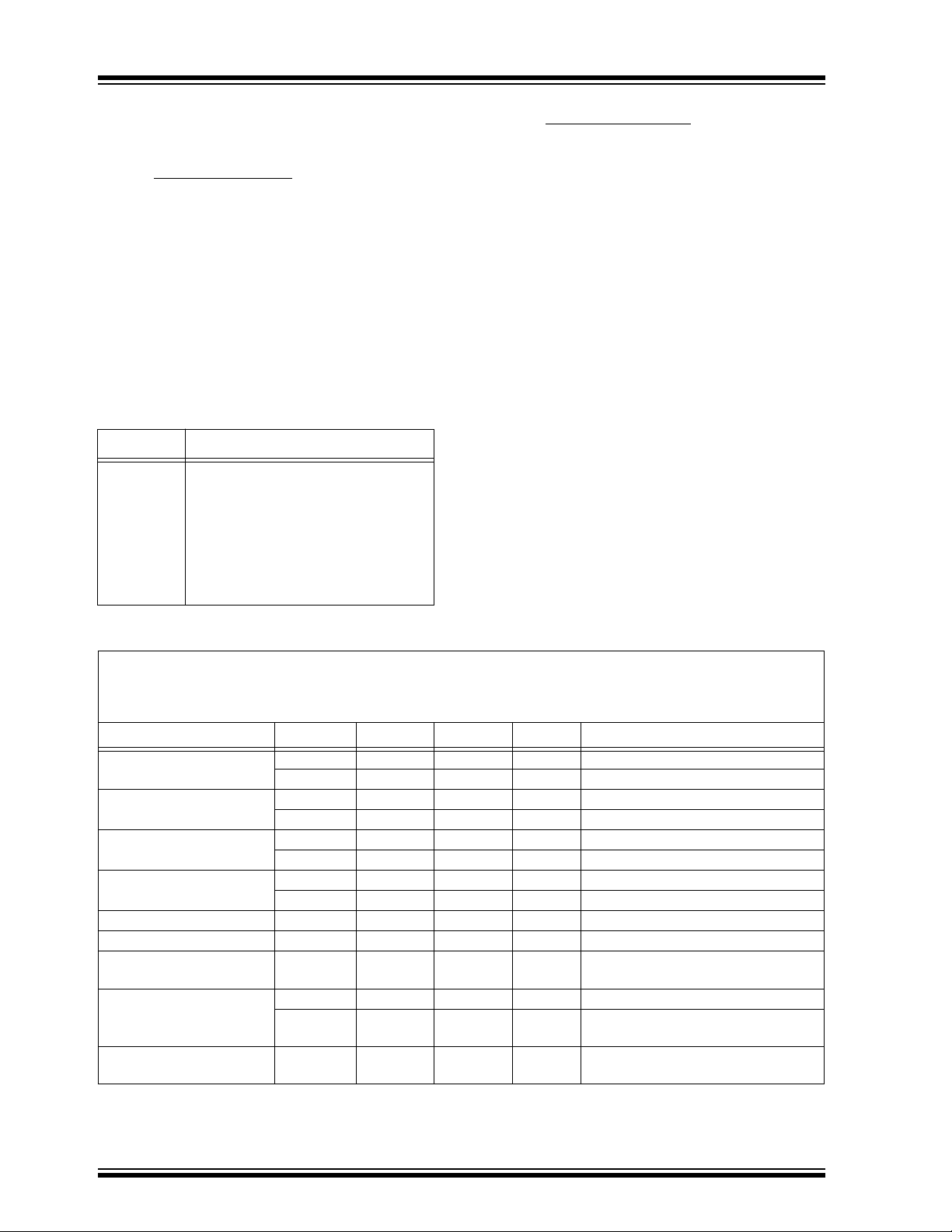
TABLE 1-1: PIN FUNCTION TABLE
Name Function
CS
CLK
DI
DO
V
SS
ORG
PE
V
CC
um Ratings*
SS
............... -0.6V to Vcc +1.0V
Chip Select
Serial Data Clock
Serial Data Input
Serial Data Output
Ground
Memory Configuration
Program Enable
Power Supply
1.2 A
C Test Conditions
AC Waveform:
= 2.0V
LO
V
HI
V
= Vcc - 0.2V
HI
V
= 4.0V for
(Note 1)
(Note 2)
Timing Measurement Reference Level
Input 0.5 V
Output 0.5 V
Note 1: For V
2: For V
CC
CC
4.0V
> 4.0V
CC
CC
TABLE 1-2: DC CHARACTERISTICS
Applicable over recommended operating ranges shown below unless otherwise noted:
V
= +2.5V to +6.0V
CC
Commercial (C): Tamb = 0˚C to +70˚C
Industrial (I): Tamb = -40˚C to +85˚C
Parameter Symbol Min. Max. Units Conditions
High level input voltage V
Low level input voltage V
Low level output voltage V
High level output voltage V
Input leakage current I
Output leakage current I
Pin capacitance
(all inputs/outputs)
Operating current I
Standby current I
Note: This parameter is periodically sampled and not 100% tested.
IH1
V
IH2
IL1
V
IL2
OL1
V
OL2
OH1
OH2
V
LI
LO
C
INT
CC
write — 3 mA V
I
read — 1
CC
2.0 V
0.7 V
CC
-0.3 0.8 V V
-0.3 0.2 V
— 0.4 V I
— 0.2 V I
2.4 — V I
CC
V
-0.2 — V I
-10 10
-10 10
—7pF
CC
+1 V V
V
CC
+1 V V
VV
CC
mA
500
CCS
— 100
30
CC
CC
< 2.7V
CC
< 2.7V
CC
OL
= 2.1 mA; V
=100 µ A; V
OL
OH
= -400 µ A; V
OH
= -100 µ A; V
AV
AV
= 0.1V to V
IN
OUT
(Note Note:)
Tamb = +25˚C, F
CC
= 5.5V
F
CLK
A
F
CLK
CLK = CS = 0V; V
A
CLK = CS = 0V; V
2.7V
2.7V
= 0.1V to V
= 3 MHz; V
= 1 MHz; V
CC
CC
CC
CC
CC
CC
CC
= 4.5V
= V
CC
= 4.5V
= V
CC
CLK
= 1 MHz
= 5.5V
= 3.0V
= 5.5V
CC
CC
= 3.0V
Min.
CC
Min.
DS21131C-page 2
Preliminary
1996 Microchip Technology Inc.
93LC76/86
TABLE 1-3: AC CHARACTERISTICS
Applicable over recommended operating ranges shown below unless otherwise noted:
V
CC
= +2.5V to +6.0V
Commercial (C): Tamb = 0˚C to +70˚C
Industrial (I): Tamb = -40˚C to +85˚C
Parameter Symbol Min. Max. Units Conditions
Clock frequency F
Clock high time T
Clock low time T
Chip select setup time T
Chip select hold time T
Chip select low time T
Data input setup time T
Data input hold time T
Data output delay time T
Data output disable time T
Status valid time T
Program cycle time T
CLK
CKH
CKL
CSS
CSH 0—ns
CSL 250 — ns Relative to CLK
DIS 50
DIH 50
PD — 100
CZ — 100
SV — 200
WC — 5 ms ERASE/WRITE mode
T
EC — 15 ms ERAL mode
T
WL — 30 ms WRAL mode
Endurance — 10M — cycles 25°C, Vcc = 5.0V, Block Mode
Note 1: This parameter is periodically sampled and not 100% tested.
2: This parameter is not tested but guaranteed b y characterization. For endurance estimates in a specific appli-
cation, please consult the Total Endurance Model which can be found on our BBS or website.
—3
2
200
—nsns4.5V ≤ V
300
100
—nsns4.5V ≥ V
200
50
—nsns4.5V ≤
100
—nsns4.5V ≤ VCC ≤ 6.0V, Relative to CLK
100
—nsns4.5V ≤ VCC ≤ 6.0V, Relative to CLK
100
250
500
300
MHz
MHz
ns
ns
ns
ns
ns
ns
4.5V ≤ V
2.5V ≤ V
2.5V ≤ V
2.5V ≤ V
CC
CC
CC
CC
CC
CC
6.0V
4.5V
6.0V
4.5V
6.0V
4.5V
VCC ≤ 6.0V, Relative to CLK
2.5V ≤ V
2.5V ≤ V
2.5V ≤ V
CC < 4.5V, Relative to CLK
CC <4.5V, Relative to CLK
CC < 4.5V, Relative to CLK
4.5V ≤ VCC ≤ 6.0V, CL = 100 pF
2.5V ≤ V
CC < 4.5V, CL = 100 pF
4.5V ≤ VCC ≤ 6.0V
2.5V ≤ V
CC < 4.5V (Note 1)
4.5V ≥ VCC ≤ 6.0V, CL = 100 pF
2.5V ≤ V
CC <4.5V, CL = 100 pF
(Note 2)
≤
<
≤
<
≤
<
1996 Microchip Technology Inc.
Preliminary
DS21131C-page 3
93LC76/86
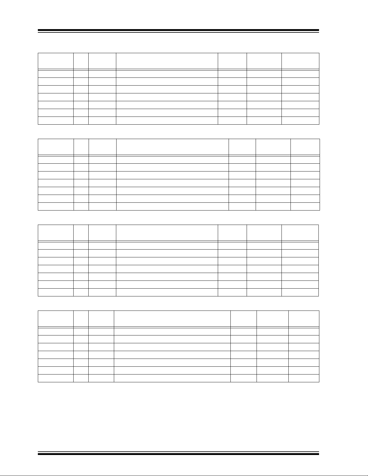
TABLE 1-4: INSTRUCTION SET FOR 93LC76: ORG=1 (1X16 ORGANIZATION)
Instruction SB Opcode Address Data In Data Out
READ 1 10 X A8 A7 A6 A5 A4 A3 A2 A1 A0 — D15 - D0 29
EWEN 1 00 1 1 XXXXXXXX — High-Z 13
ERASE 1 11 X A8 A7 A6 A5 A4 A3 A2 A1 A0 — (RDY/BSY) 13
ERAL 1 00 1 0 XXXXXXXX — (RDY/BSY) 13
WRITE 1 01 X A8 A7 A6 A5 A4 A3 A2 A1 A0 D15 - D0 (RDY/BSY) 29
WRAL 1 00 0 1 XXXXXXXXD15 - D0 (RDY/BSY) 29
EWDS 1 00 0 0 XXXXXXXX — High-Z 13
Req. CLK
Cycles
TABLE 1-5: INSTRUCTION SET FOR 93LC76: ORG=0 (X8 ORGANIZATIONI
Instruction SB Opcode Address Data In Data Out
READ 1 10 X A9 A8 A7 A6 A5 A4 A3 A2 A1 A0 — D7 - D0 22
EWEN 1 00 1 1 XXXXXXXX — High-Z 14
ERASE 1 11 X A9 A8 A7 A6 A5 A4 A3 A2 A1 A0 — (RDY/BSY) 14
ERAL 1 00 1 0 XXXXXXXX — (RDY/BSY) 14
WRITE 1 01 X A9 A8 A7 A6 A5 A4 A3 A2 A1 A0 D7 - D0 (RDY/BSY) 22
WRAL 1 00 0 1 XXXXXXXX D7 - D0(RDY/BSY) 22
EWDS 1 00 0 0 XXXXXXXX — High-Z 14
Req. CLK
Cycles
TABLE 1-6: INSTRUCTION SET FOR 93LC86: ORG=1 (X16 ORGANIZATION)
Instruction SB Opcode Address Data In Data Out
READ 1 10 A9 A8 A7 A6 A5 A4 A3 A2 A1 A0 — D15 - D0 29
EWEN 1 00 1 1 XXXXXXXX — High-Z 13
ERASE 1 11 A9 A8 A7 A6 A5 A4 A3 A2 A1 A0 — (RDY/BSY) 13
ERAL 1 00 1 0 XXXXXXXX — (RDY/BSY) 13
WRITE 1 01 A9 A8 A7 A6 A5 A4 A3 A2 A1 A0 D15 - D0 (RDY/BSY) 29
WRAL 1 00 0 1 XXXXXXXXD15 - D0 (RDY/BSY) 29
EWDS 1 00 0 0 XXXXXXXX — High-Z 13
Req. CLK
Cycles
TABLE 1-7: INSTRUCTION SET FOR 93LC86: ORG=0 (X8 ORGANIZATION)
Instruction SB Opcode Address Data In Data Out
READ 1 10 A10 A9 A8 A7 A6 A5 A4 A3 A2 A1 A0 — D7 - D0 22
EWEN 1 00 1 1 XXXXXXXX — High-Z 14
ERASE 1 11 A10 A9 A8 A7 A6 A5 A4 A3 A2 A1 A0 — (RDY/BSY) 14
ERAL 1 00 1 0 XXXXXXXX — (RDY/BSY) 14
WRITE 1 01 A10 A9 A8 A7 A6 A5 A4 A3 A2 A1 A0 D7 - D0 (RDY/BSY) 22
WRAL 1 00 0 1 XXXXXXXX D7 - D0(RDY/BSY) 22
EWDS 1 00 0 0 XXXXXXXX — High-Z 14
DS21131C-page 4 Preliminary 1996 Microchip Technology Inc.
Req. CLK
Cycles
 Loading...