

Page 1
M
OUT
SS
C54
3
TC54
Voltage Detector
Features
• Precise Detection Thresholds: Standard ±2.0%,
Custom ±1.0%
• Small Packages: 3-Pin SOT-23A, 3-Pin SOT-89,
5-Pin SOT-23A (7.7V only)
• Low Current Drain: Typ. 1µA
• Wide Detection Range: 1.1V to 6.0V and 7.7V
• Wide Operating Voltage Range: 0.7V to 10V
Applications
• Battery Voltage Monitoring
• Microprocessor Reset
• System Brown-out Protection
• Switching Circuit in Battery Backup
• Level Discriminator
Device Selection Table
Part Number Package Temp. Range
TC54-xxxxxxxxxxx 3-Pin SOT-23A -40°C to +85°C
TC54-xxxxxxxxxxx 3-Pin SOT-89 -40°C to +85°C
TC54-xxxxxxxxxxx 5-Pin SOT-23A -40°C to +85°C
Other output voltages are available. Please contact Microchip
Technology Inc. for details.
Package Type
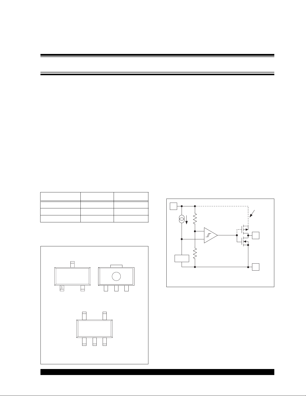
General Description
The TC54 Series are CMOS voltage detectors, suited
especially for battery-powered applications because of
their extremely low 1µA operating current and small
surface-mount packaging. Each part is laser trimmed to
the desired threshold voltage which can be specified
from 1.1V to 6.0V and 7.7V, for a 2% and 1.5V to 6.0V
for a 1% tolerance.
The device includes a comparator, low-current highprecision reference, laser-trimmed divider, hysteresis
circuit and output driver. The TC54 is available with
either an open-drain or complementary output stage.
In operation, the TC54's output (V
logic HIGH state as long as V
specified threshold voltage (V
below V
- the output is driven to a logic LOW. V
DET
remains LOW until VIN rises above V
amount V
, whereupon it resets to a logic HIGH.
HYST
) remains in the
OUT
is greater than the
IN
-). When VIN falls
DET
- by an
DET
OUT
Functional Block Diagram
2
V
IN
–
+
TC54VC only
V
OUT
1
3-Pin SOT-23A 3-Pin SOT-89
V
REF
T
132
V
OUT
5-Pin SOT-23A
NC
5
1
V
OUTVINVSS
NOTE: 3-Pin SOT-23A is equivalent to the EIAJ SC-59.
5-Pin SOT-23A is equivalent to the EIAJ SC-74A.
2002 Microchip Technology Inc. DS21434C-page 1
TC54
2
NC
4
3
TC54
V
V
IN
SS
TC54VN has open-drain output.
TC54VC has complementary output.
V
SS
3
Page 2
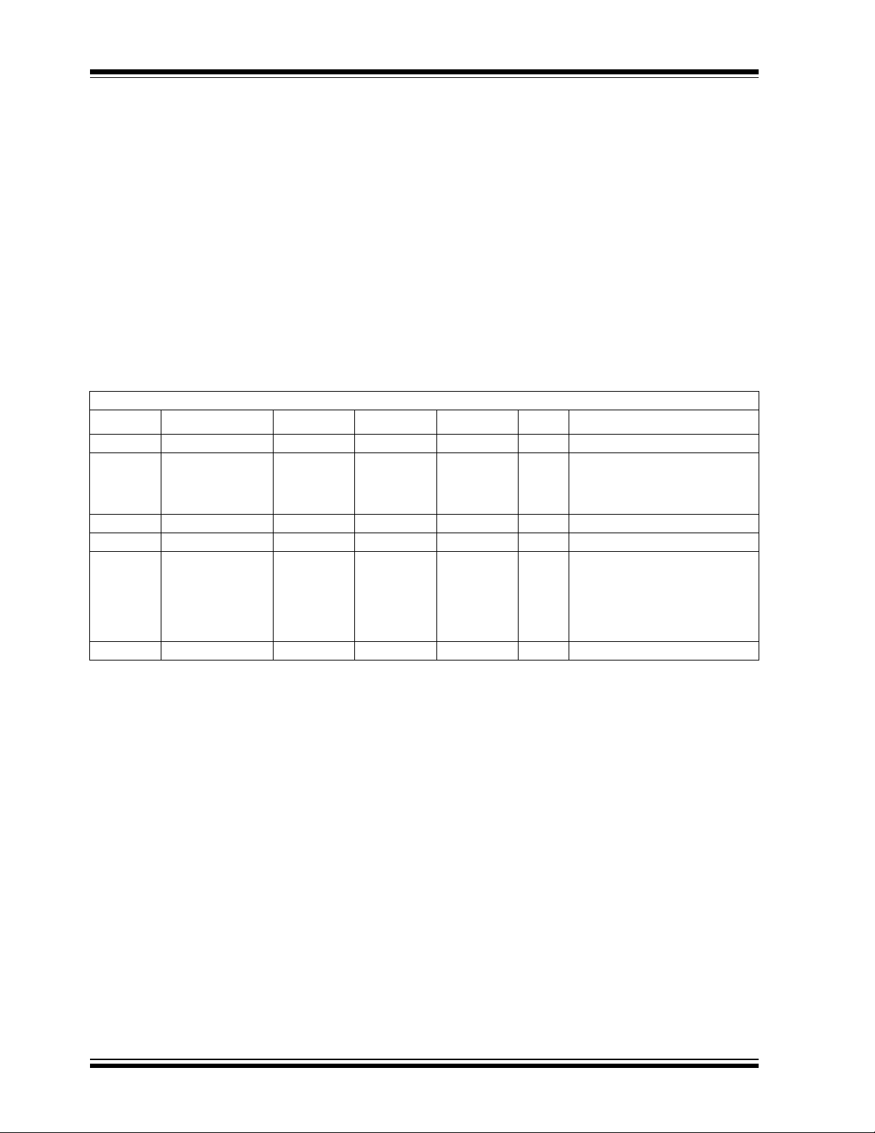
TC54
1.0 ELECTRICAL CHARACTERISTICS
Absolute Maximum Ratings*
Input Voltage ........................................................+12V
Output Current .................................................... 50mA
Output Voltage: CMOS..... (V
Open Drain ..........(V
Power Dissipation (T
≤ 70°C):
A
– 0.3V) to (VIN + 0.3V)
SS
– 0.3V) to 12V
SS
*Stresses above those listed under "Absolute Maximum
Ratings" may cause permanent damage to the device. These
are stress ratings only and functional operation of the device
at these or any other conditions above those indicated in the
operation sections of the specifications is not implied.
Exposure to Absolute Maximum Rating conditions for
extended periods may affect device reliability.
3-Pin SOT-23A...........................................240mW
3-Pin SOT-89 .............................................400mW
5-Pin SOT-23A...........................................240mW
Operating Temperature Range.............-40°C to +85°C
Storage Temperature Range..............-65°C to +150°C
TC54 ELECTRICAL SPECIFICATIONS
Electrical Characteristics: TA = 25°C, unless otherwise specified.
Symbol Parameter Min Typ Max Units Test Conditions
V
IN
I
SS
- Threshold Voltage V
V
DET
V
HYST
I
OUT
(V
T
C
DET
Operating Voltage 0.7 — 10.0 V (V
Quiescent Current —
Hysteresis Voltage V
Output Current —
-) Tempco of (V
1.0
—
—
—
- x 0.98 — V
DET
- x 0.02 V
DET
1.3
1.6
2.0
- x 0.05 V
DET
7.7
—
—
—
—
-) — ±100 — ppm/°C -40°C ≤ T
DET
10.1
11.5
13.0
-10.0
3.0
3.4
3.8
4.2
- x 1.02 V
DET
- x 0.08 V
DET
—
—
—
—
—
µAV
mA VOL = 0.5V, VIN = 2.1V
-) = 0.8 to 6.0V
DET
= 2.1V
IN
V
= 3.0V
IN
V
= 4.0V
IN
V
= 5.0V
IN
V
= 3.0V
IN
V
= 4.0V
IN
V
= 5.0V
≤ 85°C
A
IN
TC54VC Only;
V
= VIN – 2.1V, VIN = 8.0V
OH
DS21434C-page 2 2002 Microchip Technology Inc.
Page 3
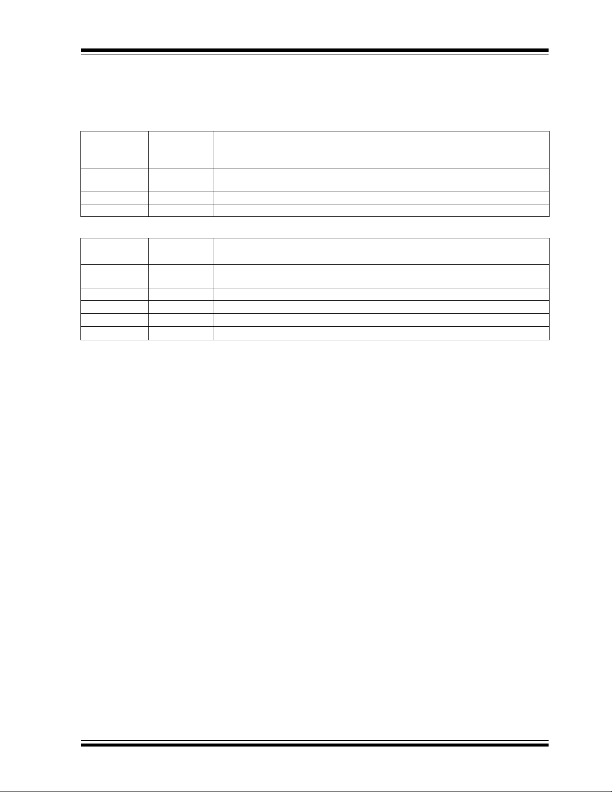
2.0 PIN DESCRIPTIONS
The descriptions of the pins are listed in Table 2-1.
TABLE 2-1: PIN FUNCTION TABLE
Pin No.
(3-Pin SOT-23A)
(3-Pin SOT-89)
1V
2V
3V
Symbol Description
OUT
IN
SS
Digital output. This output goes low when VIN drops below V
rises above V
Analog input. This pin is both the power supply input and the voltage to be monitored.
Ground terminal.
DET
- + V
. (See Figure 3-1, Timing Diagram.)
HYST
TC54
- and returns high when VIN
DET
Pin No.
(5-Pin SOT-23A)
1V
2V
3V
4 NC Not connected.
5 NC Not connected.
Symbol Description
OUT
IN
SS
Digital output. This output goes low when VIN drops below V
rises above V
Analog input. This pin is both the power supply input and the voltage to be monitored.
Ground terminal.
DET
- + V
. (See Figure 3-1, Timing Diagram.)
HYST
- and returns high when VIN
DET
2002 Microchip Technology Inc. DS21434C-page 3
Page 4
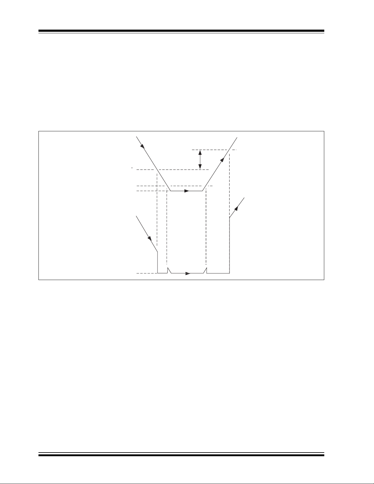
TC54
g
ge
ST
ge
ge
ge
OUT
3.0 DETAILED DESCRIPTION
In normal steady-state operation, when VIN > V
the output will be at a logic high, see Figure 3-1. In the
case of the TC54V, this is an open-drain condition. If
and when the input falls below V
pull down (Logic 0) to V
down to within 0.5V of V
. Generally, V
SS
at rated output current and
SS
-, the output will
DET
input voltage. (See Section 1.0, Electrical
Characteristics).
FIGURE 3-1: TIMING DIAGRAM
Detect Voltage V
Minimum Operatin
Volta
Ground Level
OUT
DET
can pull
The output, V
falls below the minimum operating voltage, V
-,
0.7V. Below this minimum operating voltage, the output
is undefined. During power-up or anytime V
below V
above V
valid. V
V
IN
< V
IN
IN
OUT
DET
the input rises above V
, will stay valid until the input voltage
OUT
has fallen
, V
will remain undefined until VIN rises
OUT
MIN
, at which time the output will become
MIN
IN
will be in its active low state while V
+. (V
DET
+ = V
- + V
DET
+, the output will assume its
DET
HYST
). If and when
, of
IN
MIN
<
IN
MIN
inactive state. (High for TC54VC, open-drain for
TC54VN).
Release Volta
HY
or RESET Volta
Output Volta
Ground Level
4.0 APPLICATIONS INFORMATION
Refer to Microchip Technology Application Note #779,
Using the TC54 Voltage Detector.
DS21434C-page 4 2002 Microchip Technology Inc.
Page 5

5.0 PACKAGING INFORMATION
5.1 Package Marking Information
TC54
3
1
represents output configuration (CMOS or Nch)
and first integer of voltage
Ex: CMOS 3.x =
D
Symbol Output Voltage
BCMOS1.
CCMOS2.
DCMOS3.
ECMOS4.
FCMOS5.
HCMOS6.
Symbol Output Voltage
LNch1.
MNch2.
NNch3.
PNch4.
RNch5.
SNch6.
TNch7.
represents first decimal of output voltage (0-9)
2
4
Ex: CMOS 3.x =
D
1
represents output configuration and first integer
of voltage
Symbol Output Voltage
TNch7.
2
represents first decimal of output voltage
Symbol Voltage
0.0
1.1
2.2
3.3
4.4
5.5
6.6
7.7
8.8
9.9
3
represents assembly lot code
4
&
3
2002 Microchip Technology Inc. DS21434C-page 5
represents assembly lot code
4
&
Page 6

TC54
5.2 Taping Form
Component Taping Orientation for 3-Pin SOT-23A (EIAJ SC-59) Devices
User Direction of Feed
Device
Marking
W
PIN 1
Standard Reel Component Orientation
for TR Suffix Device
(Mark Right Side Up)
Carrier Tape, Number of Components Per Reel and Reel Size
Package Carrier Width (W) Pitch (P) Part Per Full Reel Reel Size
3-Pin SOT-23A 8 mm 4 mm 3000 7 in
P
Component Taping Orientation for 3-Pin SOT-89 Devices
User Direction of Feed
Device
Marking
W
PIN 1
P
Standard Reel Component Orientation
for TR Suffix Device
(Mark Right Side Up)
Carrier Tape, Reel Size, and Number of Components Per Reel
Package Carrier Width (W) Pitch (P) Part Per Full Reel Reel Size
3-Pin SOT-89 12 mm 8 mm 1000 7 in
DS21434C-page 6 2002 Microchip Technology Inc.
Page 7

5.2 Taping Form (Continued)
Component Taping Orientation for 5-Pin SOT-23A (EIAJ SC-74A) Devices
Device
Marking
TC54
User Direction of Feed
W
PIN 1
Carrier Tape, Number of Components Per Reel and Reel Size
Package Carrier Width (W) Pitch (P) Part Per Full Reel Reel Size
5-Pin SOT-23A 8 mm 4 mm 3000 7 in
5.3 Package Dimensions
SOT-23A-3
.118 (3.00)
.098 (2.50)
PIN 1
P
Standard Reel Component Orientation
TR Suffix Device
(Mark Right Side Up)
.020 (0.50)
.012 (0.30)
.071 (1.80)
.055 (1.40)
.075 (1.90)
REF.
.122 (3.10)
.106 (2.70)
.051 (1.30)
.035 (0.90)
.006 (0.15)
.000 (0.00)
2002 Microchip Technology Inc. DS21434C-page 7
10° MAX.
.022 (0.55)
.014 (0.35)
Dimensions: inches (mm)
.010 (0.25)
.004 (0.09)
Page 8

TC54
5.3 Package Dimensions (Continued)
SOT-89-3
.181 (4.60)
.173 (4.39)
.071 (1.80)
.063 (1.60)
.063 (1.60)
.055 (1.40)
.019 (0.48)
.014 (0.36)
PIN 1
SOT-23A-5
.122 (3.10)
.098 (2.50)
.020 (0.50)
.012 (0.30)
.022 (0.56)
.016 (0.41)
PIN 1
.063 (1.60)
.055 (1.40)
.075 (1.90)
REF.
.019 (0.48)
.014 (0.36)
.037 (0.95)
.102 (2.59)
.090 (2.29)
.031 (0.79) MIN.
.071 (1.80)
.059 (1.50)
REF.
.167 (4.24)
.017 (0.43)
.014 (0.36)
Dimensions: inches (mm)
.122 (3.10)
.106 (2.70)
.057 (1.45)
.035 (0.90)
.006 (0.15)
.000 (0.00)
DS21434C-page 8 2002 Microchip Technology Inc.
10° MAX.
.024 (0.60)
.004 (0.10)
Dimensions: inches (mm)
.010 (0.25)
.004 (0.09)
Page 9

PRODUCT IDENTIFICATION SYSTEM
To order or obtain information, e.g., on pricing or delivery, refer to the factory or the listed sales office
PART CODE TC54V X XX X X X XX XXX
Output Configuration:
N = Nch Open Drain
C = CMOS Output
Detected Voltage:
Ex: 15 = 1.5V; 60 = 6.0V
Ex: 11 = 1.1V; 60 = 6.0V
Extra Feature Code:
Fixed: 0
Tolerance:
1 = ±1% (custom)
2 = ±2% (standard)
Temperature:
E: -40°C to +85°C
Package Type and Pin Count:
CB: 3-Pin SOT-23A (equivalent to EIAJ SC-59)
MB: 3-Pin SOT-89
CT: 5-Pin SOT-23A (equivalent to EIAJ SC-74A)
TC54
Taping Direction:
TR: Standard Taping
Sales and Support
Data Sheets
Products supported by a preliminary Data Sheet may have an errata sheet describing minor operational differences and recommended workarounds. To determine if an errata sheet exists for a particular device, please contact one of the following:
1. Your local Microchip sales office
2. The Microchip Corporate Literature Center U.S. FAX: (480) 792-7277
3. The Microchip Worldwide Site (www.microchip.com)
Please specify which device, revision of silicon and Data Sheet (include Literature #) you are using.
New Customer Notification System
Register on our web site (www.microchip.com/cn) to receive the most current information on our products.
2002 Microchip Technology Inc. DS21434C-page9
Page 10

TC54
NOTES:
DS21434C-page10 2002 Microchip Technology Inc.
Page 11

TC54
Information contained in this publication regarding device
applications and the like is intended through suggestion only
and may be superseded by updates. It is your responsibility to
ensure that your application meets with your specifications.
No representation or warranty is given and no liability is
assumed by Micr ochip Technology Incorporated with respect
to the accuracy or use of such information, or infringement of
patents or other intellectual property rights arising from such
use or otherwise. Use of Microchip’s products as critical components in life support systems is not authorized except with
express written approval by Microchip. No licenses are conveyed, implicitly or otherwise, under any intellectual property
rights.
Trademarks
The Microchip name and logo, the Microchip logo, FilterLab,
K
EELOQ
, microID, MPLAB, MXDEV, PIC, PICmicro,
PICMASTER, PICSTART, PRO MATE, SEEVAL and The
Embedded Control Solutions Company are registered trademarks of Microchip Technology Incorporated in the U.S.A. and
other countries.
dsPIC, dsPICDEM.net, ECONOMONITOR, FanSense,
FlexROM, fuzzyLAB, In-Circuit Serial Programming, ICSP,
ICEPIC, microPort, Migratable Memory, MPASM, MPLIB,
MPLINK, MPSIM, MXLAB, PICC, PICDEM, PICDEM.net,
rfPIC, Select Mode and Total Endurance are trademarks of
Microchip Technology Incorporated in the U.S.A.
Serialized Quick Turn Programming (SQTP) is a service mark
of Microchip Technology Incorporated in the U.S.A.
All other trademarks mentioned herein are property of their
respective companies.
© 2002, Microchip Technology Incorporated, Printed in the
U.S.A., All Rights Reserved.
Printed on recycled paper.
2002 Microchip Technology Inc. DS21434C-page 11
Page 12

M
W
ORLDWIDE SALES AND SERVICE
AMERICAS
Corporate Office
2355 West Chandler B lvd.
Chandler, AZ 85224-6199
Tel: 480-792-7200 Fax: 480-792-7277
Technical Support: 480-792-7627
Web Address: http://www.microchip.com
Rocky Mountain
2355 West Chandler B lvd.
Chandler, AZ 85224-6199
Tel: 480-792-7966 Fax: 480-792-4338
Atlanta
500 Sugar Mill Road, Suite 200B
Atlanta, GA 30350
Tel: 770-640-0034 Fax: 770-640-0307
Boston
2 Lan Drive, Suit e 120
Westford, MA 01886
Tel: 978-692-3848 Fax: 978-692-3821
Chicago
333 Pierce Road, S uite 180
Itasca, IL 60143
Tel: 630-285-0071 Fax: 630-285-0075
Dallas
4570 Westgrove Drive, Suite 160
Addison, TX 75001
Tel: 972-818-7423 Fax: 972-818-2924
Detroit
Tri-Atria Office Building
32255 Northwestern Highway, Suite 190
Farmington Hills, MI 48334
Tel: 248-538-2250 Fax: 248-538-2260
Kokomo
2767 S. Albright Road
Kokomo, Indiana 46902
Tel: 765-864-8360 Fax: 765-864-8387
Los Angeles
18201 Von Karman, Suite 10 90
Irvine, CA 92612
Tel: 949-263-1888 Fax: 949-263-1338
New York
150 Motor Parkwa y, Suite 202
Hauppauge, NY 11788
Tel: 631-273-5305 Fax: 631-273-5335
San Jose
Microchip Technology Inc.
2107 North First S treet, Suite 590
San Jose, CA 95131
Tel: 408-436-7950 Fax: 408-436-7955
Toro nto
6285 Northam Drive, Suite 108
Mississauga, Ontario L4V 1X5, Canada
Tel: 905-673-0699 Fax: 905-673-6509
ASIA/PACIFIC
Australia
Microchip Technology Australia Pty Ltd
Suite 22, 41 Rawson Street
Epping 2121, NSW
Australia
Tel: 61-2-9868-6733 Fax: 61-2-9868-6755
China - Beijing
Microchip Technology Consulting (Shanghai)
Co., Ltd., Beijing Liaison Office
Unit 915
Bei Hai Wan Tai Bldg.
No. 6 Chaoyangmen Beidajie
Beijing, 100027, No. China
Tel: 86-10-852821 00 Fax: 86-10-85282104
China - Chengdu
Microchip Technology Consulting (Shanghai)
Co., Ltd., Chengdu Liaison Office
Rm. 2401, 24th Floor,
Ming Xing Financial Tower
No. 88 TIDU Street
Chengdu 610016, China
Tel: 86-28-867662 00 Fax: 86-28-86766599
China - Fuzhou
Microchip Technology Consulting (Shanghai)
Co., Ltd., Fuzhou Liaison Office
Unit 28F, World Trade Plaza
No. 71 Wusi Road
Fuzhou 350001, China
Tel: 86-591-75035 06 Fax: 86-591-7503521
China - Shanghai
Microchip Technology Consulting (Shanghai)
Co., Ltd.
Room 701, Bldg. B
Far East International Plaza
No. 317 Xian Xia Road
Shanghai, 200051
Tel: 86-21-6275-5700 Fax: 86-21-6275 -5060
China - Shenzhen
Microchip Technology Consulting (Shanghai)
Co., Ltd., Shenzhen L iaison Office
Rm. 1315, 13/F, Shenzhen Kerry Centre,
Renminnan Lu
Shenzhen 518001, Ch ina
Tel: 86-755-23503 61 Fax: 86-755-2366086
China - Hong Kong SAR
Microchip Technology Hongkong Ltd.
Unit 901-6, Tower 2, Metroplaza
223 Hing Fong Road
Kwai Fong, N.T., Hong Kong
Tel: 852-2401-120 0 Fax: 852-2401-3431
India
Microchip Technology Inc.
India Liaison Office
Divyasree Chambers
1 Floor, Wing A (A3/A4)
No. 11, O’Shaugnessey Road
Bangalore, 560 025, India
Tel: 91-80-229006 1 Fax: 91-80-2290062
Japan
Microchip Technology Japan K.K.
Benex S-1 6F
3-18-20, Shinyokohama
Kohoku-Ku, Yokohama-shi
Kanagawa, 222-0033, Japan
Tel: 81-45-471- 6166 Fax: 81-45-471-6122
Korea
Microchip Technology Korea
168-1, Youngbo Bldg. 3 Floor
Samsung-Dong, Kangnam-Ku
Seoul, Korea 135-882
Tel: 82-2-554-7200 Fax: 82-2-558-5934
Singapore
Microchip Technology Singapore Pte Ltd.
200 Middle Road
#07-02 Prime Centre
Singapore, 188980
Tel: 65-6334-8870 Fax: 65-6334-8850
Ta iw an
Microchip Technology (Barbados) Inc.,
Taiwan Branch
11F-3, No. 207
Tung Hua North Road
Taipei, 105, Taiwan
Tel: 886-2-2717-7175 Fax: 886-2-2545-0139
EUROPE
Denmark
Microchip Technology Nordic ApS
Regus Business Centre
Lautrup hoj 1-3
Ballerup DK-2750 Denmark
Tel: 45 4420 9895 Fax: 45 4420 9910
France
Microchip Technology SARL
Parc d’Activite du Moulin de Massy
43 Rue du Saule Trapu
Batiment A - ler Etage
91300 Massy, France
Tel: 33-1-69-53-63-20 Fax: 33-1-69-30-90-79
Germany
Microchip Technology GmbH
Gustav-Heinemann Ring 125
D-81739 Munich, Germany
Tel: 49-89-627-144 0 Fax: 49-89-627-144-44
Italy
Microchip Technology SRL
Centro Direzionale Colleoni
Palazzo Taurus 1 V. Le Colleoni 1
20041 Agrate Brianza
Milan, Italy
Tel: 39-039-65791-1 Fax: 39-039-689988 3
United Kingdom
Microchip Ltd.
505 Eskdale Road
Winnersh Triangle
Wokingham
Berkshire, England RG41 5TU
Tel: 44 118 921 5869 Fax: 44-118 921-5820
Austria
Microchip Technology Austria GmbH
Durisolstrasse 2
A-4600 Wels
Austria
Tel: 43-7242-2244-399
Fax: 43-7242-2244-393
05/16/02
DS21434C-page 12 2002 Microchip Technology Inc.
 Loading...